

Yamaha RXA-730 Service Manual
RX-V675/HTR-6066/RX-A730/TSR-6750
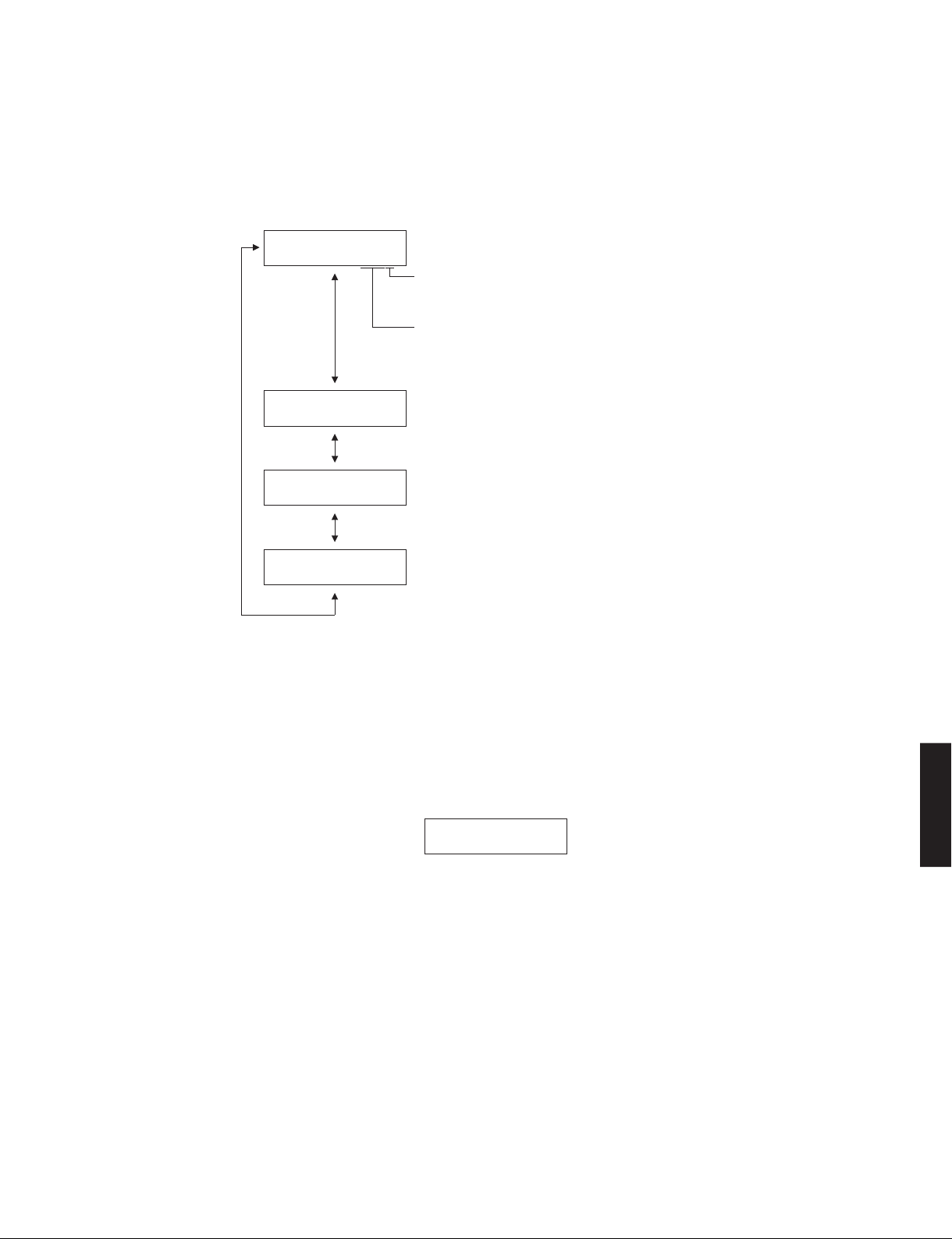
T3. EXTERNAL EVENT
This menu is used to display the history of key operation.
* No matter how many times the same key is pressed, it will be stored only once as its history.
* The key operation during the self-diagnostic function mode will not be stored.
All history of key operation will be erased by pressing the “STRAIGHT” key.
* Numeric values in the figure are given as reference only.
T3-1. HISTORY 1
T3-1
7E-2A
T3-5. HISTORY 5
T3-5
7A-DE
T3-2. HISTORY 2
T3-2
7A-AA
T3-6. HISTORY 6
T3-6
7A-9E
T3-3. HISTORY 3
T3-3
7A-9C
T3-7. HISTORY 7
T3-7
7A-9C
T3-4. HISTORY 4
T3-4
7A-AA
T3-8. HISTORY 8
T3-8
7A-AA
RX-A730/TSR-6750
61
RX-V675/HTR-6066/
RX-V675/HTR-6066/RX-A730/TSR-6750
List of key operation
Display
Key number AD value 1 AD value 2 AD value 3
Key name
0205 77 – 89 FF FF MAIN ZONE
0208 40 – 53 FF FF ZONE 2
020F 77 – 89 00 – 09 FF MAIN ZONE
+ STRAIGHT (Advanced setup mode)
0211 xx FF FF HD Radio CDM mode (U model)
0212 xx FF FF HD Radio SPLIT mode (U model)
0300 2D – 3F FF FF SCENE 1 (BD/DVD)
0301 1C – 2C FF FF SCENE 2 (TV)
0302 0A – 1B FF FF SCENE 3 (NET)
0303 00 – 09 FF FF SCENE 4 (RADIO)
0500 FF 9C – AD FF PROGRAM
0501 FF 8A – 9B FF PROGRAM
0526 FF 0 – 9 FF STRAIGHT
0529 FF FF 9C – AD PURE DIRECT
0800 FF 0A – 1B FF TONE CONTROL
0A00 FF FF 2D – 3F INFO
0C00 FF FF D2 – E3 ZONE CONTROL
2C00 FF FF 8A – 9B TUNING
2C01 FF FF 77 – 89 TUNING
2C02 FF FF 65 – 76 AM
2C03 FF FF 54 – 64 FM
2C04 FF FF 00 – 09 PRESET
2C05 FF FF 0A – 1B PRESET
2C06 FF FF 40 – 53 MEMORY
0101 VOLUME knob (–)
0102 VOLUME knob (+)
0103 INPUT knob (–) (RX-A730)
0104 INPUT knob (+) (RX-A730)
7A xxxx * For the details of the remote control key display, refer to
7E xxxx “REMOTE CONTROL”.
RX-A730/TSR-6750
RX-V675/HTR-6066/
62
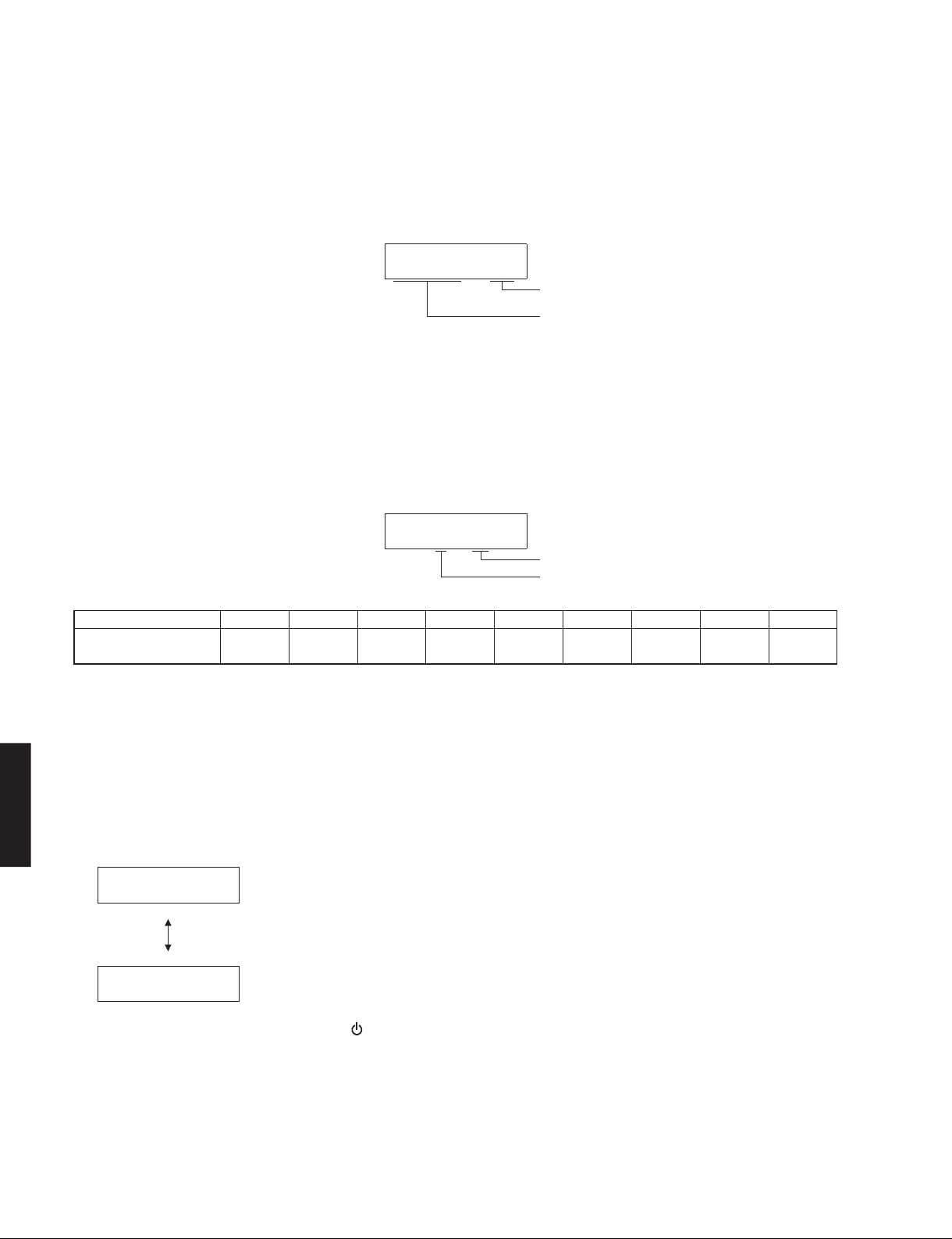
T4. INTERNAL INFORMATION
T4-1. DSP INFORMATION
This menu is used to display the DSP information stored in memory as backup data before rebooting.
The DSP information will be erased by pressing the ‘STRAIGHT “ key.
Display Sampling frequency [kHz]
032
1 44.1
248
364
4 88.2
596
6128
7 176.4
8192
10 8
11 11
12 12
13 16
14 22.05
15 24
16 “Unknown”
T4-1
DSP:--/--/--
Display Channels
0 Dual Mono
1 1/0
2 2/0
3 3/0
4 2/1
5 3/1
6 2/2
7 3/2
8 2/3
9 3/3
10 2/4
11 3/4
12 HD Multi channel
13 “Unknown”
RX-V675/HTR-6066/RX-A730/TSR-6750
--: Not stored
Decode format
Channels
Sampling frequency
Decode formatChannelsSampling frequency
Display Decode format
0 Analog
1 PCM
2 Dolby Digital
3 Dolby Digital EX
4 DTS
5 DTS 9624
6 DTS ES Matrix
7 DTS ES Discrete
8 DTS 96 ES Matrix
9AAC
10 DSD
11 Multi PCM
12 Dolby Digital Plus
13 Dolby Digital Plus EX
14 Dolby True HD
15 Dolby True HD EX
16 DTS Express
17 DTS HD
18 DTS HD Master Audio
19 Digital
20 MP3
21 WMA
22 FLAC
25 “Unknown”
RX-V675/HTR-6066/
RX-A730/TSR-6750
T4-2. BU ERROR
Not for service.
T4-3. NRC (Net Restart Counter)
Not for service.
T4-4. INVALID ITEM
Not for service.
T4-2
BUERR:-255
T4-3
NRC:0
T4-4
INVALIDITEM
63

RX-V675/HTR-6066/RX-A730/TSR-6750
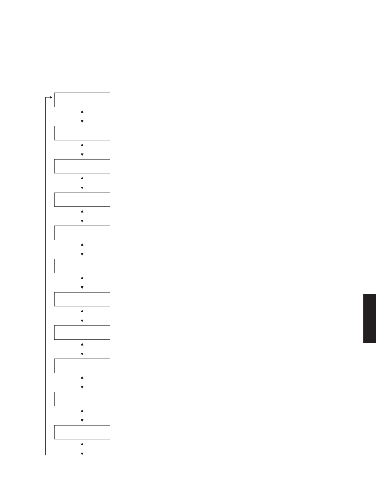
P1. SYSTEM MONITOR
This menu is used to display the A/D conversion value of the microprocessor which detects panel keys and protection
functions by using the sub-menu.
When “P1-8. KEY” sub-menu is selected, keys become inoperable due to detection of the values of all keys.
However, it is possible to advance to the next menu by pressing the “SCENE RADIO” (forward) key or “SCENE NET”
(reverse) key on the remote control.
* Numeric values in the figure are given as reference only.
P1-1. DC
Power amplifier DC (DC voltage) output is detected.
The voltage at 5 pin (DC_PRT) of IC78 is displayed.
Normal value: 32 to 74
(Reference voltage: 3.3 V=255)
* If DC becomes out of the normal value range, the protection function works to turn off the power.
P1-1
DC:50
RX-A730/TSR-6750
RX-V675/HTR-6066/
P1-2. PS
Power supply voltage (PS) protection detection.
The voltage at 2 pin (PS1_PRT)/1 pin (PS2_PRT)/13 pin (PS3_PRT) of IC78 are displayed.
Voltage detects
PS1: ACBL, AC12, AC5, ±7
PS2: -VP, +5T, ±5V
PS3: +5.5V
Normal value
PS1: 51 to 179
PS2: 92 to 147 (PURE DIRECT mode: 139 to 193)
PS3: 132 to 168
(Reference voltage: 3.3 V=255)
* If PS1, PS2 or PS3 becomes out of the normal value range, the protection function works to turn off the
power.
P1-2
PS:117/120/153
PS3
PS2
PS1
64

RX-V675/HTR-6066/RX-A730/TSR-6750
P1-3. THM
Temperature of the heatsink (THM) is detected.
The voltage at 12 pin (THM1) of IC78/1 pin (THM2) of IC76 are displayed.
Normal value
THM1: 42 to 255
THM2: 42 to 255 (U, C models)
(Reference voltage: 3.3 V=255)
* If THM1 or THM2 becomes out of the normal value range, the protection function works to turn off the power.
P1-3
TMa:112/105
THM2
THM1
P1-4. INVALID ITEM
Not for service.
P1-5. OUTPUT LEVEL
Output level of speaker output is detected.
The voltage at 4 pin (AMP_OLV) of IC78 is displayed.
(Reference voltage: 3.3 V=255)
P1-6. LIMITER CONTROL
Power limiter control is detected.
The voltage at 4 pin (AMP_LMT) of IC83 is displayed.
(Reference voltage: 3.3 V=255)
P1-4
INVALIDITEM
P1-5
OUTLVL:255
P1-6
LMTCNT:255
RX-V675/HTR-6066/
RX-A730/TSR-6750
P1-7. L3 (J model)
Not for service.
P1-7
L3:0
65
RX-V675/HTR-6066/RX-A730/TSR-6750
P1-8. KEY
Panel key is detected.
When the A/D conversion value of the panel key becomes out of the specified range, normal operation will not
be available.
In that case, check the constant of voltage dividing resistor, solder condition, etc. Refer to table.
* When “P1-8. KEY” menu is selected, keys become inoperable due to detection of the values of all keys.
However, it is possible to advance to the next menu by pressing the “SCENE RADIO” (forward) key or “SCENE
NET” (reverse) key on the remote control.
(Reference voltage: 3.3 V=255)
P1-8
KY:255/255
KEY2
KEY1
RX-A730/TSR-6750
RX-V675/HTR-6066/
Display KEY1
0 – 11
12 – 32
33 – 54
55 – 75
76 – 96
97 – 119 ZONE2
120 – 142
143 – 172
173 – 202
203 – 235
255 Key off
(RX-V675/HTR-6066/TSR-6750 models)
(RX-V675/HTR-6066/TSR-6750 models)
RADIO
(SCENE4)
NET
(SCENE3)
TV
(SCENE2)
BD/DVD
(SCENE1)
ZONE
CONTROL
INPUT >
INPUT <
MAIN ZONE
TONE
CONTROL
Display KEY2
0 – 11
12 – 32
33 – 54
55 – 77 AM
78 – 99 FM
100 – 121
122 – 144
145 – 166 MEMORY
167 – 186 INFO
187 – 205 STRAIGHT
206 – 226
227 – 246
255 Key off
PURE
DIRECT
TUNING
>>
TUNING
<<
PRESET
>
PRESET
<
PROGRAM
>
PROGRAM
<
66
P1-9. USB-VBUS
Not for service.
P1-9
USB-VBUS:3
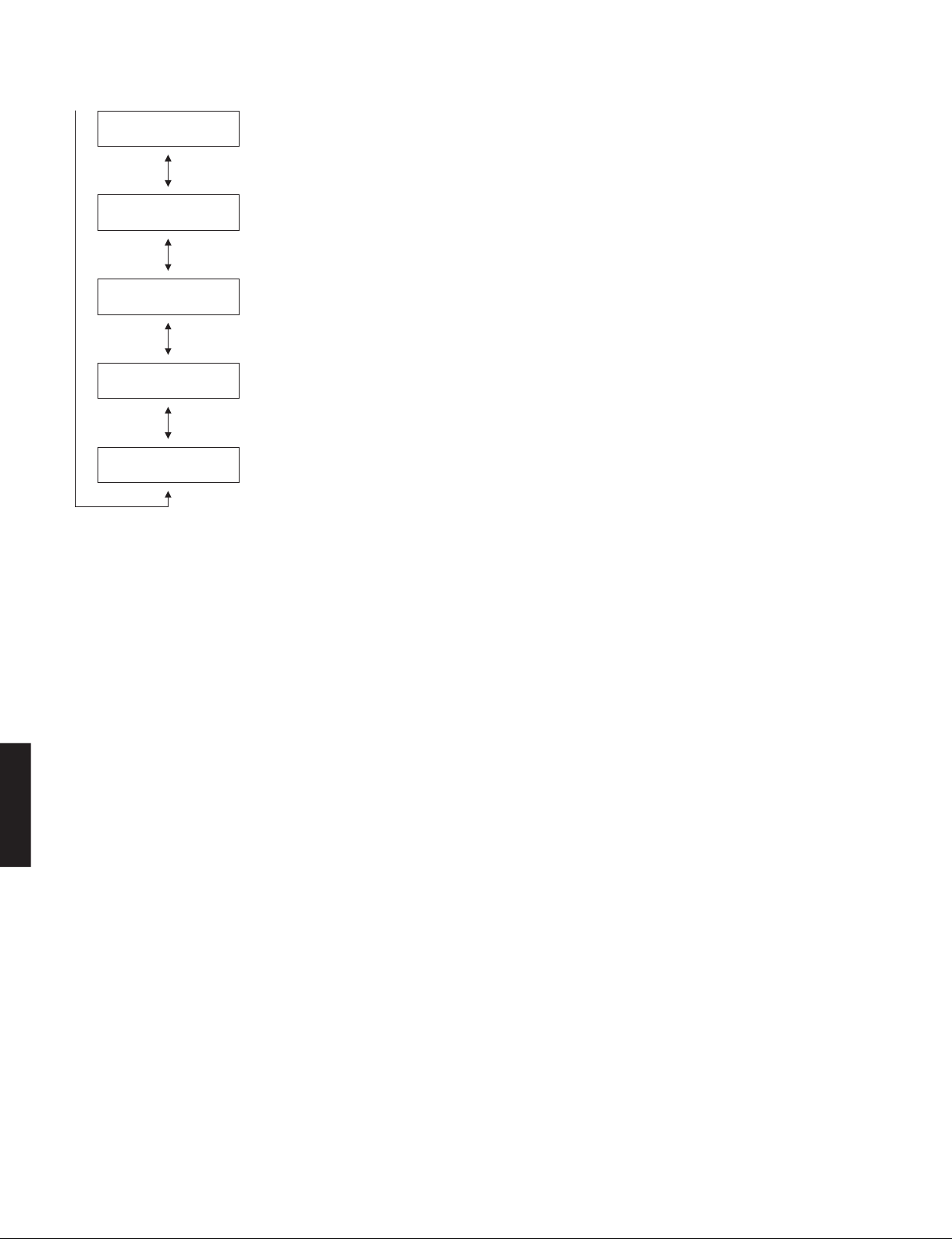
P2. PROTECTION HISTORY
This menu is used to display the history of protection function.
All history of protection function will be erased by pressing the “STRAIGHT” key.
* Numeric values in the figure are given as reference only.
RX-V675/HTR-6066/RX-A730/TSR-6750
P2-1
1st:PS2000L
P2-2
2nd:TMP1000L
P2-3
3rd:DC000L
P2-4
NoPrt
P2-1. History 1
H: Displayed when the voltage is HIGHER than upper limit.
L: Displayed when the voltage is LOWER than lower limit.
xxx: A/D conversion value of voltage at the moment when the protection function
worked.
(Reference voltage: 3.3 V=255)
P2-2. History 2
P2-3. History 3
P2-4. History 4
S1. FIRMWARE UPDATE
Not for service.
S1-1
F/WUPDATE?
RX-A730/TSR-6750
67
RX-V675/HTR-6066/
RX-V675/HTR-6066/RX-A730/TSR-6750
S2. SET INFORMATION
The model name and destination of this unit are displayed.
S2-1. MODEL
The model name of this unit is displayed.
S2-2. DESTINATION
The destination of this unit is displayed.
S2-1
MDL:V675255
Not for service.
Model name
V675 : RX-V675
6066 : HTR-6066
A730 : RX-A730
6750 : TSR-6750
S3. FACTORY PRESET
RX-A730/TSR-6750
RX-V675/HTR-6066/
S2-2
DEST:U28
A/D conversion value
Destination
Destination J U C R (R, S) T K A BG (B, G, F) L (L, H)
A/D conversion value
(3.3 V=255)
0 − 12 13 − 39 40 − 67 68 − 92 93 − 115 116 − 140 141 − 169 199 − 221 222 − 244
This menu is used to reserve/inhibit initialization of the back-up IC (EEPROM: IC82 on DIGITAL P.C.B.).
S3-1
PRESET:INH
S3-1
PRESET:RSRV
S3-1. PRESET INHIBIT (Initialization inhibited)
Initialization of the back-up IC is not executed. Select this sub-menu to protect the values set by the user.
S3-1. PRESET RESERVED (Initialization reserved)
Initialization of the back-up IC is reserved. (Actual initialization is executed when the power is turned on
next.) To reset to the original factory settings or to reset the backup IC, select this sub-menu and press
the “MAIN ZONE
” key to turn off the power.
68
CAUTION: Before setting to the PRESET RESERVED, write down the existing preset memory content of the tuner. (This
is because setting to the PRESET RESERVED will cause the user memory content to be erased.)
RX-V675/HTR-6066/RX-A730/TSR-6750
S4. ROM VERSION/CHECKSUM
The firmware version and checksum values are displayed.
The checksum is obtained by adding the data at every 8-bit and expressing the result as a hexadecimal notation.
* Numeric values in the figure are given as reference only.
S4-1
SYS-VER.1.01
S4-2
VER.00028
S4-3
SUM.36F8
S4-4
FR-V.00029
S4-5
FR-S.1B05
S4-6
S-VER.0028
S4-1. SYSTEM VERSION
The firmware version is displayed.
S4-2. MICROPROCESSOR VERSION
The firmware version of MICROPROCESSOR (IC83 on DIGITAL (1) P.C.B.) is displayed.
S4-3. MICROPROCESSOR CHECKSUM
The checksum value of MICROPROCESSOR (IC83 on DIGITAL (1) P.C.B.) is displayed.
S4-4. FLASH ROM VERSION
The firmware version of FLASH ROM (IC77 on DIGITAL (1) P.C.B.) is displayed.
S4-5. FLASH ROM CHECKSUM
The checksum value of FLASH ROM (IC77 on DIGITAL (1) P.C.B.) is displayed.
S4-6. NETWORK MICROPROCESSOR VERSION
The firmware version of Network microprocessor (IC951 on DIGITAL (1) P.C.B.) is displayed.
S4-7
S-SUM.E47680D8
S4-8
D1-V.1.08r2
S4-9
D1-S.FC6FA124
S4-10
INVALIDITEM
S4-11
INVALIDITEM
S4-7. NETWORK MICROPROCESSOR CHECKSUM
The checksum value of Network microprocessor (IC951 on DIGITAL (1) P.C.B.) is displayed.
S4-8. DSP1 VERSION
The firmware version of DSP1 (IC921 on DIGITAL (1) P.C.B.) is displayed.
S4-9. DSP1 CHECKSUM
The checksum value of DSP1 (IC921 on DIGITAL (1) P.C.B.) is displayed.
S4-10. INVALID ITEM
Not for service.
S4-11. INVALID ITEM
Not for service.
RX-V675/HTR-6066/
RX-A730/TSR-6750
69
RX-V675/HTR-6066/RX-A730/TSR-6750
S4-12
G-V.000000228
S4-13
FPGA-G-V.25
S4-14
FPGA-S-V.24
S4-15
FPGA-H-V.11
S4-16
INVALIDITEM
S4-12. GUI VERSION
The firmware version of GUI data is displayed.
S4-13. FPGA GUI VERSION
The firmware version of GUI section in FPGA (IC50 on DIGITAL (1) P.C.B.) is displayed.
S4-14. FPGA SD (Standard Definition) VERSION
The firmware version of SD I/P scaler section in FPGA (IC50 on DIGITAL (1) P.C.B.) is displayed.
S4-15. FPGA HD (High Definition) VERSION
The firmware version of HD I/P scaler section in FPGA (IC50 on DIGITAL (1) P.C.B.) is displayed.
S4-16. INVALID ITEM
Not for service.
RX-A730/TSR-6750
RX-V675/HTR-6066/
70
RX-V675/HTR-6066/RX-A730/TSR-6750
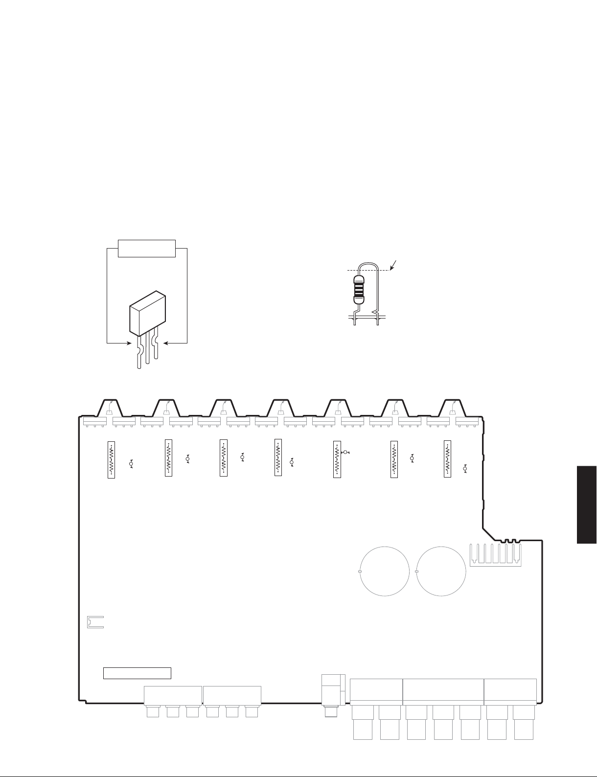
■ POWER AMPLIFIER ADJUSTMENT
1. Right after power is turned on, confirm that the voltage across the terminals of R1152 (SURROUND BACK Rch), R1154
(SURROUND Rch), R1150 (FRONT Rch), R1148 (CENTER), R1149 (FRONT Lch), R1153 (SURROUND Lch) and R1151
(SURROUND BACK Lch) are within the confines of 0.1 mV to 10 mV.
2. If measured voltage exceeds 10 mV, open (cut off) R1104 (SURROUND BACK Rch), R1106 (SURROUND Rch), R1102 (FRONT
Rch), R1100 (CENTER), R1101 (FRONT Lch), R1105 (SURROUND Lch) and R1103 (SURROUND BACK Lch), and then
reconfirm the voltage.
Attention
If the measured voltage exceeds 10 mV after repairing the power amplifier, check other parts again for any possible
defect before cutting the resistor.
3. Confirm that the voltage is within the confines of 0.2 mV to 15 mV after 60 minutes.
0.1 mV – 10 mV
(DC)
R1152 (SURROUND BACK Rch)
R1154 (SURROUND Rch)
R1150 (FRONT Rch)
R1148 (CENTER)
R1149 (FRONT Lch)
R1153 (SURROUND Lch)
R1151 (SURROUND BACK Lch)
Open (cut off)
R1104 (SURROUND BACK Rch)
R1106 (SURROUND Rch)
R1102 (FRONT Rch)
R1100 (CENTER)
R1101 (FRONT Lch)
R1105 (SURROUND Lch)
R1103 (SURROUND BACK Lch)
R1154
R1106
MAIN (1) P.C.B.
R1153 R1152
R1105
R1104
R1151
Front side
R1103
R1150
R1102
R1149
R1101
R1148
R1100
RX-V675/HTR-6066/
RX-A730/TSR-6750
71
RX-V675/HTR-6066/RX-A730/TSR-6750
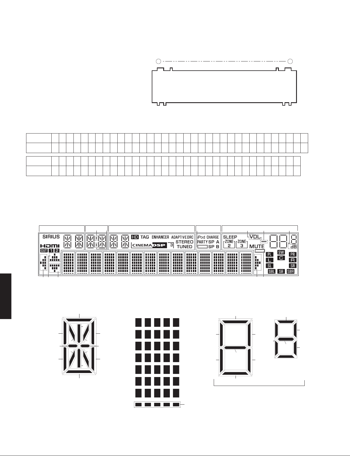
■ DISPLAY DATA
● V3001 : 18-MT-11GNAK (OPERATION P.C.B.)
69
PATTERN AREA
● PIN CONNECTION
Pin No.
Connection
Pin No.
Connection
Note : 1) F1, F2 ..... Filament pin 2) NP ..... No pin 3) NX ..... No extend pin 4) 1G-18G ..... Grid pin
● GRID ASSIGNMENT
69
68 67NP66NP65P164P263P362P461P560P659P758P857P956
F2NX
34
P3233P3332P3431P3530P36
18G
1a 1a1a2a 2a2a 2a1a
29 28
NXNX27NX26NX25NX24NX23NX2218G2117G2016G1915G1814G1713G1612G1511 G1410G139G128G117G106G95G84G73G62G51G4NP3NP
17G
S8 S9
P1055P1154P1253P1352P1451P1550P1649P1748P1847P1946P2045P2144P2243P2342P2441P2540P2639P2738P2837P29
16G
17G
1
36
P3035P31
21
F1NX
15G
S7 S5S15 S5
RX-A730/TSR-6750
RX-V675/HTR-6066/
72
S12
S11
S10
f
gm
e
2G1G 3G 4G 5G 6G 7G 11G10G9G8G 12G 13G 14G
a
j
b
h
k
nr
c
p
d
(18G–16G)
1-1 2-1 3-1 4-1 5-1
1- 2
2-2
3-2
1- 3
2-3
3-3
1- 4
2-4
3-4
1- 5
2-5
3-5
1- 6
2-6
3-6
1- 7
2-7
3-7
4-2
4-3
4-4
4-5
4-6
4-7
5-2
5-3
5-4
5-5
5-6
5-7
(1G–14G)
S1
S13
S6
a
f
g
e
d
b
c
S2
S3
S3
S4
S2
(15G)
RX-V675/HTR-6066/RX-A730/TSR-6750
● ANODE CONNECTION
18G 17G 16G 15G 1G-14G
P1 1a 1a 1a S5 1-1
P2 1h 1h 1h S7 2-1
P3 1j 1j 1j 1d 3-1
P4 1k 1k 1k 2d 4-1
P5 1b 1b 1b S2 5-1
P6 1f 1f 1f 1e 1-2
P7 1m 1m 1m 2e 2-2
P8 1g 1g 1g S3 3-2
P9 1c 1c 1c 1c 4-2
P10 1e 1e 1e 2c 5-2
P11 1r 1r 1r S4 1-3
P121p1p1p1g2-3
P131n1n1n2g3-3
P14 1d 1d 1d 1f 4-3
P15 2a 2a 2a 2f 5-3
P162h2h2h1b1-4
P17 2j 2j 2j 2b 2-4
P18 2k 2k 2k 1a 3-4
P192b2b2b2a4-4
P20 2f 2f 2f
P21 2m 2m 2m 1- 5
P22 2g 2g 2g 2-5
P23 2c 2c 2c 3-5
P24 2e 2e 2e
P25 2r 2r 2r 5-5
P26 2p 2p 2p 1- 6
P27 2n 2n 2n 2-6
P28 2d 2d 2d
P29
P30 S9 5-6
S8 4-6
5-4
4-5
3-6
RX-V675/HTR-6066/
RX-A730/TSR-6750
P31 S6 1-7
P32
P33 S15 3-7
P34 S12 4-7
P35 S10 5-7
P36 S11 – S1
S13 2-7
73
RX-V675/HTR-6066/RX-A730/TSR-6750
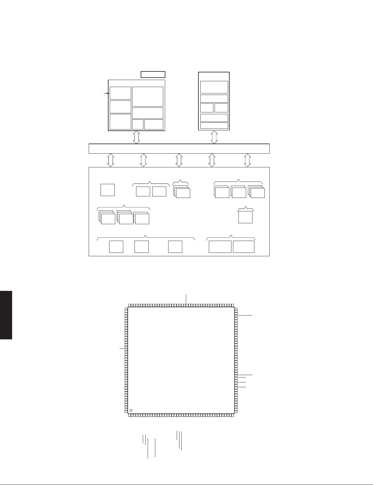
■ IC DATA
IC921: D80YK113CPTP400 (DIGITAL (1) P.C.B.)
DSP (Digital signal processor)
Input
Clock(s)
Peripherals
System Control
(Watchdog)
GPIO
eHRPWM
USB2.0
OTG Ctlr
PLL/Clock
Generator
w/OSC
GeneralPurpose
Timer
GeneralPurpose
Timer
Control Timers
eCAP
PHY
JTAG Interface
Memory Protection
I/O Protection
Power/Sleep
Controller
RTC/
OSC
Pin
Multiplexing
32-KHz
Switched Control Resource (SCR)
DMA
EDMA3
eQEP
Connectivity
HPI
dMAX
Audio Ports
MMC/SD
(8b)
McASP
w/FIFO
DSP Subsystem
TM
C674x
DSP MICRO-
PROCESSOR
AET
32 KB
32 KB
L1 Pgm
L1 RAM
256 KB L2 RAM
1024 KB L2 ROM
I2C SPI
External Memory Interface
EMIFA(8b/16b)
NAND/Flash
16b SDRAM
Serial Interface
Shared Memory
128 KB
RAM
EMIFB
SDRAM Only
(16b/32b)
UART
RX-A730/TSR-6750
RX-V675/HTR-6066/
74
USB0_VDDA12
USB0_VDDA18
USB0_DP
USB0_DM
USB0_VDDA33
PLL0_VDDA
PLL0_VSSA
OSCIN
OSCVSS
OSCOUT
RESET
RTC_XI
RTC_CVDD
GP7[14]
AHCLKX1/EPWMQB/GP3[14]
ACLKX1/EPWMQA/GP3[15]
AFSX1/EPWMSYNCI/EPWMSYNC0/GP4[10]
ACLKR1/ECAP2/APWM2/GP4[12]
AFSR1/GP4[13]
AXR1[8]/EPWM1A/GP4[8]
AXR1[7]/EPWM1B/GP4[7]
AXR1[6]/EPWM2A/GP4[6]
AXR1[5]/EPWM2B/GP4[5]
AXR1[4]/EQEP1B/GP4[4]
AXR1[3]/EQEP1A/GP4[3]
AXR1[2]/GP4[2]
AXR1[1]/GP4[1]
ACLKX0/ECAP0/APWM0/GP2[12]
AFSX0/GP2[13]/BOOT[10]
AHCLKR0/GP2[14]/BOOT[11]
AFSR0/GP3[12]
ACLKR0/ECAP1/APWM1/GP2[15]
AMUTE1/EHRPWMTZ/GP4[14]
DVDD
128
127
126
132
131
130
129
RSV2
133
134
135
NC
136
137
138
NC
139
140
141
142
143
144
145
146
CVDD
147
148
149
TRST
150
DVDD
151
TMS
152
TDI
153
CVDD
154
TCK
155
TDO
156
157
158
DVDD
159
CVDD
160
161
CVDD
162
163
DVDD
164
165
166
CVDD
167
168
169
170
171
DVDD
172
173
174
175
176
123456789
DVDD
AXR1[0]/GP4[0]
AXR1[10]/GP5[10]
AXR1[11]/GP5[11]
SPI1_ENA/UART2_RXD/GP5[12]
UART0_RXD/I2C0_SDA/TM64P0_IN12/GP5[8]/BOOT[8]
UART0_TXD/I2C0_SCL/TM64P0_OUT12/GP5[9]/BOOT[9]
AXR0[11]/AXR2[0]/GP3[11]
DVDD
CVDD
119
118
117
116
115
125
124
123
122
1011121314151617181920212223242526272829303132333435363738394041424344
DD
CV
SPI1_SCS[0]/UART2_TXD/GP5[13]
SPI0_CLK/EQEP1I/GP5[2]BOOT[2]
SPI0_SCS[0]/UART0_RTS/EQEP0B/GP5[4]/BOOT[4]
114
121
120
DVDD
EMA_WAIT[0]/UHPI_HRDY/GP2[10]
SPI1_CLK/EQEP1S/GP5[7]BOOT[7]
SPI0_SOMI[0]/EQEP0I/GP5[0]BOOT[0]
SPI0_SIMO[0]/EQEP0S/GP5[1]BOOT[1]
SPI1_SOMI[0]/I2C1/SCL/GP5[5]BOOT[5]
SPI1_SIMO[0]/I2C1/SDA/GP5[6]BOOT[6]
SPI0_ENA/UART0_CTS/EQEP0A/GP5[3]/BOOT[3]
EMB_BA[1]/GP7[0]
EMB_BA[0]/GP7[1]
EMB_CS[0]
EMB_RAS
DVDD
113
112
CVDD
EMA_CS[3]/AMUTE2/GP2[6]
CVDD
111
110
109
108
107
106
105
104
DVDD
CVDD
EMA_A[0]/GP1[0]
EMA_A[10]/GP1[10]
EMA_BA[0]/GP1[14]
EMA_BA[1]/UHPI_HHWIL/GP1[13]
EMA_OE/UHPI_HDS1/AXR0[13]/GP2[7]
EMA_CS[2]/UHPI_HCS/GP2[5]/BOOT[15]
EMB_A[2]/GP7[4]
EMB_A[1]/GP7[3]
EMB_A[0]/GP7[2]
DVDD
9998979695949392919089
103
102
101
100
DVDD
CVDD
EMA_A[3]/GP1[3]
EMA_A[4]/GP1[4]
EMA_A[5]/GP1[5]
EMA_A[6]/GP1[6]
EMA_A[7]/GP1[7]
EMA_A[1]/MMCSD_CLK/UHPI/HCNTL0/GP1[1]
EMA_A[2]/MMCSD_CMD/UHPI/HCNTL1/GP1[2]
EMB_A[7]/GP7[9]
EMB_A[6]/GP7[8]
EMB_A[5]/GP7[7]
EMB_A[4]/GP7[6]
EMB_A[3]/GP7[5]
EMB_A[10]/GP7[12]
AXR0[0]/AFSR2/GP3[0]
AXR0[1]/ACLKX2/GP3[1]
AXR0[2]/AXR2[3]/GP3[2]
AXR0[3]/AXR2[2]/GP3[3]
AXR0[4]/AXR2[1]/GP3[4]
AXR0[5]/AFSX2/GP3[5]
AXR0[6]/ACLKR2/GP3[6]
AXR0[7]/GP3[7]
AXR0[8]/GP3[8]
UART1_RXD/AXR0[9]/GP3[9]
UART1_TXD/AXR0[10]/GP3[10]
AHCLKX0/AHCLKX2/USB_REFCLKIN/GP2[11]
EMB_A[12]/GP3[13]
EMB_A[11]/GP7[13]
EMB_A[9]/GP7[11]
EMB_A[8]/GP7[10]
DVDD
CVDD
88
EMB_SDCKE
87
DVDD
86
EMB_CLK
85
EMB_WE/DQM[1]/GP5[14]
84
EMB_D[8]/GP6[8]
83
EMB_D[9]/GP6[9]
82
EMB_D[10]/GP6[10]
81
DVDD
80
EMB_D[11]/GP6[11]
79
EMB_D[12]/GP6[12]
78
EMB_D[13]/GP6[13]
77
CVDD
76
EMB_D[14]/GP6[14]
75
DVDD
74
EMB_D[15]/GP6[15]
73
EMB_D[0]/GP6[0]
72
EMB_D[1]/GP6[1]
71
DVDD
70
EMB_D[2]/GP6[2]
69
CVDD
68
EMB_D[3]/GP6[3]
67
CVDD
66
EMB_D[4]/GP6[4]
65
DVDD
64
EMB_D[5]/GP6[5]
63
EMB_D[6]/GP6[6]
62
EMB_D[7]/GP6[7]
61
CVDD
60
EMB_WE_DQM[0]/GP5[15]
59
EMB_WE
58
DVDD
57
EMB_CAS
56
CVDD
55
EMA_WE]/UHPI_HRW/AXR0[12]/GP2[3]/BOOT[14]
54
EMA_D[7]/MMCSD_DAT[7]/UHPI_HD[7]/GP0[7]/BOOT[13]
53
DVDD
52
EMA_D[6]/MMCSD_DAT[6]/UHPI_HD[6]/GP0[6]
51
EMA_D[5]/MMCSD_DAT[5]/UHPI_HD[5]/GP0[5]
50
CVDD
49
EMA_D[4]/MMCSD_DAT[4]/UHPI_HD[4]/GP0[4]
48
EMA_D[3]/MMCSD_DAT[3]/UHPI_HD[3]/GP0[3]
47
DVDD
46
EMA_D[2]/MMCSD_DAT[2]/UHPI_HD[2]/GP0[2]
45
EMA_D[1]/MMCSD_DAT[1]/UHPI_HD[1]/GP0[1]
DVDD
EMA_A[8]/GP1[8]
EMA_A[9]/GP1[9]
EMA_A[11]/GP1[11]
EMA_A[12]/GP1[12]
EMA_D[0]/MMCSD_DAT[0]/UHPI_HD[0]/GP0[0]/BOOT[12]

RX-V675/HTR-6066/RX-A730/TSR-6750
Pin
No. (1) (2)
1 AXR1[0]/GP4[0] I/O IPD McASP1 serial data
2 UART0_RXD/I2C0_SDA/TM64P0_IN12/GP5[8]/ I IPU BOOT[8]
BOOT[8] I IPU UART0 receive data
3 UART0_TXD/I2C0_SCL/TM64P0_OUT12/GP5[9]/ I IPU BOOT[9]
BOOT[9] O IPU UART0 transmit data
4 AXR1[10]/GP5[10] I/O IPU McASP1 serial data
5 DVDD (I/O supply) PWR 3.3-V I/O supply voltage pins
6 AXR1[11]/GP5[11] I/O IPU McASP1 serial data
7 SPI1_ENA /UART2_RXD/GP5[12] I/O IPU SPI1 enable
8 SPI1_SCS[0] /UART2_TXD/GP5[13] I/O IPU SPI1 chip select
9 SPI0_SCS[0] /UART0_RTS/EQEP0B/GP5[4]/BOOT[4] I/O IPU SPI0 chip select
10 CVDD (Core supply) PWR 1.2-V core supply voltage pins
11 SPI0_CLK/EQEP1I/GP5[2]/BOOT[2] I/O IPD SPI0 clock
12 SPI0_ENA /UART0_CTS/EQEP0A/GP5[3]/BOOT[3] I/O IPU SPI0 enable
13 SPI1_SOMI[0]/I2C1_SCL/GP5[5]/BOOT[5] I/O IPU SPI1 data/slave-out-master-in
14 SPI1_SIMO[0]/I2C1_SDA/GP5[6]/BOOT[6] I/O IPU SPI1 data/slave-in-master-out
15 DVDD (I/O supply) PWR 3.3-V I/O supply voltage pins
16 SPI1_CLK/EQEP1S/GP5[7]/BOOT[7] I/O IPD SPI1 clock
17 SPI0_SOMI[0]/EQEP0I/GP5[0]/BOOT[0] I/O IPD SPI0 data/slave-out-master-in
18 SPI0_SIMO[0]/EQEP0S/GP5[1]/BOOT[1] I/O IPD SPI0 data/slave-in-master-out
19 EMA_WAIT[0]/ UHPI_HRDY/GP2[10] I IPU EMIFA wait input/interrupt
20 CVDD (Core supply) PWR 1.2-V core supply voltage pins
21 EMA_CS[3] /AMUTE2/GP2[6] O IPU EMIFA Async chip select
22 EMA_OE /UHPI_HDS1/AXR0[13]/GP2[7] O IPU EMIFA output enable
23 EMA_CS[2] /UHPI_HCS/GP2[5]/BOOT[15] O IPU EMIFA Async chip select
24 EMA_OE/UHPI_HDS1/AXR0[13]/GP2[7] I/O IPU McASP0 serial data
DVDD (I/O supply) PWR 3.3-V I/O supply voltage pins
25 EMA_BA[0]/ GP1[14] O IPU EMIFA bank address
26 EMA_BA[1]/ UHPI_HHWIL/GP1[13] O IPU EMIFA bank address
Function Name
TYPE PULL
I/O IPU I2C0 serial data
I IPU Timer0 lower input
I/O IPU I2C0 serial clock
O IPU Timer0 lower output
I IPU UART2 receive data
O IPU UART2 transmit data
I IPU eQEP0B quadrature input
I IPU BOOT[4]
O IPU UART0 ready-to-send output
I IPD eQEP1 index
I IPD BOOT[2]
I IPU eQEP0A quadrature input
I IPU BOOT[3]
I IPU UART0 clear-to-send input
I IPU BOOT[5]
I/O IPU I2C1 serial clock
I IPU BOOT[6]
I/O IPU I2C1 serial Data
I IPD eQEP1 strobe
I IPD BOOT[7]
I IPD eQEP0 index
I IPD BOOT[0]
I IPD eQEP0 strobe
I IPD BOOT[1]
I/O IPU UHPI ready
O IPU McASP2 mute output
I/O IPU UHPI data strobe
I IPU BOOT[15]
I/O IPU UHPI chip select
I/O IPU UHPI half-word identification control
Detail of Function
RX-A730/TSR-6750
75
RX-V675/HTR-6066/

RX-V675/HTR-6066/RX-A730/TSR-6750
Pin
No. (1) (2)
27 EMA_A[10]/ GP1[10] O IPU EMIFA address bus
28 CVDD (Core supply) PWR 1.2-V core supply voltage pins
29 EMA_A[0]/ GP1[0] O IPD EMIFA address bus
30 EMA_A[1]/MMCSD_CLK/UHPI_HCNTL0/GP1[1] O IPU EMIFA address bus
31 EMA_A[2]/MMCSD_CMD/UHPI_HCNTL1/GP1[2] O IPU EMIFA address bus
32 EMA_A[3]/ GP1[3] O IPD EMIFA address bus
33 DVDD (I/O supply) PWR 3.3-V I/O supply voltage pins
34 EMA_A[4]/ GP1[4] O IPD EMIFA address bus
35 EMA_A[5]/ GP1[5] O IPD EMIFA address bus
36 EMA_A[6]/ GP1[6] O IPD EMIFA address bus
37 EMA_A[7]/ GP1[7] O IPD EMIFA address bus
38 CVDD (Core supply) PWR 1.2-V core supply voltage pins
39 EMA_A[8]/ GP1[8] O IPU EMIFA address bus
40 EMA_A[9]/ GP1[9] O IPU EMIFA address bus
41 EMA_A[11]/ GP1[11] O IPU EMIFA address bus
42 EMA_A[12]/ GP1[12] O IPU EMIFA address bus
43 DVDD (I/O supply) PWR 3.3-V I/O supply voltage pins
44 EMA_D[0]/MMCSD_DAT[0]/UHPI_HD[0]/GP0[0]/ I/O IPU EMIFA data bus
45 EMA_D[1]/MMCSD_DAT[1]/UHPI_HD[1]/GP0[1] I/O IPU EMIFA data bus
46 EMA_D[2]/MMCSD_DAT[2]/UHPI_HD[2]/GP0[2] I/O IPU EMIFA data bus
47 DVDD (I/O supply) PWR 3.3-V I/O supply voltage pins
48 EMA_D[3]/MMCSD_DAT[3]/UHPI_HD[3]/GP0[3] I/O IPU EMIFA data bus
49 EMA_D[4]/MMCSD_DAT[4]/UHPI_HD[4]/GP0[4] I/O IPU EMIFA data bus
50 CVDD (Core supply) PWR 1.2-V core supply voltage pins
RX-A730/TSR-6750
RX-V675/HTR-6066/
51 EMA_D[5]/MMCSD_DAT[5]/UHPI_HD[5]/GP0[5] I/O IPU EMIFA data bus
52 EMA_D[6]/MMCSD_DAT[6]/UHPI_HD[6]/GP0[6] I/O IPU EMIFA data bus
53 DVDD (I/O supply) PWR 3.3-V I/O supply voltage pins
54 EMA_D[7]/MMCSD_DAT[7]/UHPI_HD[7]/GP0[7]/ I/O IPU EMIFA data bus
55 EMA_WE /UHPI_HRW/AXR0[12]/GP2[3]/BOOT[14] O IPU EMIFA SDRAM write enable
56 CVDD (Core supply) PWR 1.2-V core supply voltage pins
57 EMB_CAS O IPU EMIFB column address strobe
58 DVDD (I/O supply) PWR 3.3-V I/O supply voltage pins
59 EMB_WE O IPU EMIFB write enable
60 EMB_WE_DQM[0] /GP5[15] O IPU EMIFB write enable/data mask for EMB_D.
76
Function Name
BOOT[12] I IPU BOOT[12]
BOOT[13] I IPU BOOT[13]
TYPE PULL
I/O IPU UHPI access control
O IPU MMCSD_CLK
I/O IPU UHPI access control
I/O IPU MMCSD_CMD
I/O IPU UHPI data bus
I/O IPU MMC/SD data
I/O IPU UHPI data bus
I/O IPU MMC/SD data
I/O IPU UHPI data bus
I/O IPU MMC/SD data
I/O IPU UHPI data bus
I/O IPU MMC/SD data
I/O IPU UHPI data bus
I/O IPU MMC/SD data
I/O IPU UHPI data bus
I/O IPU MMC/SD data
I/O IPU UHPI data bus
I/O IPU MMC/SD data
I/O IPU UHPI data bus
I/O IPU MMC/SD data
I IPU BOOT[14]
I/O IPU UHPI read/write
I/O IPU McASP0 serial data
Detail of Function

RX-V675/HTR-6066/RX-A730/TSR-6750
Pin
No. (1) (2)
61 CVDD (Core supply) PWR 1.2-V core supply voltage pins
62 EMB_D[7]/GP6[7] I/O IPD EMIFB SDRAM data bus
63 EMB_D[6]/GP6[6] I/O IPD EMIFB SDRAM data bus
64 EMB_D[5]/GP6[5] I/O IPD EMIFB SDRAM data bus
65 DVDD (I/O supply) PWR 3.3-V I/O supply voltage pins
66 EMB_D[4]/GP6[4] I/O IPD EMIFB SDRAM data bus
67 CVDD (Core supply) PWR 1.2-V core supply voltage pins
68 EMB_D[3]/GP6[3] I/O IPD EMIFB SDRAM data bus
69 CVDD (Core supply) PWR 1.2-V core supply voltage pins
70 EMB_D[2]/GP6[2] I/O IPD EMIFB SDRAM data bus
71 DVDD (I/O supply) PWR 3.3-V I/O supply voltage pins
72 EMB_D[1]/GP6[1] I/O IPD EMIFB SDRAM data bus
73 EMB_D[0]/GP6[0] I/O IPD EMIFB SDRAM data bus
74 EMB_D[15]/GP6[15] I/O IPD EMIFB SDRAM data bus
75 DVDD (I/O supply) PWR 3.3-V I/O supply voltage pins
76 EMB_D[14]/GP6[14] I/O IPD EMIFB SDRAM data bus
77 CVDD (Core supply) PWR 1.2-V core supply voltage pins
78 EMB_D[13]/GP6[13] I/O IPD EMIFB SDRAM data bus
79 EMB_D[12]/GP6[12] I/O IPD EMIFB SDRAM data bus
80 EMB_D[11]/GP6[11] I/O IPD EMIFB SDRAM data bus
81 DVDD (I/O supply) PWR 3.3-V I/O supply voltage pins
82 EMB_D[10]/GP6[10] I/O IPD EMIFB SDRAM data bus
83 EMB_D[9]/GP6[9] I/O IPD EMIFB SDRAM data bus
84 EMB_D[8]/GP6[8] I/O IPD EMIFB SDRAM data bus
85 EMB_WE_DQM[1] /GP5[14] O IPU EMIFB write enable/data mask for EMB_D
86 EMB_CLK O IPU EMIF SDRAM clock
87 DVDD (I/O supply) PWR 3.3-V I/O supply voltage pins
88 EMB_SDCKE I/O IPU EMIFB SDRAM clock enable
89 EMB_A[12]/GP3[13] O IPD EMIFB SDRAM row/column address bus
90 DVDD (I/O supply) PWR 3.3-V I/O supply voltage pins
91 EMB_A[11]/GP7[13] O IPD EMIFB SDRAM row/column address bus
92 EMB_A[9]/GP7[11] O IPD EMIFB SDRAM row/column address bus
93 CVDD (Core supply) PWR 1.2-V core supply voltage pins
94 EMB_A[8]/GP7[10] O IPD EMIFB SDRAM row/column address bus
95 EMB_A[7]/GP7[9] O IPD EMIFB SDRAM row/column address bus
96 EMB_A[6]/GP7[8] O IPD EMIFB SDRAM row/column address bus
97 EMB_A[5]/GP7[7] O IPD EMIFB SDRAM row/column address bus
98 EMB_A[4]/GP7[6] O IPD EMIFB SDRAM row/column address
99 DVDD (I/O supply) PWR 3.3-V I/O supply voltage pins
100 EMB_A[3]/GP7[5] O IPD EMIFB SDRAM row/column address
101 EMB_A[2]/GP7[4] O IPD EMIFB SDRAM row/column address
102 EMB_A[1]/GP7[3] O IPD EMIFB SDRAM row/column address
103 EMB_A[0]/GP7[2] O IPD EMIFB SDRAM row/column address
104 CVDD (Core supply) PWR 1.2-V core supply voltage pins
105 EMB_A[10]/GP7[12] O IPD EMIFB SDRAM row/column address bus
106 EMB_BA[1]/GP7[0] O IPU EMIFB SDRAM bank address
107 EMB_BA[0]/GP7[1] O IPU EMIFB SDRAM bank address
108 EMB_CS[0] O IPU EMIFB SDRAM chip select 0
109 DVDD (I/O supply) PWR 3.3-V I/O supply voltage pins
110 EMB_RAS O IPU EMIFB SDRAM row address strobe
111 AXR0[0]/AFSR2/GP3[0] I/O IPD McASP0 serial data
112 AXR0[1]/ACLKX2/GP3[1] I/O IPD McASP0 serial data
113 AXR0[2]/AXR2[3]/GP3[2] I/O IPD McASP0 serial data
114 CVDD (Core supply) PWR 1.2-V core supply voltage pins
115 AXR0[3]/AXR2[2]/GP3[3] I/O IPD McASP0 serial data
Function Name
TYPE PULL
O IPD McASP2 serial data
O IPD McASP2 transmit bit clock
O IPD McASP2 serial data
O IPD McASP2 serial data
Detail of Function
RX-A730/TSR-6750
77
RX-V675/HTR-6066/

RX-V675/HTR-6066/RX-A730/TSR-6750
Pin
No. (1) (2)
116 AXR0[4]/ AXR2[1]/GP3[4] I/O IPD McASP0 serial data
117 AXR0[5]/AFSX2/GP3[5] I/O IPD McASP0 serial data
118 AXR0[6]/ACLKR2/GP3[6] I/O IPD McASP0 serial data
119 DVDD (I/O supply) PWR 3.3-V I/O supply voltage pins
120 AXR0[7]/GP3[7] I/O IPD McASP0 serial data
121 AXR0[8]/GP3[8] I/O IPU McASP0 serial data
122 UART1_RXD/AXR0[9]/GP3[9] I IPD UART1 receive data
123 UART1_TXD/AXR0[10]/GP3[10] O IPD UART1 transmit data
124 AXR0[11]/ AXR2[0]/GP3[11] I/O IPD McASP0 serial data
125 AHCLKX0/AHCLKX2/USB_REFCLKIN/GP2[11] I/O IPD McASP0 transmit master clock
126 ACLKX0/ECAP0/APWM0/GP2[12] I/O IPD Enhanced capture 0/input or auxiliary PWM 0 output
127 AFSX0/GP2[13]/BOOT[10] I IPD BOOT[10]
128 DVDD (I/O supply) PWR 3.3-V I/O supply voltage pins
129 AHCLKR0/GP2[14]/BOOT[11] I IPD BOOT[11]
130 ACLKR0/ECAP1/APWM1/GP2[15] I/O IPD Enhanced capture 1/input or auxiliary PWM 1 output
131 AFSR0/GP3[12] I/O IPD McASP0 receive frame sync
132 AMUTE1/EPWMTZ/GP4[14] I/O IPD eHRPWM0 trip zone input
133 RSV2 PWR Reserved. For proper device operation, this pin must be tied directly to CVDD
134 USB0_VDDA12 (4) PWR USB0 PHY 1.2-V LDO output for bypass cap
135 USB0_VDDA18 PWR USB0 PHY 1.8-V supply input
136 NC – –
137 USB0_DP A USB0 PHY data plus
138 USB0_DM A USB0 PHY data minus
139 NC – –
RX-A730/TSR-6750
RX-V675/HTR-6066/
140 USB0_VDDA33 PWR USB0 PHY 3.3-V supply
141 PLL0_VDDA PWR PLL analog VDD (1.2-V filtered supply)
142 PLL0_VSSA GND PLL analog VSS (for filter)
143 OSCIN I Oscillator input
144 OSCVSS GND Oscillator ground (for filter only)
145 OSCOUT O Oscillator output
146 RESET I Device reset input
147 CVDD (Core supply) PWR 1.2-V core supply voltage pins
148 RTC_XI I Low-frequency (32-kHz) oscillator receiver for real-time clock
149 RTC_CVDD PWR RTC module core power ( isolated from rest of chip CVDD)
150 TRST I IPD JTAG test reset
151 DVDD (I/O supply) PWR 3.3-V I/O supply voltage pins
152 TMS I IPU JTAG test mode select
153 TDI I IPU JTAG test data input
154 CVDD (Core supply) PWR 1.2-V core supply voltage pins
155 TCK I IPU JTAG test clock
156 TDO O IPD JTAG test data output
157 GP7[14] (5) I/O IPD General-Purpose IO signal
158 DVDD (I/O supply) PWR 3.3-V I/O supply voltage pins
159 CVDD (Core supply) PWR 1.2-V core supply voltage pins
78
Function Name
TYPE PULL
O IPD McASP2 serial data
O IPD McASP2 transmit frame sync
I/O IPD McASP2 receive bit clock
(3) I/O IPD McASP0 serial data
(3) I/O IPD McASP0 serial data
O IPD McASP2 serial data
O IPD McASP2 transmit master clock
I IPD USB_REFCLKIN. Optional 48 MHz clock input
I/O IPD McASP0 transmit bit clock
I/O IPD McASP0 transmit frame sync
I/O IPD McASP0 receive master clock
I/O IPD McASP0 receive bit clock
I/O IPD eHRPWM1 trip zone input
I/O IPD eHRPWM2 trip zone input
O IPD McASP1 mute output
Detail of Function
 Loading...