

Page 1

RX-V671/HTR-6064/RX-A710
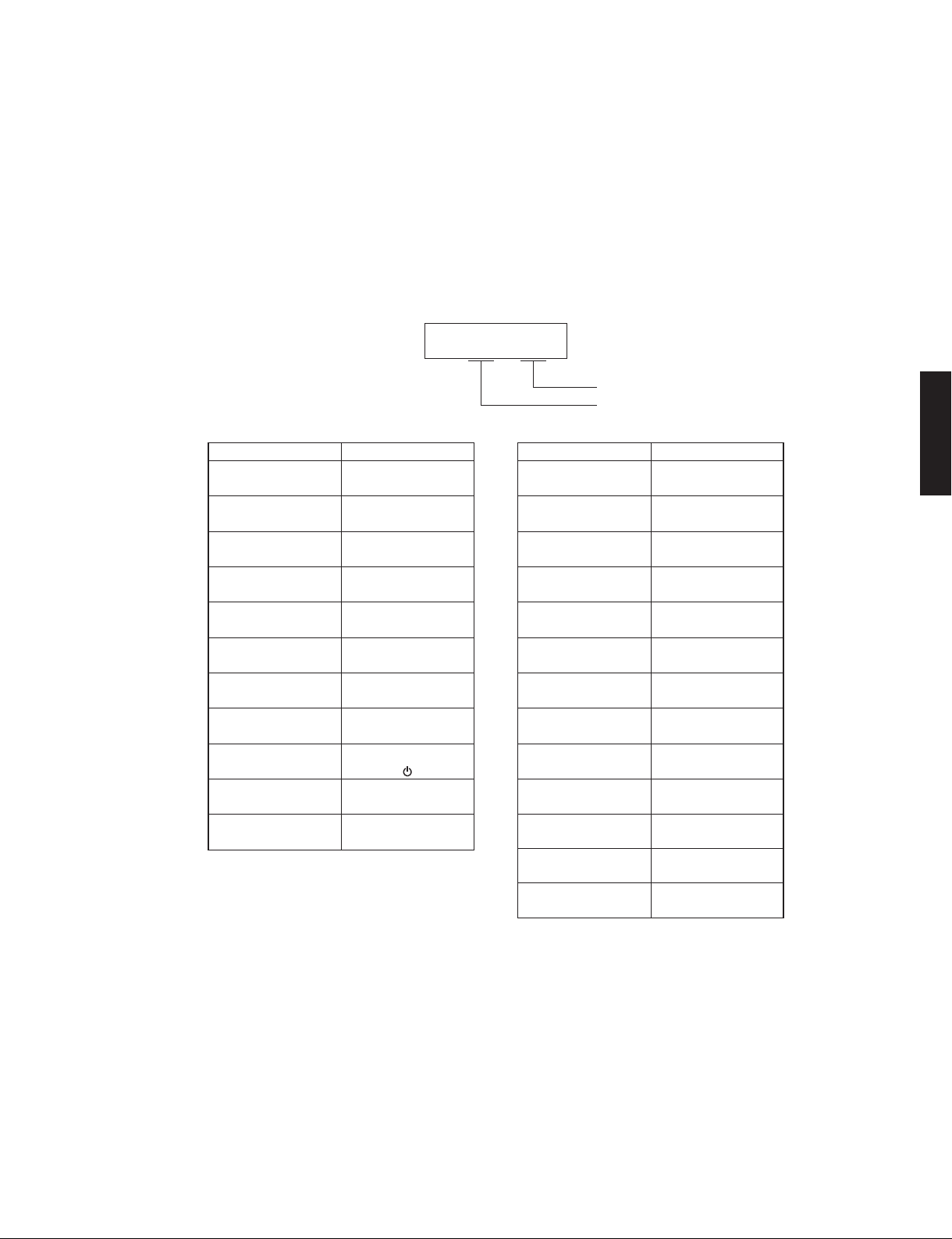
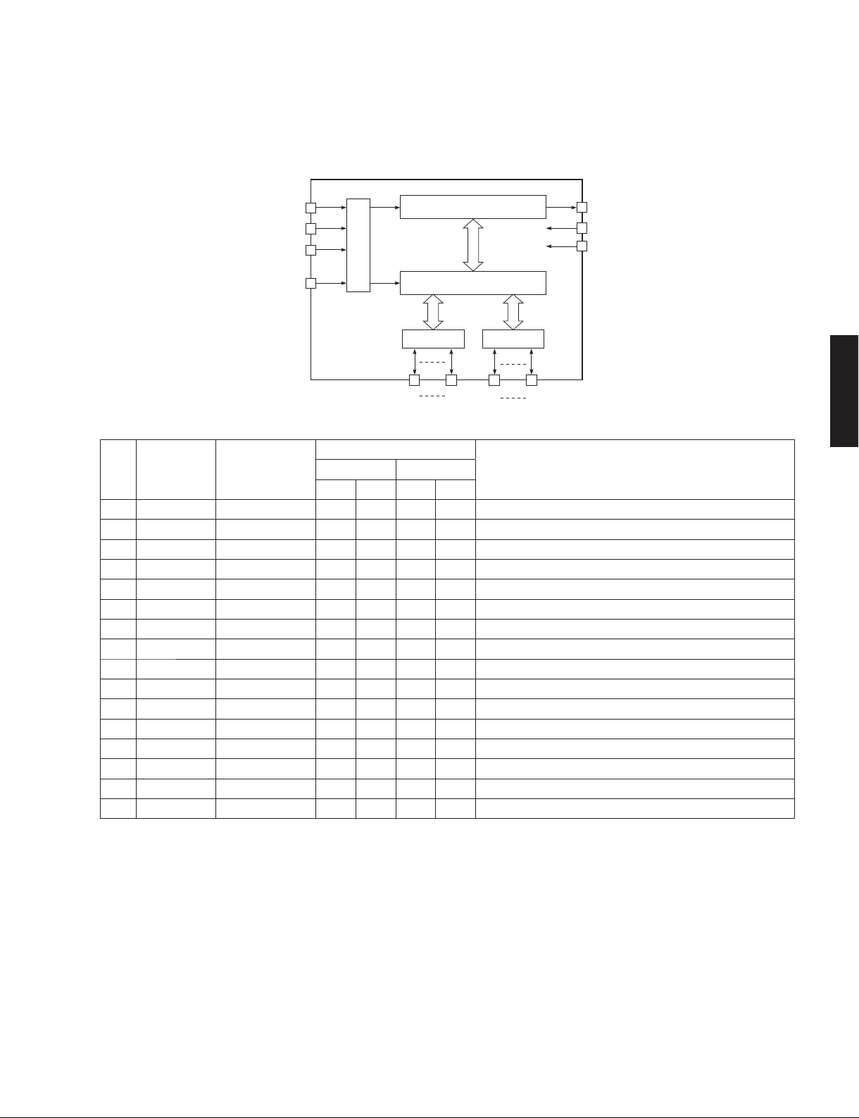
P1. SYSTEM MONITOR
This menu is used to display the A/D conversion value of the microprocessor which detects panel keys and protection
functions by using the sub-menu.
When “P1-7. KEY1/KEY2” sub-menu is selected, keys become non-operable due to detection of the values of all keys.
However, it is possible to advance to the next sub-menu by pressing the “SCENE RADIO” (forward) key or “SCENE
CD” (reverse) key on the remote control.
* Numeric values in the figure are given as reference only.
P1-1. DC
Power amplifier DC (DC voltage) output is detected.
The voltage at 5 pin (DC_PRT) of IC89 is displayed.
Normal value: 35 to 68
(Reference voltage: 3.3 V=255)
* If DC becomes out of the normal value range, the protection function works to turn off the power.
P1 1
DC:51
RX-V671/HTR-6064/
RX-A710
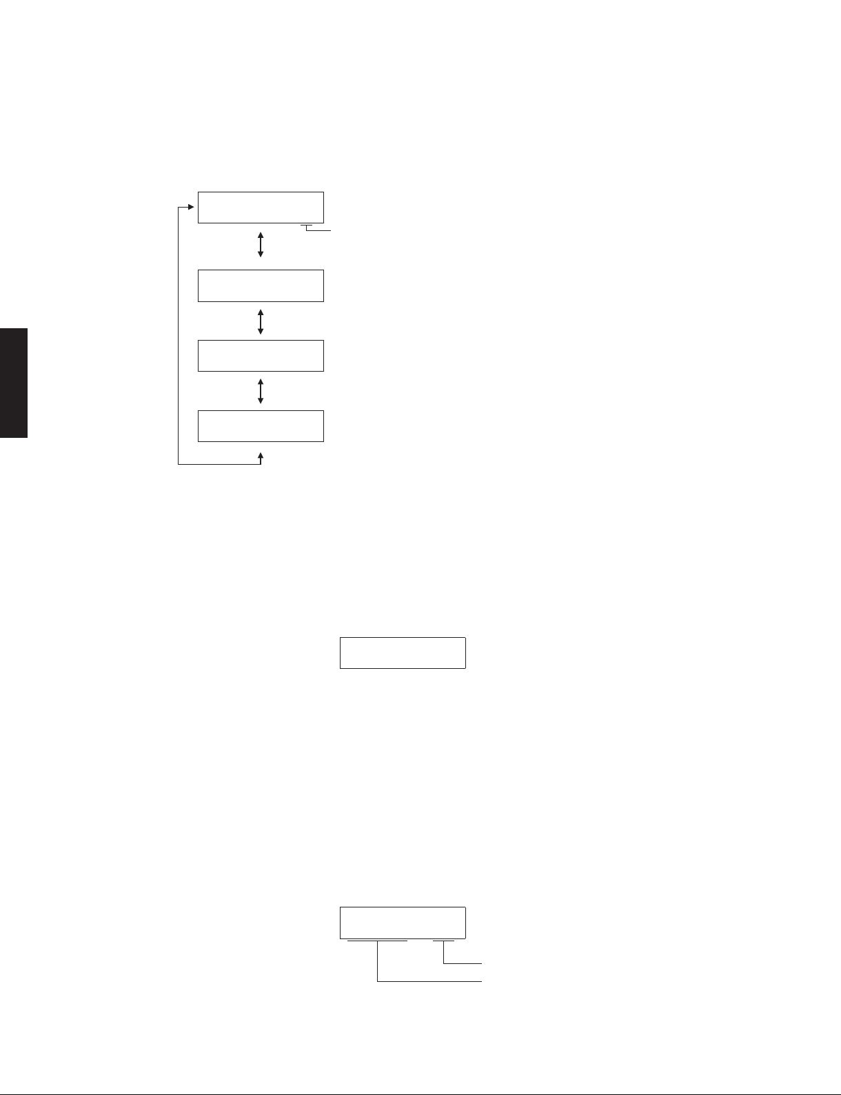
P1-2. PS1/PS2
Power supply voltage protection detection
The voltage at 2 pin (PS1_PRT)/1 pin (PS2_PRT) of IC89 are displayed.
Voltage detects
PS1: ACBL, AC12, AC5, ±7, +3.3s, -5VA
PS2: -VP, +5T, +5A, +3.3s
Normal value
PS1: 33 to 128
PS2: 90 to 166 (±5VA: On)
143 to 220 (±5VA: Off)
(Reference voltage: 3.3 V=255)
* If PS1 or PS2 becomes out of the normal value range, the protection function works to turn off the power.
P1 2
PS:80/128
P1-3. TM
Temperature of the heatsink is detected.
The voltage at 12 pin (TMH1) of IC89 is displayed.
Normal value: 42 to 255
(Reference voltage: 3.3 V=255)
* If TM becomes out of the normal value range, the protection function works to turn off the power.
P1 3
TMa:109
61
Page 2

RX-V671/HTR-6064/RX-A710
P1-4. INVALID ITEM
Not for service.
P1-5. OUTPUT LEVEL
Output level of speaker output is detected.
The voltage at 165 pin (AMP_OLV) of IC89 is displayed.
(Reference voltage: 3.3 V=255)
RX-A710
P1 4
INVALIDITEM
P1 5
OUTLVL:255
RX-V671/HTR-6064/
P1-6. LIMITER CONTROL
P1-7. L3 (J model)
Power limitter control is detected.
The voltage at 4 pin (AMP_LMT) of IC81 is displayed.
(Reference voltage: 3.3 V=255)
P1 6
LMTCNT:255
Not for service.
P1 7
L3:11
62
Page 3
RX-V671/HTR-6064/RX-A710
P1-7. KEY1/KEY2
Panel key is detected.
When the A/D conversion value of the panel key becomes out of the specified range, normal operation will not
be available.
In that case, check the constant of voltage dividing resistor, solder condition, etc. Refer to table.
* When “P1-7. KEY1/KEY2” menu is selected, keys become non-operable due to detection of the values of all
keys. However, it is possible to advance to the next sub-menu by pressing the “SCENE RADIO” (forward)
key or “SCENE CD” (reverse) key on the remote control.
(Reference voltage: 3.3 V=255)
P1 7
KY:255/255
KEY2
KEY1
RX-V671/HTR-6064/
RX-A710
Display KEY1
0 – 11
12 – 32
33 – 54
55 – 75
76 – 96
97 – 119
120 – 142
143 – 172
173 – 202
203 – 235
255 Key off
RADIO
(SCENE4)
CD
(SCENE3)
TV
(SCENE2)
BD/DVD
(SCENE1)
ZONE2
CONTROL
ZONE2
ON/OFF
INPUT
INPUT
MAIN ZONE
TONE
CONTROL
Display KEY2
0 – 11
12 – 32
33 – 54
55 – 77 AM
78 – 99 FM
100 – 121
>
<
122 – 144
145 – 166 MEMORY
167 – 186 INFO
187 – 205 STRAIGHT
206 – 226
227 – 246
255 Key off
PURE
DIRECT
TUNING
>>
TUNING
<<
PRESET
>
PRESET
<
PROGRAM
>
PROGRAM
<
63
Page 4
RX-V671/HTR-6064/RX-A710
P2. PROTECTION HISTORY
This menu is used to display the history of protection function.
All history of protection function will be erased by pressing the “STRAIGHT” key.
* Numeric values in the figure are given as reference only.
RX-A710
RX-V671/HTR-6064/
S1. F/W UPDATE
Not for service.
P2 1
2nd:PS280
P2 2
1st:TMP10
P2 3
3th:DC0
P2 4
NoPrt
P2-1. History 1
A/D conversion value when the protection function is activated.
(Reference voltage: 3.3 V=255)
P2-2. History 2
P2-3. History 3
P2-4. History 4
S1 1
F/WUPDATE?
S2. SET INFORMATION
The model name and destination of this unit are displayed.
S2-1. MODEL
The model name of this unit is displayed.
S2 1
MDL:V671255
Not for service.
Model name
V671 : RX-V671
6064 : HTR-6064
A710 : RX-A710
64
Page 5
RX-V671/HTR-6064/RX-A710
S2-2. DESTINATION
The destination of this unit is displayed.
S2 2
DEST:U28
A/D conversion value
Destination
Destination J U C R, S T K A B, G, F L
A/D conversion value
(3.3 V=255)
0 − 12 13 − 39 40 − 67 68 − 92 93 − 115 116 − 140 141 − 169 199 − 221 222 − 244
S2-3. DEBUG
Not for service.
S2 3
DBG:255
RX-V671/HTR-6064/
RX-A710
S3. FACTORY PRESET
This menu is used to reserve/inhibit initialization of the back-up IC (EEPROM: IC83 on DIGITAL P.C.B.).
S3 1
PRESET:INH
S3 1
PRESET:RSRV
CAUTION: Before setting to the PRESET RESERVED, write down the existing preset memory content of the tuner. (This is
because setting to the PRESET RESERVED will cause the user memory content to be erased.)
S3-1. PRESET INHIBIT (Initialization inhibited)
Initialization of the back-up IC is not executed. Select this sub-menu to protect the values set by the user.
S3-1. PRESET RESERVED (Initialization reserved)
Initialization of the back-up IC is reserved. (Actual initialization is executed the next time the power is
turned on.) To reset to the original factory settings or to reset the backup IC, select this sub-menu and
press the “MAIN ZONE
” key to turn off the power.
65
Page 6
RX-V671/HTR-6064/RX-A710
S4. ROM VERSION/CHECKSUM
The firmware version and checksum values are displayed.
The checksum is obtained by adding the data at every 8-bit and expressing the result as a 4-figure hexadecimal
notation.
* Numeric values in the figure are given as reference only.
S4 1
SYS VER.0.27
S4 2
VER.C0027
RX-A710
RX-V671/HTR-6064/
S4 3
SUM.ECE1
S4 4
FR V.00071
S4 5
FR S.EB01
S4 6
S VER.C0022
S4-1. SYSTEM VERSION
The firmware version is displayed.
S4-2. MICROPROCESSOR VERSION
The firmware version of MICROPROCESSOR (IC81 on DIGITAL P.C.B.) is displayed.
S4-3. MICROPROCESSOR CHECKSUM
The checksum value of MICROPROCESSOR (IC81 on DIGITAL P.C.B.) is displayed.
S4-4. FLASH ROM VERSION
The firmware version of FLASH ROM (IC82 on DIGITAL P.C.B.) is displayed.
S4-5. FLASH ROM CHECKSUM
The checksum value of FLASH ROM (IC82 on DIGITAL P.C.B.) is displayed.
S4-6. BF (NETWORK microprocessor) VERSION
The firmware version of BF (NETWORK microprocessor, IC901 on DIGITAL P.C.B.) is displayed.
66
S4 7
S SUM.09452A5F
S4 8
D1 V.1.01r1
S4 9
D1 S.71616BDC
S4 10
INVALIDITEM
S4-7. BF (NETWORK microprocessor) CHECKSUM
The checksum value of BF (NETWORK microprocessor, IC901 on DIGITAL P.C.B.) is displayed.
S4-8. DSP1 VERSION
The firmware version of DSP1 (IC921 on DIGITAL P.C.B.) is displayed.
S4-9. DSP1 CHECKSUM
The checksum value of DSP1 (IC921 on DIGITAL P.C.B.) is displayed.
S4-10. INVALID ITEM
Not for service.
Page 7
RX-V671/HTR-6064/RX-A710
S4 11
INVALIDITEM
S4 12
G V.098082142
S4 13
FPGA G V.59
S4 14
FPGA I V.29
S4 15
SRVER.A001
S4 16
INVALIDITEM
S4-11. INVALID ITEM
Not for service.
S4-12. GUI VERSION
The firmware version of GUI data is displayed.
S4-13. FPGA GUI VERSION
The firmware version of GUI section in FPGA (IC51 on DIGITAL P.C.B.) is displayed.
S4-14. FPGA IP VERSION
The firmware version of video processor section in FPGA (IC51 on DIGITAL P.C.B.) is displayed.
S4-15. SIRIUS VERSION (U model)
The firmware version of SIRIUS is displayed.
S4-16. INVALID ITEM
Not for service.
RX-V671/HTR-6064/
RX-A710
S4 17
HDR.A001
S4-17. HD RADIO VERSION (U model)
The firmware version of HD radio is displayed.
67
Page 8
RX-V671/HTR-6064/RX-A710
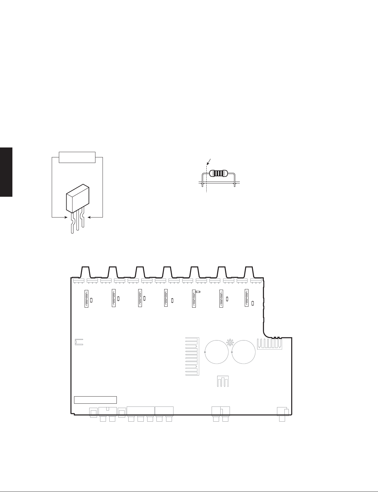
■ CONFIRMATION OF IDLING CURRENT OF AMP UNIT
● Right after power is turned on, confirm that the voltage across the terminals of R1152 (SURROUND BACK Rch), R1154
(SURROUND Rch), R1150 (FRONT Rch), R1148 (CENTER), R1149 (FRONT Lch), R1153 (SURROUND Lch), R1151
(SURROUND BACK Lch) are between 0.1 mV and 10.0 mV.
● If it exceeds 10.0 mV, open (cut off) R1090 (SURROUND BACK Rch), R1092 (SURROUND Rch), R1088 (FRONT Rch),
R1086 (CENTER), R1087 (FRONT Lch), R1091 (SURROUND Lch), R1089 (SURROUND BACK Lch) and reconfirm the
voltage.
Attention
If the measured voltage exceeds 10.0 mV after an amplifier repair, first check for a defective component before cutting
the bias resistor.
● Confirm that the voltage is 0.2 mV to 15.0 mV after 60 minutes.
RX-A710
RX-V671/HTR-6064/
0.1 mV – 10.0 mV
(DC)
R1154 R1153 R1152 R1151 R1150 R1149 R1148
Open (cut off)
R1152 (SURROUND BACK Rch)
R1154 (SURROUND Rch)
R1150 (FRONT Rch)
R1148 (CENTER)
R1149 (FRONT Lch)
R1153 (SURROUND Lch)
R1151 (SURROUND BACK Lch)
Front side
R1092 R1091 R1090 R1089 R1088 R1087
R1090 (SURROUND BACK Rch)
R1092 (SURROUND Rch)
R1088 (FRONT Rch)
R1086 (CENTER)
R1087 (FRONT Lch)
R1091 (SURROUND Lch)
R1089 (SURROUND BACK Lch)
R1086
68
MAIN (1) P.C.B.
Page 9
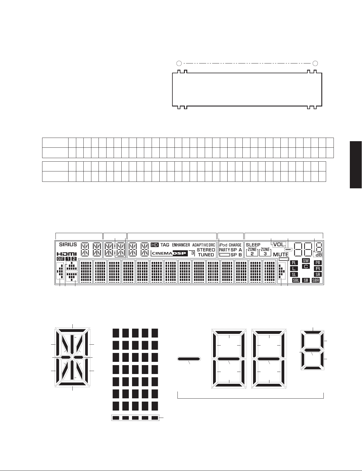
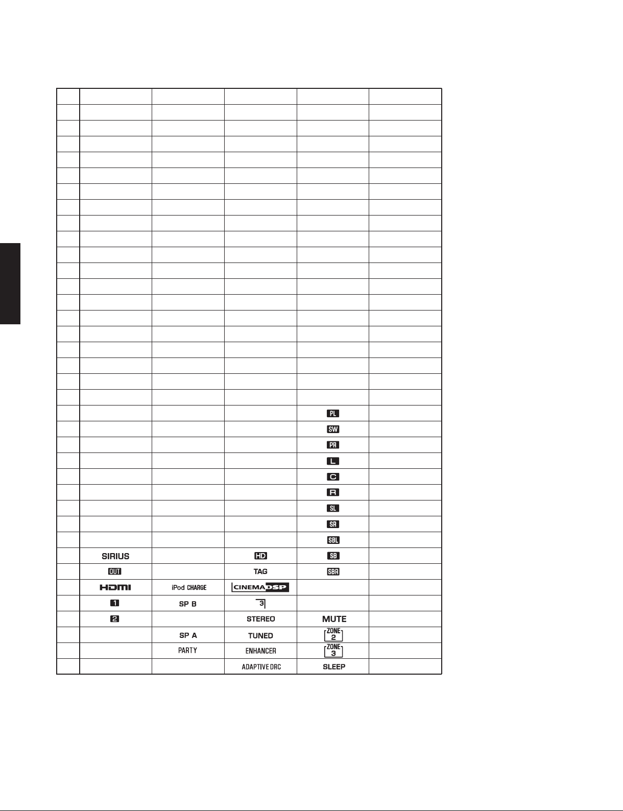
■ DISPLAY DATA
● V4001 : HNA-18MM03T (OPERATION P.C.B.)
RX-V671/HTR-6064/RX-A710
69
PATTERN AREA
● PIN CONNECTION
Pin No.
Connection
Pin No.
Connection
Note : 1) F1, F2 ..... Filament pin 2) 1G–18G ..... Grid pin 3) P1–P36 ..... Anode pin 4) NP ..... No pin 5) NX ..... No extended pin
● GRID ASSIGNMENT
69
68 67NP66NP65P164P263P362P461P560P659P758P857P956
F2 F2
34
P3233P3332P3431P3530P36
18G
1a 1a1a2a 2a2a
29 28
NXNX27NX26NX25NX24NX23NX2218G2117G2016G1915G1814G1713G1612G1511 G1410G139G128G117G106G95G84G73G62G51G4NP3NP
17G
3a 3b
P1055P1154P1253P1352P1451P1550P1649P1748P1847P1946P2045P2144P2243P2342P2441P2540P2639P2738P2837P29
16G
17G
15G
1
36
P3035P31
RX-V671/HTR-6064/
RX-A710
21
F1F1
V1 S1S3 S1
A1
A3
A2
a
j
f
h
gm
e
p
d
(18G–16G)
2G1G 3G 4G 5G 6G 7G 11G10G9G8G 12G 13G 14G
1-1 2-1 3-1 4-1 5-1
1- 2
b
k
nr
c
2-2
1- 3
2-3
1- 4
2-4
1- 5
2-5
1- 6
2-6
1- 7
2-7
(1G–14G)
3-2
3-3
3-4
3-5
3-6
3-7
4-2
4-3
4-4
4-5
4-6
4-7
5-2
5-3
5-4
5-5
5-6
5-7
U1
V2
V7V6V3
V8V1
V5
S2
A4
V18
V9
V14
V10
V17
V15
V4
V13
V11
V12
V16
V17
V18
(15G)
69
Page 10
RX-V671/HTR-6064/RX-A710
● ANODE CONNECTION
P1
P2
P3
P4
P5
P6
P7
P8
P9
P10
P11
P12
RX-A710
RX-V671/HTR-6064/
P13
P14
P15
P16
P17
P18
P19
P20
P21
P22
P23
P24
P25
P26
P27
P28
P29
P30
P31
P32
P33
P34
P35
P36
18G
1a
1h
1j
1k
1b
1f
1m
1g
1c
1e
1r
1p
1n
1d
2a
2h
2j
2k
2b
2f
2m
2g
2c
2e
2r
2p
2n
2d
A1
A2
A3
17G
1a
1h
1j
1k
1b
1f
1m
1g
1c
1e
1r
1p
1n
1d
2a
2h
2j
2k
2b
2f
2m
2g
2c
2e
2r
2p
2n
2d
3a
3b
S3
–
16G
1a
1h
1j
1k
1b
1f
1m
1g
1c
1e
1r
1p
1n
1d
2a
2h
2j
2k
2b
2f
2m
2g
2c
2e
2r
2p
2n
2d
15G
S1
V1
V5
V12
V18
V6
V13
V17
V4
V11
V16
V8
V15
V7
V14
V3
V10
V2
V9
A4
S2
1G–14G
1-1
2-1
3-1
4-1
5-1
1-2
2-2
3-2
4-2
5-2
1-3
2-3
3-3
4-3
5-3
1-4
2-4
3-4
4-4
5-4
1-5
2-5
3-5
4-5
5-5
1-6
2-6
3-6
4-6
5-6
1-7
2-7
3-7
4-7
5-7
U1
70
Page 11
■ IC DATA
IC81: R5F6416MADFE (DIGITAL P.C.B.)
Microprocessor
* No replacement part available.
RX-V671/HTR-6064/RX-A710
8 8 8 8 8 8 8
Port P0 Port P1 Port P2 Port P3 Port P4 Port P5 Port P6
Peripheral functions
Timer A16 bits × 5 timers
Timer B16 bits × 6 timers
Three-phase motor
Serial interface:
Multi-master I2C-bus
Intelligent I/O
Time Measurement: 16
Wave generation: 24
Serial interface:
- Variable-length
synchronous serial I/O
- IEBus
Port P19
8
Timer:
controller
11
channels
interface:
1 channel
Port P18
Port P17
8
A/D converter:
10 bits × 1 circuit
Standard: 10 inputs
Maximum: 34 inputs
D/A converter:
8 bits × 2 channels
X-Y converter:
16 bits × 16 bits
CRC calculator (CCITT)
16
12
X
+ X
+ X5 + 1
R32C/100 Series Microprocessor Core
R2R0
R2R0
R3R1
R6R4
R7R5
A0
A1
A2
A3
FB
SB
8
FLG
INTB
ISP
USP
PC
SVF
SVP
VCT
Port P15Port P16 Port P13Port P14 P14_1
88 85
Clock generator:
4 circuits
- XIN-XOUT
- XCIN-XCOUT
- On-chip oscillator
- PLL frequency synthesizer
Watchdog timer:
15 bits
DMAC
DMAC II
Floating-point unit
Memory
ROM
RAM
Multiplier
Port P7
8
Port P8
7
P8_5 Port P9
8
Port P10
8
Port P11
RX-V671/HTR-6064/
RX-A710
8
Port P12
8
D[8]
D[7]
D[6]
D[5]
D[4]
SV_DET
EEP_N_CS
HP_N_DET
FPGA_N_CS
EEP_MISO
EX_CLK
EX_MOSI
(no_use)
VDEC_N_RST
(no_use)
DAC_N_CS
DIR_N_CS
F_HEQ_CE
D[3]
D[2]
D[1]
D[0]
PS1_PRT
PS2_PRT
DOCK1_ID
THM2
THM1
DSP_MISO
DSP_CLK
VSS
DSP_MOSI
VCC
AMP_OLV
DC_PRT
L3_DET
DEST
MODEL
KY_AD2
KY_AD1
AVSS
TU_N_RST
VREF
AVCC
TU_SCL
D[9]
D[10]
D[11]
D[12]
D[13]
D[14]
D[15]NCA[1]
A[2]
A[3]
A[4]
A[5]
A[6]
A[7]
VSS
A[8]
VCC
USB_SDA
FPGA_CDONE
USB_SCL
FPGA_N_STA
FPGA_N_CFG
A[9]
A[10]
A[11]
HEQ_N_RST
CLK9
RXD9
TXD9
A[12]
A[13]
A[14]
A[15]
HRX_N_RST
HTX_N_RST
DK1_MISO
DK1_MOSI
A[16]
FL_N_CS
DSP_N_INT
VDI_N_MMT
A[17]
FROM_N_RST
USB_SEARCH
133
132
131
130
129
128
127
126
125
124
123
122
121
120
119
118
117
116
115
114
113
112
111
110
109
108
107
106
105
VCC
NMI
104
REM_IN
DIR_N_INT
WAKEUP_INT
134
135
136
137
138
139
140
141
142
143
144
145
146
147
148
149
150
151
152
153
154
155
156
157
158
159
160
161
162
163
164
165
166
167
168
169
170
171
172
173
174
175
176
12345678910111213141516171819202122232425262728293031323334353637383940414243
VDC0
TU_SDA
VOL_CLK
AMP_LMT
VOL_MOSI
HDMI_SDA
FL_N_RST
HDMI_SCL
+3.3S_PON
HDMI_PON
HRX_N_INT
HDMI_MUTE
VOL_RB
VOL_RA
ACPWR_DET
VDC1
IC81
R5F6416MADFE
XIN
DK1_PON
DSP_PON
MCPU_N_RST
XOUT
VSS
NSD
CNVSS
9998979695949392919089
103
102
101
100
I_PRT
HEQ_SCL
TU_N_INT
RWT_CDDA
HEQ_SDA
USB_N_PRT
HTX_AUSEL
A[18]
VIDI2C_ON
A[19]
88
A[20]
87
A[21]
86
A[22]
85
FLASH_N_CS
84
P19_2
83
VID_SEL1
82
VID_SEL2
81
VID_SEL3
80
CPNT_SEL
79
DK1_AP
78
CDDA_DATA
77
DSP_N_SPIRDY/CDDA_WCK
76
DSP_N_CS
75
MCBUS_N_WR/DBG_N_CE
74
NC(BC1)
73
MCBUS_N_RD
72
NC(BCLK)
71
MT_N_5CH
70
MT_N_SW
69
VCC
68
MT_DA
67
VSS
66
MT_N_SB
65
NC
64
DBG_EPM
63
DFF_N_CS
62
NC(RDY)
61
CPNT_N_VMT
60
USB_IPLERR
59
UAW_PON
58
(no_use)
57
(no_use)
56
P19_5
55
USB_MCHNG
54
APL_CLK
53
APL_MISO
52
APL_MOSI
51
DBG_BUSY
50
DBG_CLK
49
MIC_N_DET
48
DBG_MISO
47
STBY_LED
46
DBG_MOSI
45
FPGA_MOSI
44
FPGA_SCL
USB_BUSY
USB_IRPTO
DK1_N_IPDET
71
Page 12
RX-V671/HTR-6064/RX-A710
Pin
No.
SRXD4/SDA4/TXD4/
1
ANEX1/P9_6
2 CLK4/ANEX0/P9_5
N_CTS4/N_N_RTS4/
3
N_SS4/TB4IN/DA1/
P9_4
N_CTS3/N_N_RTS3/
4
N_SS3/TB3IN/DA0/
P9_3
IEOUT/ISTXD2/
OUTC2_0/SRXD3/
5
SDA3/TXD3/TB2IN/
P9_2
IEIN/ISRXD2/STXD3/
6
SCL3/RXD3/TB1IN/
P9_1
7 CLK3/TB0IN/P9_0 SPRY_5CH O H act O Low SP relay 5CH (L, C, R, SRL, SRR)
RX-A710
RX-V671/HTR-6064/
8 P19_7 PA_B_RY O
9 N_INT8/P14_6 HRX_N_INT I L act O Low Interrupt from HDMI RX
10 P19_6 FLD_N_RST O L act O Low FLD reset
11 N_INT7/P14_5 HDMI_MUTE I H act O Low Mute from HDMI RX
12 N_INT6/P14_4 PWR_DET I L act I --- AC power detect
13 P14_3 FLD_N_CS O L act O Low FLD chip select
14 VDC0 VDC0 ---
P14_1 (for exclusive
15
use of the input)
16 VDC1 VDC1 --17 NSD NSD Debugger
18 CNVSS DBG_CNVSS --19 XCIN/P8_7 MIC_N_DET I L act O Low Microphone detection
20 XCOUT/P8_6 PD_LED O H act O Low PURE DIRECT LED
21 RESET MCPU_N_RST --22 XOUT XOUT --23 VSS VSS --24 XIN XIN --25 VCC VCC --26 NMI/P8_5 NMI ---
27 N_INT2/P8_4 WAKEUP_INT I
28 N_INT1/P8_3 REM_IN2 I L act O Low Remote control pulse input 2
29 N_INT0/P8_2 REM_IN1 I L act O Low Remote control pulse input 1
UD0B/UD1B/IIO1_5/
30
N_RTS5/N_CTS5/N_
SS5/U/TA4IN/P8_1
UD0A/UD1A/RXD5/
31
SCL5/S
TA4OUT/P8_0
32 P18_1 FLD_PON O H act O Low FL driver +3.3V power supply control
33 P18_0 STBY_LED O H act O Low Standby LED control
UD0B/UD1B/IIO1_4/
34
CLK5/TA3IN/P7_7
UD0A/UD1A/IIO1_3/
N_RTS8/N_CTS8/
35
TXD5/SDA5/SRXD5/
TA3OUT/P7_6
IIO1_2/RXD8/W/
36
TA2IN/P7_5
IIO1_1/CLK8/W/
37
TA2OUT/P7_4
38 P17_7 ISEL_RA I I --- Input selector A
39 P17_6 ISEL_RB I I --- Input selector B
40 P17_5 VOL_RA I I --- Volume A
41 P17_4 VOL_RB I I --- Volume B
Port Name Function Name
TUN_SDA I/O Data O Low Tuner I2C data
HDR_MOSI O Data O Low HD Radio transmission data (U model)
VOL1_SCK O Clock O Low VOL1 (R2A15220FP #1) communication clock
VOL_MOSI O Data O Low VOL1/VOL2/VOL3 communication data
AMP_LMT O D/A I --- Limiter control
HDMI_SDA I/O Data O Low HDMI and DVIDEO(AVIDEO:Vx071) 400k I2C data
HDMI_SCL O Clock O Low HDMI and DVIDEO (AVIDEO:Vx071) 400k I2C clock
I_PRT I H act I --- Current protection
TUN_N_INT I L act O Low Interrupt from TUNER
--- O Low O Low No used
TXD5/U/
HEQ_SCL O Clock
DSP1_N_INT I L act O Low Interrupt from DSP1
HEQ_SDA I/O Data O Low HDMI switcher 100k I2C data
DIR_N_INT I L act O Low Interrupt from DIR
IR_CAR O Data O Low Carrier output for SCENE IR (spare)
Related Power Supply
I/O Logic I/O Logic
H : B =
edges
O Low Power amplifier B power supply control
Low
Both
O Low Power switch, MISO interrupt of RS-232C and Dock (Sleep return)
O Low HDMI switcher 100k I2C clock
Detail of FunctionON OFF
72
Page 13
RX-V671/HTR-6064/RX-A710
Pin
No.
42
43
44
45
46
47 P14_7 DSP_PON O H act O Low DSP power supply
48
49 P11_7 DAC_N_CS O L act O Low DAC chip select (SW of V3071, FP DAC is D-FF)
50 CLK1/P6_5 DBG_SCK I Clock O Low E8a
51
52
53
54 TB1IN/CLK0/P6_1 DSP_SCK O Clock O Low DSP/DIR/DAC communication clock
55
56 P19_5 --- I --- I --- No used (+3.3DSP is applied, input por t setting)
57
58
59
60
61 P19_4 EEP_N_CS O L act O Low EEPROM chip select
62
63 ALE/CS2/RXD7/P5_6 DFF2_N_CS B Bus O Low External bus DFF2 chip select
64 HOLD/CLK7/P5_5 DBG_EPM I I --- E8a
65
66
67 VSS VSS ---
68
69 VCC VCC ---
70
71
72 CLKOUT/BCLK/P5_3 NC(BCLK) B Bus O Low External bus
73 RD/P5_2 MCBUS_N_RD B Bus O Low External bus
74 WR1/BC1/P5_1 NC(BC1) B Bus O Low External bus
75 WR0/WR/P5_0
76 D23/P12_7 MT_DA O H act O Low Mute Digital Audio
77 D22/P12_6 DIR_N_CS O L act O Low DIR chip select
78 D21/P12_5 DIR_N_RST O L act O Low DIR reset
Port Name Function Name
IIO1_0/TXD8/N_SS2/
N_RTS2/N_CTS2/V/
TA1IN/P7_3
CLK2/V/TA1OUT/
P7_2
MSCL/IEIN/ISRXD2/
OUTC2_2/IIO1_7/
STXD2/SCL2/RXD2/
TA0IN/TB5IN/P7_1
TA0OUT/TXD2/
SDA2/SRXD2/
IIO1_6/OUTC2_0/
ISTXD2/IEOUT/
MSDA/P7_0
TXD1/SDA1/SRXD1/
P6_7
RXD1/SCL1/STXD1/
P6_6
N_CTS1/N_RTS1/
N_SS1/OUTC2_1/
ISCLK2/P6_4
TXD0/SDA0/SRXD0/
P6_3
TB2IN/RXD0/SCL0/
STXD0/P6_2
TB0IN/N_CTS0/N_
RTS0/N_SS0/P6_0
D31/OUTC2_7/
P13_7
D30/OUTC2_1/
ISCLK2/P13_6
D29/OUTC2_2/ISRXD2/IEIN/P13_5
D28/OUTC2_0/
ISTXD2/IEOUT/
P13_4
RDY/CS3/N_CTS7/
N_RTS7/P5_7
A/CS1/TXD7/
HLD
P5_4
D27/OUTC2_3/
P13_3
D26/OUTC2_6/
P13_2
D25/OUTC2_5/
P13_1
D24/OUTC2_4/
P13_0
DK1_N_IPDET I L act O Low Dock iPod detect
SR_PON O H act O Low SIRIUS power supply control
SR_MISO I Data O Low SIRIUS reception data
SR_MOSI O Data O Low SIRIUS transmission data
232C_DBG_MOSI O Data O Low RS-232C transmission data / Debug / E8a
232C_DBG_MISO I Data O Low RS-232C reception data / Debug / E8a
DBG_BUSY O O Low E8a
DSP_MOSI O Data O Low DSP/DIR/DAC transmission data
DSP_MISO I Data I --- DSP/DIR/DAC reception data
NCPU_N_INT I H act O Low Network microprocessor interrupt
DSP1_N_RST O L act O Low DSP1 reset
EX_SCK O Clock O Low FL/EEPROM/ expansion IO communication clock
EEP_MISO I Data O Low EEPROM reception data
EX_MOSI O Data O Low FL/EEPROM/ expansion IO transmission data
FPGA_N_CS B Bus O Low External bus FPGA chip select
DFF1_N_CS B Bus
DSP1_N_SPIRDY I L act O Low DSP1 SPI ready
DSP2_N_CS O L act O Low DSP2 chip select
DSP1_N_CS O L act O Low DSP1 chip select
MCBUS_N_WR B Bus I --- External bus
DBG_N_CE I I --- E8a
--- O Low O Low No used
Related Power Supply
Detail of FunctionON OFF
I/O Logic I/O Logic
O Low External bus DFF1 chip select
RX-V671/HTR-6064/
RX-A710
73
Page 14
RX-V671/HTR-6064/RX-A710
Pin
No.
79 P19_3 DK1_AP I L act I --- iPod accessory power
80 P17_3 DK1_PON O H act O Low Dock power supply
81 P17_2 UAW_PON O H act O Low UAW power supply control
82 P17_1 NCPU_PON O H act O Low NET/USB power supply
83 P17_0 NET_SEL_M O H NET O Low Main USB/NET select
84 P19_2 NET_SEL_Z O H NET O Low Zone USB/NET select
CS0/A23/TXD6/
85
SDA6/SRXD6/P4_7
CS1/A22/RXD6/
86
SCL6/STXD6/P4_6
87 CS2/A21/CLK6/P4_5 A[21] B Bus O Low External bus
CS3/A20/N_CTS6/N_
88
RTS6/N_SS6/P4_4
A19/TXD3/SDA3/
89
SRXD3/OUTC2_0/
ISTXD2/IEOUT/P4_3
90 P11_6 --- O Low O Low Spare
A18/RXD3/SCL3/
91
RX-A710
RX-V671/HTR-6064/
STXD3/ISRXD2/IEIN/
P4_2
92 P11_5 --- O Low O Low Spare
93 A17/CLK3/P4_1 A[17] B Bus O Low External bus
A16/N_CTS3/N_
94
RTS3/N_SS3/P4_0
95 P16_7/TXD10 DK_MOSI O Data O Low Dock UART transmission data
96 P16_6/RXD10 DK_MISO I Data I --- Dock UART reception data (3.3V logic input)
97 P16_5/CLK10 R32C_N_INT O L act O Low Interrupt of R32C to Blackfin
P16_4/N_CTS10/N_
98
RTS10
A15/[A15/D15]/TA4IN/
99
U/P3_7
A14/[A14/D14]/
100
TA4OUT/U/P3_6
A13/[A13/D13]/TA2IN/
101
W/P3_5
A12/[A12/D12]/
102
TA2OUT/W/P3_4
103 P16_3/TXD9 NCPU_PIC_MISO O Data O Low Network microprocessor SPI transmission data
104 P16_2/RXD9 NCPU_PIC_MOSI I Data O Low Net work microprocessor SPI reception data
105 P16_1/CLK9 NCPU_PIC_SCK I Clock O Low Network microprocessor SPI communication clock
P16_0/N_CTS9/N_
106
RTS9
A11/[A11/D11]/TA1IN/
107
V/P3_3
A10/[A10/D10]/
108
TA1OUT/V/P3_2
A9/[A9/D9]/TA3OUT/
109
UD0B/UD1B/P3_1
110 D20/P12_4 --- O Low O Low Spare
D19/N_CTS6/N_
111
RTS6/N_SS6/P12_3
D18/RXD6/SCL6/
112
STXD6/P12_2
113 D17/CLK6/P12_1 FPGA_SCK O Clock O Low FPGA clock (at Boot)
D16/TXD6/SDA6/
114
SRXD6/P12_0
115 VCC VCC ---
A8/[A8/D8]/TA0OUT/
116
UD0A/UD1A/P3_0
117 VSS VSS ---
A7/[A7/D7]/AN2_7/
118
P2_7/TXD10
A6/[A6/D6]/AN2_6/
119
P2_6/RXD10
A5/[A5/D5]/AN2_5/
120
P2_5/CLK10
Port Name Function Name
FLASH_N_CS O L act O Low External bus Flash ROM chip select
A[22] B Bus O Low External bus
A[20] B Bus O Low External bus
A[19] B Bus O Low External bus
A[18] B Bus O Low External bus
A[16] B Bus O Low External bus
BF_MT I H act O Low Mute signal from Blackfin (NCPU_N_INT distinction use)
A[15] B Bus O Low External bus
4] B Bus
A[1
A[13] B Bus O Low External bus
A[12] B Bus O Low External bus
NCPU_N_RST O L act O Low Network microprocessor reset
A[11] B Bus O Low External bus
A[10] B Bus O Low External bus
A[9] B Bus O Low External bus
--- O Low O Low Spare
--- O Low O Low Spare (After FPGA Config, I2C is possible)
FPGA_MOSI O Data O Low FPGA transmission data (at Boot)
A[8] B Bus O Low External bus
A[7] B Bus O Low External bus
A[6] B Bus O Low External bus
A[5] B Bus O Low External bus
Related Power Supply
Detail of FunctionON OFF
I/O Logic I/O Logic
O Low External bus
74
Page 15
RX-V671/HTR-6064/RX-A710
Pin
No.
121
122
123
124
125
126
127
128
129
130
131
132
13
134 AN0_7/D7/P0_7 D[7] B Bus I --- External bus
135 AN0_6/D6/P0_6 D[6] B Bus I --- External bus
136 AN0_5/D5/P0_5 D[5] B Bus I --- External bus
137 AN0_4/D4/P0_4 D[4] B Bus I --- External bus
138 P19_1 FPGA_N_CFG O L act O Low FPGA nCONF
139 WR3/BC3/P11_4 FPGA_N_STA I L act I --- FPGA nSTATUS
140 P19_0 FPGA_CDONE I H act I --- FPGA CONF DONE
141
142
143
144
145 P18_7 HPRY O H act O Low HP relay
146 P18_6 MT_N_Z2 O L act O Low Mute Zone2 (Line out)
147 P18_5 --- O H act O Low No used
148 P18_4 MT_N_5CH O L act O Low Mute 5ch (L, C, R, SRL, SRR Preout/Main amplifier input)
149 P18_3 MT_N_SW O L act O Low Mute Subwoofer (Preout)
150 P18_2 MT_N_SB O L act O Low Mute SB/BA/Z2/FP (Preout/Main amplifier input)
151 AN0_3/D3/P0_3 D[3] B Bus I --- External bus
152 AN0_2/D2/P0_2 D[2] B Bus I --- External bus
153 AN0_1/D1/P0_1 D[1] B Bus I --- External bus
154 AN0_0/D0/P0_0 D[0] B Bus I --- External bus
155
156
157
Port Name Function Name
A4/[A4/D4]/AN2_4/
P2_4/N_CTS10/N_
RTS10
A3/[A3/D3]/AN2_3/
P2_3/TXD9
A2/[A2/D2]/AN2_2/
P2_2/RXD9
A1/[A1/D1]/BC2/
[BC2/D1]/AN2_1/
P2_1/CLK9
A0/[A0/D0]/BC0/
[BC0/D0]/AN2_0/
P2_0/N_CTS9/N_
RTS9
D15/N_INT5/IIO0_7/
IIO1_7/P1_7
D14/N_INT4/IIO0_6/
IIO1_6/P1_6
D13/N_INT3/IIO0_5/
IIO1_5/P1_5
D12/IIO0_4/IIO1_4/
P1_4
D11/IIO0_3/IIO1_3/
P1_3
D10/IIO0_2/IIO1_2/
P1_2
D9/IIO0_1/IIO1_1/
P1_1
IIO0_0/IIO1_0/D8/
3
P1_0
IIO1_3/N_RTS8/N_
CTS8/WR2/CS3/
P11_3
IIO1_2/RXD8/CS2/
P11_2
IIO1_1/CLK8/CS1/
P11_1
IIO1_0/TXD8/CS0/
P11_0
IIO0_7/N_R
N_CTS6/N_SS6/
AN15_7/P15_7
IIO0_6/CLK6/
AN15_6/P15_6
IIO0_5/RXD6/SCL6/
STXD6/AN15_5/
P15_5
TS6/
A[4] B Bus O Low External bus
A[3] B Bus O Low External bus
A[2] B Bus O Low External bus
A[1] B Bus O Low External bus
A[0] B Bus O Low External bus
D[15] B Bus I --- External bus
D[14] B Bus I --- External bus
D[13] B Bus I --- External bus
D[12] B Bus I --- External bus
D[11] B Bus I --- External bus
D[10] B Bus I --- External bus
D[9] B Bus I --- External bus
D[8] B Bus
NCPU_MISO I Data O Low Network microprocessor UART reception data
SPRY_Z2&FP O H act O Low SP relay Zone2 and Front Presence
NCPU_MOSI O Data O Low Network microprocessor UART transmission data
SVID_DET I
HP_N_DET I L act O Low Headphone detection
EX1_N_CS O L act O Low Expansion IO 1 chip select
--- O Low O Low No used
Related Power Supply
Detail of FunctionON OFF
I/O Logic I/O Logic
I --- External bus
H act I --- S-video detect
RX-V671/HTR-6064/
RX-A710
75
Page 16
RX-V671/HTR-6064/RX-A710
Pin
No.
IIO0_4/TXD6/SDA6/
158
SRXD6/AN15_4/
P15_4
IIO0_3/N_RTS7/N_
159
CTS7/AN15_3/P15_3
IIO0_2/RXD7/
160
AN15_2/P15_2
IIO0_1/CLK7/
161
AN15_1/P15_1
162 VSS VSS ---
IIO0_0/TXD7/
163
AN15_0/P15_0
164 VCC VCC --165 KI3/AN_7/P10_7 +3.3S_PON O H act O Low +3.3S power supply
166 KI2/AN_6/P10_6 --- I A/D O Low No used
167 KI1/AN_5/P10_5 AD1_COM I A/D O Low AD selector 1 COM input
168 KI0/AN_4/P10_4 DEST I A/D O Low Destination distinction
169 AN_3/P10_3 MODEL I A/D O Low Model distinction
RX-A710
RX-V671/HTR-6064/
170 AN_2/P10_2 KY_AD2 I A/D O Low Key 2
171 AN_1/P10_1 KY_AD1 I A/D O Low Key 1
172 AVSS AVSS ---
173 AN_0/P10_0
174 VREF VREF --175 AVCC AVC C ---
STXD4/SCL4/RXD4/
176
ADTRG/P9_7
Port Name Function Name
EX1_N_RST O L act O Low Expansion IO 1 reset
AD_SEL_A O O Low AD select A
AD_SEL_B O O Low AD select B
IR_OUT O Data O Low Remote control cord output
AD_SEL_C O O Low AD select C
TUN_N_RST O L act O Low Tuner reset
HDR_N_RST O L act O Low HD Radio reset (U model)
TUN_SCL O Data O Low Tuner I2C clock
HDR_MISO I Data O Low HD Radio reception data (U model)
Related Power Supply
Detail of FunctionON OFF
I/O Logic I/O Logic
Key detection for A/D port
Key input (A/D) pull-up resistance 10 k-ohms
Ohm 0 + 1.0 k + 1.0 k + 1.5 k + 1.5 k + 2.2 k 22.0 k 33.0 k
V 0 – 0.15 0.15 – 0.42 0.43 – 0.70 0.71 – 0.97 0.98 – 1.24 1.25 – 1.53 2.23 – 2.62 2.63 – 3.04
A/D conversion value
(3.3 V=255)
KEY1 (171 pin)
Ohm 0 + 1.0 k + 1.0 k + 1.5 k + 1.8 k + 2.2 k + 3.3 k + 4.7 k + 6.8 k + 10.0 k
V 0 – 0.15 0.16 – 0.42 0.43 – 0.70 0.71 – 0.99 1.00 – 1.27 1.28 – 1.56 1.57 – 1.86 1.87 – 2.14 2.15 – 2.39 2.40 – 2.65
A/D conversion value
(3.3 V=255)
KEY2 (170 pin) PURE DIRECT
0 – 11 12 – 32 33 – 54 55 – 75 76 – 96 97 – 119 182 – 197 198 – 209
RADIO
(SCENE4)CD(SCENE3)TV(SCENE2)
0 – 11 12 – 32 33 – 54 55 – 77 78 – 99 100 – 121 122 – 144 145 – 166 167 – 186 187 – 205
TUNING
>>
TUNING
<<
BD/DVD
(SCENE1)
AM FM
ZONE2
CONTROL
ZONE2
ON/OFF
PRESET
>
MAIN ZONE
(power)
PRESET
<
TONE
CONTROL
MEMORY INFO STRAIGHT
Destination detection for AD port
Pull-up resistance 10 k-ohms
R3809
(VIDEO P.C.B.)
V 0 – 0.16 0.17 – 0.51 0.52 – 0.87 0.88 – 1.92 1.93 – 1.49 1.50 – 1.81 1.82 – 2.35 2.36 – 2.86 2.87 – 3.15
A/D conversion value
(3.3V=255)
Destination
(168 pin)
0 1.2 k 2.7 k 4.7 k 6.8 k 10.0 k 15.0 k 47.0 k 100.0 k
0 – 12 13 – 39 40 – 67 68 – 92 93 – 115 116 – 140 141 – 169 199 – 221 222 – 244
J U C R, S T K A B, G, F L
76
Page 17
• Microprocessor extended port
IC84, 85: TC74VHC273FT (DIGITAL P.C.B.)
Octal D-type flip-flop with clear
RX-V671/HTR-6064/RX-A710
1CLR
2
Q1
D1
3
D2
4
5
Q2
6
Q3
7
D3
D4
8
9
Q4
10
GND
Inputs Output
DCKCLR
XX
L
L
H
H
H
X
H
20 V
CC
19
Q8
D8
18
D7
17
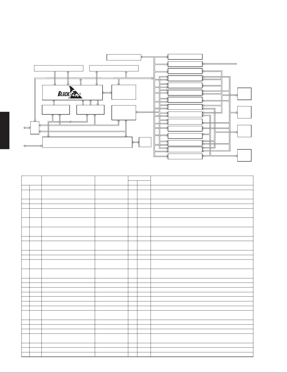
16
Q7
15
Q6
14
D6
D5
13
12
Q5
CK
11
Q
L
Function
Clear
L
H
Q
No Change
n
CLR
CK
−
−
D1
3
1
11
D2
4
R
D
Q
CK
2
Q1
D3
7
R
D
Q
CK
5
Q2
D4
8
R
D
Q
CK
6
Q3
D5
13
R
D
Q
CK
9
Q4
D6
14
R
D
Q
CK
12
Q5
D7
17
R
D
CK
R
D
Q
Q
CK
15
Q6
IC84 (D-FF12)
Pin
R32C external
No.
bus data
Function Name
2 D[8] HDMI_PON O H act O Low HDMI power supply (Necessary for DSP, AVIDEO drive)
5 D[9] HRX_N_RST O L act O Low HDMI RX reset
6 D[10] HTX1_N_RST O L act O Low HDMI TX reset
9 D[11] HTX2_N_RST O L act O Low HDMI TX2 reset
12 D[12] FROM_N_RST O L act O Low FLASH reset
15 D[13] HTX_AUSEL O H HRX O Low HDMI TX sound select
16 D[14] HAU_N_OE O L act O Low HDMI to DIR sound output enable
19 D[15] VIDI2C_ON O H act O Low I2C line switch to video device
Related Power Supply
Detail of FunctionON OFF
I/O Logic I/O Logic
D8
18
R
D
Q
CK
RX-V671/HTR-6064/
16
19
Q7
Q8
RX-A710
IC85 (D-FF11)
Pin
R32C external
No.
bus data
Function Name
2 D[0] HEQ_N_RST O L act O Low HDMI switcher reset
5 D[1] VDEC_N_RST O L act O Low Video decoder reset
6 D[2] USB_OC_FLG O H act O Low USB overcurrent detection flag R32C to BF
9 D[3] HRX_VSEL O L DEC O Low Video decoder to scaler line enable
12 D[4] F_HEQ_CE O H act O Low Front HDMI EQ chip enable
15 D[5] VID_PON O H act O Low Video power supply
16 D[6] +3.3D_PON O H act O Low OR of HDMI_PON, DSP_PON, NET_USB_PON
19 D[7] PRY O H act O Low Power relay
Related Power Supply
Detail of FunctionON OFF
I/O Logic I/O Logic
77
Page 18
RX-V671/HTR-6064/RX-A710
IC89: SN74LV4051APWR (DIGITAL P.C.B.)
8-channel analog multiplexers/demultiplexers
1
16
Y4
2
Y6
3
COM
4
Y7
5
Y5
6
INH
7
GND
8
GND
RX-A710
V
CC
15
Y2
14
Y1
13
Y0
12
Y3
11
A
10
B
9
C
INH
3
COM
13
Y0
14
Y1
15
Y2
12
Y3
1
Y4
5
Y5
2
Y6
4
Y7
L
H
L
H
L
H
L
H
X
ON
CHANNEL
Y0
Y1
Y2
Y3
Y4
Y5
Y6
Y7
None
INH
11
A
10
B
9
C
6
INPUTS
BA
C
L
L
L
L
L
L
L
L
L
L
L
H
L
L
H
L
H
H
L
H
L
H
H
H
H
X
X
RX-V671/HTR-6064/
Pin
No.
AD selector 1 (AD1_COM signal is input into AN_5 of R32C)
1 Y4 PS2_PRT I A/D I --- Power supply protection 2
2 Y6 PS1_PRT I A/D I --- Power supply protection 1
4 Y7 AMP_OLV I A/D I --- Amplifier output level detection
5 Y5 DC_PRT I A/D I --- DC protection
12 Y3 THM1 I A/D I --- Temperature detection 1
13 Y0 DK1_ID I A/D I --- Dock ID detection
14 Y1 L3_DET I A/D I --- D terminal L3 detection
15 Y2 MODE I A/D I --- Special mode distinction
DOCK detection for AD port
Pull-up resistance 10 k-ohms
DOCK type Bluetooth Wireless iPod iPod
(DKID 13 pin) (YBA-10) (YID-W10) (YDS-10/11/12(B*)) (YDS-12(A*))
A/D value
(3.3 V=255)
Port Name Function Name
5 – 25 85 – 100 120 – 140 150 – 170 255
Related Power Supply
Detail of FunctionON OFF
I/O Logic I/O Logic
No connected
* Mode switch setting of the YDS-12
78
Page 19
IC308: LC709004A-TLM-E (VIDEO P.C.B.)
I/O-expander for microcontroller
RX-V671/HTR-6064/RX-A710
DIN
CLK#
CS#
RES#
2
3
4
21
Control logic
Serial/parallel converter/shift register
I/O control/output register
port 0 I/O buffer
24 17
P00
P07
port 1 I/O buffer
15 8
P10
P17
14
15
19
DOUT
VDD
VSS
Related Power Supply
Pin
Port Name Function Name
No.
Detail of FunctionON OFF
I/O Logic I/O Logic
8 P17 VID_N_MMT O L act O Low Monitor output mute
9 P16 VID_BYPS O H act O Low Composite bypass line select
10 P15 – O Low O Low No used
11 P14 – O Low O Low No used
12 P13 CPNT_N_VMT O L act O Low Component output mute
13 P12 DC_TRG1 O H act O Low Control out 1
14 P11 – O Low O Low No used
15 P10 – O Low O Low No used
17 P07 VID_N_RMT O L act O Low AVOUT mute
18 P06 VID_SEL1 O O Low Input select of Y/C
19 P05 VID_SEL2 O O Low Input select of Y/C
20 P04 VID_SEL3 O O Low Input select of Y/C
21 P03 CPNT_BYPS O H act O Low Component bypass line select
22 P02 CPNT_SEL O L act O Low Component input select
23 P01 – O Low O Low No used
24 P00 – O Low O Low No used
RX-V671/HTR-6064/
RX-A710
79
Page 20
RX-V671/HTR-6064/RX-A710
IC901: ADSST-DR-11Z (DIGITAL P.C.B.)
Network microprocessor
* No replacement part available.
USB
RX-A710
RX-V671/HTR-6064/
Pin No. Port Name Function Name
1 A1 GND GND
2A2
3 A3 PF11/PPI_D11/TFS1/CZM BF_WCK1 I Clock I2S word clock input
4 A4 SCL BF_I2C_SCL O Clock EEPROM / VideoENC / Apple_Coprocessor / Clock I2C data
5A5
6A6
7A7
8 A8 PH2/ND_D2/MDIO/HOST_D2 PHY_MDIO B Data PHY: Management channel clock
9A9
10 A10 XTAL 23.04MHz crystal
11 A11 CLKIN 23.04MHz crystal
12 A12
13 A13
14 A14 RTXI I Clock
15 A15 RTXO O Clock
16 A16 VDDRTC
17 A17 GND
18 A18 USB_XO O Clock
19 A19 USB_XI I Clock 24MHzUSB clock input
20 A20 GND
21 B1
22 B2 PF8/PPI_D8/DR1PRI DBG_LED0 B Data Debug input/output port0 (DIP_SW0 input/LED0 output)
23 B3 PF10/PPI_D10/RFS1/%SPISEL7% PLD_N_RST O L act PLD reset
24 B4 SDA BF_I2C_SDA B Data I2C data (EEPROM / Apple_Coprocessor / Clock)
25 B5
26 B6 PF14/PPI_D14/DT1SEC/UART1TX APPLE_N_RST O L act Apple certification chip reset (L: reset)
27 B7 PH1/ND_D1/ERXER/HOST_D1 RMII_RXER I Data PHY: RMII receive error
28 B8 PH3/ND_D3/ETXEN/HOST_D3 RMII_TXEN O Clock PHY: RMII TX enable
80
VOLTAGE REGULATOR
L1 INSTRUCTION
MEMORY
EAB
16
FLASH, SDRAM CONTROL
L1 DATA
MEMORY
EXTERNAL PORT
PF9/PPI_D9/
RSCLK1/%SPISEL6%
PF13/PPI_D13/
TSCLK1/%SPISEL3%/CUD
PF15/PPI_D15/DR1SEC/UART1RX/TACI3
PH0/ND_D0/MIICRS/RMIICRSDV/
HOST_D0
PH4/ND_D4/MIITXCLK/RMII_REFCLK/HOST_D4
PH8/%SPISEL4%/ERXD1/HOST_
D8/TACLK2
PH10/%ND_CE%/ERXD2/HOST_
D10
PF7/PPI_D7/DR0SEC/ND_D7A/
TACI1
PF12/PPI_D12/
DT1PRI/%SPISEL2%/CDG
WATCHDOG TIMER
JTAG TEST AND EMULATION
INTERRUPT
CONTROLLER
DMA
CONTROLLER
DCB
DEB
PERIPHERAL
ACCESS BUS
DMA
ACCESS
BUS
BOOT
ROM
ON
I/O Logic
OTP MEMORY
RTC
COUNTER
SPORT0
SPORT1
UART1
UART0
NFC
PPI
SPI
TIMER7·1
TIMER0
EMAC
HOST DMA
TWI
Detail of Function
DBG_LED1 B Data Debug input/output port1 (DIP_SW1 input/LED1 output)
BF_BCK1 I Clock I2S Bit clock input
---
RMII_CRSDV I Data PHY: RMII carrier sence/DataValid
RMII_REFCLK I Clock PHY: RMII reference clock (50MHz)
RMII_RXD1 I Data PHY: RMII RXD1
PHY_N_FDX I Data PHY: PHY_NWAYEN
USB_FSSEL O Data I2S (USB) FS select
BF_SDO1 O Data I2S1 data output
GPIO
PORT F
GPIO
PORT G
GPIO
PORT H
PORT J
Page 21

RX-V671/HTR-6064/RX-A710
Pin No. Port Name Function Name
29 B9 PH5/ND_D5/ETXD0/HOST_D5 RMII_TXD0 O Data PHY: RMII TXD0
30 B10 PH6/ND_D6/ERXD0/HOST_D6 RMII_RXD0 I Data PHY: RMII RXD0
31 B11 PH7/ND_D7/ETXD1/HOST_D7 RMII_TXD1 O Data PHY: RMII TXD1
32 B12
33 B13
34 B14
35 B15
36 B16 PH14/ND_CLE/ERXDV/HOST_D14 BF_MT O H act Mute output to R32C
37 B17 PH15/ND_ALE/COL/HOST_D15 USB_OC_FLG I H act USB vbus over current flag (R32C to BF)
38 B18 /RESET BF_N_RST I Lact CPU reset
39 B19 /NMI
40 B20 GND
41 C1
42 C2
43 C19 CLKBUF (USB_REFCLK) CPU clock buffered output
44 C20 USB_ID USB_ID I Data USB ID
45 D1 PF3/PPI_D3/DT0PRI/ND_D3A BF_SDO0 O Data I2S0 data output
46 D2
47 D19 VDDUSB
48 D20 USB_RSET --49 E1 PF1/PPI_D1/RFS0/ND_D1A NET_FSSEL O Data I2S (NET) FS select
50 E2 PF2/PPI_D2/RSCLK0/ND_D2A R32C_N_INT I L act Interrupt input from R32C
51 E19 USB_VBUS USB_VBUS I - USB_VBUS
52 E20 USB_DP USB_DP B Data USB Data D+
53 F1 PF0/PPI_D0/DR0PRI/ND_D0A NET_MSEL O Data I2S (NET) master clock select
54 F2 PPI_FS1/TMR0 --55 F19 VRSEL/VDDEXT
56 F20 USB_DM USB_DM B Data USB data D-
57 G1
58 G2 PPI_CLK/TMRCLK
59 G7 VDDEXT
60 G8 VDDEXT
61 G9 VDDEXT
62 G10 VDDEXT
63 G11 VDDEXT
64 G12 VDDINT
65 G13 VDDINT
66 G14 VDDINT
67 G19 SS//PG
68 G20 VDDUSB
69 H1
70 H2
71 H7 VDDEXT
72
73 H9 GND
7
4 H10 GND
75 H11 GND
76 H12 GND
77 H13 GND
78 H14 VDDINT
79 H19 USB_VREF O 80 H20 VROUT/EXT_WAKE1 VROUT O PWM
81 J1 PG11/TMR7/%HOST_WR% NCPU_N_INT O L act Interrupt to BF to R32C
82 J2
83 J7 VDDEXT
84 J8 VDDEXT
85 J9 GND
PH9/%SPISEL5%/ETXD2/HOST_
D9/TACLK3
PH11/%ND_WE%/ETXD3/HOST_
D11
PH12/%ND_RE%/ERXD3/HOST_
D12
PH13/%ND_BUSY%/ERXCLK/
HOST_D13
PF5/PPI_D5/TSCLK0/ND_D5A/
TACLK1
PF6/PPI_D6/DT0SEC/ND_D6A/
TACI0
PF4/PPI_D4/TFS0/ND_D4A/TACLK0
PG15/TFS0A/MII PHYINT/RMII
MDINT/HOST_CE
PG13/DMAR0/UART1RXA/HOST_
ADDR/TACI2
PG14/TSCLK0A1/MDC/%HOST_
RD%
H8 VDDEXT
PG12/DMAR1/UART1TXA/HOST_
ACK
SPI_N_ON O Data R32C to/from Blackfin SPI_I/F switch control (L: active, H: off)
PHY_N_100M O Data PHY_SPEED
PHY_N_RST O H act PHY Rset (L: reset)
USB_PWR O H act USB vbus power Control (H: power on)
BF_BCK0 I Clock I2S0 BCK input
USB_MSEL O Data I2S (USB) master clock select
BF_WCK0 I Clock I2S0 WCK input
RMII_MDINT RMII management
NCPU_MOSI I Data UART input R32C to Blackfin
PHY_MDC PHY MDC
NCPU_MISO O Data UART output Blackfin to R32C
ON
I/O Logic
Detail of Function
RX-V671/HTR-6064/
RX-A710
81
Page 22

RX-V671/HTR-6064/RX-A710
Pin No. Port Name Function Name
86 J10 GND
87 J11 GND
88 J12 GND
89 J13 GND
90 J14 VDDINT
91 J19 /AMS0 --92 J20 EXT_WAKE0 O Data Wake up indication 0
93 K1 PG9/TMR5/RSCLK0A/TACI5 NCPU_PIC_MISO O L act Buffer overflow flag of FPGA
94 K2 PG10/TMR6/TSCLK0A/TACI6 MT_DAC_Z O H act ZONE DAC mute
95 K7 VDDEXT
96 K8 VDDEXT
97 K9 GND
98 K10 GND
99 K11 GND
100 K12 GND
101 K13 GND
102 K14 VDDINT
103 K19 /AMS1 --104 K20 CLKOUT BF_CLK O Clock SDRAM clock
RX-A710
RX-V671/HTR-6064/
105 L1 PG7/TMR3/DR0PRIA/UART0TX DBG_MOSI O Data UART Tx for Debug
106 L2
107 L7 VDDEXT
108 L8 VDDMEM
109 L9 GND
110 L10 GND
111 L11 GND
112 L12 GND
113 L13 GND
114 L14 VDDINT
115 L19 VPPOTP
116 L20 /AMS3 --117 M1 PG5/TMR1/PPI_FS2 --- O L act
118 M2 PG6/DT0PRIA/TMR2/PPI_FS3 APPLE_I2C_ON O H act APPLE I2C line switch control (H: connect, L: disconnect)
119 M7 VDDMEM
120 M8 VDDMEM
121 M9 GND
122 M10 GND
123 M11 GND
124 M12 G ND
125 M13 G ND
126 M14 VDDINT
127 M19 /AMS2 --128 M20 /ARE BF_N_ARE O L act EBIU read enable
129 N1 PG3/MISO/DR0SECA BF_SPI_MISO I Data
130 N2 PG4/MOSI/DT0SECA BF_SPI_MOSI O Data
131 N7 VDDMEM
132 N8 VDDMEM
133 N9 GND
134 N10 GND
135 N11 GND
136 N12 GND
137 N13 GND
138 N14 VDDINT
139 N19 /AWE BF_N_WR O L act EBIU write enable
140 N20 /AOE --- O L act
141 P1 PG1/SPISS/SPISEL1 SFLASH_N_CS O L act SPI flash memory chip select output (L: select)
142 P2 PG2/SCK BF_SPI_SCK O Clock SPI clock
143 P7 VDDMEM
144 P8 VDDMEM
145 P9 VDDMEM
146 P10 VDDMEM
147 P11 VDDMEM
148 P12 VDDINT
149 P13 VDDINT
150 P14 VDDINT
151 P19 ARDY --- I H act
152 P20 SCKE BF_SCKE O H act SDRAM CKE
82
PG8/TMR4/RFS0A/UART0RX/
TACI4
ON
I/O Logic
DBG_MISO I Data UART Rx for Debug
Detail of Function
Page 23

RX-V671/HTR-6064/RX-A710
Pin No. Port Name Function Name
153 R1 TDI BF_JTAG_TDI I Data ICE Debug TDI
154 R2 PG0/HWAIT BF_JTAG_N_INT I
155 R19 /SMS BF_N_SMS O L act SDRAM chip select
156 R20 VDDOTP
157 T1 TDO BF_JTAG_TDO O Data ICE Debug TDO
158 T2 /EMU BF_JTAG_N_EMU O Data ICE Debug /EMU
159 T19 /SRAS BF_N_SRAS O L act SDRAM /RAS
160 T20 /SWE BF_N_SWE O L act SDRAM /WE
161 U1 TRST BF_JTAG_N_TRST I L act ICE Debug /TRST
162 U2 TMS BF_JTAG_TMS O Data ICE Debug TMS
163 U19 SA10 BF_SA10 O Data SDRAM A10
164 U20 /SCAS BF_N_SCAS O L act SDRAM /CAS
165 V1 DATA15 BF_D[15] B Data Data bus bit 15
166 V2 TCK BF_JTAG_TCK I Clock
167 V19 /ABE0/SDQM0 BF_SDQM0 O H act SDRAM DQM0
168 V20 /ABE1/SDQM1 BF_SDQM1 O H act SDRAM DQM1
169 W1 DATA14 BF_D[14] B Data Data bus bit 14
170 W2 DATA13 BF_D[13] B Data Data bus bit 13
171 W3 DATA11 BF_D[11] B Data Data bus bit 11
172 W4 DATA9 BF_D[9] B Data Data bus bit 9
173 W5 DATA7 BF_D[7] B Data Data bus bit 7
174 W6 DATA5 BF_D[5] B Data Data bus bit 5
175 W7 DATA3 BF_D[3] B Data Data bus bit 3
176 W8 DATA1 BF_D[1] B Data Data bus bit 1
177 W9 BMODE3 BMODE3 Boot mode select 3
178 W10 BMODE1 BMODE1 Boot mode select 1
179 W11 ADDR18 BF_A[18] O Data Address bus bit 18
180 W12 ADDR16 BF_A[16] O Data Address bus bit 16
181 W13 ADDR14 BF_A[14] O Data Address bus bit 14
182 W14 ADDR12 BF_A[12] O Data Address bus bit 12
183 W15 ADDR10 BF_A[10] O Data Address bus bit 10
184 W16 ADDR8 BF_A[8] O Data Address bus bit 8
185 W17 ADDR6 BF_A[6] O Data Address bus bit 6
186 W18 ADDR4 BF_A[4] O Data Address bus bit 4
187 W19 ADDR2 BF_A[2] O Data Address bus bit 2
188 W20 ADDR1 BF_A[1] O Data Address bus bit 1
189 Y1 GND
190 Y2 DATA12 BF_D[12] B Data Data bus bit 12
191 Y3 DATA10 BF_D[10] B Data Data bus bit 10
192 Y4 DATA8 BF_D[8] B Data Data bus bit 8
193 Y5 DATA6 BF_D[6] B Data Data bus bit 6
194 Y6 DATA4 BF_D[4] B Data Data b
95 Y7 DA
1
196 Y8 DATA0 BF_D[0] B Data Data bus bit 0
197 Y9 BMODE2 GND
198 Y10 BMODE0 +3.3V
199 Y11 ADDR19 BF_A[19] O Data Address bus bit 19
200 Y12 ADDR17 --201 Y13 ADDR15 --202 Y14 ADDR13 BF_A[13] O Data Address bus bit 13
203 Y15 ADDR11 --204 Y16 ADDR9 BF_A[9] O Data Address bus bit 9
205 Y17 ADDR7 BF_A[7] O Data Address bus bit 7
206 Y18 ADDR5 BF_A[5] O Data Address bus bit 5
207 Y19 ADDR3 BF_A[3] O Data Address bus bit 3
208 Y20 GND
TA2 BF_D[2] B Data Data bus bit 2
ON
I/O Logic
Inter-
rupt
us bit 4
Detail of Function
RX-V671/HTR-6064/
RX-A710
83
Page 24

RX-V671/HTR-6064/RX-A710
■ PIN CONNECTION DIAGRAMS
• ICs
ADV7172KST ADV7181CBSTZ
1
12
RX-A710
RX-V671/HTR-6064/
T
36
13 2 4
A
1
BD9329AEFJ-E2
3748
36
25
49
64
116
3348
32
17
8
1
5V49EE503-027NLGI8 KSZ8051RNL
16
16
1
A
14
T
1
7
LC4032ZE-7TN48C
18
24
1
1
12
D70YE101BRFP266
SiI9233ACTU
4
6
24191
25
36
37
48
1
12
73108
109
144
136
72
37
KIA7805API KIA7912PIFHP3350IM14XEP2C8F256C8N
8
IN
COM
OUT
GND
OUT
IN
32251
LM833MXLA73050-TLM-E LC709004A-TLM-E LM19CIZ/LF
24
13
+VS
OUT
V
GND
8
4
1
M12L128168A-5TG2T
54
1
MX29LV640EBTI-70G
1
24
14
7
1
M12L64164A-5TG MX29LV160DBTI-70GM66003-0131FP-R
54
27
1
28
49
64
27
NT5SV32M8CS-6K
54 28
48
25
127
PCA9517DP PCM1781DBQRNJM4565M (TE1) PCM1681PWPRNJM7812FANJM2581M
8
4
1
3: IN
2: COM
1: OUT
3348
32
17
116
8
8
4
1
MFI341S2164
15
16
20
1
4
1
28
11
10
6
5
NJM2388F05NJM2068MD-TE2
1.
VIN
2.
VOUT
3.
GND
4.
ON/OFF CONTROL
1
25
48
24
1
NJM2505A
NJM2888F05
4
5
1
4
14
16
1
3
1
8
84
Page 25

RX-V671/HTR-6064/RX-A710
PCM9210PTR R1172H501D-T1-F R1172N501D-TR-F
36
37
48
1
R2A15220FP
80
81
100
1
SiI9185ACTU
60
61
R1172H121D-T1-F
25
24
13
12
51
50
31
30
41
40
1
3
5
4
R5F6416MADFE
132
133
176
144
1
3
1: CE
2: GND
3: NC
DD
4: V
5
5: VOUT
4
RP130Q121D-TR-F
89
RP130Q181D-TR-F
RP130Q331D-TR-F
88
RP130Q501D-TR-F
45
SN74LV4051APWR SN74LVC1G17DCKR
4
4
5
3
1
STR2A153
3
1
SiI9134CTU
2
R1172S331D-E2-F
R1EX24128BTAS0A
R1EX25512ATA00A
6
100
3
1
75
76
1
8
51
25
TC74HC4051AFEL TC74HC4053AF
4
1
50
RX-V671/HTR-6064/
RX-A710
26
1
TC74LCX245FT
20
1
TC7WH126FU
TC7WHU04FU
8
1
2180
20
TC74VHC157FT
10
16
TC7WZ32FK (TE85L, F)
4
8
4
16
8
1
TC74VHC273FT (EL,K) TC74VHC86FT (EL) TC7SET08FU
5
3
1
8
1
16
4
TC74VHCU04FT
8
1
16
1
8
TC7SH08FU
TC7SH125FU
8
20
1
TL431ACLPR
4
1
1
2
3
1: CATHODE
2: ANODE
3: REF
10
14
1
1
7
14
TMDS141RHAR
3031
40
1
11
10
31
21
20
40
1
2130
10
7
1
W25Q128BVFIG
20
16
11
4
5
1
3
1
8
85
Page 26

RX-V671/HTR-6064/RX-A710
• Diodes
1SS355 D1FL20U-5063
1SS355VMTE-17
Cathode
RB215T-90 RB501V-40 RLZ7.5B 7.5V SARS05
1
RX-A710
RX-V671/HTR-6064/
• Transistors
2N5401C-AT/P
D6SBN20
DBL155G HZU4.3B3 TRF-E
MTZJ2.4B
MTZJ5.1C
MTZJ6.8C
Anode
Cathode
Anode
+
–
–
AC
AC
+
AC
AC
Cathode
Anode
MTZJ13B
Anode
Cathode
RS203M-B-C-J80 RS603M-B-C-J80 UDZS12B 12V
RB521S-30
UDZS36B 36V
UDZS5.1B 5.1V
Anode
2
Cathode
3
Cathode
Anode
–
AC
AC
+
–
AC
AC
+
Cathode
Anode
Anode
Cathode
2N5551C-AT2SA1015-Y 2SA1312-GR,BL 2SA1576A 2SA1695 O,P,Y 2SA1708 2SA1770S/T-AN 2SA949
2SC4468 O,P,Y
2SC1815 Y
2SC2229
E
C
B
2SC3324-GR,BL
2SC3906K
2SC4081 T106
C
B
HN4B01JE
4
5
3
1
2SC4614S/T-AN
E
1. BASE1
2. EMITTER
3. BASE2
4. COLLECTOR2
5. COLLECTOR1
B
C
E
E
C
KRA102M-AT/P
KRC102M-AT
B
E
C
B
C
E
BB
2SC5964-TD-E
C
E
B
2SD2704 K 2SD2705S TP
B
C
E
KTA1046-Y-U/P KTA1504S
KTA1837-U/P
B
C
E
C
E
B
KTC3875S
B
C
E
B
C
E
DTA043EUBTL
DTA044EUBTL
DTC044EUBTL
3
E
C
B
1
2
1: IN
2: GND
3: OUT
E
C
B
DTA114EKA
DTC114EKA
DTC144EKA
E
C
B
3
1
1: GND
2: IN
2
3: OUT
MCH6336-TL-E μPA672T-T1-A
1. Source 1 (S1)
2. Gate 1 (G1)
3. Drain 2 (D2)
C
E
B
4
6
1. Drain
2. Drain
3. Gate
3
4. Source
1
5. Drain
6. Drain
4. Source 2 (S2)
5. Gate 2 (G2)
6. Drain 1 (D1)
4
6
1
3
86
Page 27

ABCDEFGH I J
1
■ BLOCK DIAGRAMS
2
3
DIGITAL
4
VIDEO
r 4FF QBHF m →
4$)&."5*$ %*"(3".
r 4FF QBHF m →
4$)&."5*$ %*"(3".
/&5803,
*$
,4;3/-
)%.* 4XUDIFS
4**"$56
)%.* 4XUDIFS
4**"$56
*$
)%.*
4XUDIFS
5.%4
$
$
*$
/&5803,
.*$30
130$&4403
"%445 %3 ;
)%.*
3FDFJWFS
4 M
"$56
1$.%#23
*$
*$
*$
)%.*
5SBOTNJ UFS
4*-$56
*$
)%.*
5SBOTNJ UFS
4*-$56
AUDIO Section Block Diagram
*$
%:&#:'1
*$
*$
1$.1813
*$
-..9
*$
-..9
*$
-..9
*$
-..9
OPERATION
RX-V671/HTR-6064/RX-A710
r 4FF QBHF m →
4$)&."5*$ %*"(3".
1)0/&4
'30/5 -
'30/5 3
$&/5&3
463306/% -3
463306/% #"$, -3
41&",&34
;0/&13&4&/$&
5
6 NPEFM
".'. 56/&3
6
7
3"'1
*$
4:45&. .*$30130$&4403
MAIN
r 4FF QBHF →
VIDEO
'30/5 -3
463306/% -3
463306/% #"$, -3
$&/5&3
46#800'&3
r 4FF QBHF m →
4$)&."5*$ %*"(3".
4$)&."5*$ %*"(3".
87
Page 28

ABCDEFGH I J
RX-V671/HTR-6064/RX-A710
1
DIGITAL P.C.B. Section Block Diagram
HDMI REAR IN
Front HDMI
HDMI OUT
Front USB
2
HDMI SW
TMDS261B
IN1IN2IN3IN4IN5IN6IN7
OUT1
CEC
HDMI
IC
HDMI
Switcher
R2R1R0
SiI9185A
3
R0
CEC
35
DAV
DAC
4
Video Output
DALuma
DAY
DAPb
DAPr
33
29
28
25
24
DAC A
DAC B
DAC C
DAC D
DAC E
ADV7172KSTZ
DAC F
IC22
Video
Encoder
R1R2R3
Audio
IC3
HDMI Receiver
SiI9233ACTU
Video
IC1
HDMI
Switcher
R2R1R0
SiI9185ACTU
HDMI AUDIO
36bit
8bit
20bit
ARC
Audio Up
Conversion
IC52
SDRAM
M12L128168A-5TG
128Mbit
16bit
IC51
FPGA
EP2C8F256C8N
36bit
IC61
HDMI
Transmitter
SiI9134CTU
Buffer
LVC245
CS3
35
ADY
ADPb
Video Input
ADPr
ADSY
ADSC
ADCVBS
5
36
46
47
48
49
AIN1
AIN2
Video
AIN3
AIN4
Decoder
AIN5
ADV7181CBSTZ
AIN6
IC21
Flash Memory
64Mbit
DFF1
VHC271 2pcs
DFF2
VHC271 2pcs
RS232C
166
167
168
170
171
UART1
UART2
I2C3
I2C4
I2C5
SPI8
UART10
AN6
AN5
AN4
AN2
AN1
Debug/E8a
DOCK1
6
AM/FM Tuner
HDMI/Video
HEQ
FL display
IC83
EEPROM
512kbit
SN74LV4051
R1EX25512ATA00A
SN74LV4051
7
DIGITAL
r 4FF QBHF m →
SCHEMATIC DIAGRAM
IC89
IC89
DOCK2
DEST
KY_AD2
KY_AD1
16bit
CS0
16bit
CS2
SPI
16bit
CS1
16bit
EBIU
SPI6
IC81
MICROPROCESSOR
R32C/116A
R5F6416MADFE
ROM: 1M Byte
RAM: 96K Byte
Clock : 50MHz
UART7
SPI9
SPI0
IC922 IC923
SDRAM
64Mbit
M12L64164A-5TG2 MX29LV160DBTI-7
Rear USB
(for WiFi)
USB HOST
R8A66597
SDRAM
512Mbit
(256Mbit x8 2pcs)
Serial Flash
128Mbit
SPI
Flash Memory
16bit
16bit
HDMI I2S (SD1~SD3)
16bit16bit
16Mbit
MICROPROCESSOR
ADDST-DR-11Z
Clock : 532MHz
UART
SPI
Apple
Coprocessor
D70YE101BRFP266
NETWORK
IC906
Ethernet
PHY
KSZ8051RNL
IC901
NETWORK
Blackfin
EEPROM
128Kbit
IC921
DSP
SPORT0
SPORT1
I2CSPIUART
I2C
HDMI I2S (SD0)
NET
USB
IC908
Clock IC
5V49EE503NLG
24.576MHz
22.5792MHz
24MHz
25MHz
24MHz+Xppm
I2S
I2S
HDMI
Audio Up
Conversion
DOCK2
R32C
UART2
BCK
WCK
SDI
IC907
CPLD
LC4032ZE
BCK
WCK
SDI
24M
BF Core
USB Host
Ethernet
BF USB
NET/USB
PCM9210PTR
PCM1803
PCM1781DBQR
MCLK3
MCLK2
MCLK1
22M
IC924
DIR
ADC
IC941
DAC
DOCK1
R32C
UART10
BCK3
WCK3
SDO3
BCK2
WCK2
SDO2
BCK1
WCK1
SDO1
DK1 AUDIO
DK1_VIDEO
DK2_AUDIO
DK2 VIDEO
IC941
DAC
PCM1781DBQR
AV1_D
AV2_D
AV3_D
AV4_D
AUDIO1_D
AUDIO2_D
HDMI SPDIF
HDMI ARC
AVOUT D
DA FL
DA_FR
DA C
DA SW
DA_SL
DA SR
DA SBL
DA_SBR
AD IN L
AD_IN_R
Zone2
Analog Audio
Digital Input
Digital Output
Analog Input
Analog Output
88
Page 29

ABCDEFGH I J
RX-V671/HTR-6064/RX-A710
1
NET/USB Section Block Diagram
NWAYEN
SPEED
/RESET
3130111221
PHY_MDIO
PHY_N_FDX
PHY_100M
PHY_N_RST
B14 32
B13
A13
A8
PH10
PH11
PH12
Blackfin
ADSST-DR-11Z
(ADSP-BF527)
UART0RX
PF9
PF8
A2
B2
BF_DBG_MOSI
BF_DBG_MISO
BF_DBG_LED0
BF_DBG_LED1
DEGUG
NERWORK
TX±
RX±
4,5 6,7
TX±
RX±
IC906
Ethernet PHY
KSZ8051RNL
MDIO
MDC
CRSDV
INTRP
29
15,16
PHY_MDC
RMII_MDINT
RMII_CRSDV
RMII_RXD[1:0]
PH2
MDC
RMII_MDINT
RMII_CRSDV
IC901
UART0TX
FLASH_N_CS
7
N_CS
Serial Flash
TXEN
TXD[1:0]
RXER
RXD[1:0]
202319
24,25
RMII TXEN
RMII_RXER
RMII_TXD[1:0]
RMII_TXEN
RMII_RXER
RMII_TXD[1:0]
RMII_RXD[1:0]
SCK
MOSI
MISO
SPISEL1
BF_SPI_SCK
BF_SPI_MOSI
BF_SPI_MISO
8915 16
DI
DO
SCLK
128Mbit
RMII_REFCLK
RMII_REFCLK RXC
NCPU_N_RST
N_WP
PHY_25M
PH9
B12
SPI_N_ON
Coprocessor
MFI341S2164
APPLE_N_RST
B6
PF14
PF2
PH14
PG11
J1
E2
B16
IC910
Apple
APPLE_I2C_ON
M2A4B4
SCL
PG6
SDA
TSCLK0
DT0PRI
TSCLK1
DT1PRI
UART1RXA
UART1TXA
2SC4081
XTAL
CLKIN
TFS0
TFS1
PF0
PF1
PF6
PF7
/RESET
B18
BF_I2C_SCL
BF_I2C_SDA
A10
A11
F1
E1
C2
B1
EEPROM
R1EX24128ASAS0A
23M
XL901
23.04MHz
NET
BF_BCK0
BF_WCK0
BF_SDO0
USB
BF_BCK1
BF_WCK1
BF_SDO1
NET_MSEL
NET_FSSEL
USB_MSEL
USB_FSSEL
IC921
DSP
D70YE101BRFP266
NCPU_N_RST
NCPU MOSI
NCPU_MISO
R32C_N_INT
BF_MT
NCPU_N_INT
NCPU PIC CLK
NCPU_PIC_MOSI
NCPU_PIC_MISO
NCPU_PON
IC909
128Kbit
SCL
AHCLKX0
ACLKX0
AFSX0
AXR0[4]
SDA
2
142
144
119
DIR_MCK
DSP_BCK
DSP_WCK
DSP_SD4
IDT5V49EE903NLG
SDAT
SCLK
XIN
NET_BCK
NET_WCK
NET_SDI
USB_BCK
USB_WCK
USB_SDI
38
NET_MSEL
39
NET_FSSEL
40
USB_MSEL
41
USB_FSSEL
DSP_MCK
DSP_BCK
DSP_WCK
DSP_SD4
TXD7
RXD7
P11_3
P10_7
TB0IN
CLK9
RXD9
TXD9
PHY_25M22M
PHY_25M
OUT3
OUT4
IC908
Clock IC
OUT2
OUT1
OUT0
24M
3
24M
22M
IC907
CPLD
LC4032ZE-7TN48C
N_RST
152 8
IC81
D2(DFF12)
SYSTEM
MICROPROCESSOR
R32C/116A
R5F6416MADFE
ROM: 1M Byte
RAM: 96K Byte
Clock : 50MHz
D5(DFF21)
MCLK1
BCK1
WCK1
SDO1
MCLK2
BCK2
WCK2
SDO2
MCLK3
BCK3
WCK3
SDO3
Z1_SEL
Z2_SEL1
Z1_SEL
Z2_SEL1
135
134
D6(DFF22)
D7(DFF22)
Z2_SEL2
Z2_SEL2
22
NCPU_MCLK1
NCPU_BCLK1
NCPU_WCLK1
NCPU_SDO1
NCPU_MCLK2
NCPU_BCLK2
NCPU_WCLK2
NCPU_SDO2
DIR
PCM9211
IC941
DAC
PCM1781DBQR
MAIN ZONE
Digital Audio
ZONE2
Analog Audio
DIGITAL
r 4FF QBHF m →
SCHEMATIC DIAGRAM
2
Front USB
Bus Power 1A
High Side
Switch
VOUT
EN
USB_24M
+5V
VIN
FLG
3
USB_OC
E19
F20
USB_DM
USB_VBUS
USB_PWR
B15
B17
PH15
PH13
USB_24M
A19
USB_XI
D±
E20
USB_DP
4
W20-Y11
ADDR[1:19]
W8-V1
DATA[0:15]
BF_A[1:13]
BF_D[8:15]
BF_A[1:13]
BF_A[18:19]
CLK
/CS
DQ[0:7]
5
A[0:12], BA[0:1]
A10/AP
SDRAM
256Mbit (x8)
/RAS
/CAS
/WE
CKE
DQM
SDRAM
256Mbit(x8)
+5.5D
6
BF_A[18:19]
BF_D[0:7]
CLK
/CS
DQ[0:7]
/RAS
/CAS
A[0:12], BA[0:1]
/WE
CKE
A10/AP
DQM
VOUT
VIN
VOUT
IC943,IC944
DC/DC
BD9329AEFJ
EN
BF_CLK
BF_N_SMS
BF N SRAS
BF_N_SCAS
BF_N_SWE
BF_SCKE
BF_SA10
BF SDQM0
BF_SDQM1
+3.3NET
R19
U20
U19
VIN
Power
Supply
K20
T19
T20
P20
V19
V20
Core
SW
VOUT
CLKOUT
/SMS
/SRAS
/SCAS
/SWE
/SCKE
/SA10
/SDQM0
/SDQM1
+1.2NET
VROUT
H20
/TRST
/EMU
TMS
T2
U1
U2
BF_JTAG_TMS
BF_JTAG_N_TRST
BF_JTAG_N_EMU
JTAG
NETWORK MICROPROCESSOR
Core Clock:529.92MHz (23.04MHz x 23)
SDRAM Clock : 132.48MHz (Core Clock /4)
TCK
TDO
TDI
T1
V2
R1
BF_JTAG_TCK
BF_JTAG_TDO
BF_JTAG_TDI
7
89
Page 30

ABCDEFGH I J
RX-V671/HTR-6064/RX-A710
1
VIDEO Section Block Diagram
*$
5$)$"'
*$
')1*.9
*$
5$)$"'
*$
5$)$"'
2
VIDEO
r 4FF QBHF m →
4$)&."5*$ %*"(3".
*$
')1*.9
*$
')1*.9
$0.10/&/5 7*%&0
3
4 7*%&0
# ( ' NPEFMT
*$
-" 5-. &
*$
-" 5-. &
7*%&0
4
*$
*$
"%7$#45;
%0$,
"%7,45;
5
*$
)%.* 5SBOTNJUUFS
4JM$56
*$
)%.*
&RVB J[FS
5.%4
*$
)%.* 4XJUDIFS
4 M"$56
*$
)%.* 4XJUDIFS
4 M"$56
*$
*$
)%.* 5SBOTNJUUFS
4JM$56
DIGITAL
6
r 4FF QBHF m →
4$)&."5*$ %*"(3".
)%.* */
7
90
Page 31

ABCDEFGH I J
RX-V671/HTR-6064/RX-A710
1
Power Supply Section Block Diagram
VIDEO
r 4FF QBHF m →
4$)&."5*$ %*"(3".
DIGITAL
r 4FF QBHF m →
4$)&."5*$ %*"(3".
2
IC65
IC493
3
IC6
4
IC945
AC IN
IC494
IC946
5
IC97
IC98
IC99
6
7
Microprocessor
IC26
IC930
IC481
IC27
IC929
IC7
OPERATION
r 4FF QBHF m →
IC54
4$)&."5*$ %*"(3".
91
Page 32

ABCDEFGH I J
1
2
OPERATION (2)
(CB459)
3
4
OPERATION (2)
(CB460)
OPERATION (2)
(CB461)
5
6
7
92
RX-V671/HTR-6064/RX-A710
■ PRINTED CIRCUIT BOARDS
DIGITAL (1) (Side A)
OPERATION (11)
(W4482)
FG
GND
D+
D-
VBUS
SR_MOSI5
AUDIO1_D
DA_SD_CSW
IPL
IPR
IPV
IPSY
DGND
AV1_D
AV3_D
+5DSP
NC
NC
AD L
ADE
NETE
+3.3DSP
DA_BCK
DGND
DGND
SR_MISO5
RSENS
IPE
IPVE
IPSC
D_OUT
AV2_D
AV4_D
AUDIO2 D
NC
+5A
AD_R
NETL
NETR
+3.3DSP
DA_WCK
DA SD F
DA MCK
U model
R_200_DET
MUTE_SB
DSP_SCK
SR_PON5
DGND
DA_SD_SB
MUTE_5CH
NC
NC
NC
DSP_MOSI
DAC_N_CS
NC
DA SD SR
MODEL
NC
NC
DGND
NC
• Semiconductor Location
Ref no. Location
Ref no. Location
D352 J6
D353 J6
D354 J6
D355 J6
D356 J6
D357 J6
D358 J6
D359 J6
D601 D2
D602 D2
D9402 H6
D9403 H5
D9404 H6
D9405 H6
D9406 H6
IC21 H4
IC22 I3
IC23 H4
IC24 G4
IC25 G4
IC26 I4
IC27 I4
IC31 I6
IC33 J7
DOCK HDMI OUTNETWORK
16
9
3
4
2
1
IC1 F3
IC2 I3
IC3 G3
IC5 H3
IC6 H3
IC7 H3
No replacement part available.
1
5
3
4
4
3
1
5
1
54 28
127
1
8
54 28
+3.3S
THM1
DGND
to OPERATION (9)
(CB491) (U, C models)
to OPERATION (10)
(CB494) (R, T, A, B, G, F, L, S models)
+5DPower
8
5
HPD
VIDEO (5)
(CB391)
(B, G, F models)
1
4
Ref no. Location
IC903 C3
IC904 C3
IC906 D2
IC907 D4
IC908 D3
IC916 D4
IC921 D5
IC923 D5
IC924 C4
IC926 C5
IC928 C5
IC929 C5
IC930 C4
IC931 B5
IC932 D5
IC941 B4
IC943 H5
IC944 I5
IC945 H5
VIDEO (1)
(CB303)
PS2 PRT
PS1 PRT
VID PON
N.C.
EX_MOSI
EX1_N_CS
SPRY_Z2&FP
HPRY
TUN_N_INT
TU_SCL/HDR_MISO
VIDEO (1)
(CB324)
Ref no. Location
Q352 I6
Q801 E5
Q9001 D4
Q9002 E4
Q9201 E5
Q9202 E5
Q9401 B5
Q9402 B5
Q9407 B5
43
12
Ref no. Location
RX-V671/HTR-6064 RX-A710
IC34 J7
IC51 F4
IC52 F4
IC53 F4
IC54 G3
IC61 E3
IC63 E4
IC64 E4
IC68 D3
IC81 F5
HDMI 1
(BD/DVD) HDMI 2 HDMI 3 HDMI 4 HDMI 5
IC82 F4
IC84 G5
IC85 G5
IC89 E5
IC97 G5
IC98 G5
9
16
17
8
24
1
25
32
26
5
4
1
1
36
25
+5.5
+3.3M
FLD_PON
STBY_LED
25
1
3
3
45
KY_AD1
PD_LED
VOL_RA
KY_AD2
VOL_RB
PSW DET
1
485
1
NC
27
18
16 9
4
1
2
3
1
12
48
13
24
37
2536
4
1
8
5
5
1
3
4
3
4
5
1
4837
36
1
12
25
1324
109
10
8
73
72
48
1
144
37
24
NC
I_PRT
DGND
MT_Z2
MT_SW
VOL_MOSI
OPERATION (1)
DC_PRT
AMP_OLV
VOL1_SCK
MAIN (1)
(CB156)
PA_B_RY
PS1_PRT
AMP_LMT
(CB401)
DGND
+5.5
DGND
RM-
ISEL_RB
RM+
ISEL RA
PS2 PRT
50
51
75
7610 0
IR_OUT
FLD_SCK
MIC_N_DET
FLD_N_RST
REM_IN1
FLD_MOSI
FLD_N_CS
9
8
RM-
20
16
9
RM+
11
16
1
DGND
Data2-
Data2+
VIDEO (4)
(W3601)
1
10
1
8
Data1-
Data1+
Sheild2
54
28
24
1
89 132
88
45
44
Data0-
DataC-
Data0+
Sheild1
Sheild0
DataC+
SheildC
SCL
SDA
CEC
F_HEQ_CE
1
27
HPD
+VccEQ
+5DPower
6160
41
40
5
1
3
4
25
48
133
176
1
U model
80
1
2021
3
4
5
1
110
20
11
1
10
1
20
43
1
2
243
11
(Writing port)
109 144
108
73
72
10
1
1
20
20
11
1
10
1
20
11
3
45
1
36
37
10
11
5
1
4
3
(for service)
17 32
16
1
64
5
4
43
12
43
12
41 60
40
21
20
1
13 24
3
12
1
48
33
48
49
8
5
14
61
80
1
25
36
37
43
64
12
1
3
3
2
4
1
8
5
14
No replacement part available.
+5.5V
+5.5V
DGND
DGND
+3.3M
DGND
ACPWR_DET
MCPU_N_RST
PRY
DEST
+5USB
DGND
OPERATION (11)
VIDEO (3)
(W3703)
VIDEO (3)
(CB375)
(W4481)
DGND
Data2+
Data2-
Sheild2
Data1+
Data1-
Sheild1
IC99 I4
IC901 C3
IC902 C3
SVID_DET
+5VA
ADSY
VE
ADSC
B, G, F models
VE
DAPr
VE
ADPb
VE
DAY
VE
DACVBS
VE
ADPr
VE
ADPb
+5VA
ADY
VE
ADCVBS
L3DET
+5M
N.C.
HP_N_DET
EX_SCK
EX1_N_RST
SPRY_SB&BA
SPRY_5CH
TU_N_RST/HDR_N_RST
TU_SDA/HDR_MOSI
Ref no. Location
IC946 B2
IC948 B2
IC949 H6
Q17 H4
Q18 H4
Q19 H3
Q20 H4
Q61 G3
Q62 G3
Q202 I4
DIGITAL (2) (Side A)
VIDEO AUX
HDMI IN
30 31
40
21
20
1
1011
SCL
SDA
CEC
Data0-
DataC-
Data0+
Sheild0
DataC+
SheildC
+VccEQ
F_HEQ_CE
Page 33

ABCDEFGH I J
RX-V671/HTR-6064/RX-A710
RX-V671/HTR-6064 RX-A710
1
DIGITAL (1) (Side B)
No replacement part available.
2
• Semiconductor Location
Ref no. Location
D201 H4
D202 H4
3
1
3
43
5
4
2
1
1
54
45
1
3
3
D351 I6
D360 I6
D361 I6
D362 I7
D605 C2
D801 E5
IC4 G3
IC65 D3
4
15
11
16
10
6
20
1
20
1
5
11
10
1
85
4
1
2
3
IC80 E5
IC83 E5
IC91 E5
IC92 E5
IC93 E5
IC94 E5
IC95 E6
4
IC96 E5
IC905 C4
IC909 C3
IC910 C4
IC914 C4
IC915 C3
IC917 C3
IC922 C5
Q1 E2
Q2 D2
5
127
5428
4
1
4
1
8
1
4
1714
5
8
5
5
8
8
5
4
3
1
5
1
5
3
4
8
4
3
4
5
1
1
DIGITAL (2) (Side B)
Ref no. Location
Q3 E2
Q4 E2
Q5 F2
Q6 F2
Q7 F2
Q8 F2
Q9 G2
Q10 G2
Q201 H4
Q203 H3
Q351 I6
Q804 D5
Q805 D5
Q806 D5
Q807 D5
Q814 E5
Q815 E5
Q816 E5
Q817 E5
Q818 E5
Q819 E5
Q820 F5
Q821 F5
Q9005 C3
Q9006 C3
Q9007 C3
6
U model
7
93
Page 34

ABCDEFGH I J
RX-V671/HTR-6064/RX-A710
RX-V671/HTR-6064
1
OPERATION (1) (Side A)
2
DIGITAL (1)
(CB81)
FDL_N_RST
FDL_SCK
MIC_N_DET
RMS_OUT
3
OPERATION (2)
(CB458)
4
5
FDL_N_CS
FDL_MOSI
REM_IN
PSW_DET
VDL_RB
FL_PON
STBY_LED
+12V
VAUXE
AUXE
(CB471)
RM-
DGND
PRV2
KEY2
+5.5
DGND
E
VAU X
AUXL
AUXR
+3.3M
VDL_RA
VDL_RB
KEY2
PD_LED
DGND
RM+
DGND
DGND
KEY1
VDL_RA
PD_LED
+3.3M
+5.5
DGND
OPERATION (5)
-12V
MIC
+5.5
FG
FG
TUNING/CH
TUNING
AM
U model
CATEGORY
PRESET MEMORY INFO ZONE 2
FM
SCENE
RADIO CD TV BD
DVD
ZONE CONTROL
Remote control sensor
+12V
MIC
E
-12V
MIC_N_DET
PSW_DET
STBY_LED
+3.3M
DGND
FG
OPERATION (4)
6
VIDEO AUX
R AUDIO L VIDEO
STRAIGHT
PROGRAM TONE
CONTROL
INPUT
(CB473)
• Semiconductor Location
Ref no. Location
D4011 I3
Q4005 D4
Q4085 J4
7
94
Page 35

ABCDEFGH I J
RX-V671/HTR-6064/RX-A710
RX-V671/HTR-6064
1
OPERATION (1) (Side B)
2
4849
3
64
1
1716
33
32
4
5
6
• Semiconductor Location
Ref no. Location
D4001 C4
D4002 C4
D4006 I4
D4007 I4
D4010 D4
D4012 D4
7
D4081 H5
D4082 I5
Ref no. Location
D4083 I4
D4084 I5
D4085 I4
D4086 I4
D4091 C6
D4092 C6
D4093 B6
D4094 B6
Ref no. Location
IC401 E3
IC481 B3
Q4001 E3
Q4002 E3
Q4003 E3
Q4004 D4
Q4006 F3
Q4007 G3
Ref no. Location
Q4008 F3
Q4009 F3
Q4012 E3
Q4081 H5
Q4082 H4
Q4083 H4
Q4084 H4
95
Page 36

ABCDEFGH I J
RX-V671/HTR-6064/RX-A710
RX-V671/HTR-6064
1
DIGITAL (1)
(CB945)
DIGITAL (1)
(CB944)
DIGITAL (1)
(CB943)
OPERATION (2) (Side A)
Z2_DA_L
ADR
AGND
ADL
+5A
N.C.
N.C.
N.C.
N.C.
N.C.
+5DSP
AV4_D
AV3_D
AV2_D
AV1_D
N.C.
DGND
N.C.
N.C.
IPVE
IPV
IPE
IPR
SR_MISO5
RSENS
SR_MOSI5
IPL
+3.3DSP
DA_WCK
DA_SD_F
DA_BCK
DA_SD_CSW
Z2_DA_R
+3.3DSP
Z2_DA_E
MODEL
MUTE_5CH
OPERATION (1)
(CB402)
2
AUXR
AUXL
VAU XEMIC
-12V
AUXE
VAUXE
+12V
N.C.
R_200_DET
MUTE_SB
N.C.
N.C.
DSP_MOSI
N.C.
N.C.
DSP_SCK
DAC1_N_CS
DGND
N.C.
N.C.
SR_PON5
DA_SD_SR
DGND
DA_SD_SB
DA_MCK
DGND
DGND
3
U model
SIRIUS
4
INOUT
COM
C, R, T, A, B, G, F, L, S models
R, T, A, B, G, F, L, S models
-12V
+12V
PHL
PHR
PHE
VIDEO (10)
(CB383)
(R, T, A, B, G, F, L, S models)
5
IPV
IPE
+5V
VAUXV
VAUXE
VIDEO (1)
(CB302)
6
TUL
TUE
TUR
R_200_DET
MUTE_S
MUTE_C
MUTE_SB
MAIN (1)
-12V
+12V
MUTE_F
(CB155)
E
DASBR
DASBL
E
DASR
E
DAC
DASL
E
E
ADR
DAFL
DAFR
DASW
ADL
AUXE
AUXR
AUXL
E
MIC
TUE
TUR
TUL
USBE
USBR
XME
USBL
XMR
XML
IPE
IPR
IPL
SRE
SRR
SRL
PHE
PHR
PHL
DGND
AV4_D
DGND
AV3_D
AV1_D
AV2_D
DGND
+5DSP
• Semiconductor Location
MAIN (1)
(CB154)
MAIN (1)
(CB153)
MAIN (1)
(CB152)
Ref no. Location
IC457 G4
7
96
Page 37

ABCDEFGH I J
RX-V671/HTR-6064/RX-A710
RX-V671/HTR-6064
1
OPERATION (2) (Side B)
2
54
135413
3
8
8
5
1
4
4
5
1
4
14
15
8
5
4
1
1
28
4
1
8
5
U model
• Semiconductor Location
4
1
Ref no. Location
D4203 G4
D4204 F3
8
5
5
D4205 E3
IC451 E4
IC452 E4
IC453 D4
IC454 C4
IC455 C2
IC456 E3
IC458 G5
IC459 C2
6
7
97
Page 38

ABCDEFGH I J
RX-V671/HTR-6064/RX-A710
RX-V671/HTR-6064
1
OPERATION (3) (Side A) OPERATION (4) (Side A)
PHONES
2
to chassis
3
SILENT CINEMA
HDMI Through/
iPod Change indicator
HPR
HPE
HPL
HP_N_DET
VIDEO (1)
(W3401)
4
FG
+3.3M
DGND
HD_LED
PSW_DET
MIC_N_DET
-12V
E
MIC
YPAO MIC
+12V
OPERATION (1)
(CB407)
MAIN ZONE
• Semiconductor Location
Ref no. Location
D4401 C6
OPERATION (5) (Side A) OPERATION (6) (Side A)
5
OPERATION (1)
(CB406)
VDL_RA
VDL_RB
KEY2
PD_LED
+5DSP
DGNDFGFG
D4424 H3
6
indicator
PURE DIRECTPURE DIRECT
VOLUME
7
98
Page 39

ABCDEFGH I J
RX-V671/HTR-6064/RX-A710
RX-V671/HTR-6064
1
OPERATION (3) (Side B) OPERATION (4) (Side B)
2
1
4
8
5
3
• Semiconductor Location
4
OPERATION (5) (Side B) OPERATION (6) (Side B)
Ref no. Location
D4411 C3
D4412 C3
D4421 G3
D4422 G3
D4423 H3
IC471 G3
Q4001 C6
Q4401 C6
Q4402 H3
5
6
7
99
Page 40

ABCDEFGH I J
RX-V671/HTR-6064/RX-A710
RX-V671/HTR-6064
1
OPERATION (7) (Side A) OPERATION (8) (Side A)
OPERATION (9) (Side A)
U, C models
2
SBL
SBR
-12V
SBRE
+12V
3
SBLE
SPRY_Z2
VIDEO (1)
(CB347)
+/-
+/-RL
ZONE 2/
PRESENCE
OUT
GND
+3.3S
DIGITAL (1)
(CB83)
4
5
OPERATION (10) (Side A) OPERATION (11) (Side A)
R, T, A, B, G, F, L, S models
DIGITAL (1)
VBus
(CB951)
FG
GND
+Data
-Data
VBus
DIGITAL (1)
(CB902)
GND
6
• Semiconductor Location
Ref no. Location
IC491 E7
OUT
GND
DIGITAL (1)
(CB83)
+3.3S
VCC
GND
OUT
USB
7
100
Page 41

ABCDEFGH I J
RX-V671/HTR-6064/RX-A710
RX-V671/HTR-6064
1
OPERATION (7) (Side B) OPERATION (8) (Side B) OPERATION (9) (Side B)
U, C models
2
3
• Semiconductor Location
4
5
Ref no. Location
D4303 E3
D4901 I3
D4902 I3
D4903 I3
Q4301 E3
Q4302 E3
OPERATION (10) (Side B) OPERATION (11) (Side B)
R, T, A, B, G, F, L, S models
6
7
101
Page 42

ABCDEFGH I J
RX-V671/HTR-6064/RX-A710
RX-A710
1
OPERATION (1) (Side A)
2
DIGITAL (1)
(CB81)
FDL_N_RST
FDL_SCK
MIC_N_DET
RMS_OUT
ISEL RB
3
OPERATION (2)
(CB458)
RM+
DGND
KEY1
VDL_RA
PD_LED
+3.3M
+5.5
DGND
FDL_N_CS
FDL_MOSI
ISEL_RA
PSW_DET
STBY_LED
+12V
VAUXE
AUXE
REM_IN
RM-
PRV2
KEY2
VDL_RB
FL_PON
+5.5
DGND
-12V
E
MIC
VAUX
AUXL
AUXR
PURE DIRECT
indicator
PURE DIRECT
Remote control
sensor
TUNING/CH
TUNING
AM
CATEGORY
PRESET MEMORY INFO ZONE 2ZONE CONTROL
FM
OPERATION (5)
(CB473)
MASW
DGND
DGND
+3.3M
STBY_LED
+3.3M
ISEL_RA
ISEL_RB
DGND
OPERATION (6)
(CB474)
4
SCENE
RADIO CD TV
U, C models
5
VOLUME
PROGRAM
BD
DVD
OPERATION (4) (Side A)
STRAIGHT
TONE
CONTROL
OPERATION (12) (Side A)
6
• Semiconductor Location
Ref no. Location
D4005 D3
D4006 C3
D4401 I7
D4403 I7
D4406 I7
7
VIDEO AUX
D4408 D7
R AUDIO L VIDEO
102
Ref no. Location
D4409 D7
D4410 D7
D4411 D7
IC471 I6
Q4010 D3
Q4085 C3
YPAO MIC
Page 43

ABCDEFGH I J
RX-V671/HTR-6064/RX-A710
RX-A710
1
OPERATION (1) (Side B)
2
4849
64
3
1
16 17
33
32
4
5
OPERATION (4) (Side B)
OPERATION (12) (Side B)
6
7
• Semiconductor Location
Ref no. Location
D4003 D3
D4004 D3
D4007 D3
D4008 D3
D4081 C3
D4082 C3
D4083 C3
D4084 C3
D4085 C3
Ref no. Location
D4086 C3
IC401 E3
IC481 C3
Q4001 F3
Q4002 E3
Q4003 F3
Q4004 F3
Q4005 F3
Q4006 H3
Ref no. Location
Q4007 F3
Q4008 G3
Q4009 B3
Q4011 D3
Q4081 C3
Q4082 C3
Q4083 C3
Q4084 C3
85
14
103
Page 44

ABCDEFGH I J
RX-V671/HTR-6064/RX-A710
RX-A710
1
DIGITAL (1)
(CB945)
DIGITAL (1)
(CB944)
DIGITAL (1)
(CB943)
OPERATION (2) (Side A)
Z2_DA_L
ADR
AGND
ADL
+5A
N.C.
N.C.
N.C.
N.C.
N.C.
+5DSP
AV4_D
AV3_D
AV2_D
AV1_D
N.C.
DGND
N.C.
N.C.
IPVE
IPV
IPE
IPR
SR_MISO5
RSENS
SR_MOSI5
IPL
U model
SIRIUS
+3.3DSP
OPERATION (1)
(CB402)
MODEL
MUTE_5CH
N.C.
DSP_MOSI
N.C.
DAC1_N_CS
DGND
N.C.
DA_SD_SR
DA_MCK
DA_WCK
DA_SD_F
Z2_DA_R
2
DA_BCK
DGND
DGND
+3.3DSP
Z2_DA_E
AUXR
AUXE
AUXL
VAU XEMIC
VAUXE
N.C.
N.C.
N.C.
R_200_DET
-12V
+12V
MUTE_SB
N.C.
SR_PON5
DSP_SCK
DGND
DA_SD_SB
DA_SD_CSW
3
4
INOUT
COM
C, A models
A model
-12V
+12V
PHL
PHR
PHE
VIDEO (10)
(CB383)
(A model)
5
IPV
IPE
+5V
VAUXV
VAUXE
VIDEO (1)
(CB302)
6
TUL
TUE
TUR
R_200_DET
MUTE_S
MUTE_C
MUTE_SB
MAIN (1)
-12V
+12V
MUTE_F
(CB155)
E
DASBR
DASBL
E
DASR
E
DAC
DASL
E
DASW
MAIN (1)
DAFL
DAFR
(CB154)
E
ADR
ADL
AUXE
AUXR
AUXL
E
MIC
TUE
TUR
TUL
USBE
USBR
XME
USBL
XMR
XML
IPE
IPR
IPL
SRE
SRR
SRL
PHE
PHR
PHL
DGND
AV4_D
DGND
AV3_D
AV1_D
AV2_D
DGND
+5DSP
• Semiconductor Location
MAIN (1)
(CB153)
MAIN (1)
(CB152)
Ref no. Location
IC457 G4
7
104
Page 45

ABCDEFGH I J
RX-V671/HTR-6064/RX-A710
RX-A710
1
OPERATION (2) (Side B)
2
54
54
13
13
3
8
8
5
1
4
4
5
1
4
14
15
8
5
4
1
1
28
4
1
8
5
4
1
8
5
U model
5
• Semiconductor Location
Ref no. Location
D4203 G4
D4204 F3
D4205 E3
IC451 E4
6
IC452 E4
IC453 D4
IC454 C4
IC455 C2
IC456 E3
IC458 G5
IC459 C2
7
105
Page 46

ABCDEFGH I J
RX-V671/HTR-6064/RX-A710
RX-A710
1
OPERATION (3) (Side A) OPERATION (5) (Side A)
2
POWER
indicator
• Semiconductor Location
3
VIDEO (1)
(W3401)
HPR
HPE
HPL
HP_N_DET
PHONES
SILENT CINEMA
MASW
DGND
DGND
+3.3M
OPERATION (1)
(CB404)
MAIN ZONE
Ref no. Location
D4407 H2
4
OPERATION (7) (Side A)
5
6
OPERATION (6) (Side A)
OPERATION (1)
(CB405)
ISEL_RA
ISEL_RB
DGND
+3.3M
INPUT
7
106
Page 47

ABCDEFGH I J
RX-V671/HTR-6064/RX-A710
RX-A710
1
OPERATION (3) (Side B) OPERATION (5) (Side B)
2
• Semiconductor Location
Ref no. Location
3
D4402 C3
D4404 C3
Q4401 G3
4
OPERATION (7) (Side B)
5
6
OPERATION (6) (Side B)
7
107
Page 48

ABCDEFGH I J
RX-V671/HTR-6064/RX-A710
RX-A710
1
OPERATION (8) (Side A)
OPERATION (9) (Side A)
U, C models
2
SBL
SBR
SBLE
SBRE
SPRY_Z2
VIDEO (1)
(CB347)
-12V
+12V
+/-
+/-RL
ZONE 2/
PRESENCE
DIGITAL (1)
(CB83)
OUT
+3.3S
GND
3
4
5
OPERATION (10) (Side A) OPERATION (11) (Side A)
A model
DIGITAL (1)
(CB83)
USB
OUT
6
+3.3S
GND
VCC
OUT
GND
iPod/iPhone
• Semiconductor Location
Ref no. Location
IC491 D6
DIGITAL (1)
(CB902)
VBus
-Data
FG
GND
+Data
GND
VBus
DIGITAL (1)
(CB951)
7
108
Page 49

ABCDEFGH I J
RX-V671/HTR-6064/RX-A710
RX-A710
1
OPERATION (8) (Side B) OPERATION (9) (Side B)
U, C models
2
3
• Semiconductor Location
Ref no. Location
D4303 B3
D4901 G3
D4902 G3
4
5
6
OPERATION (10) (Side B) OPERATION (11) (Side B)
A model
D4903 G2
Q4301 B2
Q4302 B3
7
109
Page 50

ABCDEFGH I J
RX-V671/HTR-6064/RX-A710
RX-V671/HTR-6064 RX-A710
1
MAIN (1) (Side A)
SUBWOOFER
BU RE RE
E
-12
+18
+12
(CB346)
C
FL
FR
FR
VIDEO (1)
(CB342)
E
E
AC_12
AC_12
MAIN (2)
(W101B)(W102B)(W103B)(W104B)(W105B)
EEEEE
VIDEO (1)
(CB344)
E
VIDEO (1)
(CB340)
E
• Semiconductor Location
Ref no. Location
D1017 H6
D1018 G6
D1019 F6
D1020 E6
D1021 E6
D1022 D6
D1023 C6
D1040 H4
D1041 H3
D1042 B5
D1044 F6
D1045 F6
D1501 E3
D1502 E3
IC101 F4
IC102 G3
Q1015 E5
Q1016 E5
Q1017 D5
Q1018 D5
Q1019 D5
Q1020 C5
Q1021 C5
Q1022 H7
Ref no. Location
Q1024 F7
Q1025 E7
Q1026 D7
Q1027 C7
Q1028 B7
Q1029 H5
Q1030 G5
Q1031 F5
Q1032 E5
Q1033 E5
Q1034 D5
Q1035 C5
Q1036 H6
Q1037 G6
Q1038 F6
Q1039 E6
Q1040 E6
Q1041 D6
Q1042 C6
Q1043 G6
Q1044 F6
Q1045 F6
Q1046 E6
Q1047 D6
Q1023 G7
-12V
+12V
MAIN (1)
(CB158)
MAIN (2)
(CB102)
Ref no. Location
Q1048 C6
Q1049 B6
Q1050A G6
Q1050C H6
Q1051A G6
Q1051C G6
Q1052A F6
Q1052C F6
Q1053A E6
Q1053C E6
Q1054A D6
Q1054C D6
Q1055A C6
Q1055C D6
Q1056A B6
Q1056C C6
Q1067 H5
Q1068 G5
Q1069 H5
Q1070 H5
Q1071 H5
Q1072 B5
Q1073 I4
Q1074 I4
OPTICAL
AV2 AV 3 AV5 AV6 AV
COAXIAL COAXIAL
(CD)
AV4AV1
OPTICAL
(TV)
L/R L/R L/R L/R L/R
2
3
OPERATION (2)
OPERATION (2)
4
MAIN (1)
(CB157)
5
MG
VOL_SCK
VOL_MOSI
MUTE_N_Z2
MUTE_N_Z3
MUTE_N_SW
DIGITAL (1)
(CB85)
OPERATION (2)
(CB452)
(CB453)
OPERATION (2)
-12V
+12V
I_PRT
PS PRT
DC_PRT
AMP_OLV
AMP_LMT
SP_IMP/PA_B_RY
(CB451)
(CB454)
MUTE_F
MUTE_C
MUTE_S
MUTE_SB
SL
SR
SBR
VIDEO (1)
(CB343)
+5DSP
DGND
AV1_D
AV2_D
DGND
AV3_D
AV4_D
DGND
PHL
PHR
SRL
SRR
SRE
IPL
IPR
IPE
XML
XMR
XME
USBL
USBR
USBE
TUL
TUR
TUE
MIC
AUXL
AUXR
AUXE
ADL
ADR
ADE
DAFL
DAFR
DASW
DAC
DASL
DASR
DASBL
DASBR
+12V
-12V
SBL
BL
E
E
E
E
E
E
6
AUDIO1 AUDIO2
OUT
RE
5 k-ohms
10 W
BE
OUT
ZONE2
OUT
5 k-ohms
AUDIO
10 W
L/RL/R
5 k-ohms
10 W
OUT
BL
IN
COM
OUT
BE
IN
COM
RE
5 k-ohms
10 W
BL BU
VIDEO (1)
Notes)
Safety measures
• Some internal parts in this product contain high voltages and are dangerous. Be sure to take safety measures during servicing, such
as wearing insulating gloves.
• Note that the capacitors indicated below are dangerous even after the power is turned off because an electric charge remains and a
7
high voltage continues to exist there. Before starting any repair work, connect a discharging resistor (5 k-ohms/10 W) to the terminals
of each capacitor indicated below to discharge electricity. The time required for discharging is about 30 seconds per each.
C1076, C1082-1086 on MAIN (1) P.C.B.
110
Page 51

ABCDEFGH I J
RX-V671/HTR-6064/RX-A710
RX-V671/HTR-6064 RX-A710
1
MAIN (1) (Side B)
2
17
148
4
1
5
51 50
8
3
80
81
100 1
4
5
6
31
30
• Semiconductor Location
Ref no. Location
D1001 D4
D1002 D4
D1003 G5
D1004 G5
D1005 G5
D1006 G5
D1007 F5
D1008 F5
D1009 E5
D1010 E5
D1011 D5
D1012 D5
D1013 C5
D1014 C5
D1015 B5
D1016 C5
D1024 G5
D1025 F5
D1026 E5
D1027 D5
D1028 D6
D1029 C6
D1030 B5
D1031 F5
D1032 D5
D1033 D5
D1034 D5
D1035 F5
D1036 D5
D1037 F5
D1038 G5
D1039 G5
D1043 H4
IC152 B2
IC153 C3
IC154 H3
Ref no. Location
Q1002 E4
Q1003 D4
Q1004 D4
Q1005 D4
Q1006 D4
Q1007 C4
Q1008 C4
Q1009 C4
Q1010 C4
Q1011 C4
Q1012 C4
Q1013 B4
Q1014 B4
Q1057 G5
Q1058 F6
Q1059 E6
Q1060 D6
Q1061 C6
Q1062 C6
Q1063 B5
Q1064 E5
Q1065 F5
Q1501 D4
Q1502 D4
Q1504 E4
Q1507 H2
Q1509 H2
Q1511 F2
Q1512 F2
Q1513 F2
Q1514 F2
Q1520 C4
Q1521 C4
Q1524 B4
Q1525 B4
Q1527 E4
Q1001 E4
7
111
Page 52

ABCDEFGH I J
RX-V671/HTR-6064/RX-A710
RX-V671/HTR-6064 RX-A710
1
MAIN (2) (Side A) MAIN (6) (Side A)
2
MAIN (1)
(CB101)
AC_12EE
AC_12
BLBU BURE RE
MAIN (1)
(W101A)(W102A)(W103A)(W104A)(W105A)
3
POWER TRANSFORMER
4
5
6
7
112
Page 53

ABCDEFGH I J
RX-V671/HTR-6064/RX-A710
RX-V671/HTR-6064 RX-A710
1
MAIN (2) (Side B) MAIN (6) (Side B)
2
3
4
5
6
7
113
Page 54

ABCDEFGH I J
RX-V671/HTR-6064/RX-A710
RX-V671/HTR-6064
1
VIDEO (1) (Side A)
SPEAKERS
2
VIDEO
P
R/PB/YPR/PB/Y
VIDEOCOMPONENT
AV6AV5AV4AV3AV2AV1 TRIGGER
AV
OUT
MONITOR OUT
COMPONENT
VIDEO
P
R/PB/Y
VIDEO
OUT
+/- +/- +/- +/- +/- +/- +/-
R
LFRONT
3
R
SURROUND BACK/
BI-AMP
LR LCENTER SURROUND
4
CE
FLE
FRE
HPR
ADY
+5VA
E
HPL
ADPr
ADPb
VE
VE
MAIN (1)
(W116)
FR
MAIN (1)
(W107)
HP_N_DET
OPERATION (3)
(CB472)
DAY
DAPr
ADPb
DACVBS
VE
VE
VE
VE
FR
5
VAUXV
VAUXE
+5V
IP1V
IP1EV
200_DET
TUE
TUL
TUR
OPERATION (2)
(CB455)
GND
OUT IN
1
E
-12V
+12V
MAIN (1)
(W110)
+18V
6
4
R, S models
VIDEO (7)
(CB334)
AC-5EAC-5
ADCVBS
VE
7
DIGITAL (1)
(CB21)
SLE
SRE
SBLE
SBRE
MAIN (1)
(CB103)
C
FL
+5T
SDA
GND
GPI02
Lch
Rch
SCL
RST
AM/FM TUNER
SBL
SBR
+12V
SBLE
SBRE
SPRY_Z2
PS2_PRT
PS1_PRT
VID_PON
N.C.
EX_MOSI
EX1_N_CS
SPRY_Z2&FP
HPRY
TUN_N_INT
TUN_SCL/HDR_MISO
-12V
OPERATION (8)
(CB463)
L3DET
+5M
N.C.
HP_N_DET
EX_SCK
EX1_N_RST
SPRY_SB&BA
SPRY_5CH
TUN_RST/HDR_N_RST
TUN_SDA/HDR_MOSI
SL
SR
SBL
SBR
DIGITAL (1)
(CB87)
MAIN (1)
(CB104)
• Semiconductor Location
Ref no. Location
D3304 E6
IC333 C6
IC334 D6
Q3204 F3
Q3205 F3
Q3206 F3
Q3207 F3
Q3302 D6
Q3303 D6
Q3304 D6
Q3305 D6
114
Page 55

ABCDEFGH I J
RX-V671/HTR-6064/RX-A710
RX-V671/HTR-6064
1
VIDEO (1) (Side B)
2
3
16
9
1
8
24
1
13
36
1
12
19
14
8
1
18
16
9
1
8
7
4
16
9
1
7
8
1
9
16
1
14
8
8
5
• Semiconductor Location
Ref no. Location
D3310 C6
D3350 C6
D3403 E4
D3404 F4
D3405 I4
6
D3406 G4
D3407 H4
IC301 D4
IC302 E4
IC303 B4
IC305 D3
IC306 E4
IC307 C3
R, S models
IC308 C4
Ref no. Location
IC310 B4
Q3001 C3
Q3306 E5
Q3405 E4
Q3406 E4
Q3407 F4
Q3408 F4
Q3409 I4
Q3410 I4
Q3411 G4
Q3412 G4
Q3413 H4
Q3414 H4
7
115
Page 56

ABCDEFGH I J
RX-V671/HTR-6064/RX-A710
RX-V671/HTR-6064
1
VIDEO (2) (Side A) VIDEO (3) (Side A)
VIDEO (6)
(W3701B)(W3702B)
(U, C, T, A, B, G, F, L models)
VIDEO (9)
(W3805A)(W3805B)
(R, S models)
2
BE
WH
AC IN
AC_PWR
DGND
+5.5V
+5.5V
+5.5V
+5.5V
GND
GND
GND
GND
PRY_IN
3
10 W
5 k-ohms
8
4
5
1
4
K
PRY_IN
R
A
DIGITAL (1)
(CB948)
DEST
PRY
CPU_N_RST
+3.3M
DGND
ACPWR_DET
5.5V
5.5V
GND
GND
DIGITAL (1)
(CB947)
5
GND
GND
GND
+5.5V
GND
+5.5V
DGND
AC_PWR
+5.5V
+5.5V
6
• Semiconductor Location
Ref no. Location
D3701 D3
D3704 C4
Notes)
Safety measures
• Some internal parts in this product contain high voltages and are dangerous. Be sure to take safety measures during servicing, such
as wearing insulating gloves.
• Note that the capacitors indicated below are dangerous even after the power is turned off because an electric charge remains and a
7
high voltage continues to exist there. Before starting any repair work, connect a discharging resistor (5 k-ohms/10 W) to the terminals
of each capacitor indicated below to discharge electricity. The time required for discharging is about 30 seconds per each.
C3706 on VIDEO (2) P.C.B.
IC371 E4
IC372 D5
IC373 D5
IC374 B4
116
Page 57

ABCDEFGH I J
RX-V671/HTR-6064/RX-A710
RX-V671/HTR-6064
1
VIDEO (2) (Side B) VIDEO (3) (Side B)
2
3
4
5
• Semiconductor Location
Ref no. Location
D3702 D4
D3703 D4
D3706 E2
D3707 H4
6
D3708 H4
D3709 H4
D3710 H4
D3711 H4
D3712 B4
D3713 A4
D3714 B4
D3715 B4
Q3701 H4
Q3702 G3
Q3703 H4
7
117
Page 58

ABCDEFGH I J
RX-V671/HTR-6064/RX-A710
RX-V671/HTR-6064
1
VIDEO (4) (Side A)
VIDEO (5) (Side A) VIDEO (6) (Side A) VIDEO (7) (Side A)
B, G, F models U, C, T, A, B, G, F, L models
AV5
S VIDEO
2
REMOTE
INOUT
CY
4
3
2
1
5
5
2
1
4
3
POWER TRANSFORMER
3
DIGITAL (1)
(CB82)
RM-
RM+
SVID_DET
ADSY
ADSC
+5VA
VE
BE
WH
VIDEO (2)
(W3701A)(W3702A)
AC_5
VIDEO (1)
(CB331)
AC_5
E
POWER TRANSFORMER
DIGITAL (1)
(CB23)
4
VIDEO (8) (Side A) VIDEO (9) (Side A) VIDEO (10) (Side A)
R, S models
5
RE
OR
6
GR
YE
R, S models
WH
GR
VIDEO (1)
(CB374)
RE
YE
OR
BE
PHONO
R, T, A, B, G, F, L, S models
PHE
PHR
PHL
+12V
-12V
OPERATION (2)
(CB456)
220V – 240V 110V – 120V
B, G, F models
VOLTAGE SELECTOR
7
118
Page 59

ABCDEFGH I J
RX-V671/HTR-6064/RX-A710
RX-V671/HTR-6064
1
VIDEO (4) (Side B)
VIDEO (5) (Side A) VIDEO (6) (Side B) VIDEO (7) (Side B)
B, G, F models U, C, T, A, B, G, F, L models
2
1
7
14
8
3
• Semiconductor Location
4
VIDEO (8) (Side B) VIDEO (9) (Side B) VIDEO (10) (Side B)
R, S models R, S models
R, T, A, B, G, F, L, S models
Ref no. Location
D3601 B3
D3602 B3
D3801 I6
D3802 I6
D3901 D3
D3902 D3
IC381 H6
IC391 D3
5
14
5
8
6
7
119
Page 60

ABCDEFGH I J
RX-V671/HTR-6064/RX-A710
RX-A710
1
VIDEO (1) (Side A)
SPEAKERS
2
VIDEO
P
R/PB/YPR/PB/Y
VIDEOCOMPONENT
AV6AV5AV4AV3AV2AV1 TRIGGER
AV
OUT
MONITOR OUT
COMPONENT
VIDEO
P
R/PB/Y
VIDEO
OUT
+/- +/- +/- +/- +/- +/- +/-
R
LFRONT
3
R
SURROUND BACK/
BI-AMP
LR LCENTER SURROUND
4
CE
FLE
FRE
HPR
ADY
+5VA
E
HPL
ADPr
ADPb
VE
VE
MAIN (1)
(W116)
FR
MAIN (1)
(W107)
HP_N_DET
OPERATION (3)
(CB472)
DAY
DAPr
ADPb
DACVBS
VE
VE
VE
VE
FR
5
VAUXV
VAUXE
+5V
IP1V
IP1EV
200_DET
TUE
TUL
TUR
OPERATION (2)
(CB455)
GND
OUT IN
1
E
-12V
+12V
MAIN (1)
(W110)
+18V
6
4
VIDEO (7)
(CB334)
AC-5EAC-5
ADCVBS
VE
7
DIGITAL (1)
(CB21)
SLE
SRE
SBLE
SBRE
MAIN (1)
(CB103)
C
FL
+5T
SDA
GND
GPI02
Lch
Rch
SCL
RST
AM/FM TUNER
SBL
SBR
+12V
SBLE
SBRE
SPRY_Z2
PS2_PRT
PS1_PRT
VID_PON
N.C.
EX_MOSI
EX1_N_CS
SPRY_Z2&FP
HPRY
TUN_N_INT
TUN_SCL/HDR_MISO
-12V
OPERATION (8)
(CB463)
SL
SR
SBR
DIGITAL (1)
L3DET
+5M
N.C.
HP_N_DET
EX_SCK
EX1_N_RST
SPRY_SB&BA
SPRY_5CH
TUN_RST/HDR_N_RST
TUN_SDA/HDR_MOSI
SBL
MAIN (1)
(CB104)
(CB87)
• Semiconductor Location
Ref no. Location
D3304 E6
IC333 C6
IC334 D6
Q3204 F3
Q3205 F3
Q3206 F3
Q3207 F3
Q3302 D6
Q3303 D6
Q3304 D6
Q3305 D6
120
Page 61

ABCDEFGH I J
RX-V671/HTR-6064/RX-A710
RX-A710
1
VIDEO (1) (Side B)
2
3
16
9
1
8
24
1
13
36
1
12
19
14
8
1
18
16
9
1
8
7
4
16
9
1
7
8
1
9
16
1
14
8
8
5
• Semiconductor Location
Ref no. Location
D3310 C6
D3403 E4
D3404 F4
D3405 I4
6
D3406 G4
D3407 H4
IC301 D4
IC302 E4
IC303 B4
IC305 D3
IC306 E4
IC307 C3
IC308 C4
Ref no. Location
IC310 B4
Q3001 C3
Q3306 E5
Q3405 E4
Q3406 E4
Q3407 F4
Q3408 F4
Q3409 I4
Q3410 I4
Q3411 G4
Q3412 G4
Q3413 H4
Q3414 H4
7
121
Page 62

ABCDEFGH I J
RX-V671/HTR-6064/RX-A710
RX-A710
1
VIDEO (2) (Side A) VIDEO (3) (Side A)
VIDEO (6)
(W3701B)(W3702B)
(U, C models)
2
BE
WH
AC_PWR
DGND
+5.5V
+5.5V
+5.5V
+5.5V
GND
GND
GND
GND
PRY_IN
3
10 W
5 k-ohms
8
4
5
1
4
AC IN
K
PRY_IN
R
A
DIGITAL (1)
(CB948)
DEST
PRY
CPU_N_RST
+3.3M
DGND
ACPWR_DET
5.5V
5.5V
GND
GND
DIGITAL (1)
(CB947)
5
GND
GND
GND
+5.5V
GND
+5.5V
DGND
AC_PWR
+5.5V
+5.5V
6
• Semiconductor Location
Ref no. Location
Notes)
Safety measures
• Some internal parts in this product contain high voltages and are dangerous. Be sure to take safety measures during servicing, such
as wearing insulating gloves.
• Note that the capacitors indicated below are dangerous even after the power is turned off because an electric charge remains and a
7
high voltage continues to exist there. Before starting any repair work, connect a discharging resistor (5 k-ohms/10 W) to the terminals
of each capacitor indicated below to discharge electricity. The time required for discharging is about 30 seconds per each.
C3706 on VIDEO (2) P.C.B.
D3701 D3
D3704 C4
IC371 E4
IC372 D5
IC373 D5
IC374 B4
122
Page 63

ABCDEFGH I J
RX-V671/HTR-6064/RX-A710
RX-A710
1
VIDEO (2) (Side B) VIDEO (3) (Side B)
2
3
4
5
• Semiconductor Location
Ref no. Location
D3702 D4
D3703 D4
D3706 E2
6
7
D3707 H4
D3708 H4
D3709 H4
D3710 H4
D3711 H4
D3712 B4
D3713 A4
D3714 B4
D3715 B4
Q3701 H4
Q3702 G3
Q3703 H4
123
Page 64

ABCDEFGH I J
RX-V671/HTR-6064/RX-A710
RX-A710
1
VIDEO (4) (Side A)
2
3
REMOTE
DIGITAL (1)
INOUT
(CB82)
RM-
POWER TRANSFORMER
RM+
VIDEO (6) (Side A) VIDEO (7) (Side A)
U, C models
BE
VIDEO (1)
(CB331)
AC_5
AC_5
E
WH
VIDEO (2)
(W3701A)(W3702A)
POWER TRANSFORMER
4
VIDEO (10) (Side A)
A model
5
PHE
PHR
PHONO
6
PHL
+12V
-12V
OPERATION (2)
(CB456)
7
124
Page 65

ABCDEFGH I J
RX-V671/HTR-6064/RX-A710
RX-A710
1
VIDEO (4) (Side B)
VIDEO (6) (Side B) VIDEO (7) (Side B)
U, C models
2
3
4
VIDEO (10) (Side B)
A model
5
• Semiconductor Location
Ref no. Location
D3601 B3
D3602 B3
D3801 I6
6
D3802 I6
IC381 H6
14
5
8
7
125
 Loading...