GA
011476
19990901-65000
SERVICE MANUAL
HAMAMATSU, JAPAN
1.615K-455 Printed in Japan '99.08
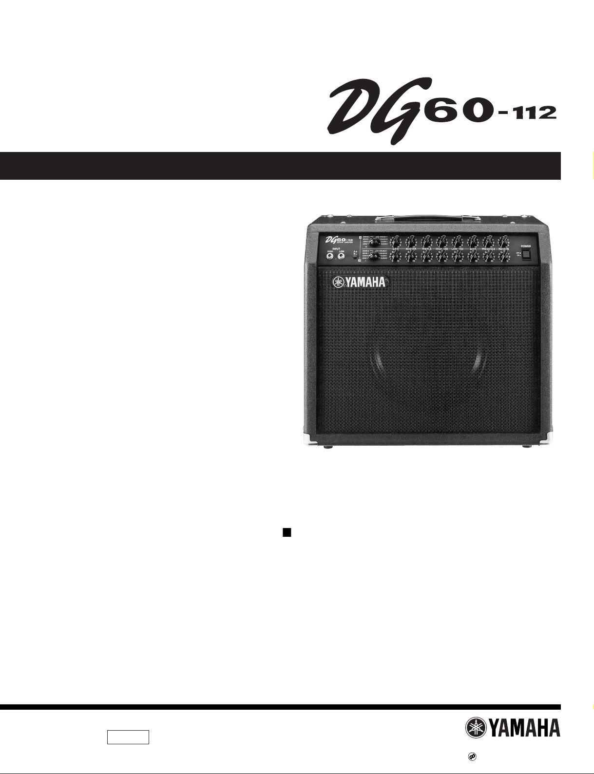
GUITAR AMPLIFIER
CONTENTS
SPECIFICATIONS····································································· 3
PANEL LAYOUT········································································ 4
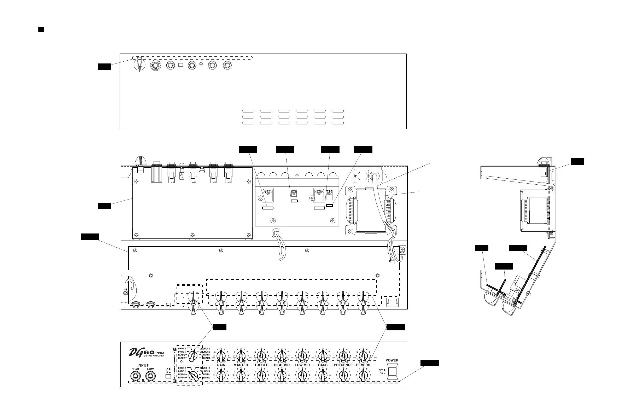
CIRCUIT BOARD LAYOUT······················································· 5
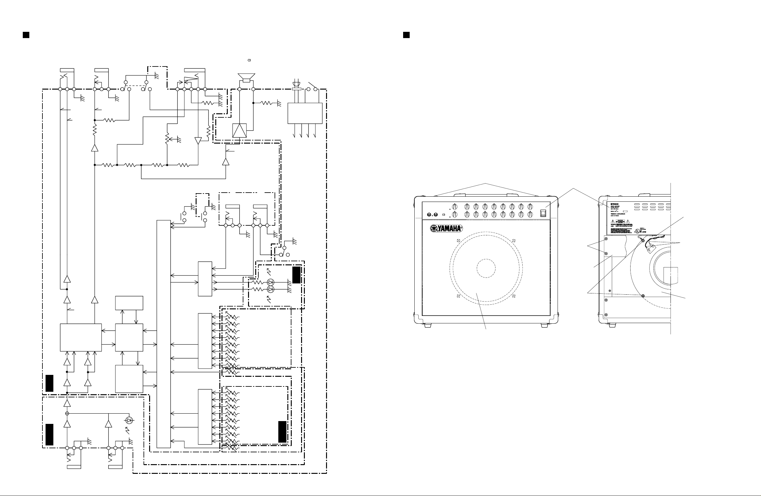
BLOCK DIAGRAM····································································· 6
DISASSEMBLY PROCEDURE·················································· 6
LSI PIN DESCRIPTION····························································· 8
IC BLOCK DIAGRAM ······························································ 10
SELF CHECK AND INSPECTIONS ········································ 12
PARTS LIST
OVERALL CIRCUIT DIAGRAM
CIRCUIT BOARDS

DG60-112
2
WARNING: CHEMICAL CONTENT NOTICE!
The solder used in the production of this product contains LEAD. In addition, other electrical/electronic and/or plastic (where
applicable) components may also contain traces of chemicals found by the California Health and Welfare Agency (and possibly
other entities) to cause cancer and/or birth defects or other reproductive harm.
DO NOT PLACE SOLDER, ELECTRICAL/ELECTRONIC OR PLASTIC COMPONENTS IN YOUR MOUTH FOR ANY REASON
WHAT SO EVER!
Avoid prolonged, unprotected contact between solder and your skin! When soldering, do not inhale solder fumes or expose eyes
to solder/flux vapor!
If you come in contact with solder or components located inside the enclosure of this product, wash your hands before handling
food.
IMPORTANT NOTICE
This manual has been provided for the use of authorized Yamaha Retailers and their service personnel. It has been assumed that
basic service procedures inherent to the industry, and more specifically Yamaha Products, are already known and understood by
the users, and have therefore not been restated.
WARNING: Failure to follow appropriate service and safety procedures when servicing this product may result in personal
injury, destruction of expensive components and failure of the product to perform as specified. For these
reasons, we advise all Yamaha product owners that all service required should be performed by an authorized
Yamaha Retailer or the appointed service representative.
IMPORTANT: This presentation or sale of this manual to any individual or firm does not constitute authorization, certification,
recognition of any applicable technical capabilities, or establish a principal-agent relationship of any form.
The data provided is belived to be accurate and applicable to the unit(s) indicated on the cover. The research engineering, and
service departments of Yamaha are continually striving to improve Yamaha products. Modifications are, therefore, inevitable and
changes in specification are subject to change without notice or obligation to retrofit. Should any discrepancy appear to exist,
please contact the distributor's Service Division.
WARNING: Static discharges can destroy expensive components. Discharge any static electricity your body may have
accumulated by grounding yourself to the ground bus in the unit. (Heavy gauge black wires connect to this
bus.)
IMPORTANT: Turn the unit OFF during disassembly and parts replacement. Recheck all work before you apply power to the
unit.
WARNING
Components having special characteristics are marked and must be replaced with parts having specification equal to those
originally installed.
IMPORTANT NOTICE FOR THE UNITED KINGDOM
Connecting the Plug and Cord
WARNING: THIS APPARATUS MUST BE EARTHED
IMPORTANT. The wires in this main lead are coloured in
accordance with the following code:
GREEN-AND-YELLOW: EARTH
BLUE: NEUTRAL
BROWN: LIVE
As the colours of the wires in the main lead of this apparatus may not
correspond with the coloured markings identifying the terminals in
your plug, proceed as follows:
The GREEN-and-YELLOW wire must be connected to the terminal in
the plug that is marked with the letter E or the safety earth symbol (or
colored GREEN or GREEN-and-YELLOW).
The BLUE wire must be connected to the terminal that is marked with
the letter N (or coloured BLACK).
The BROWN wire must be connected to the terminal that is marked
with the letter L (or coloured RED).
This applies only to products diatributed by Yamaha Kemble Music (U.K.) Ltd.

SPECIFICATIONS
DG60-112
3
Digital Section
Complete Digital Signal Processing
Amplification Type: Internal 8 Channel Preset
Digital Reverb (SPRING)
Speaker Simulator (LINE OUT)
Analog Section
60 W Solid State Power Amp
30 cm Speaker (EMINENCE) x 1
Controller/Switch
Front Panel:GAIN, MASTER, TREBLE, HIGH MID, LOW MID,
BASS, PRESENCE, REVERB, AMP select switch,
for each channel (A/B), Channel select switch (A/B)
Rear Panel: EFFECT BLEND, SP MUTE switch, for each
channel (A/B), EFFECT SEND/RETURN level switch
Indicator
Peak Level Display LED (Red)
Connection Jacks
INPUT HIGH/LOW, EFFECT SEND/RETURN, LINE
OUT/PHONES, FOOT SW (CH SELECT, REVERB):
All Standard Phone Mono Jack
A/D Converter 20 bit + 3 bit floating
D/A Converter 20 bit
Sampling Frequency 48 kHz
Input Level/Impedance
INPUT HIGH: –20 dBm (THRU)/1 MΩ
INPUT LOW: –10 dBm (THRU)/1 MΩ
EFFECT RETURN: 0 dBm/120 kΩ
Output Level/Impedance
SPEAKER: 60 W RMS/8 Ω
LINE OUT: +2 dBm/47 Ω
EFFECT SEND: –2 dBm/1 kΩ
Power Requirements
U.S. and Canadian models : 120 V, 60 Hz
General model : 230 V, 50 Hz
Power Consumption
70 W
Dimensions (W x H x D)
540 x 504 x 276 mm (21.3” x 19.8” x 10.9”)
Weight
18.0 kg (39 lbs 11 oz)
DG60-112
4
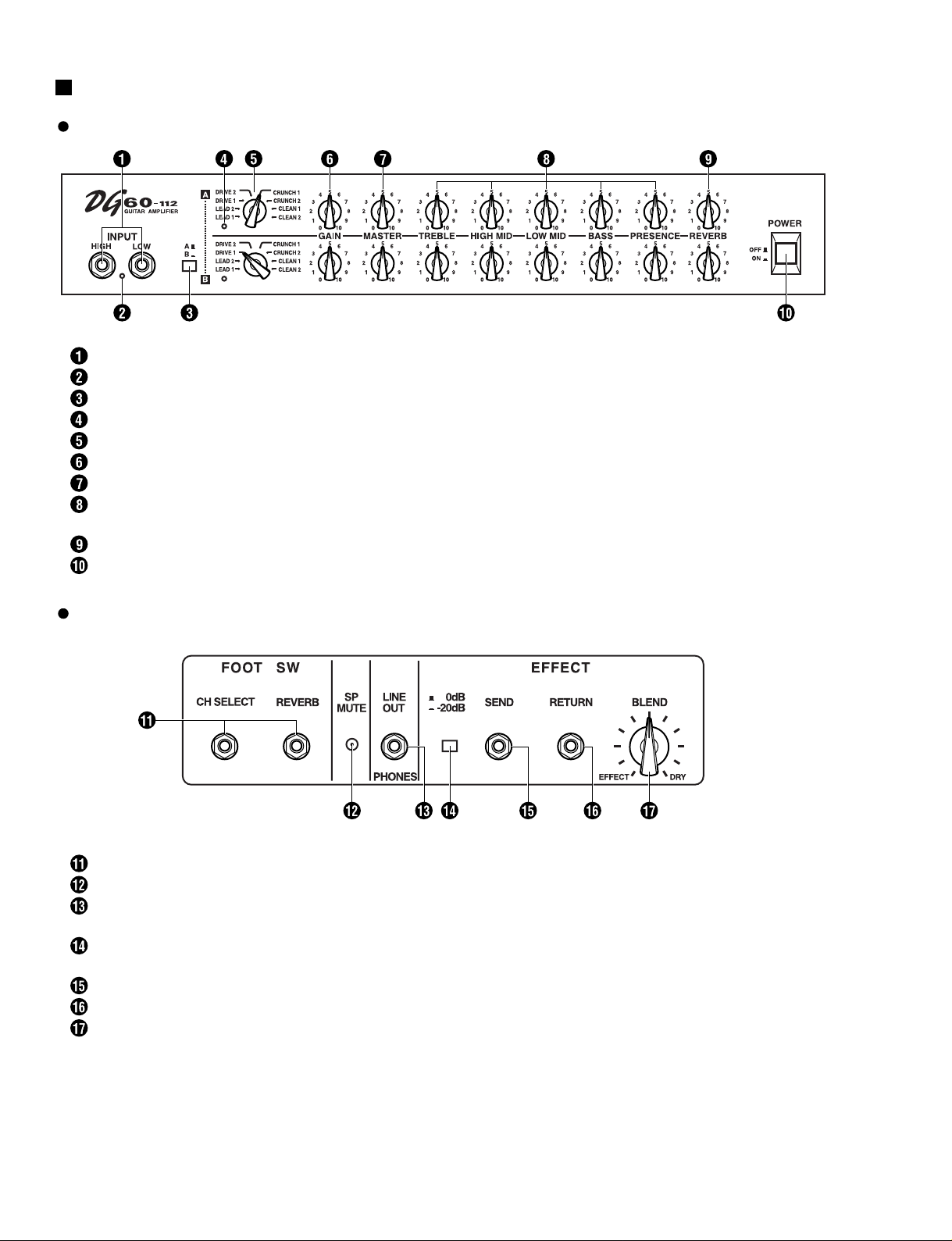
PANEL LAYOUT
Input Jack (INPUT HIGH, LOW)
Peak Indicator
Channel Select Switch
Channel Indicator
Amp Select Switch
Gain Volume (GAIN)
Master Volume (MASTER)
Tone Controls
(TREBLE, HIGH MID, LOW MID, BASS, PRESENCE)
Reverb Volume (REVERB)
Power Switch (POWER)
Foot Switch (FOOT SW)
Speaker Mute Switch (SP MUTE)
Line Out/Head Phone Jack
(LINE OUT/PHONES)
Effect Send/Return Level Switch
(0 dB/-20 dB)
Effect Send Jack (EFFECT SEND)
Effect Return Jack (RETURN)
Blend Knob (BLEND)
Front Panel
Rear Panel
DM
DM
SW
SW
DM
MAIN
(Bottom)
(Top)
1/5
MAIN 1/5
MAIN 1/5
MAIN 2/5 MAIN 3/5 MAIN 4/5 MAIN 5/5
A-CH
A-CH
Power transformer
AC cord
• Top view
• Front view
• Rear view
• Side view
DG60-112
5
CIRCUIT BOARD LAYOUT
DM
SW
MAIN
INPUT
HIGH
INPUT
LOW
PEAK
ACH BCH
IC201
JK202
JK201
IC202 IC1
IC2
97
IC201
LD201
84 81
3
12
AMP SELECT (SW401)
GAIN (VR302)
MASTER (VR303)
TREBLE (VR304)
HIGH MID (VR305)
LOW MID (VR306)
BASS (VR307)
PRESENCE (VR308)
REVERB (VR309)
AMP SELECT (SW402)
GAIN (VR202)
MASTER (VR203)
TREBLE (VR204)
HIGH MID (VR205)
LOW MID (VR206)
BASS (VR207)
PRESENCE (VR208)
REVERB (VR209)
14 15 11 1 5 2 4
12 14 15 11 1 5 2 4
13
80 85 83
313
82
31
47 21
21
67 31
526 7
5727
MUTE
IC4
MUTE MUTE
MUTE
BLEND
IC6
VR1
75
IC6
JK4
SW3
SW2
98
TEST
SP MUTE
BUF
(IC21)
9795,966,7
9,122,5
47
11 14
JK5
SW202
BCH
LD402LD401
ACH
31
EFECT DRY
MUTE
CH SELECT A/B
REVERB ON/OFF
+B/-B
+15V/-15V
+5V
MUTE
IC5
31
IC5
3
+R-RA/D
-L
R
D/A
L
+L
4
67
4
5
6
AK4520A-VF-E2
ADC/DAC
DSP3
YSS228E-F
(IC14)
MPX
(IC19)
MPX
(IC20)
CPU HD6473042FP16
(IC17)
DSP2
YSS228E-F
(IC15)
DRAM
4M
(IC16)
(IC3)
LINE
OUT/HEAD
PHONES
SEND
PUSH SW.
RETURN
SP '12
8
AC
POWER
SW
0/-20 dBm
JK3
JK2
SW1
JK1
BT202
D201,202
POWER
AMP
BT203
SW201
PUSH SW.
CH A/B
KEC-54180
POWER
SUPPLY
A-CH
BLOCK DIAGRAM DISASSEMBLY PROCEDURE
DG60-112
6
[30]: Oval Head Screw 5.0X35 MFC2BL (VP104600)
[60]: Hexagonal Nut 4.0 MFZN2Y (03760900)
[70]: Oval Head Yapping Screw-1 4.0X30 MFC2BL (EN240090)
(Fig. 1)
[70]
[120]
[30]
[60]
Pre-main unit
Back board (U)
Speaker
Speaker wire
Speaker
1. Pre-Main Unit
1-1 Remove the four (4) screws marked [70]. The back board
(U) can then be removed. (Fig. 1)
1-2 Remove the speaker wires and the screw marked [120].
(Fig. 1)
1-3 Remove the four (4) screws marked [30]. The pre-main
unit can then be removed by sliding it backward. (Fig. 1)
2. Speaker
2-1 Remove the four (4) screws marked [70]. The back board
(U) can then be removed. (Fig. 1)
2-2 Remove the four (4) hexagonal nuts marked [60]. The
speaker can then be removed. (Fig. 1)
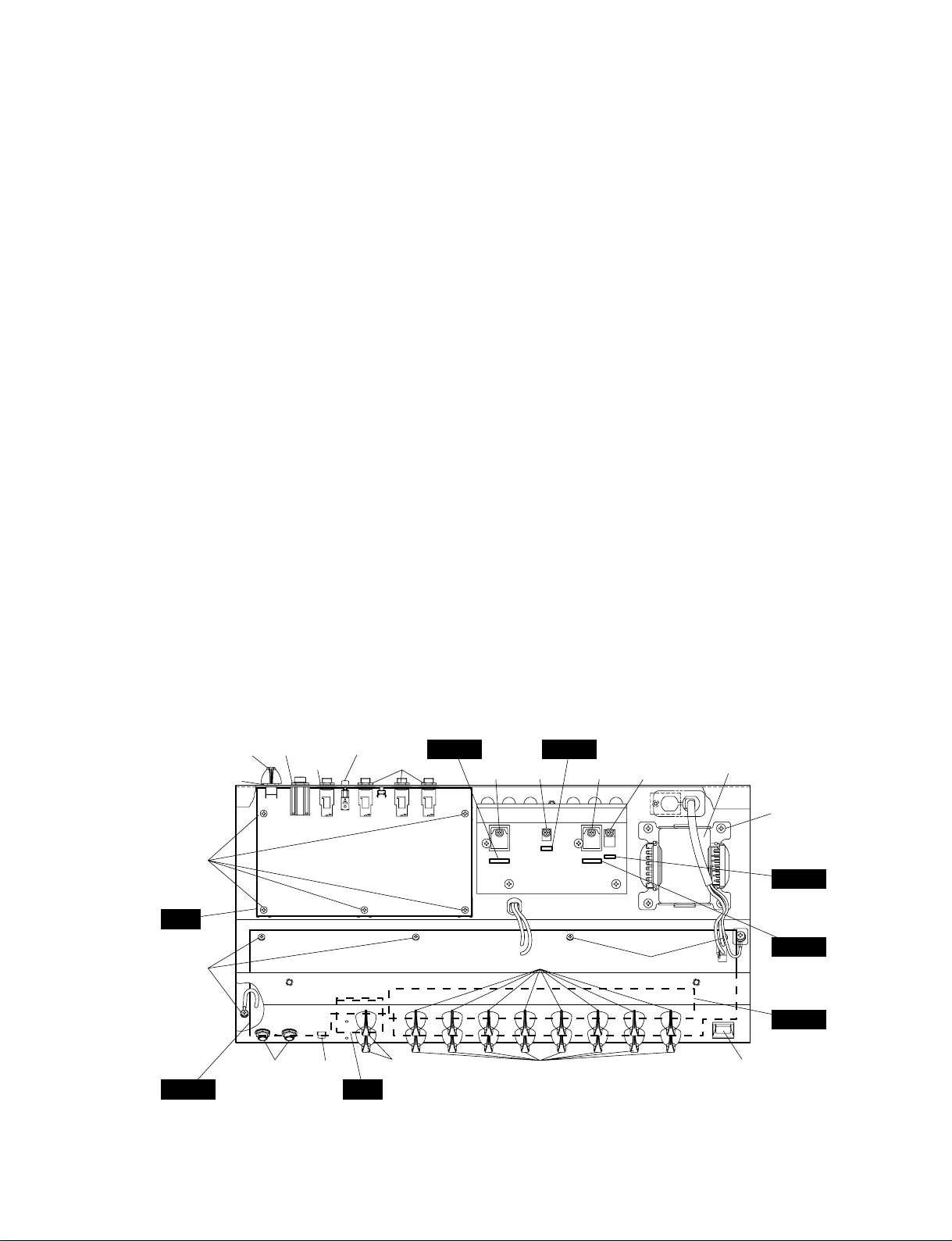
3. DM Circuit Board
3-1 Remove the pre-main unit. (See Procedure 1.)
3-2 Remove the BLEND knob marked [90A], the four (4)
hexagonal nuts marked [130A], the hexagonal nut marked
[190] and the hexagonal nut marked [210].
3-3 Remove the five (5) screws marked [80A]. The DM
circuit board can then be removed. (Fig. 2)
3-4 Remove the button marked [100A] form the DM circuit
board. (Fig. 2)
SW
2/5 3/5
Power transformer
[80]: Bind Head Tapping Screw-B 3.0X8 MFZN2BL (EP600190)
[130]: Hexagonal Nut 9.0 12X2 MFNI33 (LX200060)
[190]: Hexagonal Nut 12.0 14X2 MFC2BL (VD794100)
[210]: Hexagonal Nut 9.0 11X2 MFZN2BL (VJ388000)
[270]: Bind Head Tapping Screw-C A4.0X8 MFZN2BL (VC688900)
[290]: Bind Head Screw SP 3.0X12 MFZN2Y (VB763800)
(Fig. 2)
[210]
[80A]
[90A]
[130A] [130A]
[290A]
[100A][190]
[290B] [290C] [290D]
[270]X4
[80B]
[90C], [B]
MAIN MAIN
MAIN 5/5
MAIN 4/5
[90B], [A][90D], [A][100B] [110][130B]
[80B]
DM
MAIN 1/5
A-CH
DG60-112
7
4. MAIN (1/5-5/5), A-CH and SW Circuit
Boards
4-1 Remove the pre-main unit. (See Procedure 1.)
4-2 Each circuit board can then be removed in its manner as
below. (Fig. 2)
MAIN 1/5 Circuit Board
Remove the eight (8) knobs marked [90B], the eight (8)
hexagonal nuts marked [A], the two (2) hexagonal nuts
marked [130B] and the five (5) screws marked [80B].
Remove the knob marked [100B] and the knob marked [110]
from the MAIN 1/5 circuit board. (Fig. 2)
MAIN 2/5 Circuit Board
Remove the screw marked [290A]. (Fig. 2)
MAIN 3/5 Circuit Board
Remove the screw marked [290B]. (Fig. 2)
MAIN 4/5 Circuit Board
Remove the screw marked [290C]. (Fig. 2)
MAIN 5/5 Circuit Board
Remove the screw marked [290D]. (Fig. 2)
A-CH Circuit Board
Remove the eight (8) knobs marked [90C] and the eight
(8) hexagonal nuts marked [B]. (Fig. 2)
SW Circuit Board
Remove the two (2) knobs marked [90D] and the two
(2) hexagonal nuts marked [C]. (Fig. 2)
5. Power Transformer
5-1 Remove the pre-main unit. (See Procedure 1.)
5-2 Remove the four (4) screws marked [270]. The power
transformer can then be removed. (Fig. 2)
DG60-112
8
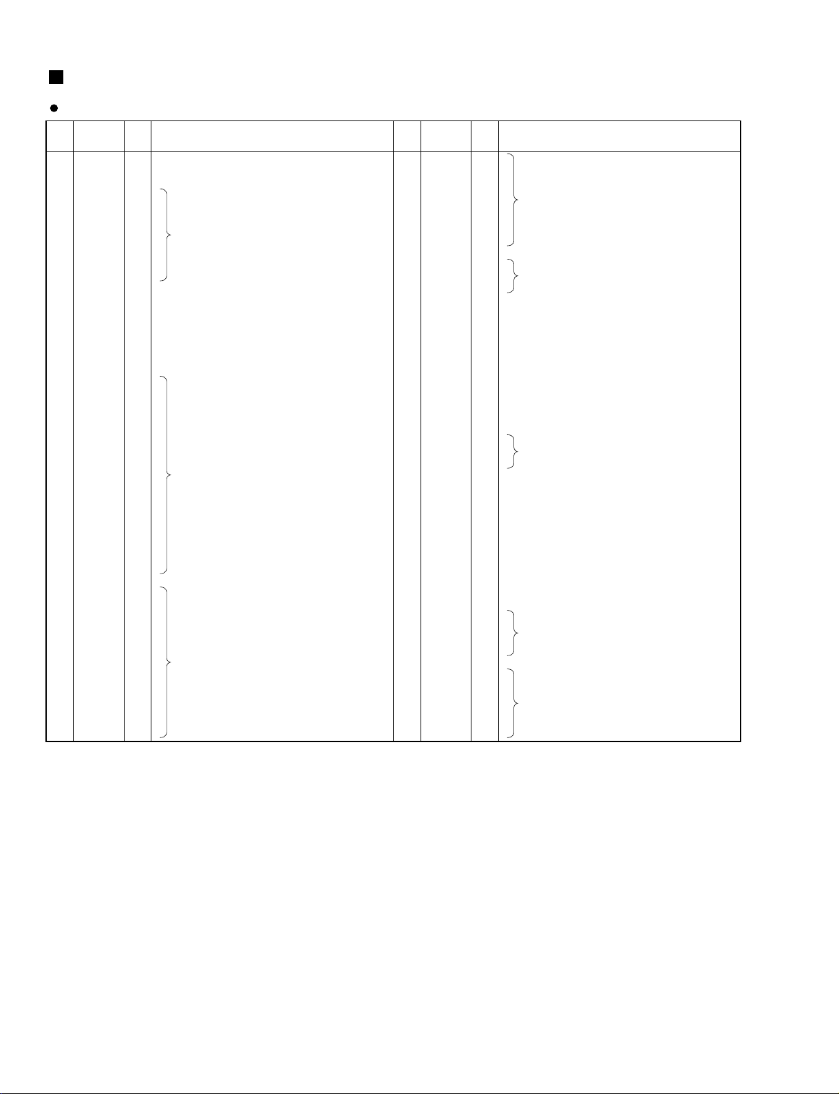
LSI PIN DESCRIPTION
PIN
NO.
I/O FUNCTIONNAME
PIN
NO.
I/O FUNCTIONNAME
1
2
3
4
5
6
7
8
9
10
11
12
13
14
15
16
17
18
19
20
21
22
23
24
25
26
27
28
29
30
31
32
33
34
35
36
37
38
39
40
41
42
43
44
45
46
47
48
49
50
PA6
PA7
VCC
PB0
PB1
PB2
PB3
PB4
PB5
PB6//DREQ0
PB7//DREQ1
/RESO
VSS
P90/TXD0
P91/TXD1
P92/RXD0
P93/RXD1
P94/SCK0
P95/SCK1
P40/D0
P41/D1
P42/D2
P43/D3
VSS
P44/D4
P45/D5
P46/D6
P47/D7
D8
D9
D10
D11
D12
D13
D14
D15
VCC
A0
A1
A2
A3
A4
A5
A6
A7
VSS
A8
A9
A10
A11
O
O
I
I
I
I
I
I
I
I
O
O
O
I
I
O
I
I/O
I/O
I/O
I/O
I/O
I/O
I/O
I/O
I/O
I/O
I/O
I/O
I/O
I/O
I/O
I/O
O
O
O
O
O
O
O
O
O
O
O
O
Port A
Address bus
Power supply
Port B
Reset
Ground
Transmit data (MIDI OUT)
KSN-ACK
Receive data (MIDI IN)
KSN-RX
Port 9
Port 9
(Ground)
Data bus
Power supply
Address bus
(Ground)
51
52
53
54
55
56
57
58
59
60
61
62
63
64
65
66
67
68
69
70
71
72
73
74
75
76
77
78
79
80
81
82
83
84
85
86
87
88
89
90
91
92
93
94
95
96
97
98
99
100
A12
A13
A14
A15
A16
A17
A18
A19
VSS
P60//WAIT
P61//BREQ
P62//BACK
Ø
/STBY
/RES
NMI
VSS
EXTAL
XTAL
VCC
/AS
/RD
/HWR
/LWR
MD0
MD1
MD2
AVCC
VREF
P70/AN0
P71/AN1
P72/AN2
P73/AN3
P74/AN4
P75/AN5
P76/AN6
P77/AN7
AVSS
P80
P81//CS3
P82//CS2
P83//CS1
P84//CS0
VSS
PA0
PA1
PA2
PA3
PA4
PA5
O
O
O
O
O
O
O
O
I
I
I
O
I
I
I
I
O
O
O
O
O
I
I
I
I
I
I
I
I
I
I
I
I
O
O
O
O
O
I
I
I
O
O
O
Address bus
Ground
Port 6
Ø out
Stand-by mode signal
Reset
Non-maskable interrupt
Ground
Clock
Clock
Power supply
Address strobe
Read strobe
Write strobe (High)
Write strobe (Low)
Mode select
Analog power supply
Reference voltage
Analog data input (EQ)
Analog input (EQ)
Analog data input
Analog input (CS)
Analog data input (BEND)
Analog input (MOD)
Analog input (FC)
Analog input (BAT)
Analog ground
Port 8
Chip select
Ground
Port A
HD6433042SC10FP (XW325100) CPU
DM: IC17
PIN
NO.
I/O FUNCTIONNAME
PIN
NO.
I/O FUNCTIONNAME
1
2
3
4
5
6
7
8
9
10
11
12
13
14
15
16
17
18
19
20
21
22
23
24
25
26
27
28
29
30
31
32
33
34
35
36
37
38
39
40
41
42
43
44
45
46
47
48
49
50
51
52
53
54
55
56
57
58
59
60
61
62
63
64
65
66
67
68
69
70
71
72
73
74
75
76
77
78
79
80
VSS
XI
XO
VDD
/SYNCI
/SYNCO
CKI
CKO
CKSL
VSS
MCKS
/SSYNC
/IC
/TEST
BTYP
/IRQ
TRIG
VDD
VSS
/CS
/DS
R/W
CA7
CA6
CA5
CA4
CA3
CA2
CA1
CA0/CD15
CD14
CD13
CD12
CD11
CD10
CD09
CD08
CD07
CD06
VSS
VDD
CD05
CD04
CD03
CD02
CD01
CD00
/DTACK
SI0
SI1
SI2
SI3
SI4
SI5
SI6
SI7
VSS
VDD
SO0
SO1
SO2
SO3
SO4
SO5
SO6
SO7
DB00
DB01
DB02
DB03
DB04
DB05
DB06
DB07
DB08
DB09
DB10
DB11
DB12
VDD
I
I
O
I
O
I
I
I
I
I
I
O
I/O
I
I
I
I
I
I
I
I
I
I
I/O
I/O
I/O
I/O
I/O
I/O
I/O
I/O
I/O
I/O
I/O
I/O
I/O
I/O
I/O
I/O
O
I
I
I
I
I
I
I
I
O
O
O
O
O
O
O
O
I/O
I/O
I/O
I/O
I/O
I/O
I/O
I/O
I/O
I/O
I/O
I/O
I/O
Ground
System master clock input (60 M or30 MHz)
System master clock input (60 M or30 MHz)
Power supply
System synch. input
System synch. output
System clock input (30 MHz)
System clock output (30 MHz)
System master clock select (0:60 M,1:30 MHz)
Ground
Master clock for serial I/O(128 xFs)
Synch. signal for serial I/O
Initial clear
Test mode setting
CPU data bus 8/16 bit select(0:8,1:16)
Interrupt request
Trigger signal
Power supply
Ground
Chip select
Data strobe
Read/Write select
CPU address bus
CPU address/data bus
CPU data bus
Ground
Power supply
CPU data bus
DTACK signal output
Serial data input
Ground
Power supply
Serial data output
Parallel data bus
Power supply
81
82
83
84
85
86
87
88
89
90
91
92
93
94
95
96
97
98
99
100
101
102
103
104
105
106
107
108
109
110
111
112
113
114
115
116
117
118
119
120
121
122
123
124
125
126
127
128
129
130
131
132
133
134
135
136
137
138
139
140
141
142
143
144
145
146
147
148
149
150
151
152
153
154
155
156
157
158
159
160
VSS
DB13
DB14
DB15
DB16
DB17
DB18
DB19
DB20
DB21
DB22
DB23
DB24
DB25
DB26
DB27
DB28
DB29
DB30
DB31
TIMO/DBOE
VSS
VDD
DA00
DA01
DA02
DA03
DA04
DA05
DA06
DA07
DA08
DA09
DA10
DA11
DA12
DA13
DA14
DA15
VSS
VDD
DA16
DA17
DA18
DA19
DA20
DA21
DA22
DA23
DA24
DA25
DA26
DA27
DA28
DA29
DA30
DA31
VDD
VSS
A00
A01
A02
A03
A04
A05
A06
A07
A08
A09
A10
A11
A12
A13
A14
A15/RAS
A16/CAS
A17/CE
/WE
/OE
VDD
I/O
I/O
I/O
I/O
I/O
I/O
I/O
I/O
I/O
I/O
I/O
I/O
I/O
I/O
I/O
I/O
I/O
I/O
I/O
I/O
I/O
I/O
I/O
I/O
I/O
I/O
I/O
I/O
I/O
I/O
I/O
I/O
I/O
I/O
I/O
I/O
I/O
I/O
I/O
I/O
I/O
I/O
I/O
I/O
I/O
I/O
I/O
I/O
I/O
I/O
I/O
I/O
I/O
O
O
O
O
O
O
O
O
O
O
O
O
O
O
O
O
O
O
O
O
Ground
Parallel data bus
Timing signal/Parallel data bus control
Ground
Power supply
External memory data bus
Ground
Power supply
External memory data bus
Power supply
Ground
External memory address bus
External memory address bus/Row address strobe
External memory address bus/Column address strobe
External memory address bus/Chip enable
External memory write enable
External memory output enable
Power supply
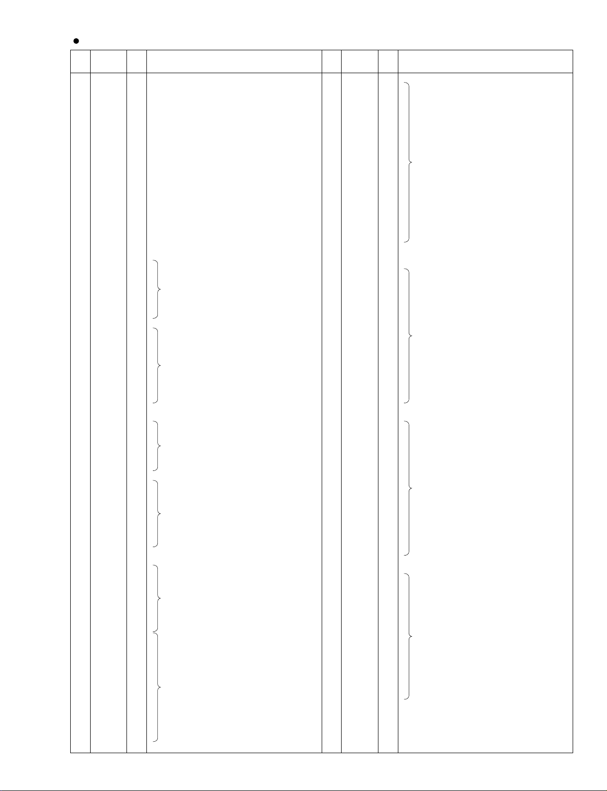
YSS228E-F (XQ962D00) DSP3 (Digital Signal Processor)
DM: IC14, 15
DG60-112
9
 Loading...