

Yaesu FT-857 Service Manual
Technical Supplement
©2003 VERTEX STANDARD CO., LTD. EH007M90A
VERTEX STANDARD CO., LTD.
4-8-8 Nakameguro, Meguro-Ku, Tokyo 153-8644, Japan
VERTEX STANDARD
US Headquarters
10900 Walker Street, Cypress, CA 90630, U.S.A.
International Division
8350 N.W. 52nd Terrace, Suite 201, Miami, FL 33166, U.S.A.
YAESU EUROPE B.V.
P.O. Box 75525, 1118 ZN Schiphol, The Netherlands
YAESU UK LTD.
Unit 12, Sun Valley Business Park, Winnall Close
Winchester, Hampshire, SO23 0LB, U.K.
VERTEX STANDARD HK LTD.
Unit 5, 20/F., Seaview Centre, 139-141 Hoi Bun Road,
Kwun Tong, Kowloon, Hong Kong
Introduction
This manual provides technical information necessary for servicing the FT-857 HF/VHF/UHF Ultra-Compact Transceiver.
Servicing this equipment requires expertise in handling surface-mount chip components. Attempts by non-qualified per-
sons to service this equipment may result in permanent damage not covered by the warranty, and may be illegal in some
countries.
Two PCB layout diagrams are provided for each double-sided circuit board in the Transceiver. Each side of is referred to
by the type of the majority of components installed on that side (“leaded” or “chip-only”). In most cases one side has only
chip components, and the other has either a mixture of both chip and leaded components (trimmers, coils, electrolytic
capacitors, ICs, etc.), or leaded components only.
While we believe the technical information in this manual to be correct, VERTEX STANDARD assumes no liability for
damage that may occur as a result of typographical or other errors that may be present. Your cooperation in pointing out
any inconsistencies in the technical information would be appreciated.
Contents
Specifications .................................................. 2
Exploded View & Miscellaneous Parts ...... 5
Connection Diagram ...................................... 7
Block Diagram................................................. 8
Circuit Description ........................................ 9
Alignment ...................................................... 12
Board Unit (
MAIN Unit ................................................................ 23
PLL Unit..................................................................... 49
PA Unit ...................................................................... 55
PANEL Unit .............................................................. 67
REF Unit..................................................................... 73
PHONE-JACK Unit .................................................. 74
VR Unit ...................................................................... 75
CONNECTOR Unit .................................................. 76
DSP-2 Unit (Option) ................................................. 77
TCXO-9 Unit (Option).............................................. 80
Schematics, Layouts & Parts
)
1

Specifications
General
Frequency Range: Receive: 0.1-56 MHz, 76-108 MHz, 118-164 MHz, 420-470 MHz
Transmit: 160 - 6 Meters, 2 Meters, 70 Centimeters (Amateur bands only)
Emission Modes: A1 (CW), A3 (AM), A3J (LSB/USB), F3 (FM),
F1 (9600 bps packet), F2 (1200 bps packet)
Synthesizer Steps (Min.): 10 Hz (CW/SSB), 100 Hz (AM/FM/WFM)
Antenna Impedance: 50 Ohms, Unbalanced
Operating Temp. Range: 14 ºF to 140 ºF (–10 °C to +60 °C)
Frequency Stability: ±4 ppm from 1 min. to 60 min after power on. @25 °C: 1 ppm/hour
±0.5 ppm/1 hour @25 °C, after warmup (with optional TCXO-9)
Supply Voltage: Normal: 13.8 VDC ±15 %, Negative Ground
Current Consumption: Squelched: 550 mA (Approx.)
Receive: 1 A
Transmit: 22 A
Case Size (W x H x D): 6.1” x 2.0” x 9.2” (155 x 52 x 233 mm)
Weight (Approx.): 4.6 lb. (2.1 kg)
Transmitter
RF Power Output: SSB/CW/FM AM Carrier
(@13.8 V DC) 160- 6 M: 100 W 25 W
2 M: 50 W 12.5 W
70 CM: 20 W 5 W
Modulation Types: SSB: Balanced Modulator,
AM: Early Stage (Low Level),
FM: Variable Reactance
FM Maximum Deviation: ±5 kHz (FM-N: ±2.5 kHz)
Spurious Radiation: –50 dB (1.8-29.7 MHz)
–60 dB (50/144/430 MHz)
Carrier Suppression: >40 dB
Opp. Sideband Suppression: >50 dB
SSB Frequency Response: 400 Hz-2600 Hz (–6 dB)
Microphone Impedance: 200-10k Ohms (Nominal: 600 Ohms)
2

Receiver
Circuit Type: Double-Conversion Superheterodyne (SSB/CW/AM/FM)
Superheterodyne (WFM)
Intermediate Frequencies: 1st: 68.33 MHz (SSB/CW/AM/FM); 10.7 MHz (WFM)
2nd: 455 kHz
Sensitivity: SSB/CW AM FM
100 kHz-1.8 MHz – 32 µV –
1.8 MHz-28 MHz 0.2 µV 2 µV –
28 MHz-30 MHz 0.2 µV 2 µV 0.5 µV
50 MHz-54 MHz 0.125 µV 1 µV 0.2 µV
144/430 MHz 0.125 µV – 0.2 µV
(SSB/CW/AM = 10 dB S/N, FM = 12 dB SINAD)
Squelch Sensitivity: SSB/CW/AM FM
100 kHz-1.8 MHz – –
1.8 MHz-28 MHz 2.5 µV –
28 MHz-30 MHz 2.5 µV 0.32 µV
50 MHz-54 MHz 1 µV 0.16 µV
144/430 MHz 0.5 µV 0.16 µV
Image Rejection: HF/50 MHz: 70 dB,
144/430 MHz: 60 dB
IF Rejection: 60 dB
Selectivity (–6/–60 dB): SSB/CW: 2.2 kHz/4.5 kHz
AM: 6 kHz/20 kHz
FM: 15 kHz/30 kHz
FM-N: 9 kHz/25 kHz
SSB (optional YF-122S installed): 2.3 kHz/4.7 kHz (–66 dB)
CW (option YF-122C installed): 500 Hz/2.0 kHz
CW (option YF-122CN installed): 300 Hz/1.0 kHz
AF Output: 2.5 W (@4 Ohms, 10% THD or less)
AF Output Impedance: 4-16 Ohms
Specifications
Specifications are subject to change without notice, and are guaranteed within the amateur bands only.
3

Note
4
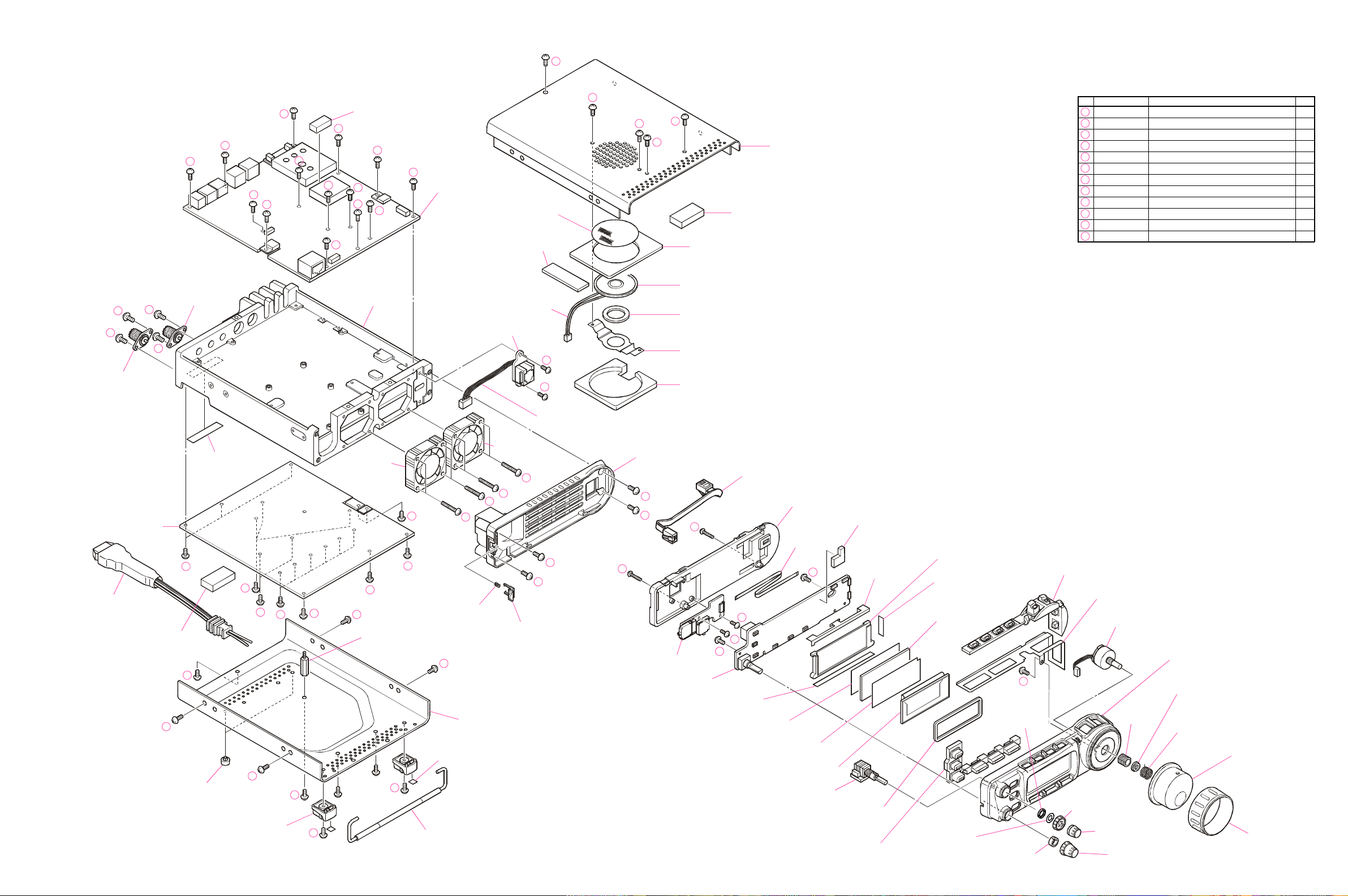
Exploded View & Miscellaneous Parts
11
Non-designated parts are available only as part of a designated assembly.
10
10
P1090352 (TYPE "M")
P1090547 (TYPE "N")
CONNECTOR
PA UNIT
T9207026
WIRE ASSY
PACKING SHEET (GAP)
7
P1090352
CONNECTOR
10
10
RA0484500
SHEET (ANT)
7
RA0446300
11
11
S4000045
CASE LEG (x2 pcs)
7
7
8
7
7
11
RA0469800
LEG (A) (x2 pcs)
11
11
11
11
RA0459600
TOP CASE
RA0453200
GASCKET (SHIELD)
RA0398100
SPONGE RUBBER (SP)
7
7
RA0471400
SPONGE (B)
8
2
7
2
7
MAIN UNIT
RA0257600
SP NET
7
7
RA0489500
7
SPONGE RUBBER (DSP)
Ref.
VXSTD P/N Description Qty
1
U00315007 PAN HEAD SCREW M3X15B 4
2
U02208002 PAN HEAD SCREW SM2.6X8NI 2
3
U02306002 SEMS SCREW SM3X6NI 6
4
U20304007 BINDING HEAD SCREW M3X4B 2
5
U24104001 TAPTITE SCREW M2X4 2
6
U24105001 TAPTITE SCREW M2X5 3
7
U24205001 TAPTITE SCREW M2.6X5 21
8
U24206003 TAPTITE SCREW M2.6X6NIB 4
9
U24210007 TAPTITE SCREW M2.6X10B 4
10
U24306002 TAPTITE SCREW M3X6NI 4
11
U31205007 OVAL HEAD SCREW M2.6X5B 13
12
U43110007 TAPTITE SCREW M2X10B 2
M40900150
RA0428700
CHASSIS
T9207004
WIRE ASSY
SPEAKER
RA0283900
SPONGE RUBBER (SP-B)
CONNECTOR UNIT
RA0413400
6
6
SP HOLDER
RA0483900
SPONGE RUBBER (SP-C)
T9207023
WIRE ASSY
M2090036
M2090036
FAN
FAN
1
1
1
8
1
RA0450600
SUB PANEL
9
9
T9101530
CT CABLE
RA0450500
REAR PANEL
12
T9207024
RA0489800
SPONGE RUBBER (TX)
WIRE ASSY
RA0450900
7
7
7
3
11
S5000240
SPACER
R0137551
COIL SPRING
11
R0450700
RELEASE KNOB
9
9
12
5
5
6
6
PHONE-JACK UNIT
RA0481000
SHEET (LCD)
LCD HOLDER
RA0485400
LIGHT SHEET (B)
RA0451000
LIGHT GUIDE (LCD)
PANEL UNIT
RA0485300
RA0459700
BOTTOM CASE
RA0484100
SPONGE RUBBER (LEG) (x2 pcs)
LIGHT SHEET (A)
RA0452400
REFLECTOR SHEET
RA0452500
DIFFUSER SHEET
Q7000428
RA0111400
RING NUT
RA0451100
KNOB ASSY (MODE)
6
RA0450800
HOLDER (MODE)
Q9000796
ROTARY ENCODER
R6144801
NUT
RA0450200
FRONT PANEL ASSY
R3135000A
WASHER
R0136380
COIL SPRING
RA0452000
KNOB MAIN ASSY
LCD MODULE
11
4
4
RA0471900
STAND (S)
VR UNIT
RA048210B
SPONGE RUBBER (WND)
RA0451900
KNOB ASSY (FUNC)
RA0473600
WASHER (KNOB)
SPACER KNOB (SEL)
RA0473600
RA0269500
ROTARY KNOB (SQL)
RA0269400
ROTARY KNOB (AF)
RA0269600
ROTARY KNOB (SEL)
RA0452300
RUBBER RING
5

Note
6
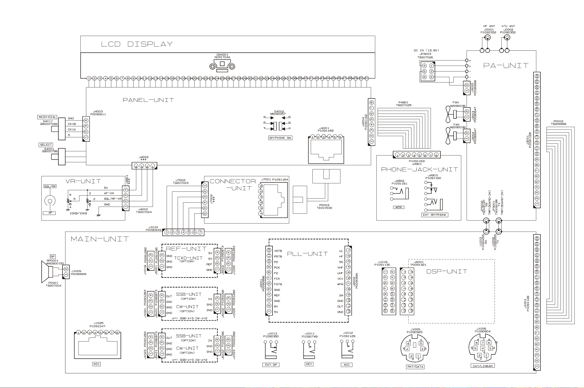
Connection Diagram
7
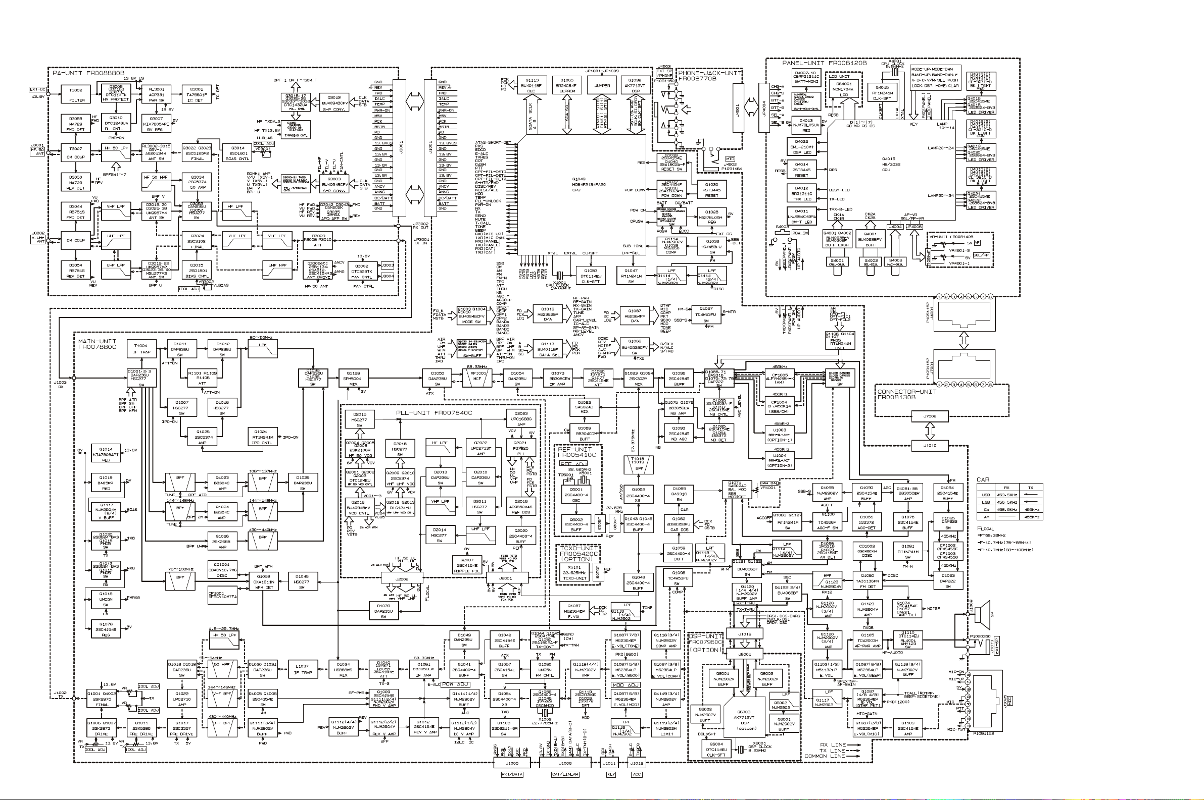
Block Diagram
8

Circuit Description
Receive Signal Circuitry
RF Stages
Signals between 0.1 and 56 MHz received at the antenna
terminal pass through a low-pass filter, selected according to the receiving frequency, then pass to another lowpass filter, to remove unwanted out-of-band signals. The
filtered receiving signal passes, through one of the following circuits, to the 1st Mixer Q1128 (SPM5001): (1)
an attenuator network (–10dB) which consists of resistors R1101, R1108, R1109; (2) a “through” circuit enabled
via diodes D1011 and D1012 (both DAP236U); or (3)
RF amplifier Q1025 (2SC5374).
Received 430 MHz signals, after passing through a highpass filter composed of L3058, L3069, C3250, C3251,
C3253, C3258, and C3298, are passed through low-pass
filter composed of L3043, L3044, C3209, C3211, C3214,
C3215, C3246, and C3255, and through a directional coupler, to the UHF T/R switch circuit composed of diode
switch D3019/D3022 (both UM9957F), D3023 , and
D3039 (both HSU277). Then the signals are fed to the
1st Mixer Q1128 via the RF-AMP Q1026 (2SK2685).
Received 145 MHz signals, after passing through a highpass filter composed of L3055, L3056, L3067, C3248,
C3249, C3252, and C3254, are passed through a low-pass
filter composed of L3040, L3041, C3204, C3205, C3210,
C3213, and C3216, and a directional coupler, to the VHF
T/R switch circuit, composed of diode switch D3018/
D3021 (both UM9957F). Then the signals are fed to 1st
Mixer Q1128 via the RF-AMP, Q1024 (BB304CDW).
Received 76-108 MHz signals, after passing through a
high-pass filter composed of L3055, L3056, L3067,
C3248, C3249, C3252, and C3254, are passed through
low-pass filter composed of L3040, L3041, C3204, C3205,
C3210, C3213, and C3216, and a directional coupler, to
the T/R switch circuit, composed of diode switch D3018/
D3021 (both UM9957F). Then it is fed to the Wide-FM
IF IC Q1058 (CXA1611N) on the MAIN Unit.
1st Mixer Circuit/1st IF Circuit
The 1st mixer on the MAIN Unit consists of quad MOS
FET Q1128 (SPN5001), where the receiving signal is
mixed with the 1st local signal (68.430-538.330 MHz) from
the PLL Unit. The resulting output signal (68.33 MHz)
passes through monolithic crystal filter (MCF) XF1001
(MF68Q, BW: ±6.0 kHz) to obtain the 1st IF signalwith a
center frequency of 68.33 MHz. The IF signal passes
through the 1st IF amplifier Q1073 (BB305CEW) to the
2nd Mixer, Q1083 and Q1084 (both 2SK302Y).
2nd Mixer Circuit/2nd IF Circuit
The 2nd Mixer consists of FETs Q1083 and Q1084 (both
2SK302Y) on the MAIN Unit, where the 1st IF signal is
mixed with the 2nd local signal (67.875 MHz). The resulting output signal (455 kHz) is applied to the 2nd IF
filter which is matched to the receiving mode: either
CF1004, CF1005 or an optional mechanical filter.
Noise Blanker Circuit
A portion of the 2nd IF signal is amplified by Noise
Blanker Amplifiers Q1075 and Q1079 (both
BB305CEW) on the MAIN Unit, and then rectified by
D1064 (1SS372). This output is applied to the Noise
Blanker Controllers, Q1093 (2SC4154E) and Q1099
(2SA1602A), which a yield Blanking signal according
to the timing of the incoming noise pulses. Then Blanking signal controls the Noise Blanker Gate D1066
(BAS316), to slice out the impulse noise from the signal.
AGC Circuit
The AGC circuit consists of D1061 (1SS372), transistor
Q1090 (2SC4154E), and associated parts on the MAIN
Unit. Output from the AGC circuit is fed back to the IF
AGC circuit that controls the gain of the IF amplifier FETs.
FM IF Circuit/FM Demodulator Circuit
On FM, the 2nd IF signal passes through the buffer amplifier Q1094 (2SC4154E) and 2nd IF filters (CF1002
and CF1003) to the FM IF IC Q1080 (TA31135FN) which
contains a mixer, limiter amplifier, filter amplifier, squelch
trigger, and demodulator. The demodulated audio signal
at Q1080 passes through a low-pass filter (R1339 and
C1282) and a de-emphasis circuit (R1303 and C1345),
then proceeds to the Audio Amplifier Circuit.
The squelch circuit selectively amplifies the noise component of the demodulator output using the filter amplifier inside the FM IF IC and an active band-pass filter
consisting of an externally attached resistor and capacitor. Signal detection is performed by D1057 (DA221).
SSB/CW Demodulator Circuit
The 2nd IF SSB/CW signal passes through buffer amplifiers Q1088 and Q1081 (both BB305CEW) to the SSB
balanced demodulator Q1071 (SA602AD) which produces audio by applying the carrier signal from the CARDDS IC Q1062 (AD9835BRU). The demodulated audio
signal is stripped of high-frequency components by an
active low-pass filter, op-amp IC Q1120 (NJM2902V),
then is applied to the Audio Amplifier Circuit.
AM Demodulator Circuit
The 2nd IF AM signal passes through buffer amplifiers
Q1088 and Q1081 (both BB305CEW) to the AM demodu-
lator D1055 (BAS316), yielding demodulated audio signal which is applied to the Audio Amplifier Circuit.
Audio Amplifier Circuit
The demodulated audio signal is passed through AF preamplifier Q1119 (NJM2902V) and electronic volume control IC Q1087 (M62364EP) to the AF Amplifier IC Q1105
(TDA2003H) which drives the internal or external speaker
to a maximum output of approximately 2.5 Watts.
9

Circuit Description
Transmit Signal Circuitry
Microphone Amplifier Circuit
The audio signal from microphone jack is amplified by
audio amplifier Q1109 (2SC4154E) on the MAIN Unit,
and then is applied to electronic volume control IC Q1087
(M62364EP), the level of which is set via the User Menu.
SSB Modulator Circuit
The output (audio signal) from the electronic volume control IC is passed through audio amplifier Q1118
(NJM2902V) to the balanced modulator IC Q1071
(SA602AD) which produces a Double Sideband (DSB)
signal by applying the carrier signal from the CAR-DDS
IC Q1062 (AD9835BRU). The DSB modulated signal
(455 kHz) is fed to ceramic filter CF1004 (or the optional
mechanical filter) which strips residual carrier and the
undesired sideband, resulting in a Single Sideband (SSB)
signal.
AM Modulator Circuit
As in the SSB modulator circuit, a carrier signal appropriate to the transmitting mode (AM) from the CAR-DDS
Unit and an audio signal from the microphone are applied
to balanced modulator IC Q1071 (SA602AD). The control signal from Mode Switch IC Q1003 (BU4094BCFV)
causes a voltage (“AM 5V”) to be sent from transistor
Q1058 (2SC4154E). This voltage is applied to IC Q1071
via D1059 (BAS316), causing the balanced modulator to
lose balance. The restored carrier signal and modulated
signal are then fed to the TX mixer via ceramic filter
CF1004.
FM Modulator Circuit
The output (audio signal) from the electronic volume control IC is passed through the pre-emphasis circuit which
consists capacitor C1492 and resistors R1493 and R1477,
and Instantaneous Deviation Control Q1119
(NJM2902V), to the splatter filter which consists Q1119,
capacitor C1430, and resistors R1358 and R1384. The filtered audio signal is applied to the FM modulator circuit,
which produces the FM signal. The FM modulator circuit
uses a voltage controlled crystal oscillator (VCXO) which
consists Q1055 (2SC4400), D1046 (1SV229), and
X1002 (22.7767 MHz).
1st IF Circuit/1st Mixer Circuit
The modulated SSB/AM signal is applied to the 2nd Mixer
Q1082 (SA602AD), which produces the 68.33 MHz 2nd
IF signal utilizing the 2nd local signal (68.875 MHz). The
2nd IF signal is fed through the 2nd IF filter XF1004 which
strips away unwanted mixer products, then passes through
the 2nd IF amplifier Q1061 (BB304CDW) to the double
balanced mixer D1034 (HSB88WS) which produces the
transmit frequency by applying the local signal (68.430-
538.330 MHz) from the PLL Unit. The transmit signal is
passed through a low-pass filter (1.8-29.7 MHz), a highpass filter (50-54 MHz), a band-pass filter (144-146 MHz),
or a band-pass filter (430-450 MHz) which consists of
various inductors and capacitors. The filtered transmit signal is amplified by Q1017 (2SC3357), Q1011
(2SK2596), Q1006/Q1007 (2SK2973), and Q1001/
Q1002 (2SK2975), and is applied to the Power Ampli-
fier: Q3022/Q3023 (2SC5125: HF/50 MHz) or Q3024
(2SC3102: 144/430 MHz).
ALC Circuit
The output from the directional coupler is routed from
connector J3001 and applied to the ALC circuit via connector J1001 on the MAIN Unit.
The ALC circuit consists of an op-amp circuit for amplifying the forward and reflected voltage, a time-constant
ALC amplifier, and a transmit signal control circuit on
the MAIN Unit. The forward voltage from connector
J1001 on the MAIN Unit is added with a DC control voltage and is then applied to op-amp IC Q1111 (NJM2902V).
The reflected voltage is added with a DC control voltage
and is then applied to op-amp IC Q1112 (NJM2904V).
In the event of high SWR conditions (SWR 3:1 or more),
transmitter output is reduced, thus protecting the PA Unit
from potential damage; a “HI SWR” indication also appears on the LCD, alerting the user to an antenna problem.
The ALC amplifier magnifies the forward wave output
via transistor Q1009 (2SC4154). This output then passes
through a fast-attack, slow-delay RC time-constant circuit, which consists of R1051 and C1051, for input to the
TX signal control circuit on the MAIN Unit. The TX control circuit adjusts the IF amplifier gain via gate 2 of FET
Q1061 (BB304CDW) of the 2nd IF amplifier circuit, to
prevent the TX output from exceeding the preset level.
10

Circuit Description
PLL Frequency Synthesizer
The PLL Frequency Synthesizer consists mainly of the
master reference oscillator circuit, 2nd local oscillator circuit, PLL IC, and CAR-DDS and REF-DDS units, which
digitally synthesize carrier outputs, plus a PLL circuit
which contains a voltage controlled oscillator (VCO).
Master Reference Oscillator Circuit
The master reference oscillator uses a Crystal Oscillator
(oscillation frequency: 22.625 MHz) composed of Q5001
(2SC4400-4), X5001, TC5001, C5001, and R5005. The
reference oscillator signal passes through a buffer amplifier Q5002 (2SC4400-4), and is then fed to the MAIN
Unit via J5002.
CAR-DDS Circuit REF-DDS Circuit
DDS ICs Q1062 (AD9835BRU), and Q2016
(AD9850BAS) each contain a shift register, selector,
phase accumulator, and ROM. The reference oscillation
frequency (22.625 MHz) that is delivered to each of the
DDS Units is applied to each DDS IC after amplification
by transistors Q1043, Q1046, Q1048, and Q1059 (all
2SC4400-3).
The DDS outputs contain digital amplitude data corresponding to serial frequency data from CPU IC Q1049.
The DDS frequency range is 453.5 ~ 466.5 kHz (center
frequency = 455.0 kHz) for the CAR-DDS, and 7.2-8.0
MHz for the REF DDS.
1st Local Oscillator Circuit
VCO output is buffer-amplified by Q2011 (2SC5374)
and Q2022 (UPC2713T), and passes through a low-pass
filter. It is then fed to the TX/RX frequency mixer circuitry of the MAIN Unit.
2nd Local Oscillator Circuit
The 2nd LO circuit is a Hartley-type overtone oscillator
circuit (frequency: 67.875 MHz) composed of Q1052
(2SC4400-3) on the MAIN Unit.
PLL Circuit
The PLL circuit is a frequency mixing type composed of
a VCO, mixer, PLL IC, and loop filter. The VCO consists
of five circuits (VCO1, VCO2, VCO3, VCO4 and VCO5),
with a frequency range of 68.430-538.330 MHz divided
into five bands, allocated to the five VCO circuits. VCO1VCO5 consist mainly of FETs Q2004, Q2005, and Q2006
(all 2SK210GR); transistors Q2009 and Q2010 (both
2SC5374); diodes D2001-D2006 (all HVC362), D2007
(1SV282), D2008 (1SV281), and D2009 (1SV286); and
coils T2001-T2003, L2010, and L2011.
The VCO switching signal from the connector J2002 is
used to drive switching transistors Q2001, Q2002, Q2003,
Q2012, and Q2013 (all DTC124EU) to switch the source
terminal of the oscillator FET.
The 68.430-538.330 MHz VCO signal is buffer-amplified by Q2023 (UPC1688G), and fed to PLL IC Q2021
(FQ7925).
The REF-DDS signal (7.2-8.0 MHz) is fed to PLL IC
Q2021 after it passes through a low-pass filter composed
of C2064, C2067, C2069, C2071, C2075, L2014, L2015,
and L2016, and is fed to PLL IC Q2021 (FQ7925). The
phase of the reference frequency and that of the signal
input to the PLL IC are compared, and a signal whose
pulse corresponds to the phase difference is produced.
11

Alignment
Introduction and Precautions
The following procedures cover adjustments that are not
normally required once the transceiver has left the factory. However, if damage occurs and some parts subsequently be replaced, realignment may be required. If a sudden
problem occurs during normal operation, it is likely due
to component failure; realignment should not be done until
after the faulty component has been replaced.
We recommend that servicing be performed by authorized
Vertex Standard service technicians, experienced with the
circuitry and fully equipped for repair and alignment. If a
fault is suspected, contact the selling dealer for instructions regarding repair. Authorized Vertex Standard service technicians have the latest configuration information,
and realign all circuits and make complete performance
checks to ensure compliance with factory specifications
after repairs.
Those who do undertake any of the following alignments
are cautioned to proceed at their own risk. Problems caused
by unauthorized attempts at realignment are not covered
by the warranty policy. Also, Vertex Standard must reserve the right to change circuits and alignment procedures in the interest of improved performance, without
notifying owners.
Under no circumstances should any alignment be attempted unless the normal function and operation of the transceiver are clearly understood, the cause of the malfunction has been clearly pinpointed and any faulty components replaced, and the need for realignment determined
to be absolutely necessary.
The following test equipment (and thorough familiarity
with its correct use) is necessary for complete realignment. Most steps do not require all of the equipment listed, but the interactions of some adjustments may require
that more complex adjustments be performed in a sequence. Do not attempt to perform only a single step unless it is clearly isolated electrically from all other steps.
Rather, have all test equipment ready before beginning,
and follow all of the steps in a section in the order they
are presented.
Required Test Equipment
m Digital DC Voltmeter (high-Z, 1 M-Ohm/V)
m DC Ammeter
m RF Millivoltmeter
m AC Voltmeter
m RF Standard Signal Generator w/calibrated output and
dB scale, 0 dBµ = 0.5µV
m Signal Generator with calibrated output
m Spectrum Analyzer good to at least 1 GHz.
m Frequency Counter
m 50-Ohm Dummy Load (200 watts)
m 100-Ohm Dummy Load (200 watts)
m 150-Ohm Dummy Load (200 watts)
m In-Line Wattmeter (200 watts, 50-Ohm)
m Linear Detector
m RF Coupler
Alignment Preparation & Precautions
A 50-ohm RF Dummy load and in-line wattmeter must be
connected to the main antenna jack in all procedures that
call for transmission, except where specified otherwise.
Correct alignment is not possible with an antenna.
After completing one step, read the following step to determine whether the same test equipment will be required.
If not, remove the test equipment (except dummy load
and wattmeter, if connected) before proceeding.
Correct alignment requires that the ambient temperature
be the same as that of the transceiver and test equipment,
and that this temperature be held constant between 68 °F~
86°F (20°C ~ 30°C). When the transceiver is brought into
the shop from hot or cold air, it should be allowed time to
come to room temperature before alignment.
Whenever possible, alignments should be made with oscillator shields and circuit boards firmly affixed in place.
Also, the test equipment must be thoroughly warmed up
before beginning.
Note: Signal levels in dB referred to in this procedure are
based on 0 dBµ = 0.5 µV (closed circuit).
12
Alignment
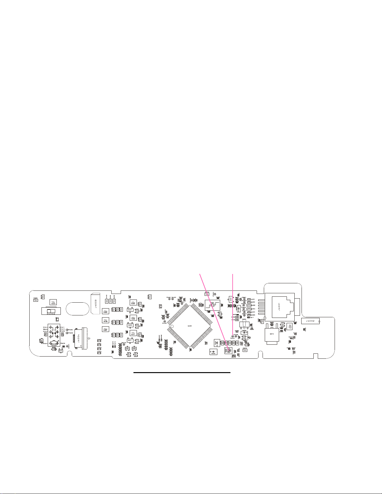
Local Oscillator Adjustment
Reference Frequency Adjustment
1. Connect an RF millivoltmeter or an oscilloscope to
pin 2 of J5002 on the REF Unit.
2. Confirm that the RF millivoltmeter reading is 115 mV
(± 30 mV) rms or 320 mV (± 90mV) p-p.
3. Connect the frequency counter to pin 2 of J5002 on
the REF Unit.
4. Adjust the TC5001 for 67.875000 MHz (±10 Hz) on
the frequency counter.
3rd Local Adjustment
1. Connect an RF millivoltmeter or an oscilloscope to
TP1037 on the MAIN Unit.
2. Key the transceiver on CW mode, and adjust T1025
for maximum indication on the RF millivoltmeter.
3. Confirm that the indicated voltage is 100 mV (± 30
mV) rms or 280 mV (± 80mV) p-p.
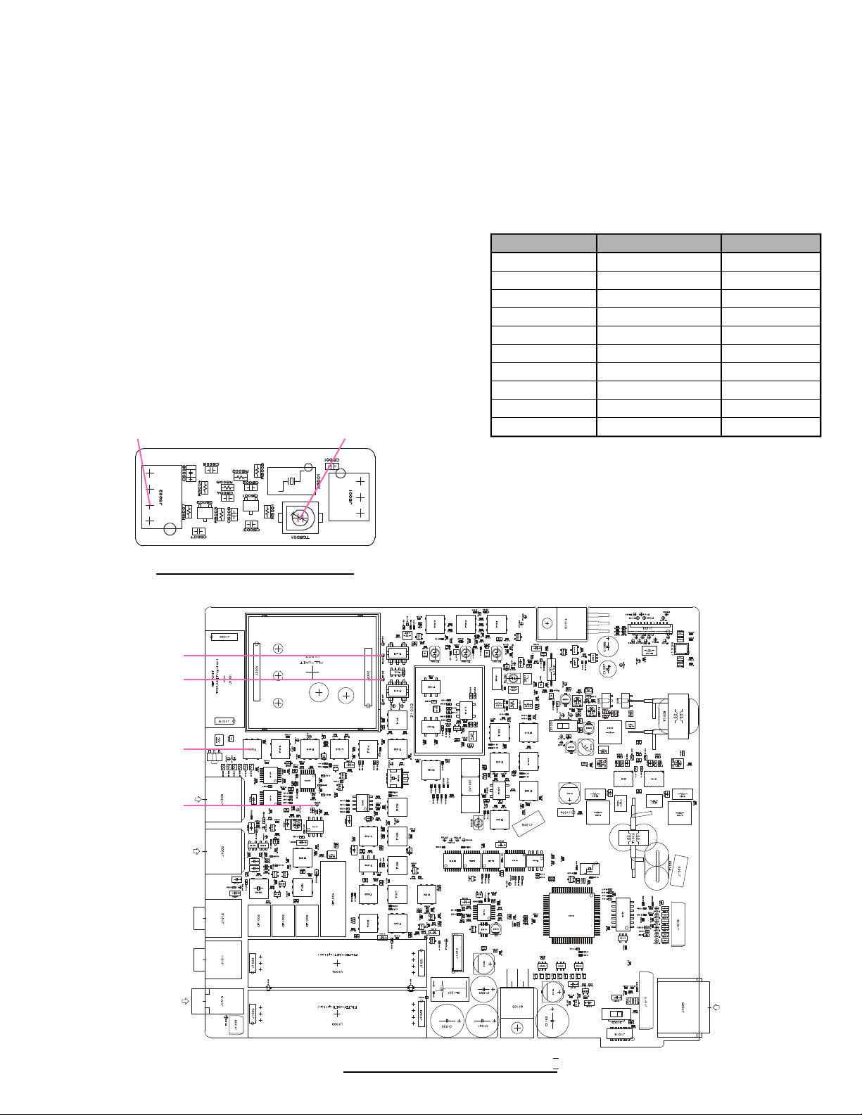
)
REF Unit Alignment Points
TC5001J5002 (pin 2
PLL Adjustment
VCO VCV Adjustment
1. Connect the DC voltmeter to TP1028 on the MAIN
Unit (or pin 6 of J2002 on the PLL Unit), and referring to the table below, tune the transformer/inductor
on the PLL Unit on each frequency listed. Then confirm that the correct voltage is present, or adjust the
listed component for the required voltage.
Tune to : Adjust / Confirm For
13.895 MHz Adjust T2001 5.5V ±0.5V
76.000 MHz Confirm At least 0.8V
32.995 MHz Adjust T2002 5.5V ±0.5V
19.900 MHz Confirm At least 0.8V
55.995 MHz Adjust T2003 5.5V ±0.5V
88.000 MHz Confirm At least 0.5V
163.995 MHz Adjust L2010 5.5V ±0.5V
118.000 MHz Confirm At least 0.5V
469.995 MHz Adjust L2011 5.5V ±0.5V
420.000 MHz Confirm At least 0.5V
1st Local Output Level
1. Connect the RF millivoltmeter to TP1029 on the
MAIN Unit (or pin 11 of J2002 on the PLL Unit), and
set the transceiver to 28.000 MHz.
2. Confirm that the RF level is at least 0 dBm or 200 mV
rms.
TP1029
TP1028
T1025
TP1037
MAIN Unit Alignment Points I
13
Alignment
GND
PTT
MIC
MIC GND
PLL Unlock
1. Connect the DC voltmeter to TP1029 on the MAIN
Unit (or pin 11 of J2002 on the PLL Unit).
2. Disconnect the REF Unit from the MAIN Unit; confirm that the DC voltmeter shows less than 0.5 V and
that “UNLOCK” is displayed on the LCD.
3. Re-connect the REF Unit to the MAIN Unit, and confirm that the DC voltmeter shows at least 3.5 V and
that the LCD returns to its normal display.
Idling Current Adjustment
Before alignment, set the mode to CW and tune the transceiver to 1.800 MHz. Nothing should be connected to the
CW Key Jack, and switch off S1001 on the MAIN Unit.
Pre-Driver Stage Idling Current
1. Connect the ammeter between TP1019 (+) and
TP1020 (–) on the MAIN Unit.
2. Press the PTT, and adjust VR1004 for an indication
of 35 mA (±2 mA) on the ammeter.
Driver Stage Idling Current
1. Connect the ammeter between TP1017 (+) and
TP1018 (–) on the MAIN Unit.
2. Press the PTT and adjust VR1003 for an indication of
30 mA (±2mA) on the ammeter.
Exciter Stage Idling Current
1. Disconnect the Jumper Plug from J1004 on the MAIN
Unit, then connect the ammeter to J1004 (pin 1: –,
pin 1: +).
2. Turn both VR1001 and VR1002 fully counterclockwise.
3. Press the PTT and adjust VR1002 for an indication of
100mA (±10 mA) on the ammeter.
4. Press the PTT and adjust VR1001 for an indication of
200mA (±10 mA) on the ammeter.
5. Re-connect the Jumper Plug to J1004 and switch on
S1001.
TX IF Adjustment
SSB/CW TX IF Adjustment
1. Tune the frequency to the 14 MHz band. Connect the
RF millivoltmeter to TP1033 on the MAIN Unit.
2. Disconnect the Coaxial Cable from J1002 and terminate J1002 into a 50-Ohm dummy load.
3. Inject a 1 kHz tone at 1 mV level to
the MIC jack.
4. Key the transmitter, and adjust T1033
for maximum indication on the RF
millivoltmeter.
5. Disconnect the 50-Ohm dummy load
and re-connect the Coaxial Cable to J1002.
T1021
T1014
L1049
T1023
VR1005
T1033
TP1027
TP1033
T1013
T1012 T1011
S1001
TP1017
VR1004
VR1003
TP1018
TP1019
TP1020
VR1002
VR1001
J1004
J1002
J1003
MAIN Unit Alignment Points II
14
Alignment
FM TX IF Adjustment
1. Tune the frequency to the 28 MHz band. Connect the
RF millivoltmeter to TP1033 on the MAIN Unit.
2. Disconnect the Coaxial Cable from J1002 and terminate J1002 into a 50-Ohm dummy load.
3. Key the transmitter in the FM mode, and adjust T1014,
T1023, and T1021 alternately for maximum indication on the RF millivoltmeter.
4. Connect the frequency counter to TP1033.
5. Key the transmitter in the FM mode without microphone input. Adjust L1049 for a reading of 68.3300
MHz (±100 Hz).
6. Disconnect the 50-Ohm dummy load and re-connect
the Coaxial Cable to J1002.
Carrier Balance Adjustment
1. Tune the frequency to the 14 MHz band. Disconnect
the Coaxial Cable from J1002 on the MAIN Unit.
2. Terminate J1002 into a 50-Ohm dummy load and connect a spectrum analyzer or a RF millivoltmeter at this
point.
3. Key the transmitter in the USB mode without microphone input. Adjust VR1005 for maximum carrier suppression on the spectrum analyzer or for minimum indication on the RF millivoltmeter.
4. Disconnect the 50-Ohm dummy load and the spectrum
analyzer or the RF millivoltmeter, and re-connect the
Coaxial Cable to J1002.
TX BPF Adjustment
VHF TX BPF Adjustment
1. Set the frequency to 145.995 MHz. Disconnect the
Coaxial Cable from J1002 on the MAIN Unit.
2. Connect the spectrum analyzer to J1002, which should
be terminated into a 50-Ohm dummy load.
3. Inject a 1 kHz tone at 1 mV level to the MIC jack.
4. Key the transceiver in the USB mode, and adjust
T1013, T1012, and T1011 alternately for maximum
indication on the spectrum analyzer.
5. Disconnect the 50-Ohm dummy load and the spectrum
analyzer, and re-connect the Coaxial Cable to J1002.
UHF TX BPF Adjustment
1. Set the frequency to 430.000 MHz. Disconnect the
Coaxial Cable from J1002 on the MAIN Unit.
2. Connect the spectrum analyzer to J1002, which should
be terminated into a 50-Ohm dummy load.
3. Inject a 1 kHz tone at 1 mV level to the MIC jack.
4. Key the transceiver in the USB mode, and adjust
TC1004, TC1003 and TC1002 alternately for maximum indication on the spectrum analyzer.
5. Disconnect the 50-Ohm dummy load and the spectrum
analyzer, and re-connect the Coaxial Cable to J1002.
TC1004 TC1002
TC1003
T1024
T1019
T1018
T1026
T1028
TP1044
T1029
T1030
T1034
T1035
T1027
T1036
T1037
TC1005
T1008
T1010
T1005
T1009
T1006
T1004
TC1001
T1031
TP1043
MAIN Unit Alignment Points III
15

Alignment
RX Adjustment
SSB IF Adjustment
1. Connect the signal generator to the HF/50 MHz antenna jack, and the AF milivoltmeter and the SINAD
meter to the speaker jack.
2. Tune the transceiver to 51.995 MHz, and switch off
the ATT and IPO feature. Inject a 51.995 MHz signal
from a signal generator at 0 dBµ output.
3. Adjust T1018, T1019, T1024, T1026, T1028,
T1030, T1035, T1036, T1037, T1034 and T1029
on the MAIN UNIT alternately for maximum indication on the AF milivoltmeter. Several passes may be
necessary, as the adjustments inter-react to some degree.
FM IF Adjustment
1. Connect the signal generator to the HF/50 MHz antenna jack.
2. Tune the transceiver to 51.995 MHz. Inject a 51.995
MHz signal from a signal generator at 5 dBµ output,
with 1 kHz AF FM modulation at ±3.5 kHz deviation.
3. Adjust T1024, T1026, and T1028 on the MAIN Unit
alternately for maximum level on the S-meter.
Air-Band Reception Adjustment
1. Connect the signal generator to the HF/50 MHz antenna jack, and the DC voltmeter to TP1044 on the
MAIN Unit.
2. Tune the transceiver to 128.000 MHz in the AM mode.
Inject a 128.000 MHz signal from the signal generator
at 20 dBµ output, with 30% AM modulation at 400 Hz
audio frequency.
3. Adjust T1005 and T1008 for minimum indication on
the DC voltmeter.
VHF Band Alignment
1. Connect the signal generator to the 144/430 MHz antenna jack, and the DC voltmeter to TP1044 on the
MAIN Unit.
2. Tune the transceiver to 145.995 MHz in the CW mode.
Inject a 145.995 MHz signal from a signal generator
at 20 dBµ output.
3. Adjust T1006, T1009, and T1010 alternately for mini-
mum indication on the DC voltmeter.
UHF Band Alignment
1. Connect the signal generator to the 144/430 MHz an-
tenna jack, and the DC voltmeter to TP1044 on the
MAIN Unit.
2. Tune the transceiver to 439.995 MHz in the CW mode.
Inject a 439.995 MHz signal from the signal generator
at 20 dBµ output.
3. Adjust TC1001 for minimum indication on the DC
voltmeter.
W-FM Reception Adjustment
1. Connect the signal generator to the 144/430 MHz antenna jack, and the SINAD meter to the speaker jack.
2. Tune the transceiver to 88.000 MHz. Inject an 88.000
MHz signal from the signal generator at 30dBu output, with ±22.5 kHz deviation FM modulation of a 1
kHz audio signal.
3. Adjust TC1005 for the best SINAD sensitivity. Then
reduce the output level of the signal generator to where
the signal just begins to sound slightly “noisy,” and
adjust TC1005 again for best SINAD.
Image Rejection Trap Adjustment
1. Connect the signal generator to the HF/50 MHz antenna jack, the AF millivoltmeter to the speaker jack.
2. Tune the transceiver to 51.995 MHz in the FM mode.
Inject a 68.330 MHz signal from a signal generator at
70 dBµ output, with 1 kHz AF FM modulation at ±3.5
kHz deviation
3. Adjust T1004 for minimum indication on the AF
millivoltmeter. Then increase the output level of the
signal generator slightly and adjust T1004 again, so
as to ensure maximum notching of the image.
Noise Blanker Adjustment
1. Connect the signal generator to the HF/50 MHz antenna jack, and the DC voltmeter to TP1043 on the
MAIN Unit.
2. Tune the transceiver to 51.995 MHz and inject a 51.995
MHz signal from the signal generator at 20 dBµ output.
3. Activate the noise blanker, and adjust T1027 and
T1031 for minimum indication on the DC voltmeter.
16
Alignment
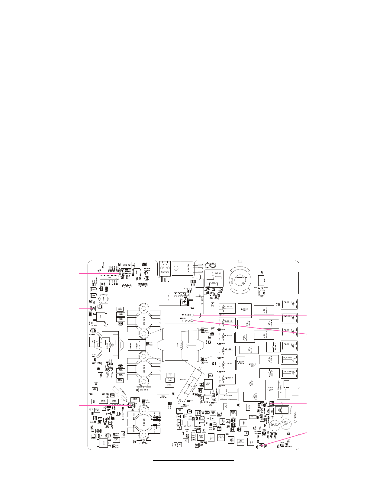
Power Amplifier Adjustment
HF/50 MHz Idling Current Adjustment
1. Connect the 50-Ohm dummy load to the HF/50 MHz
antenna jack.
2. Tune the transceiver to any HF band, or to the 50 MHz
band.
3. Disconnect the wire jumper from TP3025 and
TP3026 on the PA Unit, then connect the ammeter
between TP3025 (+) and TP3026 (–).
4. Turn VR3001 fully counterclockwise.
5. Press the PTT, and adjust VR3001 for an indication
of 300 mA (±10 mA) on the ammeter.
6. Disconnect the ammeter, and re-connect TP3025 and
TP3026 using the wire jumper.
V/UHF Idling Current Adjustment
1. Connect the 50-Ohm dummy load to the 144/430 MHz
antenna jack.
2. Tune the transceiver to the 430 MHz band.
3. Disconnect the wire jumper from TP3025 and
TP3026 on the PA Unit, then connect the ammeter
between TP3025 (+) and TP3026 (–).
4. Turn VR3002 fully counterclockwise.
5. Press the PTT, and adjust VR3002 for an indication
of 300 mA (±10 mA) on the ammeter.
6. Disconnect the ammeter, and re-connect TP3025 and
TP3026 using the wire jumper.
Directional Coupler Balance Adjustment
1. Connect the 50-Ohm dummy load to the HF/50 MHz
antenna jack.
2. Tune the transceiver to 28 MHz band in the CW mode,
and connect the DC voltmeter to TP3003 on the PA
Unit.
3. Press the PTT, and adjust TC3002 for minimum indication on the DC voltmeter.
4. Connect the 50-Ohm dummy load and wattmeter to
the 144/430 MHz antenna jack
5. Tune the transceiver to 439.995 MHz in the CW mode.
6. Press the PTT, and adjust VR3003 for minimum indication on the DC voltmeter.
7. Leave the transceiver on 439.995 MHz band and key
the transceiver.
8. Adjust TC3001 for maximum indication on the wattmeter.
TP3003
VR3001
TC3001
TP3025
TP3026
TC3002
VR3003
PA Unit Alignment Points
17
Alignment
LCD Contrast Alignment
1. Connect a DC voltmeter (High Impedance) to TP4027
on the PANEL Unit.
2. Adjust VR4001 for an indication of –2.54 V (±0.02
V) on the voltmeter.
Software Menu Alignment
The antenna jacks should be connected to a dummy load
(in cases where transmission is involved) or the signal
generator (in the case of reception). General alignment
conditions are as follows unless otherwise noted.
AF-gain knob: Center
RF-gain knob: Fully clockwise
SQL: Fully counterclockwise
ATT/IPO/CTCSS/DCS: Off
AGC: Auto
Output power: Max
Break-in: On,
CW Keyer: Off
VOX: Off
Press and hold in three Multi Function Keys ([A], [B],
[C])
simultaneously and turn on the transceiver while holding them in; the alignment menu will then be activated
(you will hear a “diddle-diddle-diddle” opening tone sequence to confirm that the alignment menu has been activated).
In the alignment procedures, each alignment parameter is
selected by rotating the main DIAL knob. Each Alignment item is then selected by rotating the SELECT knob.
To store the alignment parameters when you are satisfied
with the adjustment, press the [FUNC] key for longer than
a one second.
VR4001 TP4027
PANEL Unit Alignment Points
18
Alignment
RX Gain Adjustment
1. Tune the transceiver to the 1.8 MHz band in the CW
mode.
2. Select “HF1RXG” in the menu by rotating the SELECT
knob, if necessary.
3. Inject an RF signal from the signal generator at 9 dBµ
output.
4. Adjust the “HF1RXG” parameter by rotating the main
DIAL knob to the point where the S-meter indicates
“S1.”
5. The other RX gain adjustments (see the chart below)
should be performed in the same way. The output levels of the signal generator at each frequency are shown
below.
Menu Frequency Output Level of SG
01: HF1RXG 1.8 MHz Band 9 dBµ
02: HF2RXG 7 MHz Band 9 dBµ
03: HF3RXG 21 MHz Band 6 dBµ
04: 50MRXG 50 MHz Band 3 dBµ
05: VHFRXG 144 MHz Band 0 dBµ
06: UHFRXG 430 MHz Band 0 dBµ
SSB S-Meter Adjustment
1. Tune the transceiver to the 21 MHz band in the CW
mode.
2. Inject an RF signal from the signal generator at 36 dBµ
output.
3. Select menu item “07: SSB-S9” and press the [A] key
to set this parameter.
4. Increase the signal generator output level to 86 dBµ.
5. Select menu item “08: SSB-FS” and press the [A] key
to set this parameter.
FM S-Meter Adjustment
1. Tune the transceiver to the 144 MHz band in the FM
mode.
2. Inject an RF signal from the signal generator at 0 dBµ
output, with ±3.5 kHz deviation FM Modulation of a 1
kHz tone.
3. Select menu item “09: FM-S1” and press the [A] key
to set this parameter.
4. Increase the signal generator output level to 25 dBµ.
5. Select menu item “10: FM-FS” and press the [A] key
to set this parameter.
FM Center Meter Adjustment
1. Tune the transceiver to the 144 MHz band in the FM
mode.
2. Inject an RF signal from the signal generator at 10 dBµ
output, with ±3.5 kHz deviation FM Modulation of a 1
kHz tone.
3. Set the frequency of the signal generator 3 kHz below
the receiving frequency of the transceiver.
4. Select menu item “11: DISC-L” and press the [A] key
to set this parameter.
5. Set the frequency of the signal generator 3 kHz above
the receiving frequency of the transceiver.
6. Select menu item “12: DISC-H” and press the [A] key
to set this parameter.
FM Squelch Adjustment
1. Tune the transceiver to the 144 MHz band in the FM
mode. Confirm that the squelch knob is turned fully
counterclockwise.
2. Inject an RF signal from the signal generator at –15
dBµ output, with ±3.5 kHz deviation FM Modulation
of a 1 kHz tone.
3. Select menu item “13: FM-TH1” and press the [A] key
to set this parameter.
4. Select menu item “14: FM-TH2” and press the [A] key
again.
5. Increase the signal generator output level to 0 dBµ.
6. Select menu item “15: FM-TI1” and press the [A] key
to set this parameter.
7. Select menu item “16: FM-TI2” and press the [A] key
again.
Power Supply Voltage Display Adjustment
1. Tune the transceiver to the 144 MHz band in the FM
mode. Confirm that the power supply voltage is 13.8
V (±0.1 V).
2. Select menu item “17: VCC” and adjust this parameter such that “138” is displayed on the LCD.
19

Alignment
Over-current Protection Adjustment
1. Set the transceiver to the CW mode.
2. Select menu item “18: HF1-IC.” Tune the transceiver
to the 1.8 MHz band and key the transceiver. Adjust
this parameter for 140 Watts of transmission power.
3. Select menu item “19: HF2-IC.” Tune the transceiver
to the 7 MHz band and key the transceiver. Adjust this
parameter for 130 Watts of transmission power.
4. Select menu item “20: HF3-IC.” Tune the transceiver
to the 21 MHz band and key the transceiver. Adjust
this parameter for 130 Watts of transmission power.
5. Select menu item “21: 50M-IC.” Tune the transceiver
to the 50 MHz band and key the transceiver. Adjust
this parameter for 120 Watts of transmission power.
6. Select menu item “22: VHF-IC.” Tune the transceiver
to the 144 MHz band and key the transceiver. Adjust
this parameter for 60 Watts of transmission power.
7. Select menu item “23: UHF-IC.” Tune the transceiver
to 430.000 MHz and key the transceiver. Adjust this
parameter for 25 Watts of transmission power.
RF Power Adjustment
1. Tune the transceiver to the 1.8 MHz band in the CW
mode.
2. Select menu item “24: HF1-MAX.” Key the transmitter, and adjust this parameter for 100 Watts (±5 W) of
transmission power.
3. Select menu item “25: HF1-MID2.” Key the transmitter, and confirm that the output power is 50 W (± 5W).
In case the transmission power is not within the specified tolerance, adjust this parameter for 50 W (± 5 W)
of transmission power.
4. Select menu item “26: HF1-MID1.” Key the transmitter, and confirm that the output power is 10 W (± 1
W). In case the power is not within the specified tolerance, adjust this parameter for 10 W (±1 W) of transmission power.
5. Select menu item “27: HF1-MIN.” Key the transmitter, and confirm that the output power is 5 W (±1 W).
In case the power is not within the specified tolerance,
adjust this parameter for 5 W (±1 W) of transmission
power.
6. The other RF power adjustment menus, [HF2-**] and
[HF3-**], should be adjusted in the same manner as
shown above for the 7 MHz and 21 MHz bands respectively.
7. Tune the transceiver to the 50 MHz band in the CW
mode.
8. Select menu item “36: 50M-MAX.” Key the transmitter, and adjust this parameter for 100 W (±5 W) of
transmission power.
9. Select menu item “37: 50M-MID2.” Key the transmitter, and confirm that the output power is 50 W (±5
W). In case the transmission power is not within the
specified tolerance, adjust this parameter for 50 W (±5
W) of transmission power.
10.Select menu item “38: 50M-MID1.” Key the transmitter, and confirm that the output power is 20 W (±
2W). In case the power is not within the specified tolerance, adjust this parameter for 20 W (±2 W) of transmission power.
11.Select menu item “39: 50M-MIN.” Key the transmitter, and confirm that the output power is 5 W (+0/–1
W). In case the power is not within the specified tolerance, adjust this parameter for 5 W (+0/–1 W) of transmission power.
12.Tune the transceiver to the 144 MHz band in the CW
mode.
13.Select menu item “40: VHF-MAX.” Key the transmitter, and adjust this parameter for 50 W (±2.5 W) of
transmission power.
14.Select menu item “41: VHF-MID.” Key the transmitter, and confirm that the output power is 20 W (±2 W).
20

Alignment
In case the transmission power is not within the specified tolerance, adjust this parameter for 20 W (±2 W)
of transmission power.
15.Select menu item “42: VHF-MIN.” Key the transmit-
ter, and confirm that the output power is 5 W (+0/–1
W). In case the power is not within the specified tolerance, adjust this parameter for 5 W (+0/–1 W) of transmission power.
16.Tune the transceiver to the 430 MHz band in the CW
mode.
17.Select menu item “43: UHF-MAX.” Key the transmitter, and adjust this parameter for 20 W (±1 W) of transmission power.
18.Select menu item “44: UHF-MID.” Key the transmitter, and confirm that the output power is 20 W (±0.3
W). In case the transmission power is not within the
specified tolerance, adjust this parameter for 20 W
(±0.3 W) of transmission power.
TX Gain Adjustment
1. Set the transceiver to the USB mode.
2. Inject a 1 kHz tone at 1 mV level to the MIC jack.
3. Tune the transceiver to the 1.8 MHz band.
4. Select menu item “45: HF1TXG.” Key the transmitter,
and adjust this parameter for 70 W (±10 W) of transmission power.
5. The other TX gain adjustment menus, “46: HF2TXG,”
“47: HF3TXG,” and “48: 50MTXG,” should be adjusted in the same manner as detailed above on the 7
MHz, 21 MHz, and 50 MHz bands, respectively.
6. Tune the transceiver to the 144 MHz band.
7. Select menu item “49: VHFTXG.” Key the transmitter
and adjust this parameter for 35 W (±5 W) of transmission power.
8. Tune the transceiver to the 430 MHz band.
9. Select menu item “50: UHFTXG.” Key the transmitter
and adjust this parameter for 10 W (±2 W) of transmission power.
ALC (Automatic Level Control) Meter Adjustment
1. Tune the transceiver to the 21 MHz band in the USB
mode.
2. Select menu item “51: ALC-1.” Key the transceiver
without microphone input and press the [A] key. Now,
a value which the microprocessor computes will be
displayed on the LCD.
3. Rotate the main DIAL knob to adjust this parameter to
a reading four digits lower than the parameter value
displayed in the previous step.
4. After setting the parameter, confirm that all the dots of
the ALC meter have gone out.
5. Select menu item “52: ALC-M.” 1 kHz tone at 4 mV
level to the MIC jack.
6. Press the [A] key and confirm that the ALC meter
shows an “S-8” S-meter reading on the LCD.
AFP (Automatic Final Protection) Adjustment
1. Tune the transceiver to the 1.8 MHz band in the CW
mode, and connect a 150-Ohm dummy load to the antenna jack.
2. Select menu item “53: HF1-RV.” Key the transmitter,
and adjust this parameter for an “S-8” S-meter reading
on the LCD.
3. The other AFP adjustment menus, “54: HF2-RV,” “55:
HF3-RV,” and “56: 50M-RV,” should be adjusted in
the same manner as shown above on the 7 MHz, 21
MHz, and 50 MHz bands, respectively.
4. Tune the transceiver to the 144 MHz band.
5. Select menu item “57: VHF-RV.” Key the transmitter,
and adjust this parameter for an “S-6” S-meter reading
on the LCD.
6. Tune the transceiver to the 430 MHz band.
7. Select menu item “58: UHF-RV.” Key the transmitter,
and adjust this parameter for an “S-3” S-meter reading
on the LCD.
Carrier Level Adjustment
1. Tune the transceiver to the 21 MHz band in the CW
mode.
2. Connect a 50-Ohm dummy load to the HF/50MHz
antenna jack.
8. Select menu item “59: CW-CAR.” Key the transmitter, and adjust this parameter for an “S-9” S-meter reading on the LCD.
3. Connect the oscilloscope to the HF/50MHz antenna
jack via an appropriate attenuator.
4. Set the transceiver to the AM mode.
5. Inject a 1 kHz tone at 1 mV level to the MIC jack.
6. Select menu item “60: AM-CAR.” Key the transmitter,
and adjust this parameter for 33% AM modulation on
the oscilloscope.
21

Alignment
FM Modulation Adjustment
1. Tune the transceiver to the 144 MHz band in the FM
mode. Connect the FM linear detector to the 144/430
MHz antenna jack via an appropriate attenuator.
2. Inject a 1 kHz tone at 15 mV level to the MIC jack.
3. Select menu item “61: DEV-W.” Key the transmitter,
and adjust this parameter for a maximum deviation of
±4.5 kHz (±0.2 kHz) on the FM linear detector.
4. Select menu item to “62: DEV-N.” Key the transmitter, and adjust this parameter for maximum deviation
of ±2.25 kHz (±0.1 kHz) on the FM linear detector.
5. Select menu item to “63: M-MTR.” Key the transmitter, and set this parameter for an “S-9” indication on
the S-meter on the LCD.
6. Select menu item to “64: DTMF.” Key the transmitter,
and adjust this parameter for a maximum deviation of
±3.5 kHz (±0.3 kHz) on the FM linear detector (the
transceiver generates the DTMF “D” tone automatically while the menu item selected is “64: DTMF”).
7. Select menu item to “65: CTCSS.” Key the transmitter without microphone input, and adjust this parameter for a maximum deviation of ±0.7 kHz (±0.1 kHz)
on the FM linear detector (the transceiver generates a
CTCSS tone automatically while the menu item selected is “65: CTCSS”).
8. Select menu item to “66: DCS.” Key the transmitter
without microphone input, and adjust this parameter
for a maximum deviation of ±0.7 kHz (±0.2 kHz) on
the FM linear detector (the transceiver generates a DCS
tone automatically while the menu item selected is “66:
DCS”).
SSB Carrier Point Adjustment
1. Tune the transceiver to the 21 MHz band in the LSB
mode.
2. Connect a 50-Ohm dummy load and wattmeter to the
HF/50MHz antenna jack.
3. Inject a 400 Hz tone at 1 mV level to the MIC jack.
4. Select menu item “67: LSB-CP.” Key the transmitter,
and adjust the audio generator output so that the transmission power is 20 Watts.
5. Change the audio frequency to 2600 Hz. Key the transmitter, and adjust this parameter so that the transmission power is 20 W (±2 W).
6. The adjustment for the USB carrier point is performed
in the same manner as done for LSB by changing the
transmission mode to USB and the menu item to “68:
USB-CP.”
VSWR Adjustment
1. Connect a 100-Ohm dummy load to the HF/50 MHz
antenna jack.
2. Tune the transceiver to the 14 MHz band in the CW
mode, and set the output power to 10 Watts.
3. Select menu item “69: SWR2.” Key the transceiver
and press the [A] key to set this parameter.
4. Connect a 150-Ohm dummy load to the HF/50 MHz
antenna jack, and set the output power to 10 Watts.
5. Select menu item “70: SWR3”. Key the transceiver
and press the [A] key to set this parameter.
ATAS control voltage confirmation
1. Connect the DC voltmeter to the HF/50 MHz antenna
jack.
2. Select menu item “71: ATAS.”
3. Press the [A] key, and confirm that the voltage is 9.0 to
10.1 Volts.
4. Press the [B] key, and confirm that the voltage is 7.5
to 8.5 Volts.
5. Press the [C] key, and confirm that the voltage is more
than 10.5 Volts.
22
This completes the internal alignment routine for all bands.
To save all settings and exit, press and hold in the [FUNC
key for at least one second.
]
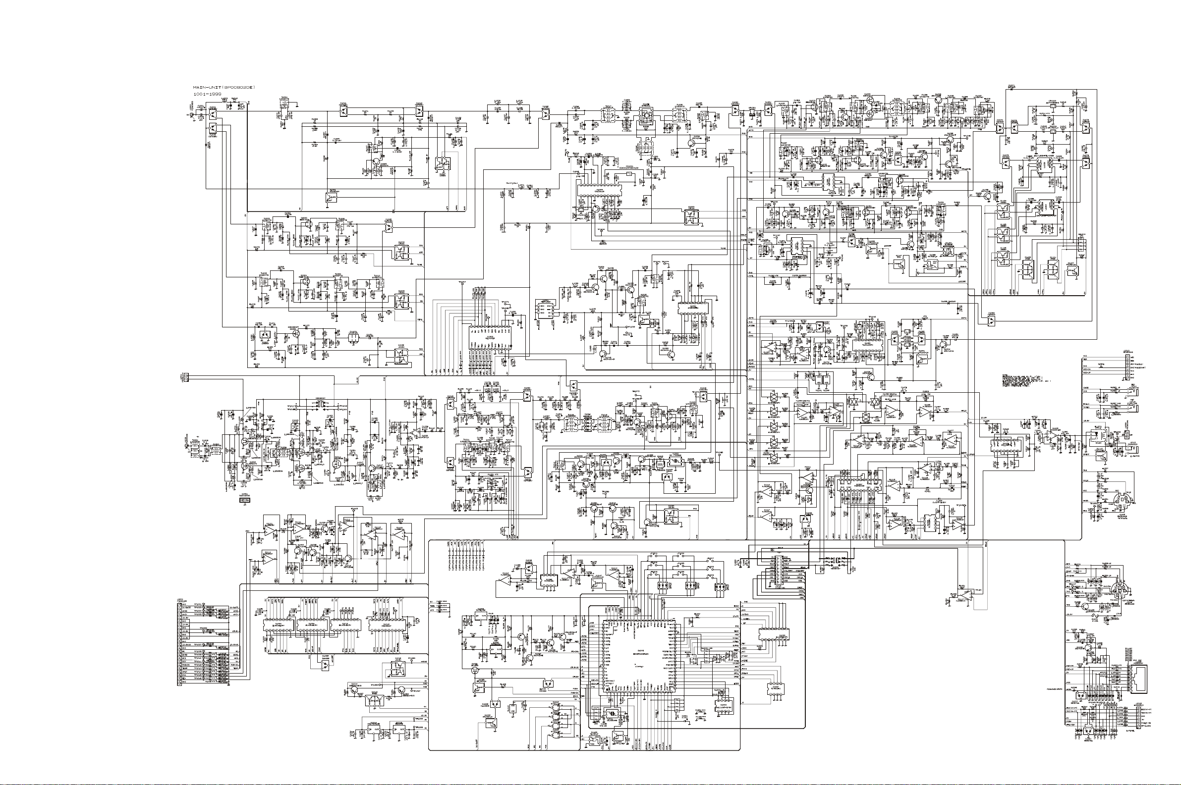
MAIN Unit
Circuit Diagram
23

MAIN Unit
Note:
24
MAIN Unit
Parts Layout
BA DC FE G H
HD64F2134FA20
(Q1049)
24LC128T
(Q1065)
TC4W53FU
(Q1038)
2SK2973 (K1)
(Q1006, 1007)
BU4066BCFV-E2
(Q1121, 1122)
BU4094BCFV-E2
(Q1003, 1004, 1010)
NJM2902V
(Q1114, 1120)
SA602AD
(Q1071, 1082)
2SA1602A (MF)
(Q1036)
2SB624 (BV3)
(Q1013, 1020)
KIA7808API
(Q1014)
2SC4154E (LE)
(Q1037, 1057,
1064, 1069,
1077, 1085,
1090, 1093)
M62352GP
(Q1016)
TDA2003H
(Q1105)
2SD2211 (DQR)
(Q1108)
BU4011BF
(Q1113)
2SK2975
(Q1001, 1002)
DTC114EU (24)
(Q1053)
1
2
3
FMG5 (G5)
(Q1015)
TC4S81F (C2)
(Q1129)
1SS372 (N9)
(D1061, 1064)
DA221 (K)
(D1043)
RT1N241M (N2)
(Q1047, 1086)
UMC5N (C5)
(Q1018, 1060)
DAN222 (N)
(D1083)
SPM5001
(Q1128)
UMH6N (H6)
(Q1124)
DAP222 (P)
(D1079)
DAP236U (X)
(D1019, 1031)
TA75S01F (SA)
(Q1095)
HSB88WSTR
(D1034)
TC4S66F (C9)
(Q1100)
IMN10 (N10)
(D1044, 1047,
1048)
4
5
6
7
MC2850 (A7)
(D1032)
Side A
25
 Loading...