

Page 1

0
R
DS056 (v1.9) March 22, 2006
00
Features
• 5 ns pin-to-pin logic delays
• System frequency up to 178 MHz
• 144 macrocells with 3,200 usable gates
• Available in small footprint packages
- 100-pin TQFP (81 user I/O pins)
- 144-pin TQFP (117 user I/O pins)
- 144-CSP (117 user I/O pins)
- Pb-free available for all packages
• Optimized for high-performance 3.3V systems
- Low power operation
- 5V tolerant I/O pins accept 5V, 3.3V, and 2.5V
signals
- 3.3V or 2.5V output capability
- Advanced 0.35 micron feature size CMOS
Fast FLASH™ technology
• Advanced system features
- In-system programmable
- Superior pin-locking and routability with
Fast CONNECT™ II switch matrix
- Extra wide 54-input Function Blocks
- Up to 90 product-terms per macrocell with
individual product-term allocation
- Local clock inversion with three global and one
product-term clocks
- Individual output enable per output pin with local
inversion
- Input hysteresis on all user and boundary-scan pin
inputs
- Bus-hold circuitry on all user pin inputs
- Full IEEE Standard 1149.1 boundary-scan (JTAG)
• Fast concurrent programming
• Slew rate control on individual outputs
• Enhanced data security features
• Excellent quality and reliability
- Endurance exceeding 10,000 program/erase
cycles
- 20 year data retention
- ESD protection exceeding 2,000V
• Pin-compatible with 5V-core XC95144 device in the
100-pin TQFP package
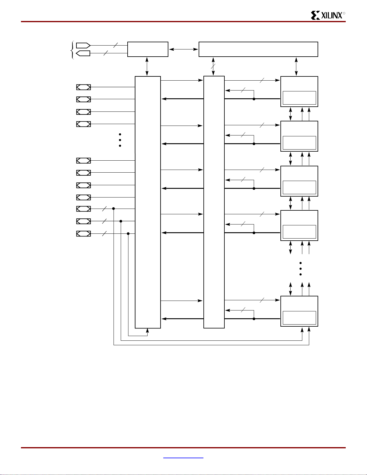
Description
The XC95144XL is a 3.3V CPLD targeted for high-performance, low-voltage applications in leading-edge communications and computing systems. It is comprised of eight
54V18 Function Blocks, providing 3,200 usable gates with
propagation delays of 5 ns. See Figure 2 for overview.
XC95144XL High Performance
CPLD
Product Specification
Power Estimation
Power dissipation in CPLDs can vary substantially depending on the system frequency, design application and output
loading. To help reduce power dissipation, each macrocell
in a XC9500XL device may be configured for low-power
mode (from the default high-performance mode). In addition, unused product-terms and macrocells are automatically deactivated by the software to further conserve power.
For a general estimate of I
used:
(mA) = MCHS(0.175*PT
I
CC
+ 0.272) + 0.04 * MC
where:
MC
= # macrocells in high-speed configuration
HS
PT
= average number of high-speed product terms
HS
per macrocell
= # macrocells in low power configuration
MC
LP
PT
= average number of low power product terms per
LP
macrocell
f = maximum clock frequency
MCTOG = average % of flip-flops toggling per clock
(~12%)
This calculation was derived from laboratory measurements
of an XC9500XL part filled with 16-bit counters and allowing
a single output (the LSB) to be enabled. The actual I
value varies with the design application and should be verified during normal system operation. Figure 1 shows the
above estimation in a graphical form. For a more detailed
discussion of power consumption in this device, see Xilinx
application note XAPP114, “Understanding XC9500XL
CPLD Power.”
250
200
150
(mA)
CC
100
Typical I
50
0
High Performance
P
Low
50 150
Figure 1: Typical ICC vs. Frequency for XC95144XL
, the following equation may be
CC
+ 0.345) + MCLP(0.052*PTLP
HS
(MCHS +MCLP)* f
TOG
178 MHz
104 MHz
r
owe
100 200
Clock Frequency (MHz)
CC
© 2006 Xilinx, Inc. All rights reserved. All Xilinx trademarks, registered trademarks, patents, and disclaimers are as listed at http://www.xilinx.com/legal.htm.
All other trademarks and registered trademarks are the property of their respective owners. All specifications are subject to change without notice.
DS056 (v1.9) March 22, 2006 www.xilinx.com 1
Product Specification
Page 2
XC95144XL High Performance CPLD
R
JTAG Port
I/O/GCK
I/O/GSR
I/O/GTS
I/O
I/O
I/O
I/O
I/O
I/O
I/O
I/O
3
1
JTAG
Controller
In-System Programming Controller
54
18
Function
Block 1
Macrocells
1 to 18
54
18
Function
Block 2
Macrocells
I/O
1 to 18
Blocks
54
18
Function
Block 3
Macrocells
Fast CONNECT II Switch Matrix
1 to 18
3
1
18
4
54
Function
Block 4
Macrocells
1 to 18
54
18
Function
Block 8
Macrocells
1 to 18
DS056_02_101300
Figure 2: XC95144XL Architecture
Function Block outputs (indicated by the bold line) drive the I/O Blocks directly.
2 www.xilinx.com DS056 (v1.9) March 22, 2006
Product Specification
Page 3

R
XC95144XL High Performance CPLD
Absolute Maximum Ratings
(2)
Symbol Description Value Units
V
CC
V
IN
V
TS
T
STG
T
J
Notes:
1. Maximum DC undershoot below GND must be limited to either 0.5V or 10 mA, whichever is easier to achieve. During transitions, the
device pins may undershoot to –2.0 V or overshoot to +7.0V, provided this over- or undershoot lasts less than 10 ns and with the
forcing current being limited to 200 mA. External I/O voltage may not exceed V
2. Stresses beyond those listed under Absolute Maximum Ratings may cause permanent damage to the device. These are stress
ratings only, and functional operation of the device at these or any other conditions beyond those listed under Operating Conditions
is not implied. Exposure to Absolute Maximum Ratings conditions for extended periods of time may affect device reliability.
3. For soldering guidelines and thermal considerations, see the Device Packaging information on the Xilinx website. For Pb-free
packages, see XAPP427.
Supply voltage relative to GND –0.5 to 4.0 V
Input voltage relative to GND
Voltage applied to 3-state output
Storage temperature (ambient)
Junction temperature +150
(1)
(3)
(1)
CCINT
by 4.0V.
–0.5 to 5.5 V
–0.5 to 5.5 V
–65 to +150
o
o
C
C
Recommended Operation Conditions
Symbol Parameter Min Max Units
V
CCINT
V
CCIO
V
V
V
IL
IH
O
Supply voltage for internal logic
and input buffers
Commercial TA = 0oC to 70oC3.0 3.6 V
Industrial T
= –40oC to +85oC3.0 3.6 V
A
Supply voltage for output drivers for 3.3V operation 3.0 3.6 V
Supply voltage for output drivers for 2.5V operation 2.3 2.7 V
Low-level input voltage 0 0.80 V
High-level input voltage 2.0 5.5 V
Output voltage 0 V
CCIO
V
Quality and Reliability Characteristics
Symbol Parameter Min Max Units
V
T
N
ESD
DR
PE
Data Retention 20 - Years
Program/Erase Cycles (Endurance) 10,000 - Cycles
Electrostatic Discharge (ESD) 2,000 - Volts
DC Characteristic Over Recommended Operating Conditions
Symbol Parameter Test Conditions Min Max Units
V
OH
V
OL
I
IL
I
IH
Output high voltage for 3.3V outputs IOH = –4.0 mA 2.4 - V
Output high voltage for 2.5V outputs I
= –500 μA90% V
OH
CCIO
-V
Output low voltage for 3.3V outputs IOL = 8.0 mA - 0.4 V
Output low voltage for 2.5V outputs I
Input leakage current VCC = Max; VIN = GND or V
I/O high-Z leakage current VCC = Max; VIN = GND or V
= 500 μA-0.4V
OL
CC
CC
-±10μA
-±10μA
DS056 (v1.9) March 22, 2006 www.xilinx.com 3
Product Specification
Page 4

XC95144XL High Performance CPLD
Symbol Parameter Test Conditions Min Max Units
C
I
I
CC
IH
IN
I/O high-Z leakage current VCC = Max; V
V
= GND or 3.6V
IN
V
Min < VIN < 5.5V - ±50 μA
CC
CCIO
= Max;
-±10μA
I/O capacitance VIN = GND; f = 1.0 MHz - 10 pF
Operating supply current
VIN = GND, No load; f = 1.0 MHz 45 (Typical) mA
(low power mode, active)
AC Characteristics
XC95144XL-5 XC95144XL-7 XC95144XL-10
Symbol Parameter
T
PD
T
SU
T
H
T
CO
f
SYSTEM
T
PSU
T
PH
T
PCO
T
OE
T
OD
T
POE
T
POD
T
AO
T
PAO
T
WLH
T
APRPW
T
PLH
I/O to output valid - 5.0 - 7.5 - 10.0 ns
I/O setup time before GCK 3.7 - 4.8 - 6.5 - ns
I/O hold time after GCK 0 - 0 - 0 - ns
GCK to output valid - 3.5 - 4.5 - 5.8 ns
Multiple FB internal operating frequency - 178.6 - 125.0 - 100.0 MHz
I/O setup time before p-term clock input 1.7 - 1.6 - 2.1 - ns
I/O hold time after p-term clock input 2.0 - 3.2 - 4.4 - ns
P-term clock output valid - 5.5 - 7.7 - 10.2 ns
GTS to output valid - 4.0 - 5.0 - 7.0 ns
GTS to output disable - 4.0 - 5.0 - 7.0 ns
Product term OE to output enabled - 7.0 - 9.5 - 11.0 ns
Product term OE to output disabled - 7.0 - 9.5 - 11.0 ns
GSR to output valid - 10.0 - 12.0 - 14.5 ns
P-term S/R to output valid - 10.5 - 12.6 - 15.3 ns
GCK pulse width (High or Low) 2.8 - 4.0 - 4.5 - ns
Asynchronous preset/reset pulse width
5.0 - 6.5 - 7.0 - ns
(High or Low)
P-term clock pulse width (High or Low) 5.0 - 6.5 - 7.0 - ns
R
UnitsMin Max Min Max Min Max
V
TEST
R
Device Output
1
C
R
2
L
Output Type V
V
CCIO
3.3V
2.5V
TEST
3.3V
2.5V
R
1
320 Ω
250 Ω
R
2
360 Ω
660 Ω
C
L
35 pF
35 pF
DS058_03_081500
Figure 3: AC Load Circuit
4 www.xilinx.com DS056 (v1.9) March 22, 2006
Product Specification
Page 5

R
Internal Timing Parameters
XC95144XL High Performance CPLD
XC95144XL-5 XC95144XL-7 XC95144XL-10
Symbol Parameter
Buffer Delays
T
T
T
T
T
GCK
GSR
GTS
OUT
T
EN
Input buffer delay - 1.5 - 2.3 - 3.5 ns
IN
GCK buffer delay - 1.1 - 1.5 - 1.8 ns
GSR buffer delay - 2.0 - 3.1 - 4.5 ns
GTS buffer delay - 4.0 - 5.0 - 7.0 ns
Output buffer delay - 2.0 - 2.5 - 3.0 ns
Output buffer enable/disable
delay
Product Term Control Delays
T
PTCK
T
PTSR
T
PTTS
Product term clock delay - 1.6 - 2.4 - 2.7 ns
Product term set/reset delay - 1.0 - 1.4 - 1.8 ns
Product term 3-state delay - 5.5 - 7.2 - 7.5 ns
Internal Register and Combinatorial Delays
T
PDI
T
SUI
T
T
ECSU
T
ECHO
T
COI
T
AOI
T
RAI
T
LOGI
T
LOGILP
Combinatorial logic propagation delay - 0.5 - 1.3 - 1.7 ns
Register setup time 2.3 - 2.6 - 3.0 - ns
Register hold time 1.4 - 2.2 - 3.5 - ns
HI
Register clock enable setup time 2.3 - 2.6 - 3.0 - ns
Register clock enable hold time 1.4 - 2.2 - 3.5 - ns
Register clock to output valid time - 0.4 - 0.5 - 1.0 ns
Register async. S/R to output delay - 6.0 - 6.4 - 7.0 ns
Register async. S/R recover before clock 5.0 7.5 10.0 ns
Internal logic delay - 1.0 - 1.4 - 1.8 ns
Internal low power logic delay - 5.0 - 6.4 - 7.3 ns
Feedback Delays
UnitsMin Max Min Max Min Max
-0-0-0ns
T
Fast CONNECT II feedback delay - 1.9 - 3.5 - 4.2 ns
F
Time Adders
T
PTA
T
SLEW
DS056 (v1.9) March 22, 2006 www.xilinx.com 5
Product Specification
Incremental product term allocator delay - 0.7 - 0.8 - 1.0 ns
Slew-rate limited delay - 3.0 - 4.0 - 4.5 ns
Page 6

XC95144XL High Performance CPLD
R
XC95144XL I/O Pins
Function
Block
Macro-
cell TQ100 TQ144 CS144
(2)
BScan
Order
Function
Block
Macro-
cell TQ100 TQ144 CS144
BScan
Order
11-23H342931-39M3321
121116F142632
(1)
23
(1)
32
(1)
L1
(1)
318
1 3 12 17 G2 423 3 3 - 41 K4 315
14-25J142034-44N4312
1 5 13 19 G3 417 3 5 24 33 L2 309
1 6 14 20 G4 414 3 6 25 34 L3 306
17---411 37-46L5303
1 8 15 21 H1 408 3 8
(1)
27
(1)
38
(1)
N2
(1)
300
1 9 16 22 H2 405 3 9 28 40 N3 297
1 10 - 31 K3 402 3 10 - 48 N5 294
1111724H4399 3112943M4291
1121826J2396 3123045K5288
1 13 - - - 393 3 13 - - - 285
1141927J3390 3143249K6282
1152028J4387 3153350L6279
1 16 - 35 M1 384 3 16 - - - 276
117
(1)
22
(1)
30
(1)
K2
(1)
381 3 17 34 51 M6 273
1 18 - - - 378 3 18 - - - 270
2 1 - 142 C3 375 4 1 - 118 C9 267
22
(1)
99
(1)
143
(1)
A2
(1)
372 4 2 87 126 A7 264
23---369 43-133A5261
2 4 - 4 C1 366 4 4 - - - 258
25
26
(1)
(1)
(1)
1
(1)
2
(1)
2
(1)
3
B1
C2
(1)
(1)
363 4 5 89 128 D7 255
360 4 6 90 129 A6 252
27---357 47---249
28
29
(1)
(1)
(1)
3
(1)
4
(1)
5
(1)
6
D4
D3
(1)
(1)
354 4 8 91 130 B6 246
351 4 9 92 131 C6 243
2 10 - 7 D2 348 4 10 - 135 C5 240
21169E4345 41193132D6237
2 12 7 10 E3 342 4 12 94 134 B5 234
2 13 - 12 E1 339 4 13 - 137 A4 231
2 14 8 11 E2 336 4 14 95 136 D5 228
2 15 9 13 F4 333 4 15 96 138 B4 225
2 16 - 14 F3 330 4 16 - 139 C4 222
2 17 1015F2327 4 17 97140A3219
2 18 - - - 324 4 18 - - - 216
Notes:
1. Global control pin.
2. The pin-outs are the same for Pb-free versions of packages.
6 www.xilinx.com DS056 (v1.9) March 22, 2006
Product Specification
Page 7

R
XC95144XL (Continued)
XC95144XL High Performance CPLD
Function
Block
Macro-
cell TQ100 TQ144 CS144
BScan
Order
Function
Block
Macro-
cell TQ100 TQ144 CS144
BScan
Order
5 1 ---213 7 1 ---105
5 2 35 52 N6 210 7 2 50 71 N12 102
53-59L8207 73-75L1299
5 4 ---204 7 4 ---96
5 5 36 53 M7 201 7 5 52 74 M13 93
5 6 37 54 N7 198 7 6 53 76 L13 90
5 7 - 66 M10 195 7 7 - 77 K10 87
5 8 39 56 K7 192 7 8 54 78 K11 84
5 9 40 57 N8 189 7 9 55 80 K13 81
5 10 –- 68 N11 186 7 10 - 79 K12 78
5114158M8183 7115682J1175
5 124260K8180 7 125885H1072
5 13 - 70 L11 177 7 13 - 81 J10 69
5 144361N9174 7 145986H1166
5 154664K9171 7 156087H1263
5 16 - - - 168 7 16 - 83 J12 60
5 17 49 69 M11 165 7 17 61 88 H13 57
5 18 ---162 7 18 ---54
6 1 ---159 8 1 ---51
6 2 74 106 C11 156 8 2 63 91 G11 48
6 3 ---153 8 3 -95F1145
64-111B11150 84-97E1342
6 5 76 110 A12 147 8 5 64 92 G10 39
6 6 77 112 A11 144 8 6 65 93 F13 36
6 7 ---141 8 7 ---33
6 8 78 113 D10 138 8 8 66 94 F12 30
6 9 79 116 A10 135 8 9 67 96 F10 27
6 10 - 115 B10 132 8 10 - 101 D13 24
6 11 80 119 B9 129 8 11 68 98 E12 21
6 12 81 120 A9 126 8 12 70 100 E10 18
6 13 - - - 123 8 13 - 103 D11 15
6 14 82 121 D8 120 8 14 71 102 D12 12
6 15 85 124 A8 117 8 15 72 104 C13 9
6 16-117D9114 8 16-107B136
6 1786125B7111 8 1773105C123
6 18 ---108 8 18 ---0
Notes:
1. The pin-outs are the same for Pb-free versions of packages.
DS056 (v1.9) March 22, 2006 www.xilinx.com 7
Product Specification
Page 8

XC95144XL High Performance CPLD
R
XC95144XL Global, JTAG and Power Pins
(1)
Pin Type TQ100 TQ144 CS144
I/O/GCK1 22 30 K2
I/O/GCK2 23 32 L1
I/O/GCK3 27 38 N2
I/O/GTS1 3 5 D4
I/O/GTS2 4 6 D3
I/O/GTS3 1 2 B1
I/O/GTS4 2 3 C2
I/O/GSR 99 143 A2
TCK 48 67 L10
TDI4563L9
TDO 83 122 C8
TMS 47 65 N10
V
3.3V 5, 57, 98 8, 42, 84, 141 B3, D1, J13, L4
CCINT
V
2.5V/3.3V 26, 38, 51, 88 1, 37, 55, 73, 109, 127 A1, A13, C7, L7, N1, N13
CCIO
GND 21, 31, 44, 62, 69, 75, 84, 100 18, 29, 36, 47, 62, 72, 89, 90, 99,
108, 114, 123, 144
B2, B8, B12, C10, E11, G1, G12,
G13, K1, M2, M5, M9, M12
No Connects - – –
Notes:
1. The pin-outs are the same for Pb-free versions of packages.
8 www.xilinx.com DS056 (v1.9) March 22, 2006
Product Specification
Page 9

R
XC95144XL High Performance CPLD
Device Part Marking and Ordering Combination Information.
R
Device Type
Package
XC95xxxXL
TQ144
This line not
Speed
Operating Range
7C
1
Sample package with part marking.
related to device
part number
Speed
Device Ordering and
Part Marking Number
(pin-to-pin
delay)
Pkg.
Symbol
No. of
Pins Package Type
Operating
Range
XC95144XL-5TQ100C 5 ns TQ100 100-pin Thin Quad Flat Pack (TQFP) C
XC95144XL-5TQ144C 5 ns TQ144 144-pin Thin Quad Flat Pack (TQFP) C
XC95144XL-5CS144C 5 ns CS144 144-ball Chip Scale Package (CSP) C
XC95144XL-7TQ100C 7.5 ns TQ100 100-pin Thin Quad Flat Pack (TQFP) C
XC95144XL-7TQ144C 7.5 ns TQ144 144-pin Thin Quad Flat Pack (TQFP) C
XC95144XL-7CS144C 7.5 ns CS144 144-ball Chip Scale Package (CSP) C
XC95144XL-7TQ100I 7.5 ns TQ100 100-pin Thin Quad Flat Pack (TQFP) I
(1)
XC95144XL-7TQ144I 7.5 ns TQ144 144-pin Thin Quad Flat Pack (TQFP) I
XC95144XL-7CS144I 7.5 ns CS144 144-ball Chip Scale Package (CSP) I
XC95144XL-10TQ100C 10 ns TQ100 100-pin Thin Quad Flat Pack (TQFP) C
XC95144XL-10TQ144C 10 ns TQ144 144-pin Thin Quad Flat Pack (TQFP) C
XC95144XL-10CS144C 10 ns CS144 144-ball Chip Scale Package (CSP) C
XC95144XL-10TQ100I 10 ns TQ100 100-pin Thin Quad Flat Pack (TQFP) I
XC95144XL-10TQ144I 10 ns TQ144 144-pin Thin Quad Flat Pack (TQFP) I
XC95144XL-10CS144I 10 ns CS144 144-ball Chip Scale Package (CSP) I
XC95144XL-5TQG100C 5 ns TQG100 100-pin Thin Quad Flat Pack (TQFP); Pb-free C
XC95144XL-5TQG144C 5 ns TQG144 144-pin Thin Quad Flat Pack (TQFP); Pb-free C
XC95144XL-5CSG144C 5 ns CSG144 144-ball Chip Scale Package (CSP); Pb-free C
XC95144XL-7TQG100C 7.5 ns TQG100 100-pin Thin Quad Flat Pack (TQFP); Pb-free C
XC95144XL-7TQG144C 7.5 ns TQG144 144-pin Thin Quad Flat Pack (TQFP); Pb-free C
XC95144XL-7CSG144C 7.5 ns CSG144 144-ball Chip Scale Package (CSP); Pb-free C
XC95144XL-7TQG100I 7.5 ns TQG100 100-pin Thin Quad Flat Pack (TQFP); Pb-free I
XC95144XL-7TQG144I 7.5 ns TQG144 144-pin Thin Quad Flat Pack (TQFP); Pb-free I
XC95144XL-7CSG144I 7.5 ns CSG144 144-ball Chip Scale Package (CSP); Pb-free I
DS056 (v1.9) March 22, 2006 www.xilinx.com 9
Product Specification
Page 10

XC95144XL High Performance CPLD
Speed
Device Ordering and
Part Marking Number
(pin-to-pin
delay)
Pkg.
Symbol
No. of
Pins Package Type
Operating
Range
XC95144XL-10TQG100C 10 ns TQG100 100-pin Thin Quad Flat Pack (TQFP); Pb-free C
XC95144XL-10TQG144C 10 ns TQG144 144-pin Thin Quad Flat Pack (TQFP); Pb-free C
XC95144XL-10CSG144C 10 ns CSG144 144-ball Chip Scale Package (CSP); Pb-free C
XC95144XL-10TQG100I 10 ns TQG100 100-pin Thin Quad Flat Pack (TQFP); Pb-free I
XC95144XL-10TQG144I 10 ns TQG144 144-pin Thin Quad Flat Pack (TQFP); Pb-free I
XC95144XL-10CSG144I 10 ns CSG144 144-ball Chip Scale Package (CSP); Pb-free I
Notes:
1. C = Commercial: T
= 0° to +70°C; I = Industrial: TA = –40° to +85°C
A
R
(1)
Standard Example: XC95144XL
Device
Speed Grade
Package Type
Number of Pins
Temperature Range
-4 TQ C144
Pb-
Device
Speed Grade
Package Type
-Free
Pb
Number of Pins
Free Example:
XC95144XL
TQ G 144 C
-4
Temperature Range
Warranty Disclaimer
THESE PRODUCTS ARE SUBJECT TO THE TERMS OF THE XILINX LIMITED WARRANTY WHICH CAN BE VIEWED
AT http://www.xilinx.com/warranty.htm
. THIS LIMITED WARRANTY DOES NOT EXTEND TO ANY USE OF THE
PRODUCTS IN AN APPLICATION OR ENVIRONMENT THAT IS NOT WITHIN THE SPECIFICATIONS STATED ON THE
THEN-CURRENT XILINX DATA SHEET FOR THE PRODUCTS. PRODUCTS ARE NOT DESIGNED TO BE FAIL-SAFE
AND ARE NOT WARRANTED FOR USE IN APPLICATIONS THAT POSE A RISK OF PHYSICAL HARM OR LOSS OF
LIFE. USE OF PRODUCTS IN SUCH APPLICATIONS IS FULLY AT THE RISK OF CUSTOMER SUBJECT TO
APPLICABLE LAWS AND REGULATIONS.
Further Reading
The following Xilinx links go to relevant XC9500XL CPLD documentation, including XAPP111, Using the XC9500XL Timing
Model, and XAPP784, Bulletproof CPLD Design Practices. Simply click on the link and scroll down.
Data Sheets, Application Notes, and White Papers.
Packaging
10 www.xilinx.com DS056 (v1.9) March 22, 2006
Product Specification
Page 11

R
Revision History
The following table shows the revision history for this document.
Date Version Revision
10/30/98 1.1 Minor corrections to CS144 pinout table.
11/13/98 1.2 V1.2 minor correction in CS144 pinout table.
XC95144XL High Performance CPLD
06/20/02 1.3 Updated I
Component Availability chart.Added additional I
equation, page 1. Updated DC Characteristics: ICC to 45 (typical). Updated
CC
test conditions and measurements to DC
IH
Characteristics table.
06/20/03 1.4 Updated T
from 260 to 220oC. Added Part Marking and updated Ordering Information.
SOL
08/21/03 1.5 Updated Package Device Marking Pin 1 orientation.
07/15/04 1.6 Added Pb-free documentation
09/15/04 1.7 Added T
specification to AC Characteristics.
APRPW
07/15/05 1.8 Move to Product Specification
03/22/06 1.9 Add Warranty Disclaimer.
DS056 (v1.9) March 22, 2006 www.xilinx.com 11
Product Specification
 Loading...