

Page 1

XAUI v12.3
LogiCORE IP Product Guide
Vivado Design Suite
PG053 April 6, 2016
Page 2

IP Facts
Send Feedback
Chapter 1: Overview
Additional Features . . . . . . . . . . . . . . . . . . . . . . . . . . . . . . . . . . . . . . . . . . . . . . . . . . . . . . . . . . . . . . . . 8
About the Core . . . . . . . . . . . . . . . . . . . . . . . . . . . . . . . . . . . . . . . . . . . . . . . . . . . . . . . . . . . . . . . . . . . . 8
Recommended Design Experience . . . . . . . . . . . . . . . . . . . . . . . . . . . . . . . . . . . . . . . . . . . . . . . . . . . . 8
Applications . . . . . . . . . . . . . . . . . . . . . . . . . . . . . . . . . . . . . . . . . . . . . . . . . . . . . . . . . . . . . . . . . . . . . . 9
Licensing and Ordering Information. . . . . . . . . . . . . . . . . . . . . . . . . . . . . . . . . . . . . . . . . . . . . . . . . . 10
Feedback. . . . . . . . . . . . . . . . . . . . . . . . . . . . . . . . . . . . . . . . . . . . . . . . . . . . . . . . . . . . . . . . . . . . . . . . 11
Chapter 2: Product Specification
Standards Compliance . . . . . . . . . . . . . . . . . . . . . . . . . . . . . . . . . . . . . . . . . . . . . . . . . . . . . . . . . . . . . 12
Performance. . . . . . . . . . . . . . . . . . . . . . . . . . . . . . . . . . . . . . . . . . . . . . . . . . . . . . . . . . . . . . . . . . . . . 12
Resource Utilization. . . . . . . . . . . . . . . . . . . . . . . . . . . . . . . . . . . . . . . . . . . . . . . . . . . . . . . . . . . . . . . 13
Verification . . . . . . . . . . . . . . . . . . . . . . . . . . . . . . . . . . . . . . . . . . . . . . . . . . . . . . . . . . . . . . . . . . . . . . 15
Port Descriptions . . . . . . . . . . . . . . . . . . . . . . . . . . . . . . . . . . . . . . . . . . . . . . . . . . . . . . . . . . . . . . . . . 16
Register Space . . . . . . . . . . . . . . . . . . . . . . . . . . . . . . . . . . . . . . . . . . . . . . . . . . . . . . . . . . . . . . . . . . . 34
Chapter 3: Designing with the Core
Use the Example Design as a Starting Point. . . . . . . . . . . . . . . . . . . . . . . . . . . . . . . . . . . . . . . . . . . . 70
Know the Degree of Difficulty. . . . . . . . . . . . . . . . . . . . . . . . . . . . . . . . . . . . . . . . . . . . . . . . . . . . . . . 70
Keep It Registered . . . . . . . . . . . . . . . . . . . . . . . . . . . . . . . . . . . . . . . . . . . . . . . . . . . . . . . . . . . . . . . . 71
Recognize Timing Critical Signals . . . . . . . . . . . . . . . . . . . . . . . . . . . . . . . . . . . . . . . . . . . . . . . . . . . . 71
Use Supported Design Flows. . . . . . . . . . . . . . . . . . . . . . . . . . . . . . . . . . . . . . . . . . . . . . . . . . . . . . . . 71
Make Only Allowed Modifications . . . . . . . . . . . . . . . . . . . . . . . . . . . . . . . . . . . . . . . . . . . . . . . . . . . 71
Chapter 4: Core Architecture
System Overview . . . . . . . . . . . . . . . . . . . . . . . . . . . . . . . . . . . . . . . . . . . . . . . . . . . . . . . . . . . . . . . . . 72
Functional Description. . . . . . . . . . . . . . . . . . . . . . . . . . . . . . . . . . . . . . . . . . . . . . . . . . . . . . . . . . . . . 74
Chapter 5: Interfacing to the Core
Data Interface: Internal XGMII Interfaces . . . . . . . . . . . . . . . . . . . . . . . . . . . . . . . . . . . . . . . . . . . . . 76
Interfacing to the Transmit Client Interface. . . . . . . . . . . . . . . . . . . . . . . . . . . . . . . . . . . . . . . . . . . . 78
Interfacing to the Receive Client Interface. . . . . . . . . . . . . . . . . . . . . . . . . . . . . . . . . . . . . . . . . . . . . 80
Configuration and Status Interfaces . . . . . . . . . . . . . . . . . . . . . . . . . . . . . . . . . . . . . . . . . . . . . . . . . . 82
MDIO Interface. . . . . . . . . . . . . . . . . . . . . . . . . . . . . . . . . . . . . . . . . . . . . . . . . . . . . . . . . . . . . . . . . . . 82
Configuration and Status Vectors . . . . . . . . . . . . . . . . . . . . . . . . . . . . . . . . . . . . . . . . . . . . . . . . . . . . 87
Debug Port . . . . . . . . . . . . . . . . . . . . . . . . . . . . . . . . . . . . . . . . . . . . . . . . . . . . . . . . . . . . . . . . . . . . . . 89
XAUI v12.3 Product Guide www.xilinx.com 2
PG053 April 6, 2016
Page 3

Chapter 6: Design Considerations
Send Feedback
Shared Logic . . . . . . . . . . . . . . . . . . . . . . . . . . . . . . . . . . . . . . . . . . . . . . . . . . . . . . . . . . . . . . . . . . . . . 90
Clocking: UltraScale Architecture . . . . . . . . . . . . . . . . . . . . . . . . . . . . . . . . . . . . . . . . . . . . . . . . . . . . 91
Clocking: Zynq-7000, Virtex-7, Artix-7, and Kintex-7 Devices. . . . . . . . . . . . . . . . . . . . . . . . . . . . . . 96
Multiple Core Instances. . . . . . . . . . . . . . . . . . . . . . . . . . . . . . . . . . . . . . . . . . . . . . . . . . . . . . . . . . . 103
Reset Circuits . . . . . . . . . . . . . . . . . . . . . . . . . . . . . . . . . . . . . . . . . . . . . . . . . . . . . . . . . . . . . . . . . . . 103
Receiver Termination: Virtex-7 and Kintex-7 FPGAs . . . . . . . . . . . . . . . . . . . . . . . . . . . . . . . . . . . . 103
Transmit Skew . . . . . . . . . . . . . . . . . . . . . . . . . . . . . . . . . . . . . . . . . . . . . . . . . . . . . . . . . . . . . . . . . . 104
Chapter 7: Design Flow Steps
Customizing and Generating the Core . . . . . . . . . . . . . . . . . . . . . . . . . . . . . . . . . . . . . . . . . . . . . . . 105
Output Generation. . . . . . . . . . . . . . . . . . . . . . . . . . . . . . . . . . . . . . . . . . . . . . . . . . . . . . . . . . . . . . . 109
Constraining the Core . . . . . . . . . . . . . . . . . . . . . . . . . . . . . . . . . . . . . . . . . . . . . . . . . . . . . . . . . . . . 109
Simulation . . . . . . . . . . . . . . . . . . . . . . . . . . . . . . . . . . . . . . . . . . . . . . . . . . . . . . . . . . . . . . . . . . . . . 111
Synthesis and Implementation . . . . . . . . . . . . . . . . . . . . . . . . . . . . . . . . . . . . . . . . . . . . . . . . . . . . . 111
Chapter 8: Detailed Example Design
Chapter 9: Test Bench
Appendix A: Verification and Interoperability
Simulation . . . . . . . . . . . . . . . . . . . . . . . . . . . . . . . . . . . . . . . . . . . . . . . . . . . . . . . . . . . . . . . . . . . . . 119
Hardware Testing. . . . . . . . . . . . . . . . . . . . . . . . . . . . . . . . . . . . . . . . . . . . . . . . . . . . . . . . . . . . . . . . 119
Appendix B: Migrating and Upgrading
Device Migration . . . . . . . . . . . . . . . . . . . . . . . . . . . . . . . . . . . . . . . . . . . . . . . . . . . . . . . . . . . . . . . . 120
Migrating to the Vivado Design Suite. . . . . . . . . . . . . . . . . . . . . . . . . . . . . . . . . . . . . . . . . . . . . . . . 120
Upgrading in the Vivado Design Suite . . . . . . . . . . . . . . . . . . . . . . . . . . . . . . . . . . . . . . . . . . . . . . . 120
Appendix C: Debugging Designs
Finding Help on xilinx.com . . . . . . . . . . . . . . . . . . . . . . . . . . . . . . . . . . . . . . . . . . . . . . . . . . . . . . . . 126
Technical Support . . . . . . . . . . . . . . . . . . . . . . . . . . . . . . . . . . . . . . . . . . . . . . . . . . . . . . . . . . . . . . . 127
Debug Tools . . . . . . . . . . . . . . . . . . . . . . . . . . . . . . . . . . . . . . . . . . . . . . . . . . . . . . . . . . . . . . . . . . . . 128
Simulation Specific Debug . . . . . . . . . . . . . . . . . . . . . . . . . . . . . . . . . . . . . . . . . . . . . . . . . . . . . . . . . 128
Hardware Debug . . . . . . . . . . . . . . . . . . . . . . . . . . . . . . . . . . . . . . . . . . . . . . . . . . . . . . . . . . . . . . . . 130
Appendix D: Additional Resources and Legal Notices
Xilinx Resources . . . . . . . . . . . . . . . . . . . . . . . . . . . . . . . . . . . . . . . . . . . . . . . . . . . . . . . . . . . . . . . . . 140
References . . . . . . . . . . . . . . . . . . . . . . . . . . . . . . . . . . . . . . . . . . . . . . . . . . . . . . . . . . . . . . . . . . . . . 140
Additional Core Resources . . . . . . . . . . . . . . . . . . . . . . . . . . . . . . . . . . . . . . . . . . . . . . . . . . . . . . . . 141
XAUI v12.3 Product Guide www.xilinx.com 3
PG053 April 6, 2016
Page 4

Revision History . . . . . . . . . . . . . . . . . . . . . . . . . . . . . . . . . . . . . . . . . . . . . . . . . . . . . . . . . . . . . . . . . 141
Send Feedback
Please Read: Important Legal Notices . . . . . . . . . . . . . . . . . . . . . . . . . . . . . . . . . . . . . . . . . . . . . . . 142
XAUI v12.3 Product Guide www.xilinx.com 4
PG053 April 6, 2016
Page 5
IP Facts
Send Feedback
Introduction
The Xilinx® LogiCORE™ IP eXtended
Attachment Unit Interface (XAUI) core is a
high-performance, low-pin count 10-Gb/s
interface intended to allow physical separation
between the data link layer and physical layer
devices in a 10-Gigabit Ethernet system.
The XAUI core implements a single-speed
full-duplex 10-Gb/s Ethernet eXtended
Attachment Unit Interface (XAUI) solution for
the UltraScale™ architecture, Zynq®-7000 All
Programmable SoC, and 7-series devices.
Features
• Designed to 10-Gigabit Ethernet IEEE
802.3-2012 specification
• Supports 20G double-rate XAUI (Double
XAUI) using four transceivers at 6.25 Gb/s.
For devices and speed grades, see Speed
Grades.
• Uses four transceivers at 3.125 Gb/s line
rate to achieve 10-Gb/s data rate
• Implements Data Terminal Equipment (DTE)
XGMII Extender Sublayer (XGXS), PHY XGXS,
and 10GBASE-X Physical Coding Sublayer
(PCS) in a single netlist
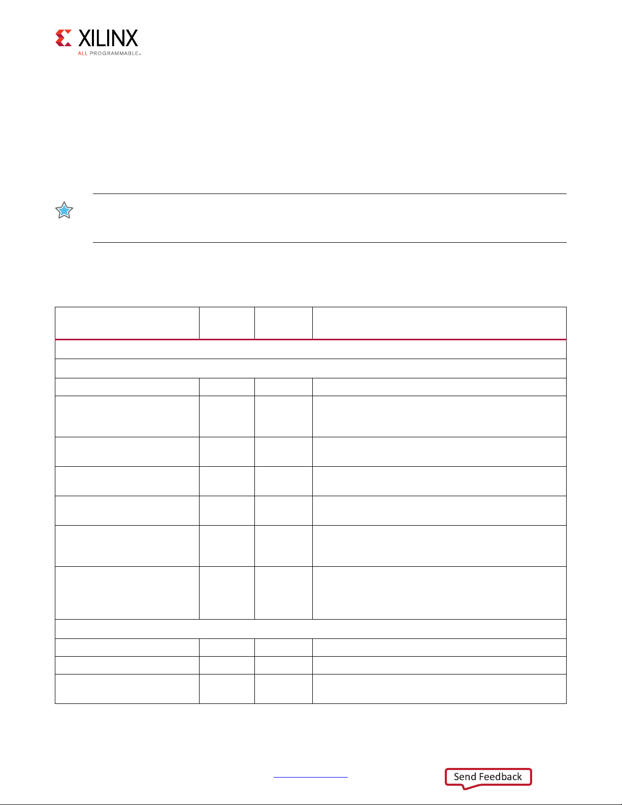
LogiCORE IP Facts
Core Specifics
Supported Device
(1)
Family
Supported User
Interfaces
Resources
Design Files Encrypted RTL
Example Design VHDL and Verilog
Test Bench
Constraints File Xilinx Design Constraints (XDC)
Simulation Model VHDL/Verilog
Supported S/W
Drivers
Design Entry Vivado® Design Suite
Simulation
Synthesis Vivado Synthesis
(2), (3)
UltraScale™ Architecture, Zynq®-7000, 7 Series
See Table 2-2, Table 2-3, Table 2-4, and
Provided with Core
Tested Design Flows
For supported simulators, see the
Xilinx Design Tools: Release Notes Guide
UltraScale+™ Families,
64-bit XG
VHDL Test Bench
Verilog Test Fixture
(4)
Devices
MII Interface
Table 2-5.
NA
Support
Provided by Xilinx, Inc.@ Xilinx Support web page
1.For a complete list of supported devices, see Vivado IP catalog. See
Verification for supported speed grades.
2.Resource utilizations for 20 G are the same as those for 10 G. For
detailed utilization numbers based upon configuration, see
Table 2-2 through Table 2-5.
3.Resource utilization depends on target device and configuration. See
Table 2-2 through Table 2-5 for detailed information.
4.For the supported versions of the tools, see the Xilinx Design Tools:
Release Notes Guide.
.
• IEEE 802.3-2012 clause 45 Management
Data Input/Output (MDIO) interface
(optional)
• IEEE 802.3-2012 clause 48 State Machines
• Available under the Xilinx End User License
Agreement
XAUI v12.3 Product Guide www.xilinx.com 5
PG053 April 6, 2016 Product Specification
Page 6

Overview
Send Feedback
XAUI is a four-lane, 3.125 Gb/s-per-lane serial interface. Each lane is a differential pair
carrying current mode logic (CML) signaling, and the data on each lane is 8B/10B encoded
before transmission. Special code groups are used to allow each lane to synchronize at a
word boundary and to deskew all four lanes into alignment at the receiving end. The XAUI
standard is fully specified in clauses 47 and 48 of the 10-Gigabit Ethernet IEEE 802.3-2012
specification.
The XAUI standard was initially developed as a means to extend the physical separation
possible between Media Access Controller (MAC) and PHY components in a 10-Gigabit
Ethernet system distributed across a circuit board and to reduce the number of interface
signals in comparison with the XGMII (10-Gigabit Ethernet Media Independent Interface).
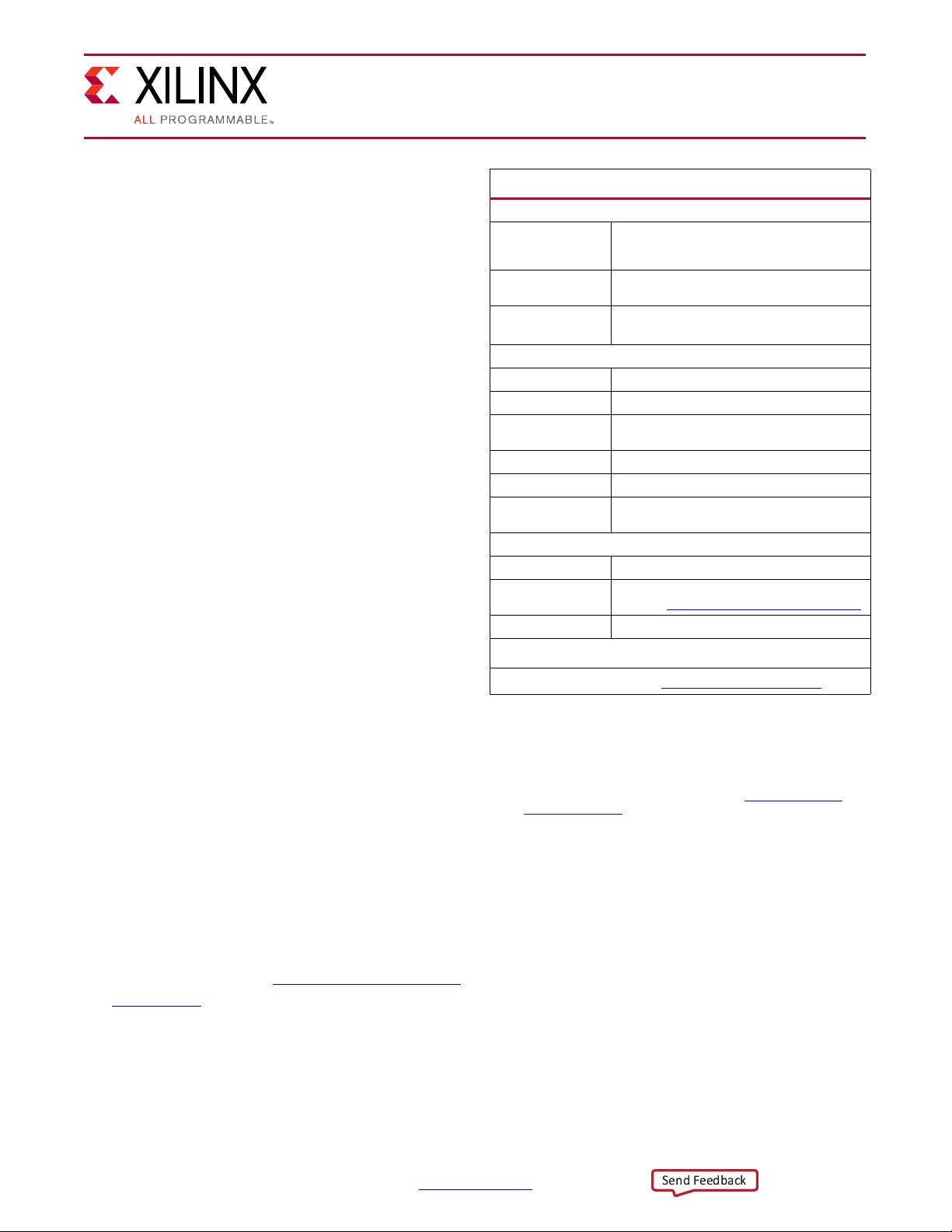
Figure 1-1 shows a block diagram of the XAUI core implementation. The major functional
blocks of the core include the following:
Chapter 1
• Transmit Idle Generation Logic creates the code groups to allow synchronization and
alignment at the receiver.
• Synchronization State Machine (one per lane) identifies byte boundaries in incoming
serial data.
• Deskew State Machine de-skews the four received lanes into alignment.
• Optional MDIO Interface is a two-wire low-speed serial interface used to manage the
core.
• Four Device-Specific Transceivers (integrated in the FPGAs) provide the high-speed
transceivers as well as 8B/10B encode and decode and elastic buffering in the receive
datapath.
XAUI v12.3 Product Guide www.xilinx.com 6
PG053 April 6, 2016
Page 7
X-Ref Target - Figure 1-1
X13667
FPGA
User Logic
Transceiver
Transceiver
Transceiver
Transceiver
Clocks and
Reset
Logic
Idle
Generation
Synchronization
Deskew
Management
Synchronization
Synchronization
Synchronization
Encrypted HDL
Core
64+8
64+8
Reference
clock
Resetclk156_out
Lane 0
Lane 1
Lane 2
Lane 3
mdc
mdio
Core
Send Feedback
Chapter 1: Overview
Figure 1‐1: Architecture of the XAUI IP Core with Client-Side User Logic
XAUI v12.3 Product Guide www.xilinx.com 7
PG053 April 6, 2016
Page 8

Chapter 1: Overview
Send Feedback
Additional Features
20-Gigabit XAUI (Double XAUI) Support
By running the XAUI interface at twice the normal clock and line rates, 20-Gigabit data rate
can be achieved. For devices and speed grades, see Speed Grades. Consult the release notes
for the core for the specific devices supported.
About the Core
The XAUI core is a Xilinx® Intellectual Property (IP) core, included in the latest IP Update on
the Xilinx IP Center. For detailed information about the core, see the XAUI product page
.
Recommended Design Experience
Although the XAUI core is a fully-verified solution, the challenge associated with
implementing a complete design varies depending on the configuration and functionality
of the application. For best results, previous experience building high performance,
pipelined Field Programmable Gate Array (FPGA) designs using Xilinx implementation
software and Xilinx Design Constraints (XDC) is recommended.
Contact your local Xilinx representative for a closer review and estimation for your specific
requirements.
XAUI v12.3 Product Guide www.xilinx.com 8
PG053 April 6, 2016
Page 9
Chapter 1: Overview
User Logic
(Ten Gigabit
Ethernet
MAC)
FPGA
XPAK Optical Module
XAUICore
low speed management signals
X13723
Send Feedback
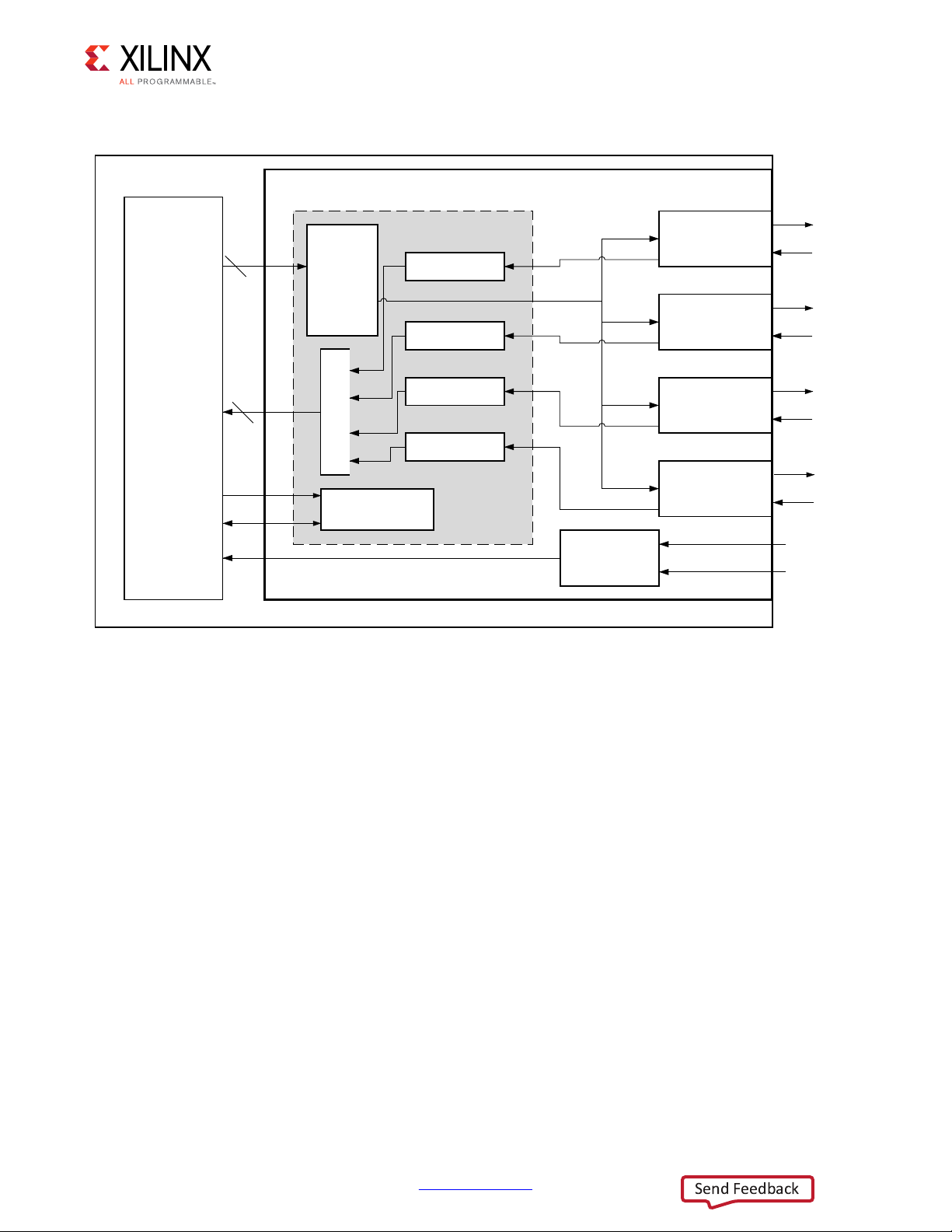
Applications
Figure 1-2 shows the XAUI core connecting a 10-Gigabit Ethernet MAC to a 10-Gigabit
XPAK optical module.
X-Ref Target - Figure 1-2
Figure 1‐2: XAUI Connecting a 10-Gigabit Ethernet MAC to an Optical Module
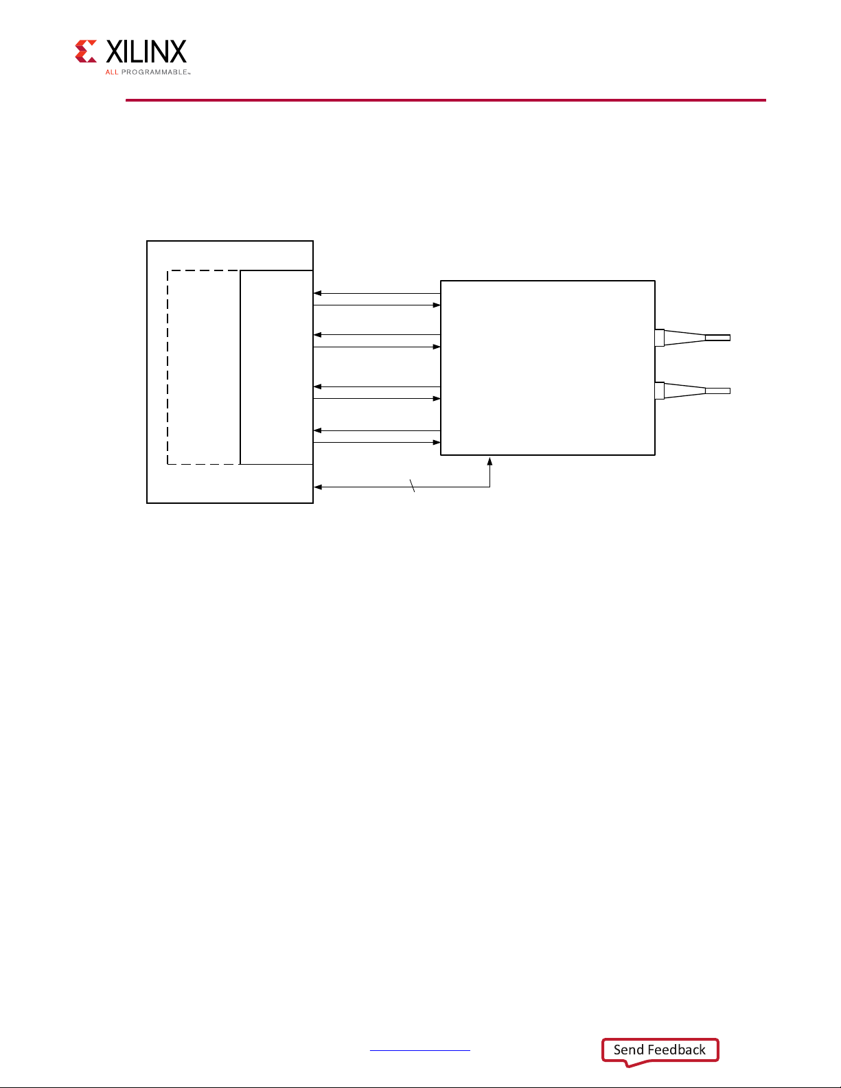
After its publication, the applications of XAUI have extended beyond 10-Gigabit Ethernet to
the backplane and other general high-speed interconnect applications. Figure 1-3 shows a
typical backplane and other general high-speed interconnect applications.
XAUI v12.3 Product Guide www.xilinx.com 9
PG053 April 6, 2016
Page 10
X-Ref Target - Figure 1-3
XAUI
Core
XAUI
Core
Up to 20in FR-4 plus 2 connectors
User
Logic
User
Logic
Backplane
FPGA FPGA
x13668
Send Feedback
Chapter 1: Overview
Figure 1‐3: Typical Backplane Application for XAUI
Licensing and Ordering Information
This Xilinx LogiCORE™ IP module is provided at no additional cost with the Xilinx Vivado®
Design Suite under the terms of the Xilinx End User License
other Xilinx LogiCORE IP modules is available at the Xilinx Intellectual Property
information about pricing and availability of other Xilinx LogiCORE IP modules and tools,
contact your local Xilinx sales representative
.
. Information about this and
page. For
XAUI v12.3 Product Guide www.xilinx.com 10
PG053 April 6, 2016
Page 11

Chapter 1: Overview
Send Feedback
Feedback
Xilinx welcomes comments and suggestions about the XAUI core and the documentation
supplied with the core.
Core
For comments or suggestions about the XAUI core, submit a webcase from Xilinx Support
web page. Be sure to include the following information:
• Product name
• Core version number
• Explanation of your comments
Document
For comments or suggestions about this document, submit a webcase from
www.xilinx.com/support
• Document title
• Document number
• Page number(s) to which your comments refer
• Explanation of your comments
. Be sure to include the following information:
XAUI v12.3 Product Guide www.xilinx.com 11
PG053 April 6, 2016
Page 12

Product Specification
Send Feedback
Standards Compliance
The XAUI IP core is designed to the standard specified in clauses 47 and 48 of the
10-Gigabit Ethernet specification IEEE Std. 802.3-2012.
Performance
This section contains the following subsections:
• Latency
Chapter 2
• Speed Grades
Latency
These measurements are for the core only; they do not include the latency through the
transceiver. The latency through the transceiver can be obtained from the relevant
transceiver user guide.
Transmit Path Latency
As measured from the input port xgmii_txd[63:0] of the transmitter side XGMII (until
that data appears on the txdata pins on the internal transceiver interface on the
transceiver interface), the latency through the core for the internal XGMII interface
configuration in the transmit direction is four clk periods of the core input usrclk.
Receive Path Latency
Measured from the input into the core encrypted hdl logic from the rxdata pins of the
internal transceiver interface until the data appears on xgmii_rxdata[63:0] of the
receiver side XGMII interface, the latency through the core in the receive direction is equal
to 4
–5 clock cycles of usrclk.
XAUI v12.3 Product Guide www.xilinx.com 12
PG053 April 6, 2016
Page 13
Chapter 2: Product Specification
Send Feedback
If the word appears on the upper half of the two-byte transceiver interface, the latency is
five clock cycles of usrclk and it appears on the lower half of the XGMII interface. If it
appears on the lower half of the two-byte interface, the latency is four clock cycles of
usrclk and it appears on the upper half of the XGMII interface.
Speed Grades
The minimum device requirements for 10G and 20G operation are listed in the following
table.
Table 2‐1: Speed Grades
Device XAUI (4x3.125G) DXAUI (4x6.25G)
UltraScale Architecture -1 -1
Zynq-7000 –1 –2
Virtex-7 –1 –2
Kintex-7 –1 –2
Artix-7 –1 –2
Resource Utilization
UltraScale Architecture Devices
Table 2-2 provides approximate resource counts for the various core options on
UltraScale™ architecture.
Table 2‐2: Device Utilization – UltraScale Architectures
Shared Logic MDIO Management LUTs FFs
In Example Design FALSE 724 995
In Example Design TRUE 864 1094
In Core FALSE 813 995
In Core TRUE 956 1094
XAUI v12.3 Product Guide www.xilinx.com 13
PG053 April 6, 2016
Page 14
Chapter 2: Product Specification
Send Feedback
Virtex-7 (GTH) FPGAs
Table 2-3 provides approximate resource counts for the various core options on Virtex®-7
FPGAs.
Table 2‐3: Device Utilization – Virtex-7 FPGAs
Shared Logic MDIO Management LUTs FFs
In Example Design FALSE 1036 1193
In Example Design TRUE 1192 1292
In Core FALSE 1114 1193
In Core TRUE 1263 1292
Zynq-7000, Virtex-7 (GTX), and Kintex-7 Devices
Table 2-4 provides approximate resource counts for the various core options Kintex-7
devices.
Note:
.
Zynq®-7000 device results are expected to be similar to Kintex-7 device results.
Table 2‐4: Device Utilization – Kintex-7 Devices
Shared Logic MDIO Management LUTs FFs
In Example Design FALSE 765 945
In Example Design TRUE 877 1044
In Core FALSE 845 945
In Core TRUE 957 1044
Artix-7 FPGAs
Table 2-5 provides approximate resource counts for the various core options on Artix®-7
FPGAs.
Table 2‐5: Device Utilization – Artix-7 FPGAs
Shared Logic MDIO Management LUTs FFs
In Example Design FALSE 1027 1186
In Example Design TRUE 1144 1285
In Core FALSE 1107 1186
XAUI v12.3 Product Guide www.xilinx.com 14
PG053 April 6, 2016
In Core TRUE 1223 1285
Page 15

Chapter 2: Product Specification
Send Feedback
Verification
The XAUI core has been verified using both simulation and hardware testing.
Simulation
A highly parameterizable transaction-based simulation test suite was used to verify the
core. Verification tests include:
• Register access over MDIO
• Loss and regain of synchronization
• Loss and regain of alignment
• Frame transmission
• Frame reception
• Clock compensation
• Recovery from error conditions
Hardware Verification
The core has been used in several hardware test platforms within Xilinx. In particular, the
®
core has been used in a test platform design with the Xilinx
design comprises the MAC, XAUI, a ping loopback First In First Out (FIFO), and a test pattern
generator all under embedded processor control. This design has been used for
conformance and interoperability testing at the University of New Hampshire
Interoperability Lab.
10-Gigabit Ethernet MAC. This
XAUI v12.3 Product Guide www.xilinx.com 15
PG053 April 6, 2016
Page 16

Chapter 2: Product Specification
Send Feedback
Port Descriptions
Client-Side Interface
The signals of the client-side interface are shown in Table 2-6. See Chapter 5, Interfacing to
the Core for more information on connecting to the client-side interface.
Table 2‐6: Client-Side Interface Ports
Signal Name Direction Clock Domain Description
xgmii_txd[63:0] IN clk156_out Transmit data, eight bytes wide
xgmii_txc[7:0] IN clk156_out Transmit control bits, one bit per transmit data byte
xgmii_rxd[63:0] OUT clk156_out Received data, eight bytes wide
xgmii_rxc[7:0] OUT clk156_out Receive control bits, one bit per received data byte
Transceiver I/O
The Transceiver Interface is no longer part of the ports of the core because it includes the
transceiver. Instead there are the following ports.
• Ports Corresponding to the I/O of the transceiver
• Dynamic Reconfiguration Port of the transceiver
See Table 2-7.
Table 2‐7: Ports Corresponding to the I/O of the Transceiver
Signal Name Direction Clock Domain Description
xaui_tx_l0_p, xaui_tx_l0_n,
xaui_tx_l1_p, xaui_tx_l1_n,
xaui_tx_l2_p, xaui_tx_l2_n,
xaui_tx_l3_p, xaui_tx_l3_n
xaui_rx_l0_p, xaui_rx_l0_n,
xaui_rx_l1_p, xaui_rx_l1_n,
xaui_rx_l2_p, xaui_rx_l2_n,
xaui_rx_l3_p, xaui_rx_l3_n
signal_detect[3:0] IN Async
OUT N/A
IN N/A
Differential complements of one another
forming a differential transmit output pair.
One pair for each of the 4 lanes.
Differential complements of one another
forming a differential receiver input pair. One
pair for each of the 4 lanes.
Intended to be driven by an attached
10GBASE-LX4 optical module; they signify
that each of the four optical receivers is
receiving illumination and is therefore not just
putting out noise. If an optical module is not
in use, this four-wire bus should be tied to
1111.
XAUI v12.3 Product Guide www.xilinx.com 16
PG053 April 6, 2016
Page 17
Transceiver Control and Status Ports
Send Feedback
Optional ports that, if enabled, allow the monitoring and control of certain important ports
of the transceivers. When not selected, these ports are tied to their default values. For
information on these ports, see the 7 Series FPGAs GTX/GTH Transceivers User Guide
(UG476) [Ref 1], the 7 Series FPGAs GTP Transceivers User Guide (UG482) [Ref 2], the
UltraScale Architecture GTH Transceivers User Guide (UG576) [Ref 3], and the Ultrascale
Architecture GTY Transceivers User Guide (UG578) [Ref 4]).
IMPORTANT: The ports in the Transceiver Control And Status Interface must be driven in accordance
with the appropriate GT user guide. Using the input signals listed in
unpredictable behavior of the IP core.
Note: The Dynamic Reconfiguration Port is only available if the Transceiver Control and Status Ports
option is selected
Table 2‐8: Transceiver Control and Status Ports —7 Series FPGAs
Chapter 2: Product Specification
Table 2-8 may result in
Signal Name Direction
Clock
Domain
Description
CHANNEL 0
GT0 DRP
gt0_drpaddr[8:0] in dclk DRP address bus for channel 0
DRP enable signal.
gt0_drpen in dclk
gt0_drpdi[15:0] in dclk
gt0_drpdo[15:0] out dclk
gt0_drprdy out dclk
gt0_drpwe in dclk
gt0_drp_busy out dclk
0: No read or write operation performed.
1: enables a read or write operation.
Data bus for writing configuration data to the
transceiver for channel 0.
Data bus for reading configuration data from the
transceiver for channel 0.
Indicates operation is complete for write operations
and data is valid for read operations for channel 0.
DRP write enable for channel 0.
0: Read operation when drpen is 1.
1: Write operation when drpen is 1.
(GTPE2 all configurations or GTHE2 10G
configuration). Indicates the DRP interface is being
used internally by the serial transceiver and should not
be driven until this signal is deasserted.
gt0_txpmareset_in in Async Starts the TX PMA reset process.
gt0_txpcsreset_in in Async Starts the TX PCS reset process.
gt0_txresetdone_out out clk156_out
XAUI v12.3 Product Guide www.xilinx.com 17
PG053 April 6, 2016
GT0 TX Reset and Initialization
When asserted the serial transceiver TX has finished
reset and is ready for use.
Page 18

Chapter 2: Product Specification
Send Feedback
Table 2‐8: Transceiver Control and Status Ports —7 Series FPGAs (Cont’d)
Signal Name Direction
Clock
Domain
Description
GT0 RX Reset and Initialization
gt0_rxpmareset_in in Async Starts the RX PMA reset process.
gt0_rxpcsreset_in in Async Starts the RX PCS reset process.
gt0_rxpmaresetdone_out out Async
gt0_rxresetdone_out out clk156_out
(GTHE2 and GTPE2) This active-High signal indicates
RX PMA reset is complete.
When asserted the serial transceiver RX has finished
reset and is ready for use.
GT0 Clocking
gt0_rxbufstatus_out[2:0] out clk156_out RX buffer status.
gt0_txphaligndone_out out Async TX phase alignment done.
gt0_txphinitdone_out out Async TX phase alignment initialization done.
gt0_txdlysresetdone_out out Async TX delay alignment soft reset done.
(GTHE2) This active-High PLL frequency lock signal
gt0_cplllock_out out Async
gt_qplllock_out out Async
indicates that the PLL frequency is within
predetermined tolerance.
(GTXE2 and GTPE2) This active-High PLL frequency lock
signal indicates that the PLL frequency is within
predetermined tolerance.
Signal Integrity and Functionality
GT0 Eye scan
gt0_eyescantrigger_in in clk156_out Causes a trigger event.
gt0_eyescanreset_in in Async
gt0_eyescandataerror_out out Async
gt0_rxrate_in[2:0] in Reserved
This port is driven High and then deasserted to start
the EYESCAN reset process.
Asserts High for one rec_clk cycle when an
(unmasked) error occurs while in the COUNT or ARMED
state.
This port dynamically controls the setting for the RX
serial clock divider.
GT0 Loopback
gt0_loopback_in[2:0] in Async Determines the loopback mode.
GT0 Polarity
gt0_rxpolarity_in in clk156_out
gt0_txpolarity_in in clk156_out
The rxpolarity port can invert the polarity of incoming
data.
The txpolarity port can invert the polarity of outgoing
data.
GT0 RX Decision Feedback Equalizer (DFE)
gt0_rxlpmen_in in Async
(GTXE2 and GTHE2) RX datapath.
0: DFE. 1: LPM.
XAUI v12.3 Product Guide www.xilinx.com 18
PG053 April 6, 2016
Page 19

Chapter 2: Product Specification
Send Feedback
Table 2‐8: Transceiver Control and Status Ports —7 Series FPGAs (Cont’d)
Signal Name Direction
gt0_rxdfelpmreset_in in Async (GTXE2 and GTHE2) Reset for LPM and DFE datapath.
gt0_rxmonitorsel_in[1:0] in Reserved
gt0_rxmonitorout_out[6:0] out Async (GTXE2 and GTHE2) Monitor output.
gt0_rxlpmreset_in in clk156_out
gt0_rxlpmhfhold_in in Async
gt0_rxlpmhfovrden_in in Async
gt0_rxlpmlfhold_in in Async
gt0_rxlpmlfovrden_in in Async
Clock
Domain
Description
(GTXE2 and GTHE2) Select signal for
gt0_rxmonitorout_out.
(GTPE2) This port is driven High and then deasserted to
start the LPM reset process.
(GTPE2) Determines whether the value of the
high-frequency boost is either held or adapted.
(GTPE2) Determines whether the high-frequency boost
is controlled by an attribute or a signal.
(GTPE2) Determines whether the value of the
low-frequency boost is either held or adapted.
(GTPE2) Determines whether the low-frequency boost
is controlled by an attribute or a signal.
GT0 TX Driver
gt0_txpostcursor_in[4:0] in Async Transmitter post-cursor TX post-emphasis control.
gt0_txprecursor_in[4:0] in Async Transmitter post-cursor TX pre-emphasis control.
gt0_txdiffctrl_in[3:0] in Async Driver Swing Control.
gt0_txinhibit_in in clk156_out When High, this signal blocks the transmission of data.
GT0 PRBS
gt0_rxprbscntreset_in in clk156_out Resets the PRBS error counter.
gt0_rxprbserr_out out clk156_out
gt0_rxprbssel_in[2:0] in clk156_out Receiver PRBS checker test pattern control.
gt0_txprbssel_in[2:0] in clk156_out Transmitter PRBS generator test pattern control.
gt0_txprbsforceerr_in in clk156_out
This non-sticky status output indicates that PRBS
errors have occurred.
When this port is driven High, errors are forced in the
PRBS transmitter. While this port is asserted, the
output data pattern contains errors.
GT0 RX CDR
gt0_rxcdrhold_in in Async Hold the CDR control loop frozen.
GT0 Digital Monitor
gt0_dmonitorout_out[7:0] out Async (GTXE2) Digital Monitor Output Bus
gt0_dmonitorout_out[14:0] out Async (GTHE2) Digital Monitor Output Bus
gt0_dmonitorout_out[14:0] out Async (GTPE2) Digital Monitor Output Bus
GT0 Status
gt0_rxdisperr_out[3:0] out clk156_out
XAUI v12.3 Product Guide www.xilinx.com 19
PG053 April 6, 2016
Active-High indicates the corresponding byte of the
received data has a disparity error
Page 20
Chapter 2: Product Specification
Send Feedback
Table 2‐8: Transceiver Control and Status Ports —7 Series FPGAs (Cont’d)
Signal Name Direction
gt0_rxnotintable_out[3:0] out clk156_out
gt0_rxcommadet_out out clk156_out
Clock
Domain
Description
Active-High indicates the corresponding byte of the
received data was not a valid character in the 8B/10B
table.
This signal is asserted when the comma alignment
block detects a comma.
CHANNEL 1
GT1 DRP
gt1_drpaddr[8:0] in dclk DRP address bus for channel 1.
DRP enable signal.
gt1_drpen in dclk
gt1_drpdi[15:0] in dclk
gt1_drpdo[15:0] out dclk
gt1_drprdy out dclk
gt1_drpwe in dclk
0: No read or write operation performed.
1: enables a read or write operation.
Data bus for writing configuration data to the
transceiver for channel 1.
Data bus for reading configuration data from the
transceiver for channel 1.
Indicates operation is complete for write operations
and data is valid for read operations for channel 1.
DRP write enable for channel 1.
0: Read operation when drpen is 1.
1: Write operation when drpen is 1.
(GTPE2 all configurations or GTHE2 10G
gt1_drp_busy out dclk
configuration). Indicates the DRP interface is being
used internally by the serial transceiver and should not
be driven until this signal is deasserted.
GT1 TX Reset and Initialization
gt1_txpmareset_in in Async Starts the TX PMA reset process.
gt1_txpcsreset_in in Async Starts the TX PCS reset process.
gt1_txresetdone_out out clk156_out
When asserted the serial transceiver TX has finished
reset and is ready for use.
GT1 RX Reset and Initialization
gt1_rxpmareset_in in Async Starts the RX PMA reset process.
gt1_rxpcsreset_in in Async Starts the RX PCS reset process.
gt1_rxpmaresetdone_out out Async
gt1_rxresetdone_out out clk156_out
(GTHE2 and GTPE2) This active-High signal indicates
RX PMA reset is complete.
When asserted the serial transceiver RX has finished
reset and is ready for use.
GT1 Clocking
gt1_rxbufstatus_out[2:0] out clk156_out RX buffer status.
gt1_txphaligndone_out out Async TX phase alignment done.
XAUI v12.3 Product Guide www.xilinx.com 20
PG053 April 6, 2016
Page 21
Chapter 2: Product Specification
Send Feedback
Table 2‐8: Transceiver Control and Status Ports —7 Series FPGAs (Cont’d)
Signal Name Direction
gt1_txphinitdone_out out Async TX phase alignment initialization done.
gt1_txdlysresetdone_out out Async TX delay alignment soft reset done.
gt1_cplllock_out out Async
Clock
Domain
Description
(GTHE2) This active-High PLL frequency lock signal
indicates that the PLL frequency is within
predetermined tolerance.
Signal Integrity and Functionality
GT1 Eye scan
gt1_eyescantrigger_in in clk156_out Causes a trigger event.
gt1_eyescanreset_in in Async
gt1_eyescandataerror_out out Async
gt1_rxrate_in[2:0] in Reserved
This port is driven High and then deasserted to start
the EYESCAN reset process.
Asserts High for one rec_clk cycle when an
(unmasked) error occurs while in the COUNT or ARMED
state.
This port dynamically controls the setting for the RX
serial clock divider.
GT1 Loopback
gt1_loopback_in[2:0] in Async Determines the loopback mode.
GT1 Polarity
gt1_rxpolarity_in in clk156_out
gt1_txpolarity_in in clk156_out
The rxpolarity port can invert the polarity of incoming
data.
The txpolarity port can invert the polarity of outgoing
data.
GT1 RX Decision Feedback Equalizer (DFE)
gt1_rxlpmen_in in Async
gt1_rxdfelpmreset_in in Async (GTXE2 and GTHE2) Reset for LPM and DFE datapath.
gt1_rxmonitorsel_in[1:0] in Reserved
gt1_rxmonitorout_out[6:0] out Async (GTXE2 and GTHE2) Monitor output.
gt1_rxlpmreset_in in clk156_out
gt1_rxlpmhfhold_in in Async
gt1_rxlpmhfovrden_in in Async
gt1_rxlpmlfhold_in in Async
(GTXE2 and GTHE2) RX datapath.
0: DFE. 1: LPM.
(GTXE2 and GTHE2) Select signal for
gt1_rxmonitorout_out.
(GTPE2) This port is driven High and then deasserted to
start the LPM reset process.
(GTPE2) Determines whether the value of the
high-frequency boost is either held or adapted.
(GTPE2) Determines whether the high-frequency boost
is controlled by an attribute or a signal.
(GTPE2) Determines whether the value of the
low-frequency boost is either held or adapted.
gt1_rxlpmlfovrden_in in Async
XAUI v12.3 Product Guide www.xilinx.com 21
PG053 April 6, 2016
(GTPE2) Determines whether the low-frequency boost
is controlled by an attribute or a signal.
Page 22

Chapter 2: Product Specification
Send Feedback
Table 2‐8: Transceiver Control and Status Ports —7 Series FPGAs (Cont’d)
Signal Name Direction
Clock
Domain
Description
GT1 TX Driver
gt1_txpostcursor_in[4:0] in Async Transmitter post-cursor TX post-emphasis control.
gt1_txprecursor_in[4:0] in Async Transmitter post-cursor TX pre-emphasis control.
gt1_txdiffctrl_in[3:0] in Async Driver Swing Control.
gt1_txinhibit_in in clk156_out When High, this signal blocks the transmission of data.
GT1 PRBS
gt1_rxprbscntreset_in in clk156_out Resets the PRBS error counter.
gt1_rxprbserr_out out clk156_out
gt1_rxprbssel_in[2:0] in clk156_out Receiver PRBS checker test pattern control.
gt1_txprbssel_in[2:0] in clk156_out Transmitter PRBS generator test pattern control.
gt1_txprbsforceerr_in in clk156_out
This non-sticky status output indicates that PRBS
errors have occurred.
When this port is driven High, errors are forced in the
PRBS transmitter. While this port is asserted, the
output data pattern contains errors.
GT1 RX CDR
gt1_rxcdrhold_in in Async Hold the CDR control loop frozen.
GT1 Digital Monitor
gt1_dmonitorout_out[7:0] out Async (GTXE2) Digital Monitor Output Bus
gt1_dmonitorout_out[14:0] out Async (GTHE2) Digital Monitor Output Bus
gt1_dmonitorout_out[14:0] out Async (GTPE2) Digital Monitor Output Bus
GT1 Status
gt1_rxdisperr_out[3:0] out clk156_out
gt1_rxnotintable_out[3:0] out clk156_out
gt1_rxcommadet_out out clk156_out
Active-High indicates the corresponding byte of the
received data has a disparity error
Active-High indicates the corresponding byte of the
received data was not a valid character in the 8B/10B
table.
This signal is asserted when the comma alignment
block detects a comma.
CHANNEL 2
GT2 DRP
gt2_drpaddr[8:0] in dclk DRP address bus for channel 2.
DRP enable signal.
gt2_drpen in dclk
gt2_drpdi[15:0] in dclk
0: No read or write operation performed.
1: enables a read or write operation.
Data bus for writing configuration data to the
transceiver for channel 2.
XAUI v12.3 Product Guide www.xilinx.com 22
PG053 April 6, 2016
Page 23

Chapter 2: Product Specification
Send Feedback
Table 2‐8: Transceiver Control and Status Ports —7 Series FPGAs (Cont’d)
Signal Name Direction
gt2_drpdo[15:0] out dclk
gt2_drprdy out dclk
gt2_drpwe in dclk
gt2_drp_busy out dclk
Clock
Domain
Description
Data bus for reading configuration data from the
transceiver for channel 2.
Indicates operation is complete for write operations
and data is valid for read operations for channel 2.
DRP write enable for channel 2.
0: Read operation when drpen is 1.
1: Write operation when drpen is 1.
(GTPE2 all configurations or GTHE2 10G
configuration). Indicates the DRP interface is being
used internally by the serial transceiver and should not
be driven until this signal is deasserted.
GT2 TX Reset and Initialization
gt2_txpmareset_in in Async Starts the TX PMA reset process.
gt2_txpcsreset_in in Async Starts the TX PCS reset process.
gt2_txresetdone_out out clk156_out
When asserted the serial transceiver TX has finished
reset and is ready for use.
GT2 RX Reset and Initialization
gt2_rxpmareset_in in Async Starts the RX PMA reset process.
gt2_rxpcsreset_in in Async Starts the RX PCS reset process.
gt2_rxpmaresetdone_out out Async
gt2_rxresetdone_out out clk156_out
(GTHE2 and GTPE2) This active-High signal indicates
RX PMA reset is complete.
When asserted the serial transceiver RX has finished
reset and is ready for use.
GT2 Clocking
gt2_rxbufstatus_out[2:0] out clk156_out RX buffer status.
gt2_txphaligndone_out out Async TX phase alignment done.
gt2_txphinitdone_out out Async TX phase alignment initialization done.
gt2_txdlysresetdone_out out Async TX delay alignment soft reset done.
(GTHE2) This active-High PLL frequency lock signal
gt2_cplllock_out out Async
indicates that the PLL frequency is within
predetermined tolerance.
Signal Integrity and Functionality
GT2 Eye Scan
gt2_eyescantrigger_in in clk156_out Causes a trigger event.
gt2_eyescanreset_in in Async
gt2_eyescandataerror_out out Async
This port is driven High and then deasserted to start
the EYESCAN reset process.
Asserts High for one rec_clk cycle when an (unmasked)
error occurs while in the COUNT or ARMED state.
XAUI v12.3 Product Guide www.xilinx.com 23
PG053 April 6, 2016
Page 24
Chapter 2: Product Specification
Send Feedback
Table 2‐8: Transceiver Control and Status Ports —7 Series FPGAs (Cont’d)
Signal Name Direction
gt2_rxrate_in[2:0] in Reserved
Clock
Domain
Description
This port dynamically controls the setting for the RX
serial clock divider.
GT2 Loopback
gt2_loopback_in[2:0] in Async Determines the loopback mode.
GT2 Polarity
gt2_rxpolarity_in in clk156_out
gt2_txpolarity_in in clk156_out
The rxpolarity port can invert the polarity of incoming
data.
The txpolarity port can invert the polarity of outgoing
data.
GT2 RX Decision Feedback Equalizer (DFE)
(GTXE2 and GTHE2) RX datapath.
gt2_rxlpmen_in in Async
gt2_rxdfelpmreset_in in Async (GTXE2 and GTHE2) Reset for LPM and DFE datapath.
gt2_rxmonitorsel_in[1:0] in Reserved
gt2_rxmonitorout_out[6:0] out Async (GTXE2 and GTHE2) Monitor output.
0: DFE.
1: LPM.
(GTXE2 and GTHE2) Select signal for
gt2_rxmonitorout_out.
gt2_rxlpmreset_in in clk156_out
gt2_rxlpmhfhold_in in Async
gt2_rxlpmhfovrden_in in Async
gt2_rxlpmlfhold_in in Async
gt2_rxlpmlfovrden_in in Async
(GTPE2) This port is driven High and then deasserted to
start the LPM reset process.
(GTPE2) Determines whether the value of the
high-frequency boost is either held or adapted.
(GTPE2) Determines whether the high-frequency boost
is controlled by an attribute or a signal.
(GTPE2) Determines whether the value of the
low-frequency boost is either held or adapted.
(GTPE2) Determines whether the low-frequency boost
is controlled by an attribute or a signal.
GT2 TX Driver
gt2_txpostcursor_in[4:0] in Async Transmitter post-cursor TX post-emphasis control.
gt2_txprecursor_in[4:0] in Async Transmitter post-cursor TX pre-emphasis control.
gt2_txdiffctrl_in[3:0] in Async Driver Swing Control.
gt2_txinhibit_in in clk156_out When High, this signal blocks the transmission of data.
GT2 PRBS
gt2_rxprbscntreset_in in clk156_out Resets the PRBS error counter.
gt2_rxprbserr_out out clk156_out
This non-sticky status output indicates that PRBS
errors have occurred.
gt2_rxprbssel_in[2:0] in clk156_out Receiver PRBS checker test pattern control.
XAUI v12.3 Product Guide www.xilinx.com 24
PG053 April 6, 2016
Page 25
Chapter 2: Product Specification
Send Feedback
Table 2‐8: Transceiver Control and Status Ports —7 Series FPGAs (Cont’d)
Signal Name Direction
gt2_txprbssel_in[2:0] in clk156_out Transmitter PRBS generator test pattern control.
gt2_txprbsforceerr_in in clk156_out
Clock
Domain
Description
When this port is driven High, errors are forced in the
PRBS transmitter. While this port is asserted, the
output data pattern contains errors.
GT2 RX CDR
gt2_rxcdrhold_in in Async Hold the CDR control loop frozen.
GT2 Digital Monitor
gt2_dmonitorout_out[7:0] out Async (GTXE2) Digital Monitor Output Bus
gt2_dmonitorout_out[14:0] out Async (GTHE2) Digital Monitor Output Bus
gt2_dmonitorout_out[14:0] out Async (GTPE2) Digital Monitor Output Bus
GT2 Status
gt2_rxdisperr_out[3:0] out clk156_out
gt2_rxnotintable_out[3:0] out clk156_out
gt2_rxcommadet_out out clk156_out
Active-High indicates the corresponding byte of the
received data has a disparity error
Active-High indicates the corresponding byte of the
received data was not a valid character in the 8B/10B
table.
This signal is asserted when the comma alignment
block detects a comma.
CHANNEL 3
GT3 DRP
gt3_drpaddr[8:0] in dclk DRP address bus for channel 3.
DRP enable signal.
gt3_drpen in dclk
gt3_drpdi[15:0] in dclk
gt3_drpdo[15:0] out dclk
gt3_drprdy out dclk
gt3_drpwe in dclk
gt3_drp_busy out dclk
0: No read or write operation performed.
1: enables a read or write operation.
Data bus for writing configuration data to the
transceiver for channel 3.
Data bus for reading configuration data from the
transceiver for channel 3.
Indicates operation is complete for write operations
and data is valid for read operations for channel 3.
DRP write enable for channel 3.
0: Read operation when drpen is 1.
1: Write operation when drpen is 1.
(GTPE2 all configurations or GTHE2 10G
configuration). Indicates the DRP interface is being
used internally by the serial transceiver and should not
be driven until this signal is deasserted.
XAUI v12.3 Product Guide www.xilinx.com 25
PG053 April 6, 2016
Page 26

Chapter 2: Product Specification
Send Feedback
Table 2‐8: Transceiver Control and Status Ports —7 Series FPGAs (Cont’d)
Signal Name Direction
Clock
Domain
Description
GT3 TX Reset and Initialization
gt3_txpmareset_in in Async Starts the TX PMA reset process.
gt3_txpcsreset_in in Async Starts the TX PCS reset process.
gt3_txresetdone_out out clk156_out
When asserted the serial transceiver TX has finished
reset and is ready for use.
GT3 RX Reset and Initialization
gt3_rxpmareset_in in Async Starts the RX PMA reset process.
gt3_rxpcsreset_in in Async Starts the RX PCS reset process.
gt3_rxpmaresetdone_out out Async
gt3_rxresetdone_out out clk156_out
(GTHE2 and GTPE2) This active-High signal indicates
RX PMA reset is complete.
When asserted the serial transceiver RX has finished
reset and is ready for use.
GT3 Clocking
gt3_rxbufstatus_out[2:0] out clk156_out RX buffer status.
gt3_txphaligndone_out out Async TX phase alignment done.
gt3_txphinitdone_out out Async TX phase alignment initialization done.
gt3_txdlysresetdone_out out Async TX delay alignment soft reset done.
(GTHE2) This active-High PLL frequency lock signal
gt3_cplllock_out out Async
indicates that the PLL frequency is within
predetermined tolerance.
Signal Integrity and Functionality
GT3 Eye Scan
gt3_eyescantrigger_in in clk156_out Causes a trigger event.
gt3_eyescanreset_in in Async
gt3_eyescandataerror_out out Async
gt3_rxrate_in[2:0] in Reserved
This port is driven High and then deasserted to start
the EYESCAN reset process.
Asserts High for one rec_clk cycle when an (unmasked)
error occurs while in the COUNT or ARMED state.
This port dynamically controls the setting for the RX
serial clock divider.
GT3 Loopback
gt3_loopback_in[2:0] in Async Determines the loopback mode.
GT3 Polarity
gt3_rxpolarity_in in clk156_out
gt3_txpolarity_in in clk156_out
The rxpolarity port can invert the polarity of incoming
data.
The txpolarity port can invert the polarity of outgoing
data.
XAUI v12.3 Product Guide www.xilinx.com 26
PG053 April 6, 2016
Page 27

Chapter 2: Product Specification
Send Feedback
Table 2‐8: Transceiver Control and Status Ports —7 Series FPGAs (Cont’d)
Signal Name Direction
Clock
Domain
Description
GT3 RX Decision Feedback Equalizer (DFE)
gt3_rxlpmen_in in Async
gt3_rxdfelpmreset_in in Async (GTXE2 and GTHE2) Reset for LPM and DFE datapath.
gt3_rxmonitorsel_in[1:0] in Reserved
gt3_rxmonitorout_out[6:0] out Async (GTXE2 and GTHE2) Monitor output.
gt3_rxlpmreset_in in clk156_out
gt3_rxlpmhfhold_in in Async
gt3_rxlpmhfovrden_in in Async
gt3_rxlpmlfhold_in in Async
gt3_rxlpmlfovrden_in in Async
(GTXE2 and GTHE2) RX datapath.
0: DFE. 1: LPM.
(GTXE2 and GTHE2) Select signal for
gt3_rxmonitorout_out.
(GTPE2) This port is driven High and then deasserted to
start the LPM reset process.
(GTPE2) Determines whether the value of the
high-frequency boost is either held or adapted.
(GTPE2) Determines whether the high-frequency boost
is controlled by an attribute or a signal.
(GTPE2) Determines whether the value of the
low-frequency boost is either held or adapted.
(GTPE2) Determines whether the low-frequency boost
is controlled by an attribute or a signal.
GT3 TX Driver
gt3_txpostcursor_in[4:0] in Async Transmitter post-cursor TX post-emphasis control.
gt3_txprecursor_in[4:0] in Async Transmitter post-cursor TX pre-emphasis control.
gt3_txdiffctrl_in[3:0] in Async Driver Swing Control.
gt3_txinhibit_in in clk156_out When High, this signal blocks the transmission of data.
GT3 PRBS
gt3_rxprbscntreset_in in clk156_out Resets the PRBS error counter.
gt3_rxprbserr_out out clk156_out
gt3_rxprbssel_in[2:0] in clk156_out Receiver PRBS checker test pattern control.
gt3_txprbssel_in[2:0] in clk156_out Transmitter PRBS generator test pattern control.
gt3_txprbsforceerr_in in clk156_out
This non-sticky status output indicates that PRBS
errors have occurred.
When this port is driven High, errors are forced in the
PRBS transmitter. While this port is asserted, the
output data pattern contains errors.
GT3 RX CDR
gt3_rxcdrhold_in in Async Hold the CDR control loop frozen.
GT3 Digital Monitor
gt3_dmonitorout_out[7:0] out Async (GTXE2) Digital Monitor Output Bus
gt3_dmonitorout_out[14:0] out Async (GTHE2) Digital Monitor Output Bus
gt3_dmonitorout_out[14:0] out Async (GTPE2) Digital Monitor Output Bus
XAUI v12.3 Product Guide www.xilinx.com 27
PG053 April 6, 2016
Page 28
Chapter 2: Product Specification
Send Feedback
Table 2‐8: Transceiver Control and Status Ports —7 Series FPGAs (Cont’d)
Signal Name Direction
Clock
Domain
Description
GT3 Status
gt3_rxdisperr_out[3:0] out clk156_out
gt3_rxnotintable_out[3:0] out clk156_out
gt3_rxcommadet_out out clk156_out
Active-High indicates the corresponding byte of the
received data has a disparity error
Active-High indicates the corresponding byte of the
received data was not a valid character in the 8B/10B
table.
This signal is asserted when the comma alignment
block detects a comma.
Table 2‐9: Transceiver Control and Status Ports — UltraScale Architectures
Signal Name Direction
Clock
Domain
Description
GT0 DRP
gt0_drpaddr[8:0] in dclk DRP address bus for channel 0
DRP enable signal.
gt0_drpen in dclk
gt0_drpdi[15:0] in dclk
0: No read or write operation performed.
1: enables a read or write operation.
Data bus for writing configuration data to the transceiver
for channel 0.
gt0_drpdo[15:0] out dclk
gt0_drprdy out dclk
gt0_drpwe in dclk
Data bus for reading configuration data from the
transceiver for channel 0.
Indicates operation is complete for write operations and
data is valid for read operations for channel 0.
DRP write enable for channel 0.
0: Read operation when drpen is 1.
1: Write operation when drpen is 1.
GT1 DRP
gt1_drpaddr[8:0] in dclk DRP address bus for channel 1
DRP enable signal.
gt1_drpen in dclk
gt1_drpdi[15:0] in dclk
gt1_drpdo[15:0] out dclk
gt1_drprdy out dclk
0: No read or write operation performed.
1: enables a read or write operation.
Data bus for writing configuration data to the transceiver
for channel 1.
Data bus for reading configuration data from the
transceiver for channel 1.
Indicates operation is complete for write operations and
data is valid for read operations for channel 1.
XAUI v12.3 Product Guide www.xilinx.com 28
PG053 April 6, 2016
Page 29

Chapter 2: Product Specification
Send Feedback
Table 2‐9: Transceiver Control and Status Ports — UltraScale Architectures (Cont’d)
Signal Name Direction
gt1_drpwe in dclk
Clock
Domain
Description
DRP write enable for channel 1.
0: Read operation when drpen is 1.
1: Write operation when drpen is 1.
GT2 DRP
gt2_drpaddr[8:0] in dclk DRP address bus for channel 2
DRP enable signal.
gt2_drpen in dclk
gt2_drpdi[15:0] in dclk
gt2_drpdo[15:0] out dclk
gt2_drprdy out dclk
gt2_drpwe in dclk
0: No read or write operation performed.
1: enables a read or write operation.
Data bus for writing configuration data to the transceiver
for channel 2.
Data bus for reading configuration data from the
transceiver for channel 2.
Indicates operation is complete for write operations and
data is valid for read operations for channel 2.
DRP write enable for channel 2.
0: Read operation when drpen is 1.
1: Write operation when drpen is 1.
GT3 DRP
gt3_drpaddr[8:0] in dclk DRP address bus for channel 3
DRP enable signal.
gt3_drpen in dclk
gt3_drpdi[15:0] in dclk
gt3_drpdo[15:0] out dclk
gt3_drprdy out dclk
gt3_drpwe in dclk
0: No read or write operation performed.
1: enables a read or write operation.
Data bus for writing configuration data to the transceiver
for channel 3.
Data bus for reading configuration data from the
transceiver for channel 3.
Indicates operation is complete for write operations and
data is valid for read operations for channel 3.
DRP write enable for channel 3.
0: Read operation when drpen is 1.
1: Write operation when drpen is 1.
DRP Reset
Bits 2, 18, 34 and 50 are connected to port pcsrsvdin[2] of
gt_pcsrsvdin[63:0] in Async
GT lanes 0, 1, 2 and 3 respectively. See the appropriate
transceiver user guide for more details.
TX Reset and Initialization
gt_txpmareset[3:0] in Async Starts the TX PMA reset process.
gt_txpcsreset[3:0] in Async Starts the TX PCS reset process.
XAUI v12.3 Product Guide www.xilinx.com 29
PG053 April 6, 2016
Page 30
Chapter 2: Product Specification
Send Feedback
Table 2‐9: Transceiver Control and Status Ports — UltraScale Architectures (Cont’d)
Signal Name Direction
gt_txresetdone[3:0] out clk156_out
Clock
Domain
Description
When asserted the serial transceiver TX has finished reset
and is ready for use.
RX Reset and Initialization
gt_rxpmareset[3:0] in Async Starts the RX PMA reset process.
gt_rxpcsreset[3:0] in Async Starts the RX PCS reset process.
gt_rxpmaresetdone[3:0] out Async
gt_rxresetdone[3:0] out clk156_out
When asserted the serial transceiver RX has finished reset
and is ready for use.
Clocking
gt_rxbufstatus[11:0] out clk156_out RX buffer status.
gt_txphaligndone[3:0] out Async TX phase alignment done.
gt_txphinitdone[3:0] out Async TX phase alignment initialization done.
gt_txdlysresetdone[3:0] out Async TX delay alignment soft reset done.
gt_qplllock out Async
This active-High PLL frequency lock signal indicates that the
PLL frequency is within predetermined tolerance.
Signal Integrity and Functionality
Eye Scan
gt_eyescantrigger[3:0] in clk156_out Causes a trigger event.
gt_eyescanreset[3:0] in Async
gt_eyescandataerror[3:0] out Async
gt_rxrate[11:0] in clk156_out
This port is driven High and then deasserted to start the
EYESCAN reset process.
Asserts High for one rec_clk cycle when an (unmasked) error
occurs while in the COUNT or ARMED state.
This port dynamically controls the setting for the RX serial
clock divider.
Loopback
gt_loopback[11:0] in Async Determines the loopback mode.
Polarity
gt_rxpolarity[3:0] in clk156_out The rxpolarity port can invert the polarity of incoming data.
gt_txpolarity[3:0] in clk156_out The txpolarity port can invert the polarity of outgoing data.
RX Decision Feedback Equalizer (DFE)
RX datapath.
gt_rxlpmen[3:0] in Async
gt_rxdfelpmreset[3:0] in Async Reset for LPM and DFE datapath.
0: DFE.
1: LPM.
gt_txpostcursor[19:0] in Async Transmitter post-cursor TX post-emphasis control.
XAUI v12.3 Product Guide www.xilinx.com 30
PG053 April 6, 2016
TX Driver
Page 31

Chapter 2: Product Specification
Send Feedback
Table 2‐9: Transceiver Control and Status Ports — UltraScale Architectures (Cont’d)
Signal Name Direction
gt_txprecursor[19:0] in Async Transmitter post-cursor TX pre-emphasis control.
gt_txdiffctrl[19:0 or 15:0] in Async
gt_txinhibit3:0] in clk156_out When High, this signal blocks the transmission of data.
Clock
Domain
Description
Driver Swing Control. The bus size is 20 bits for GTYE3 and
16 bits for GTHE3.
PRBS
gt_rxprbscntreset[3:0] in clk156_out Resets the PRBS error counter.
gt_rxprbserr[3:0] out clk156_out
gt_rxprbssel[15:0] in clk156_out Receiver PRBS checker test pattern control.
gt_txprbssel[15:0] in clk156_out Transmitter PRBS generator test pattern control.
gt_txprbsforceerr[3:0] in clk156_out
This non-sticky status output indicates that PRBS errors
have occurred.
When this port is driven High, errors are forced in the PRBS
transmitter. While this port is asserted, the output data
pattern contains errors.
RX CDR
gt_rxcdrhold[3:0] in Async Hold the CDR control loop frozen.
Digital Monitor
gt_dmonitorout[67:0] out Async Digital Monitor Output Bus
Status
gt_rxdisperr[7:0] out clk156_out
gt_rxnotintable[7:0] out clk156_out
gt_rxcommadet[3:0] out clk156_out
If you are migrating from a 7 series to an UltraScale device, the prefixes of the optional transceiver debug ports for
single-lane cores are changed from “gt0”, “gt1” to “gt”, and the suffix “_in” and “_out” are dropped. For multi-lane
cores, the prefixes of the optional transceiver debug ports gt(n) are aggregated into a single port. See Device Migration
for more information.
Active-High indicates the corresponding byte of the
received data has a disparity error.
Active-High indicates the corresponding byte of the
received data was not a valid character in the 8B/10B table.
This signal is asserted when the comma alignment block
detects a comma.
MDIO Interface
The MDIO Interface signals are shown in Table 2-10. More information on using this
interface can be found in Chapter 5, Interfacing to the Core.
Table 2‐10: MDIO Management Interface Ports
Signal Name Direction
Clock
Domain
Description
mdc in Async Management clock
mdio_in in Async MDIO input
XAUI v12.3 Product Guide www.xilinx.com 31
PG053 April 6, 2016
Page 32

Table 2‐10: MDIO Management Interface Ports (Cont’d)
Send Feedback
Chapter 2: Product Specification
Signal Name Direction
mdio_out out clk156_out MDIO output
mdio_tri out clk156_out
type_sel[1:0] in Tie-off Type select
prtad[4:0] in Tie-off
Clock
Domain
Description
MDIO 3-state; ‘1’ disconnects the output driver from the MDIO
bus.
MDIO port address; you should set this to provide a unique ID
on the MDIO bus.
Configuration and Status Signals
The Configuration and Status Signals are shown in Table 2-11. See Configuration and Status
Interfaces for more information on these signals, including a breakdown of the
configuration and status vectors.
Table 2‐11: Configuration and Status Ports
Signal Name Direction
configuration_ vector[6:0] in clk156_out Configuration information for the core.
status_vector[7:0] out clk156_out Status information from the core.
Clock
Domain
Description
debug[5] out clk156_out
debug[4:1] out clk156_out
debug[0] out clk156_out
align_status: 1 when the XAUI receiver is
aligned across all four lanes, 0 otherwise.
sync_status: Each pin is 1 when the respective
XAUI lane receiver is synchronized to byte
boundaries, 0 otherwise.
Indicates when the TX phase alignment of the
transceiver has been completed.
Clocking and Reset Signals and Module
Included in the example design top-level sources are circuits for clock and reset
management. These can include Digital Clock Managers (DCMs), Mixed-Mode Clock
Managers (MMCMs), reset synchronizers, or other useful utility circuits that might be useful
in your particular application.
XAUI v12.3 Product Guide www.xilinx.com 32
PG053 April 6, 2016
Page 33

Chapter 2: Product Specification
Send Feedback
Table 2-12 shows the ports that are associated with system clocks and resets.
Table 2‐12: Clock and Reset Ports with Shared Logic in the Example Design
Signal Name Direction Description
Clock used as the DRP clock, and also as a stable reference clock for the
detection of the feedback and reference clock signals to the QPLL. The
dclk in
input reference clock to the QPLL or any output clock generated from
the QPLL (for example, TXOUTCLK) must not be used to drive this clock.
For UltraScale devices, this clock is also used in the internal state
machines for the configuration of the transceiver.
refclk_p/refclk_n in
refclk in
clk156_out out
clk156_lock out
reset in Asynchronous external reset
Transceiver differential reference clock to the core when shared logic is
included in the core.
Transceiver reference clock to the core when shared logic is included in
the example design.
System clock for the encrypted HDL logic and for the device-specific
transceiver logic ports. This clock must have a frequency of 156.25 MHz
for 10G XAUI operation. 312.5 MHz for 20G XAUI operation.
This active-High PLL frequency lock signal indicates that the PLL
frequency is within predetermined tolerance. The transceiver and its
clock outputs are not reliable until this condition is met.
Table 2-13 shows the ports that are associated with system clocks and resets.
Table 2‐13: Clock and Reset Ports with Shared Logic in Core
Signal Name Direction Description
Clock used as the DRP clock, and also as a stable reference clock for the
detection of the feedback and reference clock signals to the QPLL. The
dclk in
input reference clock to the QPLL or any output clock generated from
the QPLL (for example, TXOUTCLK) must not be used to drive this clock.
For UltraScale devices this clock is also used in the internal state
machines for the configuration of the transceiver.
XAUI v12.3 Product Guide www.xilinx.com 33
PG053 April 6, 2016
refclk_p in Differential transceiver reference clock “p.”
refclk_n in Differential transceiver reference clock “n.”
System clock for the encrypted HDL logic and for the device-specific
clk156_out out
clk156_lock out
reset in Asynchronous external reset
transceiver logic ports. This clock must have a frequency of 156.25 MHz
for 10G XAUI operation. 312.5 MHz for 20G XAUI operation.
This active-High PLL frequency lock signal indicates that the PLL
frequency is within predetermined tolerance. The transceiver and its
clock outputs are not reliable until this condition is met.
Page 34

Chapter 2: Product Specification
Send Feedback
Register Space
MDIO Management Registers
The XAUI core, when generated with an MDIO interface, implements an MDIO Interface
Register block. The core responds to MDIO transactions as either a 10GBASE-X PCS, a DTE
XS, or a PHY XS depending on the setting of the type_sel port (see Table 2-10).
10GBASE-X PCS/PMA Register Map
When the core is configured as a 10GBASE-X Physical Coding Sublayer/Physical Medium
Attachment (PCS/PMA), it occupies MDIO Device Addresses 1 and 3 in the MDIO register
address map, as shown in Table 2-14.
Table 2‐14: 10GBASE-X PCS/PMA MDIO Registers
Register Address Register Name
1.0
1.1 PMA/PMD Status 1
1.2,1.3 PMA/PMD Device Identifier
1.4 PMA/PMD Speed Ability
1.5, 1.6 PMA/PMD Devices in Package
1.7 10G PMA/PMD Control 2
1.8 10G PMA/PMD Status 2
1.9 Reserved
1.10 10G PMD Receive Signal OK
1.11 TO 1.13 Reserved
1.14, 1.15 PMA/PMD Package Identifier
1.16 to 1.65 535 Reserved
3.0 PCS Control 1
3.1 PCS Status 1
3.2, 3.3 PCS Device Identifier
3.4 PCS Speed Ability
Physical Medium Attachment/Physical Medium Dependent (PMA/PMD)
Control 1
XAUI v12.3 Product Guide www.xilinx.com 34
PG053 April 6, 2016
3.5, 3.6 PCS Devices in Package
3.7 10G PCS Control 2
3.8 10G PCS Status 2
3.9 to 3.13 Reserved
3.14, 3.15 Package Identifier
Page 35

Table 2‐14: 10GBASE-X PCS/PMA MDIO Registers (Cont’d)
RESET
RSVD
RSVD
RSVD
RSVD
POWER DOWN
LOOPBACK
SPEED
SPEED
SPEED
15 14 13 12 11 10 7 6 5 2 1 0
Reg 1.0
X13682
Send Feedback
Register Address Register Name
3.16 to 3.23 Reserved
3.24 10GBASE-X PCS Status
3.25 10GBASE-X Test Control
3.26 to 3.65 535 Reserved
MDIO Register 1.0: PMA/PMD Control 1
Figure 2-1 shows the MDIO Register 1.0: PMA/PMD Control 1.
X-Ref Target - Figure 2-1
Chapter 2: Product Specification
Figure 2‐1: PMA/PMD Control 1 Register
Table 2-15 shows the PMA Control 1 register bit definitions.
Table 2‐15: PMA/PMD Control 1 Register Bit Definitions
Bit Name Description Attributes
1 = Block reset
0 = Normal operation
1.0.15 Reset
1.0.14 Reserved
1.0.13
Speed
Selection
1.0.12 Reserved
1.0.11
Power
down
The XAUI block is reset when this bit is set to 1. It
returns to 0 when the reset is complete. The
soft_reset pin is connected to this bit. This can be
connected to the reset of any other MMDs.
The block always returns 0 for this bit and ignores
writes.
The block always returns 1 for this bit and ignores
writes.
The block always returns 0 for this bit and ignores
writes.
1 = Power down mode
0 = Normal operation
When set to 1, the serial transceivers are placed in
a low-power state. Set to 0 to return to normal
operation
R/W
Self-clearing
R/O 0
R/O 1
R/O 0
R/W 0
Default
Value
0
The block always returns 0 for these bits and
ignores writes.
R/O All 0s
1.0.10:7 Reserved
XAUI v12.3 Product Guide www.xilinx.com 35
PG053 April 6, 2016
Page 36

Table 2‐15: PMA/PMD Control 1 Register Bit Definitions (Cont’d)
RSVD
RSVD
RSVD
LOCAL FAULT
POWERDOWN ABILITY
RX LINK STATUS
15 876 3210
Reg 1.1
X13683
Send Feedback
Chapter 2: Product Specification
Bit Name Description Attributes
1.0.6
1.0.5:2
Speed
Selection
Speed
Selection
1.0.1 Reserved
1.0.0 Loopback
The block always returns 1 for this bit and ignores
writes.
The block always returns 0s for these bits and
ignores writes.
The block always returns 0 for this bit and ignores
writes.
1 = Enable loopback mode
0 = Disable loopback mode
The XAUI block loops the signal in the serial
transceivers back into the receiver.
R/O 1
R/O All 0s
R/O All 0s
R/W 0
MDIO Register 1.1: PMA/PMD Status 1
Figure 2-2 shows the MDIO Register 1.1: PMA/PMD Status 1.
X-Ref Target - Figure 2-2
Default
Value
Table 2-16 shows the PMA/PMD Status 1 register bit definitions.
Table 2‐16: PMA/PMD Status 1 Register Bit Definitions
Bit Name Description Attributes
1.1.15:8 Reserved The block always returns 0 for this bit. R/O 0
1.1.7 Local Fault The block always returns 0 for this bit. R/O 0
1.1.6:3 Reserved The block always returns 0 for this bit. R/O 0
1.1.2
1.1.1
1.1.0 Reserved The block always returns 0 for this bit. R/O 0
Receive Link
Status
Power Down
Ability
Figure 2‐2: PMA/PMD Status 1 Register
The block always returns 1 for this bit. R/O 1
The block always returns 1 for this bit. R/O 1
Default
Val ue
XAUI v12.3 Product Guide www.xilinx.com 36
PG053 April 6, 2016
Page 37

Chapter 2: Product Specification
PMA/PMD
IDENTIFIER
15 0
Reg 1.2
PMA/PMD
IDENTIFIER
15
0
Reg 1.3
X13684
RSVD
10G CAPABLE
15 0
Reg 1.4
X13685
Send Feedback
MDIO Registers 1.2 and 1.3: PMA/PMD Device Identifier
Figure 2-3 shows the MDIO Registers 1.2 and 1.3: PMA/PMD Device Identifier.
X-Ref Target - Figure 2-3
Figure 2‐3: PMA/PMD Device Identifier Registers
Table 2-17 shows the PMA/PMD Device Identifier registers bit definitions.
Table 2‐17: PMA/PMD Device Identifier Registers Bit Definitions
Bit Name Description Attributes
1.2.15:0
1.3.15:0
PMA/PMD
Identifier
PMA/PMD
Identifier
The block always returns 0 for these bits and
ignores writes.
The block always returns 0 for these bits and
ignores writes.
R/O All 0s
R/O All 0s
MDIO Register 1.4: PMA/PMD Speed Ability
Figure 2-4 shows the MDIO Register 1.4: PMA/PMD Speed Ability.
X-Ref Target - Figure 2-4
Figure 2‐4: PMA/PMD Speed Ability Register
Default
Val ue
XAUI v12.3 Product Guide www.xilinx.com 37
PG053 April 6, 2016
Page 38

Chapter 2: Product Specification
VENDOR2 PRESENT
VENDOR1 PRESENT
RSVD
15 14 13 0
Reg 1.6
RSVD
DTE XS PRESENT
PHY XS PRESENT
PCS PRESENT
WIS PRESENT
PMD/PMA PRESENT
CLAUSE 22 PRESENT
15
01
23456
Reg 1.5
X13686
Send Feedback
Table 2-18 shows the PMA/PMD Speed Ability register bit definitions.
Table 2‐18: PMA/PMD Speed Ability Register Bit Definitions
Bit Name Description Attribute Default Value
1.4.15:1 Reserved
1.4.0 10G Capable
The block always returns 0 for these bits
and ignores writes.
The block always returns 1 for this bit
and ignores writes.
R/O All 0s
R/O 1
MDIO Registers 1.5 and 1.6: PMA/PMD Devices in Package
Figure 2-5 shows the MDIO Registers 1.5 and 1.6: PMA/PMD devices in package.
X-Ref Target - Figure 2-5
Figure 2‐5: PMA/PMD Devices in Package Registers
Table 2-19 shows the PMA/PMD Device in Package registers bit definitions.
Table 2‐19: PMA/PMD Devices in Package Registers Bit Definitions
Bit Name Description Attributes
1.6.15
1.6.14
1.6.13:0 Reserved
1.5.15:6 Reserved
Vendor- specific
Device 2 Present
Vendor-specific
Device 1 Present
The block always returns 0 for this bit. R/O 0
The block always returns 0 for this bit. R/O 0
The block always returns 0 for these
bits.
The block always returns 0 for these
bits.
R/O All 0s
R/O All 0s
Default
Value
XAUI v12.3 Product Guide www.xilinx.com 38
PG053 April 6, 2016
Page 39

Chapter 2: Product Specification
RSVD
PMA/PMD TYPE SELECTION
15 0
23
Reg 1.7
X13687
Send Feedback
Table 2‐19: PMA/PMD Devices in Package Registers Bit Definitions (Cont’d)
Bit Name Description Attributes
DTE Extender
1.5.5
1.5.4 PHY XS Present The block always returns 0 for this bit. R/O 0
1.5.3 PCS Present The block always returns 1 for this bit. R/O 1
1.5.2 WIS Present The block always returns 0 for this bit. R/O 0
1.5.1 PMA/PMD Present The block always returns 1 for this bit. R/O 1
1.5.0
Sublayer (XS)
Present
Clause 22 Device
Present
The block always returns 0 for this bit. R/O 0
The block always returns 0 for this bit. R/O 0
MDIO Register 1.7: 10G PMA/PMD Control 2
Figure 2-6 shows the MDIO Register 1.7: 10G PMA/PMD Control 2.
X-Ref Target - Figure 2-6
Default
Value
Figure 2‐6: 10G PMA/PMD Control 2 Register
Table 2-20 shows the PMA/PMD control 2 register bit definitions.
Table 2‐20: 10G PMA/PMD Control 2 Register Bit Definitions
Bit Name Description Attributes
1.7.15:3 Reserved
1.7.2:0
PMA/PMD Type
Selection
The block always returns 0 for these bits
and ignores writes.
The block always returns 100 for these
bits and ignores writes. This corresponds
to the 10GBASE-X PMA/PMD.
R/O All 0s
R/O 100
Default
Value
XAUI v12.3 Product Guide www.xilinx.com 39
PG053 April 6, 2016
Page 40

Chapter 2: Product Specification
DEVICE PRESENT
TX FAULT ABILITY
RX FAULT ABILITY
TX FAULT
RX FAULT
RSVD
PMD TX DISABLE ABILITY
10GBASE-SR ABILITY
10GBASE-LR ABILITY
10GBASE-ER ABILITY
10GBASE-SW ABILITY
10GBASE-LW ABILITY
10GBASE-EW ABILITY
PMA LOOPBACK ABILITY
10GBASE-LX4 ABILITY
15 14 587613 12 11 10 9 243 10
Reg 1.8
X13688
Send Feedback
MDIO Register 1.8: 10G PMA/PMD Status 2
Figure 2-7 shows the MDIO Register 1.8: 10G PMA/PMD Status 2.
X-Ref Target - Figure 2-7
Figure 2‐7: 10G PMA/PMD Status 2 Register
Table 2-21 shows the PMA/PMD status 2 register bit definitions.
Table 2‐21: 10G PMA/PMD Status 2 Register Bit Definitions
Bit Name Description Attributes Default Value
1.8.15:14 Device Present
1.8.13
1.8.12
Transmit Local
Fault Ability
Receive Local
Fault Ability
1.8.11 Transmit Fault
1.8.10 Receive Fault
1.8.9 Reserved
1.8.8
1.8.7
1.8.6
1.8.5
PMD Transmit
Disable Ability
10GBASE-SR
Ability
10GBASE-LR
Ability
10GBASE-ER
Ability
The block always returns 10 for
these bits.
The block always returns 0 for this
bit.
The block always returns 0 for this
bit.
The block always returns 0 for this
bit.
The block always returns 0 for this
bit.
The block always returns 0 for this
bit.
The block always returns 0 for this
bit.
The block always returns 0 for this
bit.
The block always returns 0 for this
bit.
The block always returns 0 for this
bit.
R/O 10
R/O 0
R/O 0
R/O 0
R/O 0
R/O 0
R/O 0
R/O 0
R/O 0
R/O 0
1.8.4
1.8.3
10GBASE-LX4
Ability
10GBASE-SW
Ability
The block always returns 1 for this
bit.
The block always returns 0 for this
bit.
R/O 1
R/O 0
XAUI v12.3 Product Guide www.xilinx.com 40
PG053 April 6, 2016
Page 41

Chapter 2: Product Specification
RSVD
PMD RX SIGNAL OK 3
PMD RX SIGNAL OK 2
PMD RX SIGNAL OK 1
PMD RX SIGNAL OK 0
GLOBAL PMD RX SIGNAL OK
15 5 243 10
Reg 1.10
X13689
Send Feedback
Table 2‐21: 10G PMA/PMD Status 2 Register Bit Definitions (Cont’d)
Bit Name Description Attributes Default Value
1.8.2
1.8.1
1.8.0
10GBASE-LW
Ability
10GBASE-EW
Ability
PMA Loopback
Ability
The block always returns 0 for this
bit.
The block always returns 0 for this
bit.
The block always returns 1 for this
bit.
R/O 0
R/O 0
R/O 1
MDIO Register 1.10: 10G PMD Signal Receive OK
Figure 2-8 shows the MDIO 1.10 register: 10G PMD signal receive OK.
X-Ref Target - Figure 2-8
Figure 2‐8: 10G PMD Signal Receive OK Register
Table 2-22 shows the 10G PMD Signal Receive OK register bit definitions.
Table 2‐22: 10G PMD Signal Receive OK Register Bit Definitions
Bit Name Description Attributes
1.10.15:5 Reserved The block always returns 0s for these bits. R/O All 0s
1.10.4
1.10.3
1.10.2
PMD Receive
Signal OK 3
PMD Receive
Signal OK 2
PMD Receive
Signal OK 1
1 = Signal OK on receive Lane 3
0 = Signal not OK on receive Lane 3
This is the value of the signal_detect[3]
port.
1 = Signal OK on receive Lane 2
0 = Signal not OK on receive Lane 2
This is the value of the signal_detect[2]
port.
1 = Signal OK on receive Lane 1
0 = Signal not OK on receive Lane 1
This is the value of the signal_detect[1]
port.
Default
Val ue
R/O -
R/O -
R/O -
XAUI v12.3 Product Guide www.xilinx.com 41
PG053 April 6, 2016
Page 42

Chapter 2: Product Specification
PACKAGE
IDENTIFIER
15
0
Reg 1.15
PACKAGE
IDENTIFIER
15
0
Reg 1.14
X13690
Send Feedback
Table 2‐22: 10G PMD Signal Receive OK Register Bit Definitions (Cont’d)
Bit Name Description Attributes
Default
Val ue
1 = Signal OK on receive Lane 0
1.10.1
PMD Receive
Signal OK 0
0 = Signal not OK on receive Lane 0
This is the value of the signal_detect[0]
R/O -
port.
1.10.0
Global PMD
Receive Signal
OK
1 = Signal OK on all receive lanes
0 = Signal not OK on all receive lanes
R/O -
MDIO Registers 1.14 and 1.15: PMA/PMD Package Identifier
Figure 2-9 shows the MDIO registers 1.14 and 1.15: PMA/PMD package identifier register.
X-Ref Target - Figure 2-9
Figure 2‐9: PMA/PMD Package Identifier Registers
Table 2-23 shows the PMA/PMD Package Identifier registers bit definitions.
Table 2‐23: PMA/PMD Package Identifier Registers Bit Definitions
Bit Name Description Attributes
1.15.15:0
1.14.15:0
PMA/PMD
Package Identifier
PMA/PMD
Package Identifier
The block always returns 0 for these
bits.
The block always returns 0 for these
bits.
R/O All 0s
R/O All 0s
Default
Val ue
XAUI v12.3 Product Guide www.xilinx.com 42
PG053 April 6, 2016
Page 43

MDIO Register 3.0: PCS Control 1
RESET
LOOPBACK
RSVD
RSVD
RSVD
LOW POWER
SPEED
SPEED
SPEED
15 14 13 12 11 10 7 6 5 2 1 0
Reg 3.0
X13691
Send Feedback
Figure 2-10 shows the MDIO Register 3.0: PCS Control 1.
X-Ref Target - Figure 2-10
Figure 2‐10: PCS Control 1 Register
Table 2-24 shows the PCS Control 1 register bit definitions.
Table 2‐24: PCS Control 1 Register Bit Definitions
Chapter 2: Product Specification
Bit Name Description Attributes
1 = Block reset
3.0.15 Reset
3.0.14
3.0.13
10GBASE-R
Loopback
Speed
Selection
3.0.12 Reserved
3.0.11 Power down
3.0.10:7 Reserved
3.0.6
Speed
Selection
0 = Normal operation
The XAUI block is reset when this bit is set
to 1. It returns to 0 when the reset is
complete.
The block always returns 0 for this bit and
ignores writes.
The block always returns 1 for this bit and
ignores writes.
The block always returns 0 for this bit and
ignores writes.
1 = Power down mode
0 = Normal operation
When set to 1, the serial transceivers are
placed in a low-power state. Set to 0 to
return to normal operation.
The block always returns 0 for these bits
and ignores writes.
The block always returns 1 for this bit and
ignores writes.
R/W
Self-clearing
R/O 0
R/O 1
R/O 0
R/W 0
R/O All 0s
R/O 1
Default
Val ue
0
3.0.5:2
Speed
Selection
3.0.1:0 Reserved
The block always returns 0s for these bits
and ignores writes.
The block always returns 0 for this bit and
ignores writes.
R/O All 0s
R/O All 0s
XAUI v12.3 Product Guide www.xilinx.com 43
PG053 April 6, 2016
Page 44

MDIO Register 3.1: PCS Status 1
RSVD
RSVD
RSVD
LOCAL
FAULT
POWERDOWN
ABILITY
RX LINK
STATUS
15 8 7 6 3 2 1 0
Reg 3.1
X13692
Send Feedback
Figure 2-11 shows the MDIO Register 3.1: PCS Status 1.
X-Ref Target - Figure 2-11
Figure 2‐11: PCS Status 1 Register
Table 2-25 show the PCS 1 register bit definitions.
Table 2‐25: PCS Status 1 Register Bit Definition
Chapter 2: Product Specification
Bit Name Description Attributes
3.1.15:8 Reserved
3.1.7 Local Fault
3.1.6:3 Reserved
3.1.2
3.1.1
PCS Receive
Link Status
Power Down
Ability
3.1.0 Reserved
The block always returns 0s for these bits and
ignores writes.
R/O All 0s
1 = Local fault detected
0 = No local fault detected
This bit is set to 1 whenever either of the bits
R/O -
3.8.11, 3.8.10 are set to 1.
The block always returns 0s for these bits and
ignores writes.
R/O All 0s
1 = The PCS receive link is up
0 = The PCS receive link is down
This is a latching Low version of bit 3.24.12.
Latches 0 if Link Status goes down.
R/O
Self-setting
Clears to current Link Status on read.
The block always returns 1 for this bit. R/O 1
The block always returns 0 for this bit and
ignores writes.
R/O 0
Default
Val ue
-
XAUI v12.3 Product Guide www.xilinx.com 44
PG053 April 6, 2016
Page 45

Chapter 2: Product Specification
DEVICE
IDENTIFIER
15
0
Reg 3.2
DEVICE
IDENTIFIER
15
0
Reg 3.3
X13693
RSVD
10G CAPABLE
15 0
Reg 3.4
X13694
Send Feedback
MDIO Registers 3.2 and 3.3: PCS Device Identifier
Figure 2-12 shows the MDIO Registers 3.2 and 3.3: PCS Device Identifier.
X-Ref Target - Figure 2-12
Figure 2‐12: PCS Device Identifier Registers
Table 2-26 shows the PCS Device Identifier registers bit definitions.
Table 2‐26: PCS Device Identifier Registers Bit Definition
Bit Name Description Attributes
3.2.15:0 PCS Identifier
3.3.15:0 PCS Identifier
The block always returns 0 for these bits and
ignores writes.
The block always returns 0 for these bits and
ignores writes.
R/O All 0s
R/O All 0s
MDIO Register 3.4: PCS Speed Ability
Figure 2-13 shows the MDIO Register 3.4: PCS Speed Ability.
X-Ref Target - Figure 2-13
Figure 2‐13: PCS Speed Ability Register
Default
Val ue
XAUI v12.3 Product Guide www.xilinx.com 45
PG053 April 6, 2016
Page 46

Chapter 2: Product Specification
VENDOR2 PRESENT
VENDOR1 PRESENT
RSVD
15 14 13 0
Reg 3.6
RSVD
DTE XS PRESENT
PHY XS PRESENT
PCS PRESENT
WIS PRESENT
PMD/PMA PRESENT
CLAUSE 22 PRESENT
15
01
23456
Reg 3.5
X13695
Send Feedback
Table 2-27 shows the PCS Speed Ability register bit definitions.
Table 2‐27: PCS Speed Ability Register Bit Definition
Bit Name Description Attribute
3.4.15:1 Reserved
3.4.0
10G
Capable
The block always returns 0 for these bits and
ignores writes.
The block always returns 1 for this bit and
ignores writes.
R/O All 0s
R/O 1
MDIO Registers 3.5 and 3.6: PCS Devices in Package
Figure 2-14 shows the MDIO Registers 3.5 and 3.6: PCS Devices in Package.
X-Ref Target - Figure 2-14
Default
Val ue
Figure 2‐14: PCS Devices in Package Registers
Table 2-28 shows the PCS Devices in Package registers bit definitions.
Table 2‐28: PCS Devices in Package Registers Bit Definitions
Bit Name Description Attributes
3.6.15
3.6.14
3.6.13:0 Reserved
Vendor-specific
Device 2 Present
Vendor-specific
Device 1 Present
The block always returns 0 for this bit. R/O 0
The block always returns 0 for this bit. R/O 0
The block always returns 0 for these
bits.
R/O All 0s
Default
Val ue
XAUI v12.3 Product Guide www.xilinx.com 46
PG053 April 6, 2016
Page 47

Chapter 2: Product Specification
RSVD
PCS TYPE SELECTION
15 021
Reg 3.7
X13696
Send Feedback
Table 2‐28: PCS Devices in Package Registers Bit Definitions (Cont’d)
Bit Name Description Attributes
3.5.15:6 Reserved
3.5.5 PHY XS Present The block always returns 0 for this bit. R/O 0
3.5.4 PHY XS Present The block always returns 0 for this bit. R/O 0
3.5.3 PCS Present The block always returns 1 for this bit. R/O 1
3.5.2 WIS Present The block always returns 0 for this bit. R/O 0
3.5.1 PMA/PMD Present The block always returns 1 for this bit. R/O 1
3.5.0
Clause 22 device
present
The block always returns 0 for these
bits.
The block always returns 0 for this bit. R/O 0
R/O All 0s
MDIO Register 3.7: 10G PCS Control 2
Figure 2-15 shows the MDIO Register 3.7: 10G PCS Control 2.
X-Ref Target - Figure 2-15
Default
Val ue
Figure 2‐15: 10G PCS Control 2 Register
Table 2-29 shows the 10 G PCS Control 2 register bit definitions.
Table 2‐29: 10G PCS Control 2 Register Bit Definitions
Bit Name Description Attributes
3.7.15:2 Reserved
3.7.1:0
PCS Type
Selection
The block always returns 0 for these bits and
ignores writes.
The block always returns 01 for these bits and
ignores writes.
Default
Val ue
R/O All 0s
R/O 01
XAUI v12.3 Product Guide www.xilinx.com 47
PG053 April 6, 2016
Page 48

Chapter 2: Product Specification
DEVICE PRESENT
RSVD
TX FAULT
RX FAULT
RSVD
10GBASE-W ABILITY
10GBASE-X ABILITY
10GBASE-R ABILITY
15 14 13 12 11 10 9 2310
Reg 3.8
X13697
Send Feedback
MDIO Register 3.8: 10G PCS Status 2
Figure 2-16 shows the MDIO Register 3.8: 10G PCS Status 2.
X-Ref Target - Figure 2-16
Figure 2‐16: 10G PCS Status 2 Register
Table 2-30 shows the 10G PCS Status 2 register bit definitions.
Table 2‐30: 10G PCS Status 2 Register Bit Definitions
Bit Name Description Attributes
Default
Val ue
3.8.15:14 Device present The block always returns 10. R/O 10
3.8.13:12 Reserved The block always returns 0 for these bits. R/O All 0s
R/O
Latching
High. Self
clears after a
read unless
-
3.8.11
Transmit local
fault
1 = Fault condition on transmit path
0 = No fault condition on transmit path
the fault is
still present.
R/O
Latching
High. Self
clears after a
read unless
-
3.8.10
Receive local
fault
1 = Fault condition on receive path
0 = No fault condition on receive path
the fault is
still present.
3.8.9:3 Reserved The block always returns 0 for these bits. R/O All 0s
3.8.2
3.8.1
10GBASE-W
Capable
10GBASE-X
Capable
The block always returns 0 for this bit. R/O 0
The block always returns 1 for this bit. R/O 1
10GBASE-R
Capable
The block always returns 0 for this bit. R/O 0
3.8.0
XAUI v12.3 Product Guide www.xilinx.com 48
PG053 April 6, 2016
Page 49

Chapter 2: Product Specification
PACKAGE
IDENTIFIER
15 0
Reg 3.15
PACKAGE
IDENTIFIER
15
0
Reg 3.14
X13698
RSVD
RSVD
PATTERN TEST ABILITY
ALIGN STATUS
LANE 3 SYNC
LANE 2 SYNC
LANE 1 SYNC
LANE 0 SYNC
15 13 12 11 10 4 3
210
Reg 3.24
X13699
Send Feedback
MDIO Registers 3.14 and 3.15: PCS Package Identifier
Figure 2-17 shows the MDIO Registers 3.14 and 3.15: PCS Package Identifier.
X-Ref Target - Figure 2-17
Figure 2‐17: Package Identifier Registers
Table 2-31 shows the PCS Package Identifier registers bit definitions.
Table 2‐31: PCS Package Identifier Register Bit Definitions
Bit Name Description Attributes
3.14.15:0
3.15.15:0
Package
Identifier
Package
Identifier
The block always returns 0 for these bits. R/O All 0s
The block always returns 0 for these bits. R/O All 0s
MDIO Register 3.24: 10GBASE-X Status
Figure 2-18 shows the MDIO Register 3.24: 10GBase-X Status.
X-Ref Target - Figure 2-18
Default
Value
Figure 2‐18: 10GBASE-X Status Register
XAUI v12.3 Product Guide www.xilinx.com 49
PG053 April 6, 2016
Page 50

Chapter 2: Product Specification
RSVD
TEST PATTERN ENABLE
TEST PATTERN SELECT
15 3210
Reg 3.25
X13700
Send Feedback
Table 2-32 shows the 10GBase-X Status register bit definitions.
Table 2‐32: 10GBASE-X Status Register Bit Definitions
Bit Name Description Attributes
3.24.15:13 Reserved The block always returns 0 for these bits. R/O All 0s
10GBASE-X
3.24.12
3.24.11
3.24.10:4 Reserved The block always returns 0 for these bits. R/O All 0s
3.24.3 Lane 3 Sync
3.24.2 Lane 2 Sync
3.24.1 Lane 1 Sync
3.24.0 Lane 0 Sync
Lane
Alignment
Status
Pattern Testing
Ability
1 = 10GBASE-X receive lanes aligned;
0 = 10GBASE-X receive lanes not
aligned.
The block always returns 1 for this bit. R/O 1
1 = Lane 3 is synchronized;
0 = Lane 3 is not synchronized.
1 =Lane 2 is synchronized;
0 =Lane 2 is not synchronized.
1 = Lane 1 is synchronized;
0 = Lane 1 is not synchronized.
1 = Lane 0 is synchronized;
0 = Lane 0 is not synchronized.
RO -
R/O -
R/O -
R/O -
R/O -
Default
Val ue
MDIO Register 3.25: 10GBASE-X Test Control
Figure 2-19 shows the MDIO Register 3.25: 10GBase-X Test Control.
X-Ref Target - Figure 2-19
Figure 2‐19: Test Control Register
XAUI v12.3 Product Guide www.xilinx.com 50
PG053 April 6, 2016
Page 51

Chapter 2: Product Specification
Send Feedback
Table 2-33 shows the 10GBase-X Test Control register bit definitions.
Table 2‐33: 10GBASE-X Test Control Register Bit Definitions
Bit Name Description Attributes
3.25.15:3 Reserved The block always returns 0 for these bits. R/O All 0s
3.25.2
3.25.1:0
Transmit Test
Pattern Enable
Test Pattern
Select
1 = Transmit test pattern enable
0 = Transmit test pattern disabled
11 = Reserved
10 = Mixed frequency test pattern
01 = Low frequency test pattern
00 = High frequency test pattern
R/W 0
R/W 00
Default
Val ue
XAUI v12.3 Product Guide www.xilinx.com 51
PG053 April 6, 2016
Page 52

Chapter 2: Product Specification
RESET
LOOPBACK
RSVD
RSVD
RSVD
LOW POWER
SPEED
SPEED
SPEED
15 14 13 12 11 10 7 6 5 2 1 0
Reg 5.0
X13710
Send Feedback
DTE XS MDIO Register Map
When the core is configured as a DTE XGXS, it occupies MDIO Device Address 5 in the MDIO
register address map (Table 2-34).
Table 2‐34: DTE XS MDIO Registers
Register Address Register Name
5.0 DTE XS Control 1
5.1 DTE XS Status 1
5.2, 5.3 DTE XS Device Identifier
5.4 DTE XS Speed Ability
5.5, 5.6 DTE XS Devices in Package
5.7 Reserved
5.8 DTE XS Status 2
5.9 to 5.13 Reserved
5.14, 5.15 DTE XS Package Identifier
5.16 to 5.23 Reserved
5.24 10G DTE XGXS Lane Status
5.25 10G DTE XGXS Test Control
MDIO Register 5.0:DTE XS Control 1
Figure 2-20 shows the MDIO Register 5.0: DTE XS Control 1.
X-Ref Target - Figure 2-20
Figure 2‐20: DTE XS Control 1 Register
XAUI v12.3 Product Guide www.xilinx.com 52
PG053 April 6, 2016
Page 53

Chapter 2: Product Specification
RSVD
RSVD
RSVD
LOCAL FAULT
LOW POWER ABILITY
RX LINK STATUS
15 8 7 6 3 2 1 0
Reg 5.1
X13711
Send Feedback
Table 2-35 shows the DTE XS Control 1 register bit definitions.
Table 2‐35: DTE XS Control 1 Register Bit Definitions
Bit Name Description Attributes
1 = Block reset
5.0.15 Reset
5.0.14 Loopback
5.0.13
Speed
Selection
5.0.12 Reserved
5.0.11 Power down
5.0.10:7 Reserved
0 = Normal operation
The XAUI block is reset when this bit is set to 1. It
returns to 0 when the reset is complete.
1 = Enable loopback mode
0 = Disable loopback mode
The XAUI block loops the signal in the serial
transceivers back into the receiver.
The block always returns 1 for this bit and ignores
writes.
The block always returns 0 for this bit and ignores
writes.
1 = Power down mode
0 = Normal operation
When set to 1, the serial transceivers are placed in
a low-power state. Set to 0 to return to normal
operation
The block always returns 0s for these bits and
ignores writes.
R/W
Self-clearing
R/W 0
R/O 1
R/O 0
R/W 0
R/O All 0s
Default
Val ue
0
5.0.6
5.0.5:2
Speed
Selection
Speed
Selection
5.0.1:0 Reserved
The block always returns 1 for this bit and ignores
writes.
The block always returns 0s for these bits and
ignores writes.
The block always returns 0s for these bits and
ignores writes.
MDIO Register 5.1: DTE XS Status 1
Figure 2-21 shows the MDIO Register 5.1: DTE XS Status 1.
X-Ref Target - Figure 2-21
Figure 2‐21: DTE XS Status 1 Register
R/O 1
R/O All 0s
R/O All 0s
XAUI v12.3 Product Guide www.xilinx.com 53
PG053 April 6, 2016
Page 54

Table 2-36 shows the DET XS Status 1 register bit definitions.
DEVICE
IDENTIFIER
15 0
Reg 5.2
DEVICE
IDENTIFIER
15
0
Reg 5.3
X13712
Send Feedback
Table 2‐36: DTE XS Status 1 Register Bit Definitions
Chapter 2: Product Specification
Bit Name Description Attributes
5.1.15:8 Reserved
5.1.7 Local Fault
5.1.6:3 Reserved
DTE XS
5.1.2
Receive Link
Status
5.1.1
Power Down
Ability
5.1.0 Reserved
The block always returns 0s for these bits and
ignores writes.
R/O All 0s
1 = Local fault detected
0 = No Local Fault detected
This bit is set to 1 whenever either of the bits
R/O -
5.8.11, 5.8.10 are set to 1.
The block always returns 0s for these bits and
ignores writes.
R/O All 0s
1 = The DTE XS receive link is up.
0 = The DTE XS receive link is down.
This is a latching Low version of bit 5.24.12.
Latches 0 if Link Status goes down. Clears to
R/O
Self-setting
current Link Status on read.
The block always returns 1 for this bit. R/O 1
The block always returns 0 for this bit and
ignores writes.
R/O 0
MDIO Registers 5.2 and 5.3: DTE XS Device Identifier
Default
Val ue
-
Figure 2-22 shows the MDIO Registers 5.2 and 5.3: DTE XS Device Identifier.
X-Ref Target - Figure 2-22
Figure 2‐22: DTE XS Device Identifier Registers
XAUI v12.3 Product Guide www.xilinx.com 54
PG053 April 6, 2016
Page 55

Chapter 2: Product Specification
RSVD
10G CAPABLE
15 0
Reg 5.4
X13713
Send Feedback
Table 2-37 shows the DTE XS Device Identifier registers bit definitions.
Table 2‐37: DTE XS Device Identifier Register Bit Definitions
Bit Name Description Attributes Default Value
5.2.15:0
5.3.15:0
DTE XS
Identifier
DTE XS
Identifier
The block always returns 0 for these
bits and ignores writes.
The block always returns 0 for these
bits and ignores writes.
R/O All 0s
R/O All 0s
MDIO Register 5.4: DTE XS Speed Ability
Figure 2-23 shows the MDIO Register 5.4: DTE Speed Ability.
X-Ref Target - Figure 2-23
Figure 2‐23: DTE XS Speed Ability Register
Table 2-38 shows the DTE XS Speed Ability register bit definitions.
Table 2‐38: DTE XS Speed Ability Register Bit Definitions
Bit Name Description Attribute Default Value
5.4.15:1 Reserved
5.4.0 10G Capable
The block always returns 0 for these bits and
ignores writes.
The block always returns 1 for this bit and
ignores writes.
R/O All 0s
R/O 1
XAUI v12.3 Product Guide www.xilinx.com 55
PG053 April 6, 2016
Page 56

Chapter 2: Product Specification
VENDOR2 PRESENT
VENDOR1 PRESENT
RSVD
15 14 13 0
Reg 5.6
RSVD
DTE XS PRESENT
PHY XS PRESENT
PCS PRESENT
WIS PRESENT
PMD/PMA PRESENT
CLAUSE 22 PRESENT
15
01
23456
Reg 5.5
X13714
Send Feedback
MDIO Registers 5.5 and 5.6: DTE XS Devices in Package
Figure 2-23 shows the MDIO Registers 5.5 and 5.6: DTE XS Devices in Package.
X-Ref Target - Figure 2-24
Figure 2‐24: DTE XS Devices in Package Register
Table 2-39 shows the DTE XS Devices in Package registers bit definitions.
Table 2‐39: DTE XS Devices in Package Registers Bit Definitions
Bit Name Description Attributes
5.6.15
5.6.14
5.6.13:0 Reserved The block always returns 0 for these bits. R/O All 0s
5.6.15:6 Reserved The block always returns 0 for these bits. R/O All 0s
5.5.5 DTE XS Present The block always returns 1 for this bit. R/O 1
5.5.4 PHY XS Present The block always returns 0 for this bit. R/O 0
5.5.3 PCS Present The block always returns 0 for this bit. R/O 0
5.5.2 WIS Present The block always returns 0 for this bit. R/O 0
5.5.1 PMA/PMD Present The block always returns 0 for this bit. R/O 0
5.5.0
Vendor-specific
Device 2 Present
Vendor-specific
Device 1 Present
Clause 22 Device
Present
Default
Val ue
The block always returns 0 for this bit. R/O 0
The block always returns 0 for this bit. R/O 0
The block always returns 0 for this bit. R/O 0
XAUI v12.3 Product Guide www.xilinx.com 56
PG053 April 6, 2016
Page 57

MDIO Register 5.8: DTE XS Status 2
DEVICE PRESENT
RSVD
TX FAULT
RX FAULT
RSVD
15 14 13 12 11 10 9 0
Reg 5.8
X13715
Send Feedback
Figure 2-25 shows the MDIO Register 5.8: DTE XS Status 2.
X-Ref Target - Figure 2-25
Figure 2‐25: DTE XS Status 2 Register
Table 2-40 show the DTE XS Status 2 register bits definitions.
Table 2‐40: DTE XS Status 2 Register Bit Definitions
Chapter 2: Product Specification
Bit Name Description Attributes
Default
Val ue
5.8.15:14 Device Present The block always returns 10. R/O 10
5.8.13:12 Reserved The block always returns 0 for these bits. R/O All 0s
R/O
Latching High.
Self clears
after a read
unless the
-
5.8.11
Transmit Local
Fault
1 = Fault condition on transmit path
0 = No fault condition on transmit path
fault is still
present.
R/O
Latching High.
Self clears
after a read
unless the
-
5.8.10
Receive Local
Fault
1 = Fault condition on receive path
0 = No fault condition on receive path
fault is still
present.
5.8.9:0 Reserved The block always returns 0 for these bits. R/O All 0s
XAUI v12.3 Product Guide www.xilinx.com 57
PG053 April 6, 2016
Page 58

Chapter 2: Product Specification
PACKAGE
IDENTIFIER
15 0
Reg 5.15
PACKAGE
IDENTIFIER
15
0
Reg 5.14
X13716
Send Feedback
MDIO Registers 5.14 and 5.15: DTE XS Package Identifier
Figure 2-25 shows the MDIO Registers 5.14 and 5.15: DTE XS Package Identifier.
X-Ref Target - Figure 2-26
Figure 2‐26: DTE XS Package Identifier Registers
Table 2-41 shows the DTE XS Package Identifier registers bit definitions.
Table 2‐41: DTE XS Package Identifier Register Bit Definitions
Bit Name Description Attributes Default Value
5.14.15:0 DTE XS Package Identifier The block always returns 0 for these bits. R/O All 0s
5.15.15:0 DTE XS Package Identifier The block always returns 0 for these bits. R/O All 0s
Test Patter ns
The XAUI core is capable of sending test patterns for system debug. These patterns are
defined in Annex 48A of IEEE Std. 802.3-2012 and transmission of these patterns is
controlled by the MDIO Test Control Registers.
There are three types of pattern available:
• High frequency test pattern of “1010101010....” at each device-specific transceiver
output
• Low frequency test pattern of “111110000011111000001111100000....” at each
device-specific transceiver output
• mixed frequency test pattern of “111110101100000101001111101011000001010...” at
each device-specific transceiver output.
XAUI v12.3 Product Guide www.xilinx.com 58
PG053 April 6, 2016
Page 59

MDIO Register 5.24: DTE XS Lane Status
RSVD
RSVD
PATTERN TEST ABILITY
ALIGN STATUS
LANE 3 SYNC
LANE 2 SYNC
LANE 1 SYNC
LANE 0 SYNC
15 13 12 11 10 4 3
210
Reg 5.24
X13717
Send Feedback
Figure 2-27 shows the MDIO Register 5.24: DTE XS Lane Status.
X-Ref Target - Figure 2-27
Figure 2‐27: DTE XS Lane Status Register
Table 2-42 shows the DTE XS Lane Status register bit definitions.
Table 2‐42: DTE XS Lane Status Register Bit Definitions
Chapter 2: Product Specification
Bit Name Description Attributes Default Value
5.24.15:13 Reserved The block always returns 0 for these bits. R/O All 0s
DTE XGXS Lane
5.24.12
Alignment
Status
5.24.11
Pattern testing
ability
5.24.10:4 Reserved The block always returns 0 for these bits. R/O All 0s
5.24.3 Lane 3 Sync
5.24.2 Lane 2 Sync
5.24.1 Lane 1 Sync
5.24.0 Lane 0 Sync
1 = DTE XGXS receive lanes aligned
0 = DTE XGXS receive lanes not aligned
R/O -
The block always returns 1 for this bit. R/O 1
1 = Lane 3 is synchronized;
0 = Lane 3 is not synchronized.
1 = Lane 2 is synchronized;
0 = Lane 2 is not synchronized.
1 = Lane 1 is synchronized;
0 = Lane 1 is not synchronized.
1 = Lane 0 is synchronized;
0 = Lane 0 is not synchronized.
R/O -
R/O -
R/O -
R/O -
XAUI v12.3 Product Guide www.xilinx.com 59
PG053 April 6, 2016
Page 60

MDIO Register 5.25: 10G DTE XGXS Test Control
RSVD
TEST PATTERN ENABLE
TEST PATTERN SELECT
15 3 210
Reg 5.25
X13718
Send Feedback
Figure 2-28 shows the MDIO Register 5.25: 10G DTE XGXS Test Control.
X-Ref Target - Figure 2-28
Figure 2‐28: 10G DTE XGXS Test Control Register
Table 2-43 shows the 10G DTE XGXS Test Control register bit definitions.
Table 2‐43: 10G DTE XGXS Test Control Register Bit Definitions
Chapter 2: Product Specification
Bit Name Description Attributes Default Value
5.25.15:3 Reserved The block always returns 0 for these bits. R/O All 0s
5.25.2
5.25.1:0
Transmit Test
Pattern Enable
Test Pattern
Select
1 = Transmit test pattern enable
0 = Transmit test pattern disabled
11 = Reserved
10 = Mixed frequency test pattern
01 = Low frequency test pattern
00 = High frequency test pattern
R/W 0
R/W 00
XAUI v12.3 Product Guide www.xilinx.com 60
PG053 April 6, 2016
Page 61

Chapter 2: Product Specification
RESET
LOOPBACK
RSVD
RSVD
RSVD
LOW POWER
SPEED
SPEED
SPEED
15 14 13 12 11 10 7 6 5 2 1 0
Reg 4.0
X13701
Send Feedback
PHY XS MDIO Register Map
When the core is configured as a PHY XGXS, it occupies MDIO Device Address 4 in the
MDIO register address map (Table 2-44).
Table 2‐44: PHY XS MDIO Registers
Register Address Register Name
4.0 PHY XS Control 1
4.1 PHY XS Status 1
4.2, 4.3 Device Identifier
4.4 PHY XS Speed Ability
4.5, 4.6 Devices in Package
4.7 Reserved
4.8 PHY XS Status 2
4.9 to 4.13 Reserved
4.14, 4.15 Package Identifier
4.16 to 4.23 Reserved
4.24 10G PHY XGXS Lane Status
4.25 10G PHY XGXS Test Control
MDIO Register 4.0: PHY XS Control 1
Figure 2-29 shows the MDIO Register 4.0: PHY XS Control 1.
X-Ref Target - Figure 2-29
Figure 2‐29: PHY XS Control 1 Register
XAUI v12.3 Product Guide www.xilinx.com 61
PG053 April 6, 2016
Page 62

Chapter 2: Product Specification
RSVD
RSVD
RSVD
LOCAL FAULT
LOW POWER ABILITY
RX LINK STATUS
15 876 3210
Reg 4.1
X13702
Send Feedback
Table 2-45 shows the PHY XS Control 1 register bit definitions.
Table 2‐45: PHY XS Control 1 Register Bit Definitions
Bit Name Description Attributes
1 = Block reset
4.0.15 Reset
4.0.14 Loopback
4.0.13
Speed
Selection
4.0.12 Reserved
4.0.11 Power down
4.0.10:7 Reserved
0 = Normal operation
The XAUI block is reset when this bit is set to 1. It
returns to 0 when the reset is complete.
1 = Enable loopback mode
0 = Disable loopback mode
The XAUI block loops the signal in the serial
transceivers back into the receiver.
The block always returns 1 for this bit and ignores
writes.
The block always returns 0 for this bit and ignores
writes.
1 = Power down mode
0 = Normal operation
When set to 1, the serial transceivers are placed in a
low-power state. Set to 0 to return to normal
operation
The block always returns 0s for these bits and ignores
writes.
R/W
Self-clearing
R/W 0
R/O 1
R/O 0
R/W 0
R/O All 0s
Default
Val ue
0
4.0.6
4.0.5:2
Speed
Selection
Speed
Selection
4.0.1:0 Reserved
The block always returns 1 for this bit and ignores
writes.
The block always returns 0s for these bits and ignores
writes.
The block always returns 0s for these bits and ignores
writes.
MDIO Register 4.1: PHY XS Status 1
Figure 2-30 shows the MDIO Register 4.1: PHY XS Status 1.
X-Ref Target - Figure 2-30
Figure 2‐30: PHY XS Status 1 Register
R/O 1
R/O All 0s
R/O All 0s
XAUI v12.3 Product Guide www.xilinx.com 62
PG053 April 6, 2016
Page 63

Table 2-46 shows the PHY XS Status 1 register bit definitions.
DEVICE
IDENTIFIER
15 0
Reg 4.2
DEVICE
IDENTIFIER
15
0
Reg 4.3
X13703
Send Feedback
Table 2‐46: PHY XS Status 1 Register Bit Definitions
Chapter 2: Product Specification
Bit Name Description Attributes
4.1.15:8 Reserved
4.1.7 Local Fault
4.1.6:3 Reserved
4.1.2
4.1.1
PHY XS Receive
Link Status
Power Down
Ability
4.1.0 Reserved
The block always returns 0s for these bits and
ignores writes.
R/O All 0s
1 = Local fault detected
0 = No Local Fault detected
This bit is set to 1 whenever either of the bits
R/O -
4.8.11, 4.8.10 are set to 1.
The block always returns 0s for these bits and
ignores writes.
R/O All 0s
1 = The PHY XS receive link is up.
0 =The PHY XS receive link is down.
This is a latching Low version of bit 4.24.12.
Latches 0 if Link Status goes down. Clears to
R/O
Self-setting
current Link Status on read.
The block always returns 1 for this bit. R/O 1
The block always returns 0 for this bit and
ignores writes.
R/O 0
MDIO Registers 4.2 and 4.3: PHY XS Device Identifier
Default
Val ue
-
Figure 2-31 shows the MDIO Registers 4.2 and 4.3: PHY XS Device Identifier.
X-Ref Target - Figure 2-31
Figure 2‐31: PHY XS Device Identifier Registers
XAUI v12.3 Product Guide www.xilinx.com 63
PG053 April 6, 2016
Page 64

Chapter 2: Product Specification
RSVD
10G CAPABLE
15 0
Reg 4.4
X13704
Send Feedback
Table 2-47 shows the PHY XS Devices Identifier registers bit definitions.
Table 2‐47: PHY XS Device Identifier Registers Bit Definitions
Bit Name Description Attributes
4.2.15:0
4.3.15:0
PHY XS
Identifier
PHY XS
Identifier
The block always returns 0 for these bits and
ignores writes.
The block always returns 0 for these bits and
ignores writes.
R/O All 0s
R/O All 0s
MDIO Register 4.4: PHY XS Speed Ability
Figure 2-32 shows the MDIO Register 4.4: PHY XS Speed Ability.
X-Ref Target - Figure 2-32
Figure 2‐32: PHY XS Speed Ability Register
Table 2-48 shows the PHY XS Speed Ability register bit definitions.
Default
Val ue
Table 2‐48: PHY XS Speed Ability Register Bit Definitions
Bit Name Description Attribute Default Value
4.4.15:1 Reserved
4.4.0 10G Capable
The block always returns 0 for these bits and
ignores writes.
The block always returns 1 for this bit and
ignores writes.
R/O All 0s
R/O 1
XAUI v12.3 Product Guide www.xilinx.com 64
PG053 April 6, 2016
Page 65

Chapter 2: Product Specification
VENDOR2 PRESENT
VENDOR1 PRESENT
RSVD
15
14 13 0
Reg 4.6
RSVD
DTE XS PRESENT
PHY XS PRESENT
PCS PRESENT
WIS PRESENT
PMD/PMA PRESENT
CLAUSE 22 PRESENT
15
01
23456
Reg 4.5
X13705
Send Feedback
MDIO Registers 4.5 and 4.6: PHY XS Devices in Package
Figure 2-33 shows the MDIO Registers 4.5 and 4.6: PHY XS Devices in Package.
X-Ref Target - Figure 2-33
Figure 2‐33: PHY XS Devices in Package Registers
Table 2-49 shows the PHY XS Devices in Package registers bit definitions.
Table 2‐49: PHY XS Devices in Package Registers Bit Definitions
Bit Name Description Attributes Default Value
4.6.15
4.6.14
4.6.13:0 Reserved The block always returns 0 for these bits. R/O All 0s
4.5.15:6 Reserved The block always returns 0 for these bits. R/O All 0s
4.5.5 DTE XS Present The block always returns 0 for this bit. R/O 0
4.5.4 PHY XS Present The block always returns 1 for this bit. R/O 1
4.5.3 PCS Present The block always returns 0 for this bit. R/O 0
4.5.2 WIS Present The block always returns 0 for this bit. R/O 0
4.5.1 PMA/PMD Present The block always returns 0 for this bit. R/O 0
4.5.0
Vendor-specific
Device 2 present
Vendor-specific
Device 1 present
Clause 22 device
present
The block always returns 0 for this bit. R/O 0
The block always returns 0 for this bit. R/O 0
The block always returns 0 for this bit. R/O 0
XAUI v12.3 Product Guide www.xilinx.com 65
PG053 April 6, 2016
Page 66

Chapter 2: Product Specification
DEVICE PRESENT
RSVD
TX FAULT
RX FAULT
RSVD
15 14 13 12 11 10 9 0
Reg 4.8
X13706
Send Feedback
MDIO Register 4.8: PHY XS Status 2
Figure 2-34 shows the MDIO Register 4.8: PHY XS Status 2.
X-Ref Target - Figure 2-34
Figure 2‐34: PHY XS Status 2 Register
Table 2-50 shows the PHY XS Status 2 register bit definitions.
Table 2‐50: PHY XS Status 2 Register Bit Definitions
Bit Name Description Attributes Default Value
4.8.15:14 Device Present The block always returns 10. R/O 10
4.8.13:12 Reserved The block always returns 0 for these bits. R/O All 0s
R/O
Latching High.
4.8.11
Transmit Local
Fault
1 = Fault condition on transmit path
0 = No fault condition on transmit path
Self clears
after a read
-
unless the fault
is still present.
R/O
Latching High.
4.8.10
Receive local
fault
1 = Fault condition on receive path
0 = No fault condition on receive path
Self clears
after a read
-
unless the fault
is still present.
4.8.9:0 Reserved The block always returns 0 for these bits. R/O All 0s
XAUI v12.3 Product Guide www.xilinx.com 66
PG053 April 6, 2016
Page 67

Chapter 2: Product Specification
PACKAGE
IDENTIFIER
15
0
Reg 4.15
PACKAGE
IDENTIFIER
15
0
Reg 4.14
X13707
RSVD
RSVD
PATTERN TEST ABILITY
ALIGN STATUS
LANE 3 SYNC
LANE 2 SYNC
LANE 1 SYNC
LANE 0 SYNC
15 13121110 43210
Reg 4.24
X13708
Send Feedback
MDIO Registers 4.14 and 4.15: PHY XS Package Identifier
Figure 2-35 shows the MDIO 4.14 and 4.15 Registers: PHY XS Package Identifier.
X-Ref Target - Figure 2-35
Figure 2‐35: PHY XS Package Identifier Registers
Table 2-51 shows the Package Identifier registers bit definitions.
Table 2‐51: Package Identifier Registers Bit Definitions
Bit Name Description Attributes
4.15.15:0 PHY XS Package Identifier
4.14.15:0 PHY XS Package Identifier
The block always returns 0 for these
bits.
The block always returns 0 for these
bits.
R/O All 0s
R/O All 0s
MDIO Register 4.24: 10G PHY XGXS Lane Status
Figure 2-36 shows the MDIO Register 4.24: 10G XGXS Lane Status.
X-Ref Target - Figure 2-36
Default
Val ue
Figure 2‐36: 10G PHY XGXS Lane Status Register
XAUI v12.3 Product Guide www.xilinx.com 67
PG053 April 6, 2016
Page 68

Chapter 2: Product Specification
RSVD
TEST PATTERN ENABLE
TEST PATTERN SELECT
15 3 210
Reg 4.25
X13709
Send Feedback
Table 2-52 shows the 10G PHY XGXS Lane register bit definitions.
Table 2‐52: 10G PHY XGXS Lane Status Register Bit Definitions
Bit Name Description Attributes Default Value
4.24.15:13 Reserved The block always returns 0 for these bits. R/O All 0s
PHY XGXS
4.24.12
Lane
Alignment
Status
1 = PHY XGXS receive lanes aligned;
0 = PHY XGXS receive lanes not aligned.
RO -
4.24.11
4.24.10:4 Reserved The block always returns 0 for these bits. R/O All 0s
4.24.3 Lane 3 Sync
4.24.2 Lane 2 Sync
4.24.1 Lane 1 Sync
4.24.0 Lane 0 Sync
Pattern Testing
Ability
The block always returns 1 for this bit. R/O 1
1 = Lane 3 is synchronized;
0 = Lane 3 is not synchronized.
1 = Lane 2 is synchronized;
0 = Lane 2 is not synchronized.
1 = Lane 1 is synchronized;
0 = Lane 1 is not synchronized.
1 = Lane 0 is synchronized;
0 = Lane 0 is not synchronized.
R/O -
R/O -
R/O -
R/O -
MDIO Register 4.25: 10G PHY XGXS Test Control
Figure 2-37 shows the MDIO Register 4.25: 10G XGXS Test Control.
X-Ref Target - Figure 2-37
Figure 2‐37: 10G PHY XGXS Test Control Register
Table 2-53 shows the 10G PHY XGXS Test Control register bit definitions.
Table 2‐53: 10G PHY XGXS Test Control Register Bit Definitions
Bit Name Description Attributes Default Value
4.25.15:3 Reserved The block always returns 0 for these bits. R/O All 0s
XAUI v12.3 Product Guide www.xilinx.com 68
PG053 April 6, 2016
Page 69

Chapter 2: Product Specification
Send Feedback
Table 2‐53: 10G PHY XGXS Test Control Register Bit Definitions (Cont’d)
Bit Name Description Attributes Default Value
4.25.2
4.25.1:0
Transmit Test
Pattern Enable
Test Pattern
Select
1 = Transmit test pattern enable
0 = Transmit test pattern disabled
11 = Reserved
10 = Mixed frequency test pattern
01 = Low frequency test pattern
00 = High frequency test pattern
R/W 0
R/W 00
XAUI v12.3 Product Guide www.xilinx.com 69
PG053 April 6, 2016
Page 70

Designing with the Core
Send Feedback
This chapter provides a general description of how to use the XAUI core in your designs and
should be used in conjunction with Chapter 5, Interfacing to the Core which describes
specific core interfaces.
This chapter also describes the steps required to turn a XAUI core into a fully-functioning
design with user-application logic. It is important to realize that not all implementations
require all of the design steps listed in this chapter. Follow the logic design guidelines in
Chapter 6, Design Considerations.
Use the Example Design as a Starting Point
Each instance of the XAUI core is delivered with an example design that can be
implemented in an FPGA and simulated. This design can be used as a starting point for your
own design or can be used to sanity-check your application in the event of difficulty.
Chapter 3
See Chapter 8, Detailed Example Design for information about using and customizing the
example designs for the XAUI core.
Know the Degree of Difficulty
XAUI designs are challenging to implement in any technology, and the degree of difficulty
is further influenced by:
• Maximum system clock frequency
• Targeted device architecture
• Nature of your application
All XAUI implementations need careful attention to system performance requirements.
Pipelining, logic mapping, placement constraints, and logic duplication are all methods that
help boost system performance.
XAUI v12.3 Product Guide www.xilinx.com 70
PG053 April 6, 2016
Page 71

Chapter 3: Designing with the Core
Send Feedback
Keep It Registered
To simplify timing and increase system performance in an FPGA design, keep all inputs and
outputs registered between your application and the core. This means that all inputs and
outputs from your application should come from, or connect to a flip-flop. While
registering signals might not be possible for all paths, it simplifies timing analysis and
makes it easier for the Xilinx
®
tools to place and route the design.
Recognize Timing Critical Signals
The supplied constraint file provided with the example design for the core identifies the
critical signals and the timing constraints that should be applied. See Chapter 8,
Constraining the Core for further information.
Use Supported Design Flows
The core HDL is added to the open Vivado® Design Suite project. Later the core is
synthesized along with the rest of the project as part of project synthesis.
Make Only Allowed Modifications
The XAUI core is not user-modifiable. Do not make modifications as they might have
adverse effects on system timing and protocol compliance. Supported user configurations
of the XAUI core can only be made by selecting the options from within the Vivado Design
Suite when the core is generated. See Chapter 7, Customizing and Generating the Core.
XAUI v12.3 Product Guide www.xilinx.com 71
PG053 April 6, 2016
Page 72

Core Architecture
Send Feedback
This chapter describes the overall architecture of the XAUI core and also describes the
major interfaces to the core.
System Overview
XAUI is a four-lane, 3.125 Gb/s per-lane serial interface. 20 G– XAUI is supported in
Zynq®-7000, Kintex®-7, Virtex®-7, and Artix®-7 devices (–2 speed grades) and
UltraScale architecture using four transceivers at 6.25 Gb/s. Each lane is a differential pair,
carrying current mode logic (CML) signaling; the data on each lane is 8B/10B encoded
before transmission. Special code groups are used to allow each lane to synchronize at a
word boundary and to deskew all four lanes into alignment at the receiving end. The XAUI
standard is fully specified in clauses 47 and 48 of the 10-Gigabit Ethernet specification IEEE
Std. 802.3-2012.
Chapter 4
The XAUI standard was initially developed as a means to extend the physical separation
possible between Media Access Controller (MAC) and physical-side interface (PHY)
components in a 10-Gigabit Ethernet system distributed across a circuit board, and to
reduce the number of interface signals in comparison with the Ten Gigabit Ethernet Media
Independent Interface (XGMII). Figure 4-1 shows the XAUI core being used to connect to a
10-Gigabit Expansion Pack (XPAK) optical module.
XAUI v12.3 Product Guide www.xilinx.com 72
PG053 April 6, 2016
Page 73

X-Ref Target - Figure 4-1
User Logic
(Ten Gigabit
Ethernet
MAC)
FPGA
XPAK Optical Module
XAUICore
low speed management signals
X13723
XAUI
Core
XAUI
Core
Up to 20in FR-4 plus 2 connectors
User
Logic
User
Logic
Backplane
FPGA FPGA
x13668
Send Feedback
Chapter 4: Core Architecture
Figure 4‐1: Connecting XAUI to an Optical Module
After its publication, the applications of XAUI have extended beyond 10-Gigabit Ethernet to
the backplane and other general high-speed interconnect applications. A typical backplane
application is shown in Figure 4-2.
X-Ref Target - Figure 4-2
XAUI v12.3 Product Guide www.xilinx.com 73
PG053 April 6, 2016
Figure 4‐2: Typical Backplane Application for XAUI
Page 74

Chapter 4: Core Architecture
Send Feedback
Functional Description
Figure 4-3 shows a block diagram of the implementation of the XAUI core. The architecture
is similar for all supported devices. The major functional blocks of the core include the
following:
• Transmit idle generation logic
Creates the code groups to allow synchronization and alignment at the receiver.
•Synchronization state machine (one per lane)
Identifies byte boundaries in incoming serial data.
• Deskew state machine
Deskews the four received lanes into alignment.
• Optional MDIO interface
A 2-wire low-speed serial interface used to manage the core.
• Embedded FPGA transceivers. Provides high-speed transceivers as well as 8B/10B
encode and decode, and elastic buffering in the receive datapath.
XAUI v12.3 Product Guide www.xilinx.com 74
PG053 April 6, 2016
Page 75

X-Ref Target - Figure 4-3
X13667
FPGA
User Logic
Transceiver
Transceiver
Transceiver
Transceiver
Clocks and
Reset
Logic
Idle
Generation
Synchronization
Deskew
Management
Synchronization
Synchronization
Synchronization
Encrypted HDL
Core
64+8
64+8
Reference
clock
Resetclk156_out
Lane 0
Lane 1
Lane 2
Lane 3
mdc
mdio
Core
Send Feedback
Chapter 4: Core Architecture
Figure 4‐3: Architecture of the XAUI Core with Client-Side User Logic
XAUI v12.3 Product Guide www.xilinx.com 75
PG053 April 6, 2016
Page 76

Interfacing to the Core
Send Feedback
This chapter describes how to connect to the data interfaces of the core and configuration
and status interfaces of the XAUI core.
Data Interface: Internal XGMII Interfaces
Internal 64-bit SDR Client-side Interface
The 64-bit single-data rate (SDR) client-side interface is based upon a 32-bit XGMII-like
interface. The key difference is a demultiplexing of the bus from 32- bits wide to 64-bits
wide on a single rising clock edge. This demultiplexing is done by extending the bus
upwards so that there are now eight lanes of data numbered 0–7; the lanes are organized
such that data appearing on lanes 4–7 is transmitted or received later in time than that in
lanes 0–3.
Chapter 5
The mapping of lanes to data bits is shown in Table 5-1. The lane number is also the index
of the control bit for that particular lane; for example, xgmii_txc[2] and
xgmii_txd[23:16] are the control and data bits respectively for lane 2.
Table 5‐1: xgmii_txd, xgmii_rxd Lanes for Internal 64-bit Client-Side Interface
Lane xgmii_txd, xgmii_rxd Bits
07:0
1 15:8
2 23:16
3 31:24
4 39:32
5 47:40
6 55:48
7 63:56
XAUI v12.3 Product Guide www.xilinx.com 76
PG053 April 6, 2016
Page 77

Chapter 5: Interfacing to the Core
Send Feedback
Definitions of Control Characters
Reference is regularly made to certain XGMII control characters signifying Start, Terminate,
Error, and others. These control characters all have in common that the control line for that
lane is 1 for the character and a certain data byte value. The relevant characters are defined
in the IEEE Std. 802.3-2012 and are reproduced in Table 5-2 for reference.
Table 5‐2: Partial List of XGMII Characters
Data (Hex) Control Name, Abbreviation
00 to FF 0 Data (D)
07 1 Idle (I)
FB 1 Start (S)
FD 1 Terminate (T)
FE 1 Error (E)
XAUI v12.3 Product Guide www.xilinx.com 77
PG053 April 6, 2016
Page 78

Chapter 5: Interfacing to the Core
clk156
xgmii_txd[7:0]
xgmii_txd[15:8]
xgmii_txd[23:16]
xgmii_txd[31:24]
xgmii_txd[39:32]
xgmii_txd[47:40]
xgmii_txd[55:48]
xgmii_txd[63:56]
xgmii_txc[7:0]
FF00
D
D
D
D
D
D
D
D
D
D
D
D
D
D
D
D
00 FE
D
D
D
D
D
D
D
D
D
T
1F
II
II
II
II
I
S
ID
ID
FF
ID
I
I
I
I
I
I
I
I
X13676
Send Feedback
Interfacing to the Transmit Client Interface
Internal 64-bit Client-Side Interface
The timing of a data frame transmission through the internal 64-bit client-side interface is
shown in Figure 5-1. The beginning of the data frame is shown by the presence of the Start
character (the /S/ codegroup in lane 4 of Figure 5-1) followed by data characters in lanes 5,
6, and 7. Alternatively the start of the data frame can be marked by the occurrence of a Start
character in lane 0, with the data characters in lanes 1 to 7.
When the frame is complete, it is completed by a Terminate character (the T in lane 1 of
Figure 5-1). The Terminate character can occur in any lane; the remaining lanes are padded
by XGMII idle characters.
X-Ref Target - Figure 5-1
XAUI v12.3 Product Guide www.xilinx.com 78
PG053 April 6, 2016
Figure 5‐1: Normal Frame Transmission Across the Internal 64-bit Client-Side I/F
Page 79

Chapter 5: Interfacing to the Core
xgmii_txd[7:0]
xgmii_txd[15:8]
xgmii_txd[23:16]
xgmii_txd[31:24]
xgmii_txd[39:32]
xgmii_txd[47:40]
xgmii_txd[55:48]
xgmii_txd[63:56]
xgmii_txc[7:0]
FF00
D
D
D
D
D
D
D
D
0F E0
E
E
E
E
D
D
D
D
1F
II
II
II
II
IS
ID
ID
FF
ID
I
I
I
I
D
D
D
D
D
D
D
D
D
D
D
D
D
T
I
I
I
I
clk156
X13677
Send Feedback
Figure 5-2 depicts a similar frame to that in Figure 5-1, with the exception that this frame is
propagating an error. The error code is denoted by the letter E, with the relevant control bits
set.
X-Ref Target - Figure 5-2
Figure 5‐2: Frame Transmission with Error Across Internal 64-bit Client-Side I/F
XAUI v12.3 Product Guide www.xilinx.com 79
PG053 April 6, 2016
Page 80

Chapter 5: Interfacing to the Core
clk156
xgmii_rxd[7:0]
xgmii_rxd[15:8]
xgmii_rxd[23:16]
xgmii_rxd[31:24]
xgmii_rxd[39:32]
xgmii_rxd[47:40]
xgmii_rxd[55:48]
xgmii_rxd[63:56]
xgmii_rxc[7:0]
FF00
D
D
D
D
D
D
D
D
D
D
D
D
D
D
D
D
00 E0
D
D
D
D
D
D
D
D
D
T
01
IS
ID
ID
ID
ID
ID
ID
FF
ID
I
I
I
I
D
D
I
I
D
D
I
I
X13674
Send Feedback
Interfacing to the Receive Client Interface
Internal 64-bit Client-Side Interface
The timing of a normal inbound frame transfer is shown in Figure 5-3. As in the transmit
case, the frame is delimited by a Start character (S) and by a Terminate character (T). The
Start character in this implementation can occur in either lane 0 or in lane 4. The Terminate
character, T, can occur in any lane.
X-Ref Target - Figure 5-3
XAUI v12.3 Product Guide www.xilinx.com 80
PG053 April 6, 2016
Figure 5‐3: Frame Reception Across the Internal 64-bit Client Interface
Figure 5-4 shows an inbound frame of data propagating an error. In this instance, the error
is propagated in lanes 4 to 7, shown by the letter E.
Page 81

X-Ref Target - Figure 5-4
clk156
xgmii_rxd[7:0]
xgmii_rxd[15:8]
xgmii_rxd[23:16]
xgmii_rxd[31:24]
xgmii_rxd[39:32]
xgmii_rxd[47:40]
xgmii_rxd[55:48]
xgmii_rxd[63:56]
xgmii_rxc[7:0]
FF
D
D
D
D
D
D
D
D
D
D
D
D
E
E
E
E
00 F8
D
D
D
D
D
D
D
D
01
IS
ID
ID
ID
ID
ID
ID
FF
ID
I
I
D
D
I
I
D
I
I
I
F000
T
I
X13675
Send Feedback
Chapter 5: Interfacing to the Core
Figure 5‐4: Frame Reception with Error Across the Internal 64-bit Client Interface
XAUI v12.3 Product Guide www.xilinx.com 81
PG053 April 6, 2016
Page 82

Chapter 5: Interfacing to the Core
MAC 1 MAC 2
STA
mdc
mdio
MMD
MMD
MMD
MMD
MMD
MMD
X13720
Send Feedback
Configuration and Status Interfaces
This section describes the interfaces available for dynamically setting the configuration and
obtaining the status of the XAUI core. There are two interfaces for configuration; depending
on the core customization, only one is available in a particular core instance. The interfaces
are:
• MDIO Interface
• Configuration and Status Vectors
In addition, there are output ports on the core signaling alignment and synchronization
status. These ports are described in Debug Port.
MDIO Interface
The Management Data Input/Output (MDIO) interface is a simple, low-speed two-wire
interface for management of the XAUI core consisting of a clock signal and a bidirectional
data signal. It is defined in clause 45 of IEEE Standard 802.3-2012.
An MDIO bus in a system consists of a single Station Management (STA) master
management entity and several MDIO Managed Device (MMD) slave entities. Figure 5-5
illustrates a typical system. All transactions are initiated by the Station Management Entity
(STA) entity. The XAUI core implements an MMD.
X-Ref Target - Figure 5-5
XAUI v12.3 Product Guide www.xilinx.com 82
PG053 April 6, 2016
Figure 5‐5: A Typical MDIO-Managed System
Page 83

Chapter 5: Interfacing to the Core
XAUI Core
T
I
IO
O
IOBUF
mdio_tri
mdio_out
mdio_in
Virtex-7
X13721
Send Feedback
MDIO Ports
The core ports associated with MDIO are shown in Table 5-3.
Table 5‐3: MDIO Management Interface Port Description
Signal Name Direction Description
mdc IN Management clock
mdio_in IN MDIO input
mdio_out OUT MDIO output
mdio_tri OUT
MDIO 3-state. 1 disconnects the output driver from the MDIO
bus.
type_sel[1:0] IN Type select
prtad[4:0] IN MDIO port address
If implemented, the MDIO interface is implemented as four unidirectional signals. These can
be used to drive a 3-state buffer either in the FPGA SelectIO™ interface buffer or in a
separate device. Figure 5-6 illustrates the use of a Virtex®-7 FPGA SelectIO interface
3-state buffer as the bus interface.
X-Ref Target - Figure 5-6
XAUI v12.3 Product Guide www.xilinx.com 83
PG053 April 6, 2016
Figure 5‐6: Using a SelectIO Interface 3-State Buffer to Drive MDIO
Page 84

Chapter 5: Interfacing to the Core
Send Feedback
The type_sel port is registered into the core at FPGA configuration and core hard reset;
changes after that time are ignored by the core. Table 5-4 shows the mapping of the
type_sel setting to the implemented register map.
Table 5‐4: Mapping of type_sel Port Settings to MDIO Register Type
type_sel setting MDIO Register Description
00 or 01 10GBASE-X PCS/PMA When driving a 10GBASE-X PHY
Data Terminal Equipment
10
11 PHY XGXS When connected to a PHY through XGMII
(DTE)
XGMII Extender Sublayer
(XGXS)
When connected to a 10GMAC through XGMII
The prtad[4:0] port sets the port address of the core instance. Multiple instances of the
same core can be supported on the same MDIO bus by setting prtad[4:0] to a unique
value for each instance; the XAUI core ignores transactions with the PRTAD field set to a
value other than that on its prtad[4:0] port.
MDIO Transactions
The MDIO interface should be driven from a STA master according to the protocol defined
in IEEE Std. 802.3-2012. An outline of each transaction type is described in the following
sections. In these sections, the following abbreviations apply:
•PRE: preamble
•ST: start
•OP: operation code
•PRTAD: port address
• DEVAD: device address
• TA: turnaround
XAUI v12.3 Product Guide www.xilinx.com 84
PG053 April 6, 2016
Page 85

X-Ref Target - Figure 5-7
Z1 1 1 0 0 0 P4 P3 P2 P1 P0 V4 V3 V2 V1 V0 1 0 D15
D14
D13
D12
D11
D10D9D8D7D6D5D4D3D2D1D0
0 ZZZ
mdc
mdio
IDLE IDLE32 bitsPRE ST OP PRTAD DEVAD TA 16-bit ADDRESS
STA drives MDIO
X13678
Z1 1 1 0 0 1 P4 P3P2 P1 P0 V4 V3 V2 V1 V0 1 0 D15
D14
D13
D12
D11
D10D9D8D7D6D5D4D3D2D1D0
0 ZZZ
mdc
mdio
IDLE IDLE32 bitsPREST OP PRTAD DEVAD TA 16-bit WRITE DATA
STA drives MDIO
X13722
Send Feedback
Chapter 5: Interfacing to the Core
Set Address Transaction
Figure 5-7 shows an Address transaction defined by OP=00. Set Address is used to set the
internal 16-bit address register of the XAUI core for subsequent data transactions (called
the “current address” in the following sections).
Figure 5‐7: MDIO Set Address Transaction
Write Transaction
X-Ref Target - Figure 5-8
Figure 5-8 shows a Write transaction defined by OP=01. The XAUI core takes the 16-bit
word in the data field and writes it to the register at the current address.
Figure 5‐8: MDIO Write Transaction
XAUI v12.3 Product Guide www.xilinx.com 85
PG053 April 6, 2016
Page 86

X-Ref Target - Figure 5-9
Z1 1 1 0 1 1 P4 P3 P2 P1 P0 V4 V3 V2 V1 V0 Z 0 D15
D14
D13
D12
D11
D10D9D8D7D6D5D4D3D2D1D0
0 ZZZ
mdc
mdio
IDLE IDLE32 bits
PRE
ST OP PRTAD DEVAD TA 16-bit READ DATA
STA drives MDIO MMD drives MDIO
X13680
Z1 1 1 0 1 0 P4 P3 P2 P1 P0 V4 V3 V2 V1 V0 Z 0 D15
D14
D13
D12
D11
D10D9D8D7D6D5D4D3D2D1D0
0 ZZZ
mdc
mdio
IDLE IDLE32 bitsPREST OP PRTAD DEVAD TA 16-bit READ DATA
STA drives MDIO MMD drives MDIO
X13681
Send Feedback
Chapter 5: Interfacing to the Core
Read Transaction
Figure 5-9 shows a Read transaction defined by OP=11. The XAUI core returns the 16-bit
word from the register at the current address.
Figure 5‐9: MDIO Read Transaction
Post-read-increment-address Transaction
X-Ref Target - Figure 5-10
Figure 5-10 shows a Post-read-increment-address transaction, defined by OP=10. The XAUI
core returns the 16-bit word from the register at the current address then increments the
current address. This allows sequential reading or writing by a STA master of a block of
register addresses.
Figure 5‐10: MDIO Read-and-increment Transaction
XAUI v12.3 Product Guide www.xilinx.com 86
PG053 April 6, 2016
Page 87

Chapter 5: Interfacing to the Core
Send Feedback
Configuration and Status Vectors
If the XAUI core is generated without an MDIO interface, the key configuration and status
information is carried on simple bit vectors, which are:
•configuration_vector[6:0]
• status_vector[7:0]
Table 5-5 shows the Configuration Vector bit definitions.
Table 5‐5: Configuration Vector Bit Definitions
Bit Name Description
0 Loopback
1Power Down
2 Reset Local Fault
3 Reset Rx Link Status
4Test Enable
6:5 Test Select(1:0) Selects the test pattern. See bits 5.25.1:0 in Table 2-43.
Sets serial loopback in the device-specific transceivers. See bit
5.0.14 in Table 2-35.
Sets the device-specific transceivers into power down mode. See
bit 5.0.11 in Table 2-35.
Clears both TX Local Fault and RX Local Fault bits (status_vector[0]
and status_vector[1]). See Table 5-6. This bit should be driven by a
register on the same clock domain as the XAUI core.
Sets the RX Link Status bit (status_vector[7]). See Table 5-6. This bit
should be driven by a register on the same clock domain as the
XAUI core.
Enables transmit test pattern generation. See bit 5.25.2 in
Table 2-43.
XAUI v12.3 Product Guide www.xilinx.com 87
PG053 April 6, 2016
Page 88

Table 5-6 shows the Status Vector bit definitions.
status_vector[0] or
status_vector[1] (TX Local
Fault or RX Local Fault)
configuration_vector[2]
X13679
status_vector[7]
(RX Link Status)
configuration_vector[3]
X13719
Send Feedback
Table 5‐6: Status Vector Bit Definitions
Bit Name Description
1 if there is a fault in the transmit path, otherwise 0; see bit 5.8.11 in
0Tx Local Fault
1Rx Local Fault
5:2 Synchronization
6 Alignment
7 Rx Link Status
Table 2-40. Latches High.
Cleared by rising edge on configuration_vector[2].
1 if there is a fault in the receive path, otherwise 0; see bit 5.8.10 in
Table 2-40. Latches High.
Cleared by rising edge on configuration_vector[2].
Each bit is 1 if the corresponding XAUI lane is synchronized on
receive, otherwise 0; see bits 5.24.3:0 in Table 2-42.
These four bits are also used to generate the sync_status[3:0] signal
described in Table 5-7.
1 if the XAUI receiver is aligned over all four lanes, otherwise 0; see
bit 5.24.12 in Table 2-42.
This is also used to generate the align_status signal described in
Table 5-7.
1 if the Receiver link is up, otherwise 0; see bit 5.1.2 in Table 2-36.
Latches Low.
Cleared by rising edge on configuration_vector[3].
Chapter 5: Interfacing to the Core
Bits 0 and 1 of the status_vector port, the “Local Fault” bits, are latching-high and cleared
Low by bit 2 of the configuration_vector port. Figure 5-11 shows how the status bits
are cleared.
X-Ref Target - Figure 5-11
Figure 5‐11: Clearing the Local Fault Status Bits
Bit 7 of the status_vector port, the “RX Link Status” bit, is latching-Low and set High by
bit 3 of the configuration vector. Figure 5-12 shows how the status bit is set.
X-Ref Target - Figure 5-12
Figure 5‐12: Setting the RX Link Status Bit
XAUI v12.3 Product Guide www.xilinx.com 88
PG053 April 6, 2016
Page 89

Chapter 5: Interfacing to the Core
Send Feedback
Debug Port
In addition to the configuration and status interfaces described in the previous section,
there are always available two output ports signaling the alignment and synchronization
status of the receiver. (Table 5-7.)
Table 5‐7: Debug Port
Port Name Description
debug[5]
debug[4:1]
debug[0]
align_status: 1 when the XAUI receiver is aligned across all four lanes, 0
otherwise.
sync_status: Each pin is 1 when the respective XAUI lane receiver is
synchronized to byte boundaries, 0 otherwise.
Indicates when the TX phase alignment of the transceiver has been
completed.
XAUI v12.3 Product Guide www.xilinx.com 89
PG053 April 6, 2016
Page 90

Design Considerations
<component_name>_example_design
<component_name>
<component_name>_support
Shared Logic
<component_name>_block
x13734
Send Feedback
This chapter describes considerations that might apply in particular design cases.
Shared Logic
XAUI provides the possibility to include the logic related to the reference clock inside the
actual core. Using the shared logic feature, you can choose whether to include the logic for
the generation of the reference clock in the example design, as it was in previous versions,
or inside the core, simplifying the design.
This new level of hierarchy receives the name of <component_name>_support.
Figure 6-1 and Figure 6-2 show the two different configurations of the example design
depending on whether the shared logic is included in the core or not. The Shared Logic
option is set in the Vivado® IDE, as shown Figure 7-1.
Chapter 6
X-Ref Target - Figure 6-1
Figure 6‐1: Shared Logic Included in the Core
XAUI v12.3 Product Guide www.xilinx.com 90
PG053 April 6, 2016
Page 91

Chapter 6: Design Considerations
<component_name>_example_design
<component_name>_support
<component_name>
Shared Logic
<component_name>_block
x13735
Send Feedback
X-Ref Target - Figure 6-2
Figure 6‐2: Shared Logic Included in Example Design
Clocking: UltraScale Architecture
The clocking schemes in this section are illustrative only and might require customization
for a specific application.
Transceiver DRPCLK
A dedicated core input clock, dclk, is connected to the DRPCLK port of the transceivers in
the core for all UltraScale devices. This clock frequency is flexible, allowing for the sharing
of DRPCLK across all transceivers in a device.
The dclk clock, provided to the core, must be a free running clock since it is also used to
clock the logic for transceiver reset/initialization circuitry. The dclk clock must not be
derived from any transceiver output clocks.
The frequency of dclk must be entered into the core GUI prior to core generation; this
frequency information is passed down to the UltraScale Transceiver Wizard, contained
within the X AU I c ore , w he re i t i s us ed to ge nerate correct timer durations for the transceiver
reset/initialization circuitry.
Transceiver Reference Clock
For both 10G and 20G line rates, the reference clock frequency is selectable from the core
IP customization interface. Available reference clock frequencies are:
•125 MHz
• 156.25 MHz
•312.5 MHz
XAUI v12.3 Product Guide www.xilinx.com 91
PG053 April 6, 2016
Page 92

Chapter 6: Design Considerations
Shareable logic
*7+(B&20021
*75()&/.
43//287&/.
43//2875()&/.
*7+(B&+$11(/
43//5()&/.
43//&/.
7;865&/.
7;865&/.
5;865&/.
5;865&/.
7;287&/.
'&/.
UHIFONBS
UHIFONBQ
UHIFON
GFON
;$8,(QFU\SWHG+'/
&25(
FON
XVUFON
&ORFN/RJLF
*7+(8OWUD6FDOH
;
IBUFDS_GTE3
%8)*B*7
%8)*
FONBRXW
0+]
GHIDXOW
Send Feedback
UltraScale Device GTH Transceivers
A single IBUFDS_GTE3 module is used to feed the reference clock to the GTHE3_COMMON
transceiver. The IBUFDS_GTE3 is included in the Shared Logic level of hierarchy and so can
be included either in the example design or alternatively inside the core. See Figure 6-3 and
Figure 6-4 respectively for the shared logic to be included in the example design or in the
core.
X-Ref Target - Figure 6-3
XAUI v12.3 Product Guide www.xilinx.com 92
PG053 April 6, 2016
Figure 6‐3: Clock Scheme for Internal Client-Side Interface UltraScale Architecture GTH
Transceiver Shared Logic in Example Design
Page 93

X-Ref Target - Figure 6-4
Shareable logic
*7+(B&20021
*75()&/.
43//287&/.
43//2875()&/.
*7+(B&+$11(/
43//5()&/.
43//&/.
7;865&/.
7;865&/.
5;865&/.
5;865&/.
7;287&/.
'&/.
UHIFONBS
UHIFONBQ
UHIFON
GFON
%8)*B*7
;$8,(QFU\SWHG+'/
&25(
FON
XVUFON
&ORFN/RJLF
*7+(8OWUD6FDOH
;
IBUFDS_GTE3
%8)*
FONBRXW
0+]
GHIDXOW
Send Feedback
Chapter 6: Design Considerations
XAUI v12.3 Product Guide www.xilinx.com 93
PG053 April 6, 2016
Figure 6‐4: Clock Scheme for Internal Client-Side Interface UltraScale Architecture GTH
Transceiver Shared Logic in Core
A 156.25 MHz clock is derived from the transceiver TXOUTCLK port inside the core, and
used as the clock for the datapath logic of the XAUI core. This clock should be used for user
logic connecting to the core, using the clk156_out port; however, it cannot be used as a
clock source for the user logic of a different XAUI core, due to problems of phase alignment.
For more information about UltraScale device transceiver clock distribution, see the
UltraScale Architecture GTH Transceivers User Guide (UG576) [Ref 3].
UltraScale Device GTY Transceivers
A single IBUFDS_GTE3 module is used to feed the reference clock to the GTYE3_COMMON
transceiver. The IBUFDS_GTE3 is included in the Shared Logic level of hierarchy and so can
be included either in the example design or alternatively inside the core. See Figure 6-3 and
Figure 6-4 respectively for the shared logic to be included in the example design or in the
core.
Page 94

X-Ref Target - Figure 6-5
Shareable logic
*7<(B&20021
*75()&/.
43//287&/.
43//2875()&/.
*7<(B&+$11(/
43//5()&/.
43//&/.
7;865&/.
7;865&/.
5;865&/.
5;865&/.
7;287&/.
'&/.
UHIFONBS
UHIFONBQ
UHIFON
GFON
;$8,(QFU\SWHG+'/
&25(
FON
XVUFON
&ORFN/RJLF
;
IBUFDS_GTE3
%8)*B*7
%8)*
FONBRXW
0+]
GHIDXOW
*7<(8OWUD6FDOH
Send Feedback
Chapter 6: Design Considerations
XAUI v12.3 Product Guide www.xilinx.com 94
PG053 April 6, 2016
Figure 6‐5: Clock Scheme for Internal Client-Side Interface UltraScale Architecture GTY
Transceiver Shared Logic in Example Design
Page 95

X-Ref Target - Figure 6-6
Shareable logic
*7<(B&20021
*75()&/.
43//287&/.
43//2875()&/.
*7<(B&+$11(/
43//5()&/.
43//&/.
7;865&/.
7;865&/.
5;865&/.
5;865&/.
7;287&/.
'&/.
UHIFONBS
UHIFONBQ
0+]
GHIDXOW
UHIFON
GFON
%8)*B*7
;$8,(QFU\SWHG+'/
&25(
FON
XVUFON
&ORFN/RJLF
*7<(8OWUD6FDOH
;
IBUFDS_GTE3
%8)*
FONBRXW
Send Feedback
Chapter 6: Design Considerations
XAUI v12.3 Product Guide www.xilinx.com 95
PG053 April 6, 2016
Figure 6‐6: Clock Scheme for Internal Client-Side Interface UltraScale Architecture GTY
Transceiver Shared Logic in Core
A 156.25 MHz clock is derived from the transceiver TXOUTCLK port inside the core, and
used as the clock for the datapath logic of the XAUI core. This clock should be used for user
logic connecting to the core, using the clk156_out port; however, it cannot be used as a
clock source for the user logic of a different XAUI core, due to problems of phase alignment.
For more information about UltraScale device transceiver clock distribution, see the
UltraScale Architecture GTY Transceivers User Guide (UG578) [Ref 4]
Page 96

Chapter 6: Design Considerations
Send Feedback
Clocking: Zynq-7000, Virtex-7, Artix-7, and Kintex-7 Devices
The clocking schemes in this section are illustrative only and might require customization
for a specific application.
Transceiver DRPCLK
A dedicated core input clock, dclk, is connected to the DRPCLK port of the transceivers in
the core for all 7-Series and Zync-7000 devices. This clock frequency is flexible; the example
design uses a 50 MHz clock. Choosing a different frequency can allow for the sharing of
DRPCLK across all transceivers in a device.
The dclk clock, provided to the core, must be a free running clock since it is also used to
clock the logic for transceiver reset/initialization circuitry. The dclk clock must not be
derived from any transceiver output clocks.
Transceiver Reference Clock
10G—XAUI
The transceivers require a reference clock of 156.25 MHz to operate at a line rate of 3.125
Gb/s.
20G—XAUI
The transceivers require a reference clock of 312.5 MHz to operate at a line rate of
6.25 Gb/s.
XAUI v12.3 Product Guide www.xilinx.com 96
PG053 April 6, 2016
Page 97

Chapter 6: Design Considerations
GTHE2_CHANNEL
GTREFCLK
TXUSRCLK
TXUSRCLK2
RXUSRCLK
RXUSRCLK2
TXOUTCLK
DCLK
refclk_p
refclk_n
refclk
dclk
BUFG
XAUI Encrypted HDL
Shareable logic
CORE
clk156
usrclk
Clock Logic
Virtex7
x13730
IBUFDS_GTE2
BUFG
0+]
GHIDXOW
clk156_out
Send Feedback
7 Series FPGA GTH Transceivers
A single IBUFDS_GTE2 module is used to feed the reference clock to the GTHE2_CHANNEL
PLL (CPLL). The IBUFDS_GTE2 is included in the Shared Logic level of hierarchy and so can
be included either in the example design or alternatively inside the core. See Figure 6-7 and
Figure 6-8 respectively for the shared logic to be included in the example design or in the
core.
X-Ref Target - Figure 6-7
XAUI v12.3 Product Guide www.xilinx.com 97
PG053 April 6, 2016
Figure 6‐7: Clock Scheme for Internal Client-Side Interface 7 Series FPGA GTH Transceiver
Shared Logic in Example Design
Page 98

X-Ref Target - Figure 6-8
GTHE2_CHANNEL
GTREFCLK
txusrclk
txusrclk2
rxusrclk
rxusrclk2
txoutclk
dclk
refclk_p
refclk_n
refclk
dclk
BUFG
XAUI Encrypted HDL
Shareable logic
CORE
clk156
usrclk
Clock Logic
Virtex7
x13729
BUFG
IBUFDS_GTE2
0+]
GHIDXOW
clk156_out
Send Feedback
Chapter 6: Design Considerations
XAUI v12.3 Product Guide www.xilinx.com 98
PG053 April 6, 2016
Figure 6‐8: Clock Scheme for Internal Client-Side Interface 7 Series FPGA GTH Transceiver
A 156.25 MHz clock is derived from the transceiver TXOUTCLK port inside the core, and
used as the clock for the datapath logic of the XAUI core. This clock should be used for user
logic connecting to the core, using the clk156_out port; however, it cannot be used as a
clock source for the user logic of a different XAUI core, due to problems of phase alignment.
For more information about 7 series FPGA transceiver clock distribution, see the section on
Clocking in the 7 Series FPGAs GTX/GTH Transceiver User Guide (UG476) [Ref 1].
Shared Logic in Core
Page 99

Chapter 6: Design Considerations
GTXE2_COMMON
GTREFCLK0
QPLLOUTCLK
PLLOUTREFCLK
GTXE2_CHANNEL
QPLLREFCLK
QPLLCLK
TXUSRCLK
TXUSRCLK2
RXUSRCLK
RXUSRCLK2
TXOUTCLK
DCLK
refclk_p
refclk_n
refclk
dclk
BUFG
XAUI Encrypted HDL
Shareable logic
CORE
clk156
usrclk
Clock Logic
Virtex7/Kintex7
x13733
BUFG
IBUFDS_GTE2
FONBRXW
0+]
GHIDXOW
Send Feedback
7 Series FPGA GTX Transceivers
A single IBUFDS_GTE2 module is used to feed the reference clock to GTXE2_COMMON
transceiver Quad PLL (QPLL). The IBUFDS_GTE2 is included in the Shared Logic level of
hierarchy and so can be included either in the example design or alternatively inside the
core. See Figure 6-9 and Figure 6-10 respectively for the shared logic to be included in the
example design or in the core.
X-Ref Target - Figure 6-9
XAUI v12.3 Product Guide www.xilinx.com 99
PG053 April 6, 2016
Figure 6‐9: Clock Scheme for Internal Client-Side Interface 7 Series FPGA GTX Transceiver
Shared Logic in Example Design
Page 100

X-Ref Target - Figure 6-10
GTXE2_COMMON
GTREFCLK0
QPLLOUTCLK
PLLOUTREFCLK
GTXE2_CHANNEL
QPLLREFCLK
QPLLCLK
TXUSRCLK
TXUSRCLK2
RXUSRCLK
RXUSRCLK2
TXOUTCLK
DCLK
refclk_p
refclk_n
refclk
dclk
BUFG
XAUI Encrypted HDL
Shareable logic
CORE
clk156
usrclk
Clock Logic
Virtex7/Kintex7
x13732
IBUFDS_GTE2
BUFG
0+]
GHIDXOW
clk156_out
Send Feedback
Chapter 6: Design Considerations
XAUI v12.3 Product Guide www.xilinx.com 100
PG053 April 6, 2016
Figure 6‐10: Clock Scheme for Internal Client-Side Interface 7 Series GTX Transceiver Shared
Logic in Core
A 156.25 MHz clock is derived from the transceiver TXOUTCLK port inside the core, and
used as the clock for the datapath logic of the XAUI core. This clock should be used for user
logic connecting to the core, using the clk156_out port; however, it cannot be used as a
clock source for the user logic of a different XAUI core, due to problems of phase alignment.
For more information about 7 series FPGA transceiver clock distribution, see the section on
Clocking in the 7 Series FPGAs GTX/GTH Transceiver User Guide (UG476) [Ref 1].
 Loading...