

Page 1

Application Note: Virtex-4 Series
March 2006 Memory Interfaces Solution Guide 55
R
High-Performance DDR2 SDRAM
Interface Data Capture Using ISERDES
XAPP721 (v1.3) February 2, 2006
Summary This application note describes a data capture technique for a high-performance DDR2
SDRAM interface. This technique uses the Input Serializer/Deserializer (ISERDES) and Output
Serializer/Deserializer (OSERDES) features available in every Virtex™-4 I/O. This technique
can be used for memory interfaces with frequencies of 267 MHz (533 Mb/s) and above.
Introduction A DDR2 SDRAM interface is source-synchronous where the read data and read strobe are
transmitted edge-aligned. To capture this transmitted data using Virtex-4 FPGAs, either the
strobe or the data can be delayed. In this design, the read data is captured in the delayed
strobe domain and recaptured in the FPGA clock domain in the ISERDES. The received serial,
double data rate (DDR) read data is converted to 4-bit parallel single data rate (SDR) data at
half the frequency of the interface using the ISERDES. The differential strobe is placed on a
clock-capable IO pair in order to access the BUFIO clock resource. The BUFIO clocking
resource routes the delayed read DQS to its associated data ISERDES clock inputs. The write
data and strobe transmitted by the FPGA use the OSERDES. The OSERDES converts 4-bit
parallel data at half the frequency of the interface to DDR data at the interface frequency. The
controller, datapath, user interface, and all other FPGA slice logic are clocked at half the
frequency of the interface, resulting in improved design margin at frequencies of 267 MHz and
above.
and OSERDES
Author: Maria George
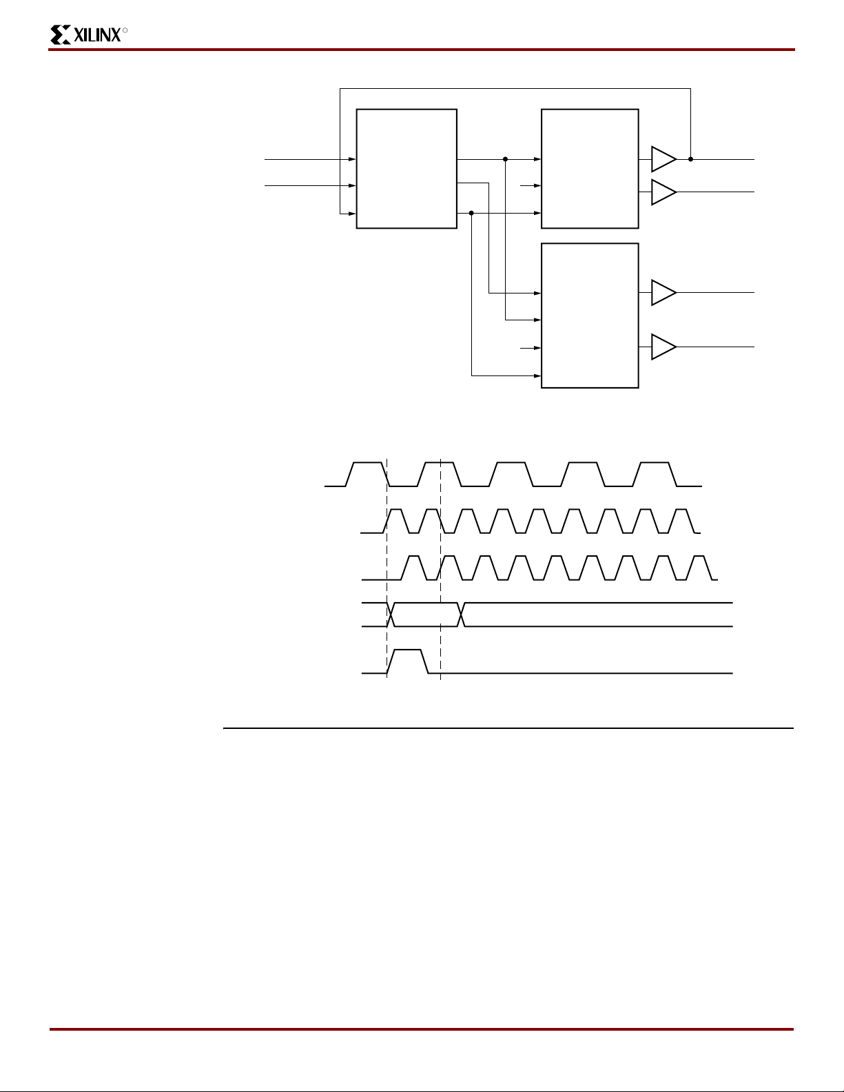
Clocking
Scheme
The clocking scheme for this design includes one digital clock manager (DCM) and two phasematched clock dividers (PMCDs) as shown in Figure 1. The controller is clocked at half the
frequency of the interface using CLKdiv_0. Therefore, the address, bank address, and
command signals (RAS_L, CAS_L, and WE_L) are asserted for two clock cycles (known as
"2T" timing), of the fast memory interface clock. The control signals (CS_L, CKE, and ODT) are
twice the rate (DDR) of the half frequency clock CLKdiv_0, ensuring that the control signals are
asserted for just one clock cycle of the fast memory interface clock. The clock is forwarded to
the external memory device using the Output Dual Data Rate (ODDR) flip-flops in the Virtex-4
I/O. This forwarded clock is 180 degrees out of phase with CLKfast_0. Figure 2 shows the
command and control timing diagram.
© 2005 – 2006 Xilinx, Inc. All rights reserved. XILINX, the Xilinx logo, and other designated brands included herein are trademarks of Xilinx, Inc.
All other trademarks are the property of their respective owners.
Page 2
R
56 Memory Interfaces Solution Guide March 2006
Write Datapath
CLKfast Input
System Reset*
CLKIN
RST
CLKFB
DCM
CLK0
LOCKED
CLK90
*
PMCD#1
CLKA
RST
CLKFB
CLKA1
CLKA1D2
CLKfast_0
CLKdiv_0
PMCD#2
CLKA
CLKA1
CLKB
*
RST
CLKA1D2
CLKFB
CLKfast_90
CLKdiv_90
x702_04_051105
Figure 1: Clocking Scheme for the High-Performance Memory Interface Design
CLKdiv_0
CLKfast_0
Memory Device
Clock
Command WRITE IDLE
Control (CS_L)
X721_02_080205
Figure 2: Command and Control Timing
Write Datapath The write datapath uses the built-in OSERDES available in every Virtex-4 I/O. The OSERDES
transmits the data (DQ) and strobe (DQS) signals. The memory specification requires DQS to
be transmitted center-aligned with DQ. The strobe (DQS) forwarded to the memory is
180 degrees out of phase with CLKfast_0. Therefore, the write data transmitted using
OSERDES must be clocked by CLKfast_90 and CLKdiv_90 as shown in Figure 3. The timing
diagram for write DQS and DQ is shown in Figure 4.
Page 3
Write Datapath
March 2006 Memory Interfaces Solution Guide 57
Write
Data
Words
0-3
R
D1
DQ
D2
D3
D4
OSERDES
CLKDIV CLK
CLKdiv_90
CLKfast_90
IOB ChipSyncTM Circuit
Figure 3: Write Data Transmitted Using OSERDES
CLKfast_0
CLKfast_90
Clock Forwarded
to Memory Device
Command WRITE IDLE
Control (CS_L)
Strobe (DQS)
X721_03_080305
Data (DQ), OSERDES Output
D0 D1 D2 D3
X721_04_120505
Figure 4: Write Strobe (DQS) and Data (DQ) Timing for a Write Latency of Four
Page 4
R
58 Memory Interfaces Solution Guide March 2006
Write Timing Analysis
Ta bl e 1 shows the write timing analysis for an interface at 333 MHz (667 Mb/s).
Ta b l e 1 : Write Timing Analysis at 333 MHz
Write Datapath
Uncertainty Parameters Value
T
CLOCK
T
MEMORY_DLL_DUTY_CYCLE_DIST
T
DATA_PERIOD
T
SETUP
T
HOLD
T
PACKAGE_SKEW
T
JITTER
T
CLOCK_SKEW-MAX
T
CLOCK_OUT_PHASE
Uncertainties
before DQS
Uncertainties
after DQS
Meaning
3000 Clock period.
150 150 150 Duty-cycle distortion from memory DLL is
subtracted from clock phase (equal to half
the clock period) to determine
T
DATA_PERIOD.
1350 Data period is half the clock period with 10%
duty-cycle distortion subtracted from it.
100 100 0 Specified by memory vendor.
175 0 175 Specified by memory vendor.
30 30 30 PCB trace delays for DQS and its
associated DQ bits are adjusted to account
for package skew. The listed value
represents dielectric constant variations.
50 50 50 Same DCM used to generate DQS and DQ.
50 50 50 Global Clock Tree skew.
140 140 140 Phase offset error between different clock
outputs of the same DCM.
T
PCB_LAYOUT_SKEW
50 50 50 Skew between data lines and the
associated strobe on the board.
Total Uncertainties 420 495
Start and End of Valid Window 420 855
Final Window 435 Final window equals 855 – 420.
Notes:
1. Skew between output flip-flops and output buffers in the same bank is considered to be minimal over voltage and temperature.
Page 5

Write Datapath
March 2006 Memory Interfaces Solution Guide 59
Controller to Write Datapath Interface
Ta bl e 2 lists the signals required from the controller to the write datapath.
Ta b l e 2 : Controller to Write Datapath Signals
R
Signal Name
Signal
Width
Signal Description Notes
ctrl_WrEn 1 Output from the controller to the write
datapath.
Write DQS and DQ generation
begins when this signal is asserted.
ctrl_wr_disable 1 Output from the controller to the write
datapath.
Write DQS and DQ generation ends
when this signal is deasserted.
ctrl_Odd_Latency 1 Output from controller to write
datapath.
Asserted when the selected CAS
latency is an odd number, e.g., 5.
Required for generation of write DQS
and DQ after the correct write
latency (CAS latency – 1).
Asserted for two CLKDIV_0 cycles for a burst length
of 4 and three CLKDIV_0 cycles for a burst length of
8.
Asserted one CLKDIV_0 cycle earlier than the
WRITE command for CAS latency values of 4 and
5.
Figure 5 and Figure 6 show the timing relationship
of this signal with respect to the WRITE command.
Asserted for one CLKDIV_0 cycle for a burst length
of 4 and two CLKDIV_0 cycles for a burst length of
8.
Asserted one CLKDIV_0 cycle earlier than the
WRITE command for CAS latency values of 4 and
5.
Figure 5 and Figure 6 show the timing relationship
of this signal with respect to the WRITE command.
Page 6

R
60 Memory Interfaces Solution Guide March 2006
Write Datapath
CLKdiv_0
Clock Forwarded
to Memory Device
CLKdiv_90
CLKfast_90
Command
WRITE IDLE
Control (CS_L)
ctrl_WrEn
ctrl_wr_disable
User Interface Data
FIFO Out
OSERDES Inputs D1, D2, D3, D4
OSERDES Inputs T1, T2, T3, T4
D0,D1,D2,D3
X,X,D0,D1
1,1,0,0
D2,D3,X,X
0,0,1,1
Strobe (DQS)
Data (DQ), OSERDES Output
D0 D1 D2 D3
X721_05_080205
Figure 5: Write DQ Generation with a Write Latency of 4 and a Burst Length of 4
CLKdiv_0
CLKfast_0
Clock Forwarded
to Memory Device
CLKdiv_180
Command
WRITE IDLE
Control (CS_L)
ctrl_WrEn
ctrl_wr_disable
OSERDES Inputs D1, D2, D3, D4
OSERDES Inputs T1, T2, T3, T4
0, 0, 0, 0
1, 1, 1, 0
0, 1, 0, 1
0, 0, 0, 0
0, 0, 0 ,0
0, 1, 1, 1
Strobe (DQS), OSERDES Output
X721_06_080205
Figure 6: Write DQS Generation for a Write Latency of 4 and a Burst Length of 4
Page 7

Read Datapath
March 2006 Memory Interfaces Solution Guide 61
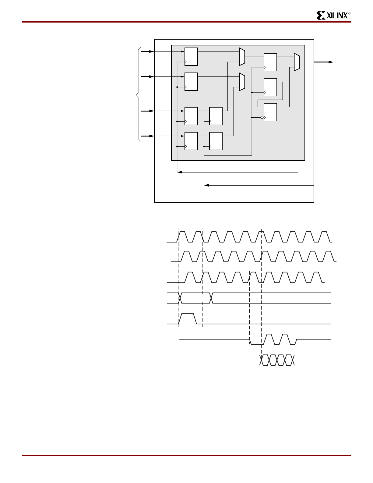
Read Datapath The read datapath comprises the read data capture and recapture stages. Both stages are
implemented in the built-in ISERDES available in every Virtex-4 I/O. The ISERDES has three
clock inputs: CLK, OCLK, and CLKDIV. The read data is captured in the CLK (DQS) domain,
recaptured in the OCLK (FPGA fast clock) domain, and finally transferred to the CLKDIV
(FPGA divided clock) domain to provide parallel data.
N CLK: The read DQS routed using BUFIO provides the CLK input of the ISERDES as
shown in Figure 7.
N OCLK: The OCLK input of ISERDES is connected to the CLK input of OSERDES in
hardware. In this design, the CLKfast_90 clock is provided to the ISERDES OCLK input
and the OSERDES CLK input. The clock phase used for OCLK is dictated by the phase
required for write data.
N CLKDIV: It is imperative for OCLK and CLKDIV clock inputs to be phase-aligned for
correct functionality. Therefore, the CLKDIV input is provided with CLKdiv_90 that is
phase-aligned to CLKfast_90.
User Interface
FIFOs
DQ
Delay
Read Data
to Align With
Strobe and
FPGA Clock
Q1
Q2
Read Data
Word 3
Read Data
Word 2
R
IOB
Q3
Q4
Read Data
Word 1
Read Data
Word 0
ISERDES
CLK OCLK CLKDIV
BUFIO
DQS
Data Delay Value Determined
Using Training Pattern
CLKdiv_90
CLKfast_90
X721_07_063005
Figure 7: Read Data Capture Using ISERDES
Read Timing Analysis
To capture read data without errors in the ISERDES, read data and strobe must be delayed to
meet the setup and hold times of the flip-flops in the FPGA clock domain. Read data (DQ) and
strobe (DQS) are received edge-aligned at the FPGA. The differential DQS pair must be placed
on a clock-capable IO pair in order to access the BUFIO resource. The received read DQS is
then routed through the BUFIO resource to the CLK input of the ISERDES of the associated
data bits. The delay through the BUFIO and clock routing resources shifts the DQS to the right
with respect to data. The total delay through the BUFIO and clock resource is 595 ps in a -11
speed grade device and 555 ps in a -12 speed grade device.
Page 8

R
62 Memory Interfaces Solution Guide March 2006
Read Datapath
Ta bl e 3 shows the read timing analysis at 333 MHz required to determine the delay required on
DQ bits for centering DQS in the data valid window.
Table 3: Read Timing Analysis at 333 MHz
Parameter Value (ps) Meaning
T
CLOCK
T
PHASE
T
SAMP_BUFIO
3000 Clock period.
1500 Clock phase for DDR data.
350 Sample Window from Virtex-4 data sheet for
a -12 device. It includes setup and hold for
an IOB FF, clock jitter, and 150 ps of tap
uncertainty.
T
BUFIO_DCD
T
DQSQ + TQHS
100 BUFIO clock resource duty-cycle distortion.
580 Worst case memory uncertainties that
include VT variations and skew between
DQS and its associated DQs. Because the
design includes per bit deskew, realistically
only a percentage of this number should be
considered.
T
MEM_DCD
150 Duty-cycle distortion.
Tap Uncertainty 0 Tap uncertainty with 75 ps resolution. A
window detection error of 75 ps can be on
both ends of the window. This is already
included in T
SAMP_BUFIO
.
Total Uncertainties 1180
Window 320 Worst-case window.
Notes:
1. T
SAMP_BUFIO
the BUFIO clocking resource and the IDELAY.
2. All the parameters listed above are uncertainties to be considered when using the per bit
calibration technique.
3. Parameters like BUFIO skew, package_skew, pcb_layout_skew, and part of TDQSQ, and
TQHS are calibrated out with the per bit calibration technique. Inter-symbol interference and
crosstalk, contributors to dynamic skew, are not considered in this analysis.
is the sampling error over VT for a DDR input register in the IOB when using
Per Bit Deskew Data Capture Technique
To ensure reliable data capture in the OCLK and CLKDIV domains in the ISERDES, a training
sequence is required after memory initialization. The controller issues a WRITE command to
write a known data pattern to a specified memory location. The controller then issues
back-to-back read commands to read back the written data from this specified location. The DQ
bit 0 ISERDES outputs Q1, Q2, Q3, and Q4 are then compared with the known data pattern. If
they do not match, DQ and DQS are delayed by one tap, and the comparison is performed
again. The tap increments continue until there is a match. If there is no match even at tap 64,
then DQ and DQS are both reset to tap 0. DQS tap is set to one, and both DQS and DQ are
delayed in unit tap increments and the comparison is performed after each tap increment until
a match is found. With the first detected match, the DQS window count is incremented to 1.
DQS continues to be delayed in unit tap increments until a mismatch is detected. The DQS
window count is also incremented along with the tap increments to record the width of the data
valid window in the FPGA clock domain. DQS is then decremented by half the window count to
center DQS edges in the center of the data valid window. With the position of DQS fixed, each
DQ bit is then centered with respect to DQS. The dp_dly_slct_done signal is asserted when the
centering of all DQ bits associated with its DQS is completed.
Page 9

Read Datapath
March 2006 Memory Interfaces Solution Guide 63
CLKdiv_0
CLKfast_0
CLKfast_90
CLKdiv_90
R
Figure 8 shows the timing waveform for read data and strobe delay determination. The
waveforms on the left show a case where the DQS is delayed due to BUFIO and clocking
resource, and the ISERDES outputs do not match the expected data pattern. The waveforms
on the right show a case where the DQS and DQ are delayed until the ISERDES outputs match
the expected data pattern. The lower end of the frequency range useful in this design is limited
by the number of available taps in the IDELAY block, the PCB trace delay, and the CAS latency
of the memory device.
DQS @ FPGA
DQ @ FPGA
DQS @ ISERDES
delayed by BUFIO
and clocking resource
DQ Captured in DQS Domain
Input to Q2 Reg
Input to Q1 Reg
CLKfast_90
Domain
Input to Q4 Reg
Input to Q3 Reg
D0 D1 D2 D3
DQ
D0
D1 D2
D0
D1 D3
D0 D2
Parallel Data @ ISERDES
Outputs Q4, Q3, Q2, Q1
DQS @ FPGA
D3
D2
D1 D3
D0 D2
D1
DQ @ FPGA
DQS Delayed by Calibration
Delay @ ISERDES
DQ Delayed by Calibration Delay
D0
D1
No Match
D3
D2,D3,D0,D1
Incorrect Data
Sequence
D0 D1 D2 D3
Figure 8: Read Data and Strobe Delay
D0
D1 D2
D3
D0
D2
D1 D3
D0 D2
D1 D3
Parallel Data @ ISERDES
Outputs Q4, Q3, Q2, Q1
Correct Data
Sequence
D0 D2
D1
D3
D0,D1,D2,D3
X721_08_112905
Page 10

R
64 Memory Interfaces Solution Guide March 2006
Controller to Read Datapath Interface
Ta bl e 4 lists the control signals between the controller and the read datapath.
Ta bl e 4 : Signals between Controller and Read Datapath
Read Datapath
Signal Name
Signal
Width
Signal Description Notes
ctrl_Dummyread_Start 1 Output from the controller to the
read datapath. When this signal
is asserted, the strobe and data
calibration begin.
dp_dly_slct_done 1 Output from the read datapath
to the controller indicating the
strobe and data calibration are
complete.
ctrl_RdEn_div0 1 Output from the controller to the
read datapath used as the write
enable to the read data capture
FIFOs.
This signal must be asserted when valid read data
is available on the data bus.
This signal is deasserted when the
dp_dly_slct_done signal is asserted.
This signal is asserted when the data and strobe
have been calibrated.
Normal operation begins after this signal is
asserted.
This signal is asserted for one CLKdiv_0 clock
cycle for a burst length of 4 and two clock cycles for
a burst length of 8.
The CAS latency and additive latency values
determine the timing relationship of this signal with
the read state.
Figure 9 shows the timing waveform for this signal
with a CAS latency of 5 and an additive latency of
0 for a burst length of 4.
CLKdiv_0
CLKfast_0
CLKdiv_90
CLKfast_90
Command
CS# @ Memory
ctrl_RdEn_div0
(Input to SRL16 Clocked
by CLKdiv_90)
srl_out (SRL16 Output)
Ctrl_RdEn
(Write_enable to FIFOs Aligned with ISERDES Data Output)
READ
Figure 9: Read-Enable Timing for CAS Latency of 5 and Burst Length of 4
D0
D1 D2 D3
D0 D1 D2 D3
DQ @ Memory Device
DQS @ Memory Device
DQS @ ISERDES CLK Input
(Round Trip & BUFIO & Calibration Delays)
DQ @ ISERDES Input
(Round Trip & Initial Tap Value & Calibration Delays)
D0,D1,D2,D3
Parallel Data
@ ISERDES Output
X721_09_113005
Page 11

Reference Design
March 2006 Memory Interfaces Solution Guide 65
R
The ctrl_RdEn signal is required to validate read data because the DDR2 SDRAM devices do
not provide a read valid or read-enable signal along with read data. The controller generates
this read-enable signal based on the CAS latency and the burst length. This read-enable signal
is input to an SRL16 (LUT-based shift register). The number of register stages required to align
the read-enable signal to the ISERDES read data output is determined during calibration. One
read-enable signal is generated for each data byte. Figure 10 shows the read-enable logic
block diagram.
Reference
Design
ctrl_RdEn_div0
srl_out
SRL16
Number of Register Stages
Selected During Calibration
ctrl_RdEn
FD
CLKdiv_90
x721_10_113005
Figure 10: Read-Enable Logic
Figure 11 shows the hierarchy of the reference design. The mem_interface_top is the top-level
module. This reference design is available on the Xilinx website at:
http://www.xilinx.com/bvdocs/appnotes/xapp721.zip
mem_Interface_top
infrastructure
idelay_ctrl
main
.
infrastr_iobs
v4_dqs_iobv4_dm_iobidelay_rd_en_io v4_dq_iob
Figure 11: Reference Design Hierarchy
top test_bench
ddr2_controllerdata_pathuser_interfaceiobs
rd_wr_addr_fifo wr_data_fifo_16 rd_data_fifo tap_ctrl
backend_rom cmp_rd_data
addr_gen data_gen_16tap_logicdata_writerd_databackend_fifosdatapath_iobscontroller_iobs
RAM_D
data_tap_inc
X721_11_113005
Page 12

R
66 Memory Interfaces Solution Guide March 2006
Reference Design Utilization
Reference
Design
Utilization
Ta bl e 5 lists the resource utilization for a 64-bit interface including the physical layer, the
controller, the user interface, and a synthesizable test bench.
Table 5: Resource Utilization for a 64-Bit Interface
Resources Utilization Notes
Slices 5861 Includes the controller, synthesizable test bench, and the user
interface.
BUFGs 6 Includes one BUFG for the 200 MHz reference clock for the
IDELAY block.
BUFIOs 8 Equals the number of strobes in the interface.
DCMs 1
PMCDs 2
ISERDES 64 Equals the number of data bits in the interface.
OSERDES 88 Equals the sum of the data bits, strobes, and data mask bits.
Conclusion The data capture technique explained in this application note using ISERDES provides a good
margin for high-performance memory interfaces. The high margin can be achieved because all
the logic in the FPGA fabric is clocked at half the frequency of the interface, eliminating critical
paths.
Revision
History
The following table shows the revision history for this document.
Date Version Revision
12/15/05 1.0 Initial Xilinx release.
12/20/05 1.1 Updated Ta bl e 1 .
01/04/06 1.2 Updated link to reference design file.
02/02/06 1.3 Updated Ta bl e 4 .
 Loading...