

Page 1

ML361 Virtex-II Pro
DDR400/PC3200 Memory
Board User Guide
UG060 (v1.2) November 8, 2007
R
Page 2
R
Xilinx is disclosing this user guide, manual, release note, and/or specification (the "Documentation") to you solely for use in the development
of designs to operate with Xilinx hardware devices. You may not reproduce, distribute, republish, download, display, post, or transmit the
Documentation in any form or by any means including, but not limited to, electronic, mechanical, photocopying, recording, or otherwise,
without the prior written consent of Xilinx. Xilinx expressly disclaims any liability arising out of your use of the Documentation. Xilinx reserves
the right, at its sole discretion, to change the Documentation without notice at any time. Xilinx assumes no obligation to correct any errors
contained in the Documentation, or to advise you of any corrections or updates. Xilinx expressly disclaims any liability in connection with
technical support or assistance that may be provided to you in connection with the Information.
THE DOCUMENTATION IS DISCLOSED TO YOU “AS-IS” WITH NO WARRANTY OF ANY KIND. XILINX MAKES NO OTHER
WARRANTIES, WHETHER EXPRESS, IMPLIED, OR STATUTORY, REGARDING THE DOCUMENTATION, INCLUDING ANY
WARRANTIES OF MERCHANTABILITY, FITNESS FOR A PARTICULAR PURPOSE, OR NONINFRINGEMENT OF THIRD-PARTY
RIGHTS. IN NO EVENT WILL XILINX BE LIABLE FOR ANY CONSEQUENTIAL, INDIRECT, EXEMPLARY, SPECIAL, OR INCIDENTAL
DAMAGES, INCLUDING ANY LOSS OF DATA OR LOST PROFITS, ARISING FROM YOUR USE OF THE DOCUMENTATION.
© 2004–2007 Xilinx, Inc. All rights reserved.
XILINX, the Xilinx logo, the Brand Window, and other designated brands included herein are trademarks of Xilinx, Inc. All other trademarks
are the property of their respective owners.
ML361 Virtex-II Pro DDR400/PC3200 Memory Board User Guide
UG060 (v1.2) November 8, 2007
The following table shows the revision history for this document.
Version Revision
01/23/04 1.0 Initial Xilinx release.
03/26/04 1.1 Revised Figure 4-6, Figure 4-7, Figure 4-8, Figure 4-9, Figure 4-26, and Figure 4-27.
11/08/07 1.2
• Ta bl e 5 -1 : Typographical corrections.
• Ta bl e B -1 : Deleted Slice Coordinates column from table.
• Updated copyright notice and legal disclaimer.
ML361 Virtex-II Pro Memory Board www.xilinx.com UG060 (v1.2) November 8, 2007
Page 3

Table of Contents
Schedule of Figures. . . . . . . . . . . . . . . . . . . . . . . . . . . . . . . . . . . . . . . . . . . . . . . . . . . . . . . . . . 5
Schedule of Tables . . . . . . . . . . . . . . . . . . . . . . . . . . . . . . . . . . . . . . . . . . . . . . . . . . . . . . . . . . . 7
Preface: About This Guide
Guide Contents . . . . . . . . . . . . . . . . . . . . . . . . . . . . . . . . . . . . . . . . . . . . . . . . . . . . . . . . . . . . . . 9
Additional Resources . . . . . . . . . . . . . . . . . . . . . . . . . . . . . . . . . . . . . . . . . . . . . . . . . . . . . . . . 9
Conventions . . . . . . . . . . . . . . . . . . . . . . . . . . . . . . . . . . . . . . . . . . . . . . . . . . . . . . . . . . . . . . . . 10
Typographical. . . . . . . . . . . . . . . . . . . . . . . . . . . . . . . . . . . . . . . . . . . . . . . . . . . . . . . . . . . . 10
Online Document . . . . . . . . . . . . . . . . . . . . . . . . . . . . . . . . . . . . . . . . . . . . . . . . . . . . . . . . . 10
Chapter 1: Introduction
Overview . . . . . . . . . . . . . . . . . . . . . . . . . . . . . . . . . . . . . . . . . . . . . . . . . . . . . . . . . . . . . . . . . . . 11
Features. . . . . . . . . . . . . . . . . . . . . . . . . . . . . . . . . . . . . . . . . . . . . . . . . . . . . . . . . . . . . . . . . . . . . 12
Chapter 2: Architecture
ML361 Board Block Diagram . . . . . . . . . . . . . . . . . . . . . . . . . . . . . . . . . . . . . . . . . . . . . . . . 13
Block Descriptions . . . . . . . . . . . . . . . . . . . . . . . . . . . . . . . . . . . . . . . . . . . . . . . . . . . . . . . . . . 14
FPGA . . . . . . . . . . . . . . . . . . . . . . . . . . . . . . . . . . . . . . . . . . . . . . . . . . . . . . . . . . . . . . . . . . . 14
Memories . . . . . . . . . . . . . . . . . . . . . . . . . . . . . . . . . . . . . . . . . . . . . . . . . . . . . . . . . . . . . . . . 14
DDR SDRAM DIMM (Banks 6 and 7). . . . . . . . . . . . . . . . . . . . . . . . . . . . . . . . . . . . . . . 14
DDR SDRAM Components (Banks 2 and 3) . . . . . . . . . . . . . . . . . . . . . . . . . . . . . . . . . . 14
DDR SDRAM Component (Bank 1) . . . . . . . . . . . . . . . . . . . . . . . . . . . . . . . . . . . . . . . . 14
RS232 . . . . . . . . . . . . . . . . . . . . . . . . . . . . . . . . . . . . . . . . . . . . . . . . . . . . . . . . . . . . . . . . . . . 14
Clocks. . . . . . . . . . . . . . . . . . . . . . . . . . . . . . . . . . . . . . . . . . . . . . . . . . . . . . . . . . . . . . . . . . . 14
200 MHz LVDS Clock . . . . . . . . . . . . . . . . . . . . . . . . . . . . . . . . . . . . . . . . . . . . . . . . . . . 14
166 MHz LVDS Test Clock . . . . . . . . . . . . . . . . . . . . . . . . . . . . . . . . . . . . . . . . . . . . . . . 15
SMA Clock . . . . . . . . . . . . . . . . . . . . . . . . . . . . . . . . . . . . . . . . . . . . . . . . . . . . . . . . . . . 15
User I/Os. . . . . . . . . . . . . . . . . . . . . . . . . . . . . . . . . . . . . . . . . . . . . . . . . . . . . . . . . . . . . . . . 15
Mictor Connectors . . . . . . . . . . . . . . . . . . . . . . . . . . . . . . . . . . . . . . . . . . . . . . . . . . . . . 15
GPIO . . . . . . . . . . . . . . . . . . . . . . . . . . . . . . . . . . . . . . . . . . . . . . . . . . . . . . . . . . . . . . . . 15
DIP Switch . . . . . . . . . . . . . . . . . . . . . . . . . . . . . . . . . . . . . . . . . . . . . . . . . . . . . . . . . . . 16
Seven-Segment Displays. . . . . . . . . . . . . . . . . . . . . . . . . . . . . . . . . . . . . . . . . . . . . . . . . 16
LEDs . . . . . . . . . . . . . . . . . . . . . . . . . . . . . . . . . . . . . . . . . . . . . . . . . . . . . . . . . . . . . . . . 17
Push Buttons. . . . . . . . . . . . . . . . . . . . . . . . . . . . . . . . . . . . . . . . . . . . . . . . . . . . . . . . . . 17
Grounded I/Os. . . . . . . . . . . . . . . . . . . . . . . . . . . . . . . . . . . . . . . . . . . . . . . . . . . . . . . . 17
Power . . . . . . . . . . . . . . . . . . . . . . . . . . . . . . . . . . . . . . . . . . . . . . . . . . . . . . . . . . . . . . . . . . . 18
Power Distribution . . . . . . . . . . . . . . . . . . . . . . . . . . . . . . . . . . . . . . . . . . . . . . . . . . . . . 18
Input Voltage . . . . . . . . . . . . . . . . . . . . . . . . . . . . . . . . . . . . . . . . . . . . . . . . . . . . . . . . . 18
3.3 V Generation . . . . . . . . . . . . . . . . . . . . . . . . . . . . . . . . . . . . . . . . . . . . . . . . . . . . . . . 18
2.6 V Generation . . . . . . . . . . . . . . . . . . . . . . . . . . . . . . . . . . . . . . . . . . . . . . . . . . . . . . . 18
1.5 V Generation . . . . . . . . . . . . . . . . . . . . . . . . . . . . . . . . . . . . . . . . . . . . . . . . . . . . . . . 18
1.3 V Generation . . . . . . . . . . . . . . . . . . . . . . . . . . . . . . . . . . . . . . . . . . . . . . . . . . . . . . . 18
Linear Regulators for the MGTs . . . . . . . . . . . . . . . . . . . . . . . . . . . . . . . . . . . . . . . . . . . 18
ML361 Virtex-II Pro Memory Board www.xilinx.com 3
UG060 (v1.2) November 8, 2007
Page 4

FPGA Configuration . . . . . . . . . . . . . . . . . . . . . . . . . . . . . . . . . . . . . . . . . . . . . . . . . . . . . . 18
JTAG . . . . . . . . . . . . . . . . . . . . . . . . . . . . . . . . . . . . . . . . . . . . . . . . . . . . . . . . . . . . . . . . 18
PROMs . . . . . . . . . . . . . . . . . . . . . . . . . . . . . . . . . . . . . . . . . . . . . . . . . . . . . . . . . . . . . . 19
Chapter 3: Electrical Requirements
Power Consumption . . . . . . . . . . . . . . . . . . . . . . . . . . . . . . . . . . . . . . . . . . . . . . . . . . . . . . . . 21
FPGA Internal Power Budget. . . . . . . . . . . . . . . . . . . . . . . . . . . . . . . . . . . . . . . . . . . . . . . . 22
Chapter 4: Signal Integrity Recommendations and Simulations
Termination and Transmission Line Summaries . . . . . . . . . . . . . . . . . . . . . . . . . . . . . 25
Terminations and Transmission Lines for DDR Components . . . . . . . . . . . . . . . . . . . 26
Data and Clock Signals (DQ, DQS, DM, CLK) . . . . . . . . . . . . . . . . . . . . . . . . . . . . . . . . 26
Address and Control Signals (A, BA, RASn, CASn, WEn, CSn, CKE) . . . . . . . . . . . . . . 26
Terminations and Transmission Lines for the DIMM . . . . . . . . . . . . . . . . . . . . . . . . . . 27
Data and Clock Signals (DQ, DQS, DM, CLK) . . . . . . . . . . . . . . . . . . . . . . . . . . . . . . . . 27
Address and Control Signals (A, BA, RASn, CASn, WEn, CSn, CKE) . . . . . . . . . . . . . . 27
Duty Cycle Summary . . . . . . . . . . . . . . . . . . . . . . . . . . . . . . . . . . . . . . . . . . . . . . . . . . . . . . . 27
IBIS Simulations . . . . . . . . . . . . . . . . . . . . . . . . . . . . . . . . . . . . . . . . . . . . . . . . . . . . . . . . . . . . 29
Notes on the Simulation Results . . . . . . . . . . . . . . . . . . . . . . . . . . . . . . . . . . . . . . . . . . . . 30
Data Signal Simulations . . . . . . . . . . . . . . . . . . . . . . . . . . . . . . . . . . . . . . . . . . . . . . . . . . . 31
Data Signals from the FPGA to Memory (SSTL2_C2 at FPGA). . . . . . . . . . . . . . . . . . . . 32
Data Signals from the Last Memory to the FPGA: Measured at FPGA. . . . . . . . . . . . . . 36
Clock Signal Simulations . . . . . . . . . . . . . . . . . . . . . . . . . . . . . . . . . . . . . . . . . . . . . . . . . . 40
Address and Control Signal Simulations . . . . . . . . . . . . . . . . . . . . . . . . . . . . . . . . . . . . . 45
Simulations with 10% Tolerance on the Transmission Line Impedance . . . . . . . . . . . 56
Data Signals . . . . . . . . . . . . . . . . . . . . . . . . . . . . . . . . . . . . . . . . . . . . . . . . . . . . . . . . . . 56
Clock Signals. . . . . . . . . . . . . . . . . . . . . . . . . . . . . . . . . . . . . . . . . . . . . . . . . . . . . . . . . . 60
Address/Control Signals . . . . . . . . . . . . . . . . . . . . . . . . . . . . . . . . . . . . . . . . . . . . . . . . 62
R
Chapter 5: Board Layout Guidelines
Decoupling Guidelines . . . . . . . . . . . . . . . . . . . . . . . . . . . . . . . . . . . . . . . . . . . . . . . . . . . . . 65
Providing Additional Ground Pins . . . . . . . . . . . . . . . . . . . . . . . . . . . . . . . . . . . . . . . . . . 67
Board Stackup Guidelines. . . . . . . . . . . . . . . . . . . . . . . . . . . . . . . . . . . . . . . . . . . . . . . . . . . 67
Appendix A: Related Documentation
Appendix B: FPGA Pinout
4 www.xilinx.com ML361 Virtex-II Pro Memory Board
UG060 (v1.2) November 8, 2007
Page 5

Schedule of Figures
Chapter 1: Introduction
Figure 1-1: Simplified Block Diagram of Memory Board Interfaces . . . . . . . . . . . . . . . . . 11
Chapter 2: Architecture
Figure 2-1: ML361 Board Block Diagram. . . . . . . . . . . . . . . . . . . . . . . . . . . . . . . . . . . . . . . . . 13
Chapter 3: Electrical Requirements
Chapter 4: Signal Integrity Recommendations and Simulations
Figure 4-1: Data Signal Terminations. . . . . . . . . . . . . . . . . . . . . . . . . . . . . . . . . . . . . . . . . . . . 31
Figure 4-2: Data Signal from FPGA to Memory (Typical Case) . . . . . . . . . . . . . . . . . . . . . 32
Figure 4-3: Data Signal from FPGA to Memory (Slow Weak Case). . . . . . . . . . . . . . . . . . 33
Figure 4-4: Data Signal from FPGA to Memory (Fast Strong Case) . . . . . . . . . . . . . . . . . . 34
Figure 4-5: Eye Diagram for Data from the FPGA to Last Memory Component. . . . . . . 35
Figure 4-6: Data Signal from Last Memory at FPGA (Typical Case) . . . . . . . . . . . . . . . . . 36
Figure 4-7: Data Signal from Last Memory at FPGA (Slow Weak Corner Case). . . . . . . 37
Figure 4-8: Data Signal from Memory at FPGA (Fast Strong Corner Case) . . . . . . . . . . . 38
Figure 4-9: Eye Diagram for Data at the FPGA to the Last Memory Component . . . . . . 39
Figure 4-10: Clock Signal Terminations. . . . . . . . . . . . . . . . . . . . . . . . . . . . . . . . . . . . . . . . . . 40
Figure 4-11: Clock Signal from FPGA to Memory (Typical Case) . . . . . . . . . . . . . . . . . . . 41
Figure 4-12: Clock Signal from FPGA to Memory (Slow Weak Case). . . . . . . . . . . . . . . . 42
Figure 4-13: Clock Signal from FPGA to Memory (Fast Strong Case) . . . . . . . . . . . . . . . . 43
Figure 4-14: Eye Diagram for Clock at Memory . . . . . . . . . . . . . . . . . . . . . . . . . . . . . . . . . . . 44
Figure 4-15: Address and Control Signal Terminations . . . . . . . . . . . . . . . . . . . . . . . . . . . . 45
Figure 4-16: Address/Control Signals for All Memories . . . . . . . . . . . . . . . . . . . . . . . . . . . 46
Figure 4-17: Address/Control Signals at First DDR Memory (Typical Case). . . . . . . . . . 47
Figure 4-18: Address/Control Signals at First DDR Memory (Slow Weak Case) . . . . . . 48
Figure 4-19: Address/Control Signals at First DDR Memory (Fast Strong Case) . . . . . . 49
Figure 4-20: Address/Control Signals at Last DDR Memory (Typical Case) . . . . . . . . . . 50
Figure 4-21: Address/Control Signals at Last DDR Memory (Slow Weak Case). . . . . . . 51
Figure 4-22: Address/Control Signals at Last DDR Memory (Fast Strong Corner Case) 52
Figure 4-23: Address/Control Signals at Middle DDR Memory (Typical Case) . . . . . . . 53
Figure 4-24: Address/Control Signals at Middle DDR Memory (Slow Weak Corner
Case) . . . . . . . . . . . . . . . . . . . . . . . . . . . . . . . . . . . . . . . . . . . . . . . . . . . . . . . . . . . . . . . . . . . . . . 54
Figure 4-25: Address/Control Signals at Middle DDR Memory (Fast Strong Corner
Case) . . . . . . . . . . . . . . . . . . . . . . . . . . . . . . . . . . . . . . . . . . . . . . . . . . . . . . . . . . . . . . . . . . . . . . 55
Figure 4-26: Data Signals from Last DDR Memory to FPGA (45Ω Impedance) . . . . . . . 56
Figure 4-27: Data Signals from Last DDR Memory to FPGA (55Ω Impedance) . . . . . . . 57
Figure 4-28: Data Signals from FPGA to Last DDR Memory (45Ω Impedance) . . . . . . . 58
ML361 Virtex-II Pro Memory Board www.xilinx.com 5
UG060 (v1.2) November 8, 2007
Page 6

Figure 4-29: Data Signals from Memory to FPGA (55Ω Impedance) . . . . . . . . . . . . . . . . . 59
Figure 4-30: Clock Signals with 45Ω Impedance . . . . . . . . . . . . . . . . . . . . . . . . . . . . . . . . . . 60
Figure 4-31: Clock Signals with 55Ω Impedance . . . . . . . . . . . . . . . . . . . . . . . . . . . . . . . . . . 61
Figure 4-32: Address/Control Signals with 45Ω Impedance Measured at First DDR
Component . . . . . . . . . . . . . . . . . . . . . . . . . . . . . . . . . . . . . . . . . . . . . . . . . . . . . . . . . . . . . . . . 62
Figure 4-33: Address/Control Signals with 55Ω Impedance Measured at First DDR
Component . . . . . . . . . . . . . . . . . . . . . . . . . . . . . . . . . . . . . . . . . . . . . . . . . . . . . . . . . . . . . . . . 63
Chapter 5: Board Layout Guidelines
Appendix A: Related Documentation
Appendix B: FPGA Pinout
R
6 www.xilinx.com ML361 Virtex-II Pro Memory Board
UG060 (v1.2) November 8, 2007
Page 7

Schedule of Tables
Chapter 1: Introduction
Chapter 2: Architecture
Table 2-1: GPIO Header 1 . . . . . . . . . . . . . . . . . . . . . . . . . . . . . . . . . . . . . . . . . . . . . . . . . . . . . . 15
Table 2-2: GPIO Header 2 . . . . . . . . . . . . . . . . . . . . . . . . . . . . . . . . . . . . . . . . . . . . . . . . . . . . . . 16
Table 2-3: DIP Switch Connections. . . . . . . . . . . . . . . . . . . . . . . . . . . . . . . . . . . . . . . . . . . . . . 16
Table 2-4: Display 1 . . . . . . . . . . . . . . . . . . . . . . . . . . . . . . . . . . . . . . . . . . . . . . . . . . . . . . . . . . . 16
Table 2-5: Display 2 . . . . . . . . . . . . . . . . . . . . . . . . . . . . . . . . . . . . . . . . . . . . . . . . . . . . . . . . . . . 17
Table 2-6: LED Connections to FPGA. . . . . . . . . . . . . . . . . . . . . . . . . . . . . . . . . . . . . . . . . . . . 17
Chapter 3: Electrical Requirements
Table 3-1: ML361 Power Consumption . . . . . . . . . . . . . . . . . . . . . . . . . . . . . . . . . . . . . . . . . . 21
Table 3-2: XC2VP20FF1152 Estimated Power Consumption . . . . . . . . . . . . . . . . . . . . . . . . 22
Table 3-3: XC2VP20FF1152 Temperature Specifications. . . . . . . . . . . . . . . . . . . . . . . . . . . . 22
Table 3-4: Device Quiescent Power. . . . . . . . . . . . . . . . . . . . . . . . . . . . . . . . . . . . . . . . . . . . . . 22
Table 3-5: CLB Logic Power . . . . . . . . . . . . . . . . . . . . . . . . . . . . . . . . . . . . . . . . . . . . . . . . . . . . 23
Table 3-6: Digital Clock Manager Power . . . . . . . . . . . . . . . . . . . . . . . . . . . . . . . . . . . . . . . . . 23
Table 3-7: Input/Output Power . . . . . . . . . . . . . . . . . . . . . . . . . . . . . . . . . . . . . . . . . . . . . . . . . 24
Chapter 4: Signal Integrity Recommendations and Simulations
Table 4-1: DDR SDRAM Terminations . . . . . . . . . . . . . . . . . . . . . . . . . . . . . . . . . . . . . . . . . . 25
Table 4-2: DIMM Terminations. . . . . . . . . . . . . . . . . . . . . . . . . . . . . . . . . . . . . . . . . . . . . . . . . 25
Table 4-3: Duty Cycle Summary . . . . . . . . . . . . . . . . . . . . . . . . . . . . . . . . . . . . . . . . . . . . . . . . 27
Chapter 5: Board Layout Guidelines
Table 5-1: FPGA Decoupling Capacitors . . . . . . . . . . . . . . . . . . . . . . . . . . . . . . . . . . . . . . . . . 65
Table 5-2: DDR SDRAM Decoupling Capacitors . . . . . . . . . . . . . . . . . . . . . . . . . . . . . . . . . 66
Table 5-3: DIMM Decoupling Capacitors . . . . . . . . . . . . . . . . . . . . . . . . . . . . . . . . . . . . . . . . 66
Table 5-4: 16-Layer Board Stackup . . . . . . . . . . . . . . . . . . . . . . . . . . . . . . . . . . . . . . . . . . . . . . 67
Appendix A: Related Documentation
Appendix B: FPGA Pinout
Table B-1: FPGA Pinout. . . . . . . . . . . . . . . . . . . . . . . . . . . . . . . . . . . . . . . . . . . . . . . . . . . . . . . . 71
ML361 Virtex-II Pro Memory Board www.xilinx.com 7
UG060 (v1.2) November 8, 2007
Page 8

R
8 www.xilinx.com ML361 Virtex-II Pro Memory Board
UG060 (v1.2) November 8, 2007
Page 9
R
About This Guide
This document describes the design of the ML361 Virtex-II Pro™ DDR400/PC3200
Memory Board, which connects a Virtex-II Pro FPGA to DDR memories.
Guide Contents
This manual contains the following chapters:
• Chapter 1, “Introduction,” describes the purpose of the ML361 board and provides its
key features.
• Chapter 2, “Architecture,” provides a block diagram of the memory board and
describes the key components.
• Chapter 3, “Electrical Requirements,” lists the electrical specifications for the memory
board.
• Chapter 4, “Signal Integrity Recommendations and Simulations,” provides
information on termination, transmission lines, and duty cycles. It also gives the
results of several IBIS simulations.
• Chapter 5, “Board Layout Guidelines,” provides information on decoupling
capacitors, ground signals, and PCB layout.
• Appendix A, “Related Documentation,” lists data sheet and external website
references specific to the ML361 components.
• Appendix B, “FPGA Pinout,” provides the pinout of the Virtex-II Pro FPGA.
Preface
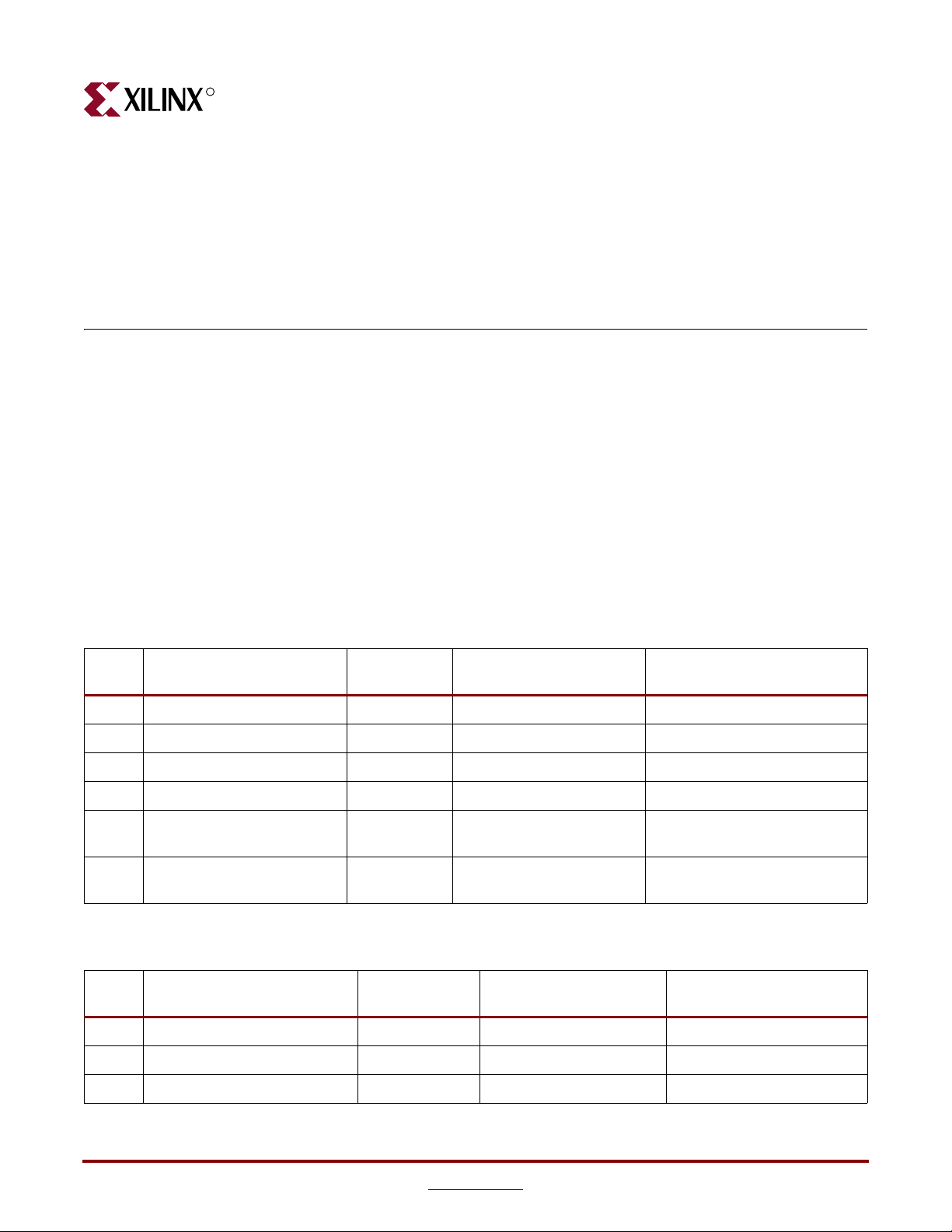
Additional Resources
For additional information, go to http://support.xilinx.com. The following table lists
some of the resources you can access from this website. You can also directly access these
resources using the provided URLs.
Resource Description/URL
Tutorials Tutorials covering Xilinx design flows, from design entry to verification
and debugging
http://support.xilinx.com/support/techsup/tutorials/index.htm
Answer Browser Database of Xilinx solution records
http://support.xilinx.com/xlnx/xil_ans_browser.jsp
Application Notes Descriptions of device-specific design techniques and approaches
http://support.xilinx.com/apps/appsweb.htm
ML361 Virtex-II Pro Memory Board www.xilinx.com 9
UG060 (v1.2) November 8, 2007
Page 10
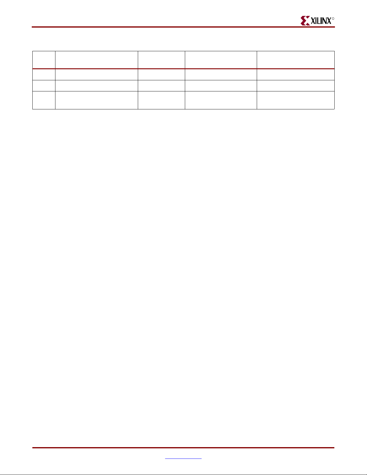
Preface: About This Guide
Data Sheets Device-specific information on Xilinx device characteristics, including
Problem Solvers Interactive tools that allow you to troubleshoot your design issues
Tech Tips Latest news, design tips, and patch information for the Xilinx design
Conventions
This document uses the following conventions. An example illustrates each convention.
Typographical
The following typographical conventions are used in this document:
R
Resource Description/URL
readback, boundary scan, configuration, length count, and debugging
http://support.xilinx.com/xlnx/xweb/xil_publications_index.jsp
http://support.xilinx.com/support/troubleshoot/psolvers.htm
environment
http://www.support.xilinx.com/xlnx/xil_tt_home.jsp
Convention Meaning or Use Example
Italic font
Online Document
The following conventions are used in this document:
Convention Meaning or Use Example
Blue text
Blue, underlined text
References to other manuals
Emphasis in text
Cross-reference link to a location
in the current document
Hyperlink to a website (URL)
See the Development System
Reference Guide for more
information.
If a wire is drawn so that it
overlaps the pin of a symbol, the
two nets are not connected.
See the section “Additional
Resources” for details.
Refer to “Title Formats” in
Chapter 1 for details.
Go to http://www.xilinx.com
for the latest speed files.
10 www.xilinx.com ML361 Virtex-II Pro Memory Board
UG060 (v1.2) November 8, 2007
Page 11
R
Introduction
Overview
The ML361 Virtex-II Pro DDR400/PC3200 Memory Board provides a communications
platform between a Virtex-II Pro FPGA and high-speed double-data-rate (DDR) memories
with operating speeds up to 200 MHz. The ML361 has three major functions:
• Tests and verifies the interoperability of Virtex-II Pro devices with high-speed DDR
memories
• Serves as a development platform for Xilinx and its customers to use for building
memory controllers
• Provides a means by which Xilinx can demonstrate high-speed DDR memory
interoperability
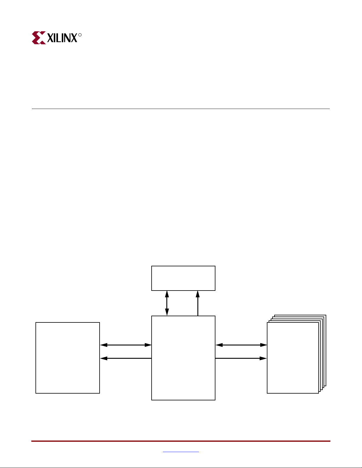
Chapter 1
X-Ref Target - Figure 1-1
DDR
SDRAM DIMM
128MB
(MT4VDDT1664-AG-40BC3)
This document describes the functional blocks within the ML361. It also provides various
recommendations and requirements for usage of the board, including electrical
requirements, logic analyzer requirements, and signal integrity issues. Simulation results
using IBIS also are included.
Figure 1-1 shows a simplified block diagram of the ML361 memory interfaces.
DDR SDRAM
(MT46V32M8TG-5B)
Data (8 bits)
Data (72 bits)
Address/Control
Virtex-II Pro FPGA
XC2VP20FF1152-6
Address/Control
Data (72 bits)
Address/Control
DDR
SDRAMs
256Mb
(4 MT46V16M16TG-5B
and
1 MT46V32M8TG-5B)
ug060_c1_01_012104
Figure 1-1: Simplified Block Diagram of Memory Board Interfaces
ML361 Virtex-II Pro Memory Board www.xilinx.com 11
UG060 (v1.2) November 8, 2007
Page 12

Chapter 1: Introduction
Features
R
The ML361 demonstrates a 64-/72-bit interface to a 128 MByte, 200 MHz DDR SDRAM
DIMM, a 72-bit interface to five 256 Mbit, 200 MHz DDR SDRAM components, and an
additional 8-bit interface to a 256 Mbit, 200 MHz DDR SDRAM component on one of the
top banks.
The key features of the ML361 are summarized below:
• One Virtex-II Pro FPGA (XC2VP20FF1152-6)
• One DDR SDRAM DIMM (MT4VDDT1664-AG-40BC3)
♦ 128 MBytes
♦ 64-/72-bit data interface
• Five DDR SDRAMs (four MT46V16M16TG-5B devices and one MT46V32M8TG-5B
device)
♦ 1.28 Gbits
♦ 72-bit data interface
• One DDR SDRAM (MT46V32M8TG-5B)
♦ 256 Mbits
♦ 8-bit data interface
• Two separate controllers for each 72-bit memory interface
• 200 MHz interface
• The memory interfaces are located on the FPGA left/right interface and top I/O
banks (banks 1, 2, 3, 6, and 7)
12 www.xilinx.com ML361 Virtex-II Pro Memory Board
UG060 (v1.2) November 8, 2007
Page 13
R
Architecture
This chapter provides functional descriptions of the major blocks within the ML361 board
design. For more detailed information on the design, refer to the schematics, which are
located at http://www.xilinx.com/bvdocs/userguides/ug060.zip
ML361 Board Block Diagram
Figure 2-1 shows a block diagram of the ML361 board. Refer to the following section for
additional information on the major blocks.
X-Ref Target - Figure 2-1
5V
Input
Jack
JTAG Port
PROM
7-Segment Displays
DIP Switch
Chapter 2
.
Serial Port
3.3V Regulator
Switch
1.3V Regulator
2.6V Regulator
(5.5A)
2.6V Regulator
(10A)
(5.5A)
(10A)
GPIO Header GPIO Header
CLOCK
(200 MHz)
DDR SDRAM
(x16)
DDR SDRAM
(x16)
DDR SDRAM
(x16)
DDR SDRAM
(x16)
DDR SDRAM
(x8)
MICTOR (38-pin) MICTOR (38-pin)
XC2VP20FF1152C-6
DDR SDRAM
CLOCK
(166 MHz)
(x8)
Push1 Push2 Prgm Reset
Figure 2-1: ML361 Board Block Diagram
DDR
SDRAM
DIMM
(x64)
ug060_c2_01_121703
ML361 Virtex-II Pro Memory Board www.xilinx.com 13
UG060 (v1.2) November 8, 2007
Page 14

Chapter 2: Architecture
Block Descriptions
This section describes the major blocks of the ML361 board.
FPGA
The ML361 uses a Xilinx XC2VP20FF1152C-6 Virtex-II Pro device. This device is packaged
in a 1152-pin BGA package with a -6 speed grade. Refer to Appendix B, “FPGA Pinout,”for
a complete pinout of the Virtex-II Pro device.
Memories
The ML361 board supports two types of memories: DDR SDRAM DIMM and DDR
SDRAM.
DDR SDRAM DIMM (Banks 6 and 7)
The DDR SDRAM DIMM used on the ML361 board is a 184-pin, 200 MHz, unbuffered,
non-ECC Micron MT4VDDT1664-AG-40BC3 device. This DIMM module has a 64-bit wide
data interface. The board also has provisions to interface to a 72-bit wide DIMM.
R
DDR SDRAM Components (Banks 2 and 3)
DDR SDRAM Component (Bank 1)
RS232
Clocks
200 MHz LVDS Clock
The ML361 board contains five 200 MHz DDR SDRAM components that provide a 72-bit
interface. These devices include four 16-bit Micron MT46V16M16TG-5B devices and one
MT46V32M8TG-5B DDR SDRAM devices. They are packaged in 66-pin TSOP packages.
They share a common address and control bus and have separate clocks and DQS/DQ
signals.
The ML361 board contains one 8-bit Micron MT46V32M8TG-5B device on the top bank of
the FPGA.
The ML361 board provides an RS232 serial interface using a Texas Instruments
MAX3221CDBR device. The maximum speed of this device is 250 Kb/s. The RS232
interface is accessible through a female DB9 RA connector.
The ML361 board contains 166 MHz and 200 MHz LVDS clock oscillators and connectors
for external LVDS clock inputs.
The LVDS clock is a Pletronics LV1145BW-200.0M oscillator with a differential output. The
oscillator runs at 200 MHz ± 50 PPM with an operating voltage of 2.5 V ± 5%. It is
terminated at the FPGA with a 100
CLK_200_LVDSP and CLK_200_LVDSN inputs, respectively.
14 www.xilinx.com ML361 Virtex-II Pro Memory Board
Ω resistor. FPGA pins J17 and H17 in Bank 1 serve as the
UG060 (v1.2) November 8, 2007
Page 15
R
166 MHz LVDS Test Clock
SMA Clock
User I/Os
Mictor Connectors
Block Descriptions
The LVDS test clock is a Pletronics SM7745DW-100.0M clock oscillator with a single-ended
output. This oscillator runs at 166 MHz ± 50 PPM with an operating voltage of 2.5 V ± 5%.
FPGA pins E17 and D17 in Bank 1 serve as the CLK_166_LVDSP and CLK_166_LVDSN
inputs, respectively.
Two SMA connectors are provided for the input of an off-board differential clock. The
traces from the SMAs are run as a pair to the FPGA where they are terminated with a
100 ohm resistor. AK18 serves as the CLK_SMAP input, and AL18 serves as the
CLK_SMAN input for the SMA connector pair.
This subsection describes the devices that connect to the User I/Os of the ML361 board.
The FPGA interfaces to two 38-pin Mictor connectors. They can be used to hook up to a
logic analyzer. All signals from the FPGA to the connectors are matched closely. Refer to
the Xilinx data sheets in Appendix A, “Related Documentation,” for more information.
GPIO
The ML361 board contains 16 general-purpose I/Os (GPIOs), which are accessible through
two 2 x 8 0.100" pin headers (see Ta bl e 2 -1 and Tab le 2 - 2). The even-numbered pins on each
header are connected to ground. The GPIO header pins can be accessed through I/Os in
Bank 0.
Table 2-1: GPIO Header 1
GPIO Pin # FPGA I/O Pin
G00 F22
G01 E22
G02 E25
G03 D25
G04 H21
G05 D22
G06 D23
G07 D24
ML361 Virtex-II Pro Memory Board www.xilinx.com 15
UG060 (v1.2) November 8, 2007
Page 16
Chapter 2: Architecture
DIP Switch
II
Table 2-2: GPIO Header 2
GPIO Pin # FPGA I/O Pin
G08 D30
G09 D29
G10 K23
G11 J23
G12 H22
G13 G22
G14 D26
G15 C26
One eight-position DIP switch is connected to the FPGA I/Os as shown in Ta bl e 2 -3 . These
switches can be used to externally pull up or pull down any signal on the FPGA.
R
Table 2-3: DIP Switch Connections
DIP Switch Input FPGA I/O Pin #
DIP1 G26
DIP2 H25
DIP3 G25
DIP4 J25
DIP5 K24
DIP6 J24
DIP7 F26
DIP8 E26
Seven-Segment Displays
Two seven-segment displays connect to the FPGA I/Os (see Tab le 2- 4 and Ta bl e 2 - 5). The
red displays are active Low. The decimal points are not connected.
Table 2-4: Display 1
DIsplay Input FPGA I/O Pin #
Display1A C21
Display1B E21
Display1C F21
Display1D J20
Display1E K20
16 www.xilinx.com ML361 Virtex-II Pro Memory Board
UG060 (v1.2) November 8, 2007
Page 17
R
Block Descriptions
Table 2-4: Display 1
DIsplay Input FPGA I/O Pin #
Display1F C24
Display1G D24
Table 2-5: Display 2
DIsplay Input FPGA I/O Pin #
Display2A D20
Display2B D21
Display2C F20
Display2D G20
Display2E K19
Display2F L19
Display2G C22
LEDs
Four green LEDs connect to the FPGA I/Os as indicated in Ta bl e 2 -6 . The LEDs are active
Low.
Table 2-6: LED Connections to FPGA
LED # FPGA I/O Pin #
LED1 L18
LED2 K18
LED3 G18
LED4 F18
Push Buttons
The ML361 board contains four momentary push buttons. Their functions are as follows:
• Program the FPGA
• Reset the board
• User function 1
• User function 2
Grounded I/Os
Unused I/Os are connected to GND in all FPGA banks. However, all memory banks have
eight unused I/Os connected to GND through 0
Ω resistors. These can be depopulated
when needed for test purposes. Care must be taken to not drive any unused I/Os
connected to GND.
ML361 Virtex-II Pro Memory Board www.xilinx.com 17
UG060 (v1.2) November 8, 2007
Page 18

Chapter 2: Architecture
Power
Power Distribution
Input Voltage
3.3 V Generation
2.6 V Generation
R
The ML361 board uses a 5V input voltage source to generate all the on-board voltages
(1.3V, 1.5V, 2.6V, and 3.3V, and the 2.5V for the MGTs)
The input voltage is specified at 5 V @ 6.5 A. The recommended power supply is a CUI Inc.
DTS050650UTC-PSP-SZ. The jack used is a 4-pin barrel jack, CUI stack PJ-002A-SMT. The
slide switch is a CW Industries G1123-0009. This power input has alternate input solder
pads.
The Texas Instruments PTH05000WAH voltage regulator generates the 3.3 V @ 5.5 A
power. This power input has alternate input solder pads.
The Texas Instruments PTH05010WAS voltage regulator generates the 2.6 V @ 10 A power.
This regulator provides 2.5 Vout with ± 10% trim. This power input has alternate input
solder pads.
1.5 V Generation
The Texas Instruments PTH05000WAH voltage regulator generates the 1.5 V @ 5.5 A
power. This power input has alternate input solder pads.
1.3 V Generation
The Texas Instruments PTH05000WAH voltage regulator generates the 1.3 V @ 1.5 A
power.
Linear Regulators for the MGTs
The Texas Instruments TPS78625 voltage regulator generates 2.5 V @ 1.5 A power for the
Multi Gigabit Transceivers (MGTs).
FPGA Configuration
The Virtex-II Pro FPGA can be programmed through either the JTAG interface or three onboard PROMs.
JTAG
Two headers are used for JTAG: a standard header and a parallel-IV header.
Standard Header
The standard JTAG header is a 1 x 7 0.100" RA header.
Parallel-IV Header
The parallel-IV headers is a 2 x 7 2 mm RA shrouded header.
18 www.xilinx.com ML361 Virtex-II Pro Memory Board
UG060 (v1.2) November 8, 2007
Page 19
R
Block Descriptions
PROMs
The ML361 board contains XCF04S PROMs that can be used to program the
Virtex-II Pro FPGA. The PROM operates with a 3.3 V core voltage and a 2.5 V I/O voltage.
ML361 Virtex-II Pro Memory Board www.xilinx.com 19
UG060 (v1.2) November 8, 2007
Page 20

Chapter 2: Architecture
R
20 www.xilinx.com ML361 Virtex-II Pro Memory Board
UG060 (v1.2) November 8, 2007
Page 21
R
Electrical Requirements
Power Consumption
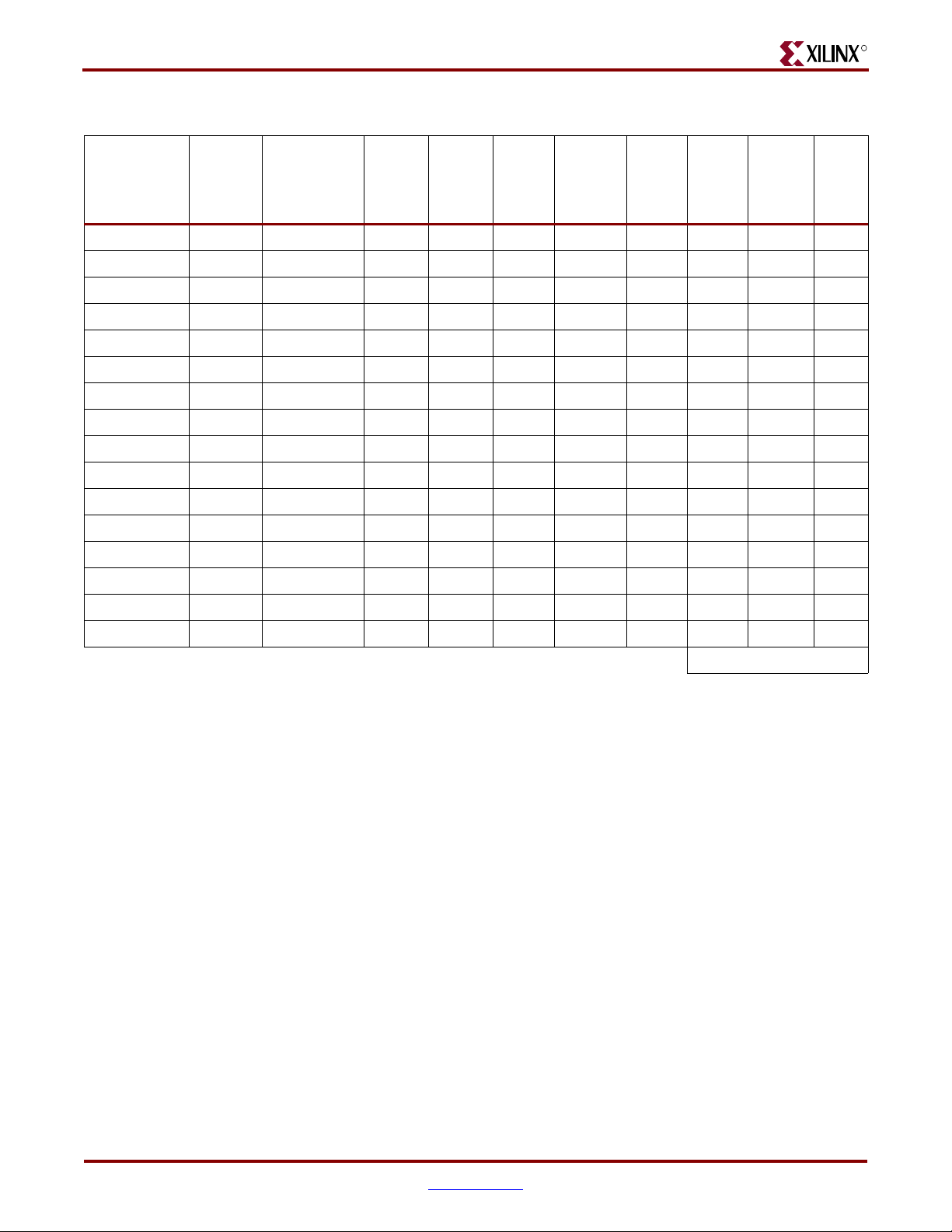
Tab le 3- 1 lists the operating voltages, maximum currents, and power consumption used by
the ML361 board devices. Refer to Appendix A, “Related Documentation,” for more
information on the source material.
Table 3-1: ML361 Power Consumption
Chapter 3
Device Quantity
Total Available Power
Power Supply 1 5 6500 32.5
FPGA Power (Based on Design)
FPGA (XC2VP20-6 FF1152) 1 6.873 Power Estimator Tool
Board Power
Static Power-on Termination
Resistors (50Ω)
DDR SDRAM (72-bit interface) 5 2.6 260 3.38 Micron DDR SDRAM Data Sheet
DDR SDRAM (8-bit interface) 1 2.6 260 0.676
DDR SDRAM DIMM 1 2.6 1040 2.704 Micron DDR SDRAM DIMM Data
200 MHz LVDS Clock Oscillator 1 3.3 40 0.132 Pletronics LV1145B-200 Data Sheet
166 MHz LVDS Clock Oscillator 1 3.3 40 0.132 Pletronics LV1145B-166 Data Sheet
PROMs (XCF04SV020C) 3 2.6 25 0.2 Estimated
375 1.3 16.2 4.92 Virtex-II Pro User Guide (SSTL2
3 3.3 25 0.25 Estimated
Volt ag e
(V)
Current
(mA)
Power
(W)
Source
current specification)
Sheet
8-pin GPIO Header 2 2.6 160 0.416 Average 10 mA * 16 pins
Seven Segment Display 2 2.6 86 0.224 Fourteen 130Ω loads
LEDs 9 2.6 25 0.585 Nine 130Ω loads
DIP Switch 1 2.6 6 0.016 Eight 3.3 kΩ pull-ups
RS232 Serial Port 1 3.3 40 0.132 TI MAX3221 Data Sheet
Worst Case Power Consumption: 20.64
ML361 Virtex-II Pro Memory Board www.xilinx.com 21
UG060 (v1.2) November 8, 2007
Page 22
Chapter 3: Electrical Requirements
FPGA Internal Power Budget
The following tables show the power consumption values inside the FPGA based on the
complete DDR design. These results are derived using the Xilinx Power Estimator tool.
Block Select RAM, Block Multiplier, Processor, and MGT Power tables are not included in
this section as they are not used in this application.
• Tab le 3- 2, “XC2VP20FF1152 Estimated Power Consumption,” page 22
• Tab le 3- 3, “XC2VP20FF1152 Temperature Specifications,” page 22
• Tab le 3- 4, “Device Quiescent Power,” page 22
• Tab le 3- 5, “CLB Logic Power,” page 23
• Tab le 3- 6, “Digital Clock Manager Power,” page 23
• Tab le 3- 7, “Input/Output Power,” page 24
Table 3-2: XC2VP20FF1152 Estimated Power Consumption
Parameter Value Units
Total Estimated Design Power 6873 mW
R
Estimated Design VCC
Estimated Design VCC
1.5 V Power 3811 mW
INT
2.5 V Power 417 mW
AUX
Estimated Design VCCO 3.3 V Power 0 mW
Estimated Design VCCO 2.5 V Power 2645 mW
Estimated Design VCCO 1.8V Power 0 mW
Estimated Design VCCO 1.5 V Power 0 mW
Estimated Design VCCO 1.2 V Power 0 mW
Estimated Design VCC
Estimated Design VCC
Estimated Design VT
Estimated Design VT
RX 2.5 V Power 0 mW
AUX
TX 2.5 V Power 0 mW
AUX
2.5 V Power 0 mW
RX
2.5 V Power 0 mW
TX
Table 3-3: XC2VP20FF1152 Temperature Specifications
Parameter Value Units
Ambient Temperature 25 •C
Air Flow 0 LFM
Junction Temperature 107 •C
Table 3-4: Device Quiescent Power
VCC
Subtotal (mW) VCC
INT
Subtotal (mW)
AUX
450 417
22 www.xilinx.com ML361 Virtex-II Pro Memory Board
UG060 (v1.2) November 8, 2007
Page 23
R
Table 3-5: CLB Logic Power
FPGA Internal Power Budget
Tot al
Name
User Module 1 200 2597 2603 0 1088 40% High 2439
User Module 2 0 0 0 0 0 0% Low 0
User Module 3 0 0 0 0 0 0% Low 0
User Module 4 0 0 0 0 0 0% Low 0
User Module 5 0 0 0 0 0 0% Low 0
User Module 6 0 0 0 0 0 0% Low 0
User Module 7 0 0 0 0 0 0% Low 0
User Module 8 0 0 0 0 0 0% Low 0
User Module 9 0 0 0 0 0 0% Low 0
User Module 10 0 0 0 0 0 0% Low 0
User Module 11 0 0 0 0 0 0% Low 0
User Module 12 0 0 0 0 0 0% Low 0
Frequency
(MHz)
Number
of CLB
Slices
Tot al
Number of
Flip/Flop or
Latches
Tota l N u m be r
of Shift
Register LUTs
Tot al Numbe r
of Select
RAM LUTs
Average
Toggle
Rate
%
Amount of
Routing
Used
Total 2439
VCC
Subtotal
(mW)
INT
Table 3-6: Digital Clock Manager Power
Name
Clock Input
Frequency (MHz)
DCM Frequency Mode
VCC
INT
User DCM 1 200 Low 6
User DCM 2 200 Low 6
User DCM 3 0 Low 0
User DCM 4 0 Low 0
User DCM 5 0 Low 0
User DCM 6 0 Low 0
User DCM 7 0 Low 0
User DCM 8 0 Low 0
User DCM 9 0 Low 0
User DCM 10 0 Low 0
User DCM 11 0 Low 0
User DCM 12 0 Low 0
To t al 1 2
Subtotal
(mW)
ML361 Virtex-II Pro Memory Board www.xilinx.com 23
UG060 (v1.2) November 8, 2007
Page 24
Chapter 3: Electrical Requirements
Table 3-7: Input/Output Power
Average
Output
Enable
Rate
%
Average
Output
Load
(pF)
IOB
Registers
VCC
INT
Subtotal
(mW)
VCCO
Subtotal
Name
Frequency
(MHz)
I/O Standard
Typ e
Tot al
Number
of Inputs
Tot al
Number
Outputs
of
Average
IOB
Tog gle
Rate
%
Jpheader 200 LVCMOS25_12 0 16 25% 100% 0 SDR 2 30
ddr_dq 200 SSTL2_II 138 138 80% 50% 5 DDR 462 877
ddr_dqs 2000 SSTL2_II 18 18 80% 50% 5 DDR 335 363
ddr_address 200 SSTL2_II 0 15 25% 100% 3 SDR 1 106
ddr_control 200 SSTL2_II 0 5 25% 100% 3 SDR 0 35
dimm_address 200 SSTL2_I_DCI 0 15 25% 100% 12 SDR 13 157
dimm_control 200 SSTL2_I_DCI 0 4 50% 100% 12 SDR 12 96
ddr_clks 200 SSTL2_II 0 2 100% 100% 3 DDR 0 42
Display 200 LVCMOS25_12 0 14 6% 100% 0 SDR 1 6
dimm_control_1 200 SSTL2_II 0 3 50% 100% 12 SDR 0 28
ddr_dm 200 SSTL2_II 0 17 10% 100% 5 SDR 2 100
R
(mW)
dimm_clks 200 SSTL2_II 0 6 100% 100% 12 SDR 1 82
top_dq 200 SSTL2_II_DCI 8 8 80% 50% 5 DDR 39 366
top_dqs 200 SSTL2_II_DCI 1 1 80% 50% 5 DDR 15 103
top_address 200 SSTL2_I_DCI 0 15 25% 100% 5 SDR 13 153
top_control 200 SSTL2_I_DCI 0 5 25% 100% 5 SDR 12 95
Total 910 2645
24 www.xilinx.com ML361 Virtex-II Pro Memory Board
UG060 (v1.2) November 8, 2007
Page 25
R
Chapter 4
Signal Integrity Recommendations and
Simulations
This chapter provides the following information:
• Summary of the termination schemes for various signals (“Termination and
Transmission Line Summaries,” page 25)
• Summary of the observed duty cycles for all signals in the IBIS simulations (“Duty
Cycle Summary,” page 27)
• IBIS simulations and duty cycle measurements (“IBIS Simulations,” page 29)
Termination and Transmission Line Summaries
Tab le 4- 1 summarizes the terminations for the five DDR SDRAM components at the FPGA
and at memory.
Table 4-1: DDR SDRAM Terminations
No. Signal
1 Data (DQ) SSTL2_C2 50Ω pull up to 1.3 V 50Ω pull-up to 1.3 V
2 Data Strobe (DQS) SSTL2_C2 50Ω pull up to 1.3 V 50Ω pull-up to 1.3 V
3 Data Mask (DM) SSTL2_C2 50Ω pull up to 1.3 V 50Ω pull-up to 1.3 V
4 Clock (CK, CKn) SSTL2_C2 50Ω pull up to 1.3 V 50Ω pull-up to 1.3 V
5 Address (A, BA) SSTL2_C2 No termination 50Ω pull-up to 1.3 V after the
6 Control (RASn, CASn, WEn,
CSn, CKE)
Tab le 4- 2 summarizes the terminations for the DIMM at the FPGA and at memory.
Table 4-2: DIMM Terminations
No. Signal
Drivers at the
FPGA
SSTL2_C2 No termination 50Ω pull-up to 1.3 V after the
Drivers at the
FPGA
Termination at FPGA Termination at Memory
last component
last component
Termination at FPGA Termination at Memory
1 Data (DQ) SSTL2_C2 50Ω pull-up to 1.3 V 50Ω pull-up to 1.3 V
2 Data Strobe (DQS) SSTL2_C2 50Ω pull-up to 1.3 V 50Ω pull-up to 1.3 V
3 Data Mask (DM) SSTL2_C2 50Ω pull-up to 1.3 V 50Ω pull-up to 1.3 V
ML361 Virtex-II Pro Memory Board www.xilinx.com 25
UG060 (v1.2) November 8, 2007
Page 26
Chapter 4: Signal Integrity Recommendations and Simulations
Table 4-2: DIMM Terminations
R
No. Signal
4 3 pairs of Clocks (CK, CKn) SSTL2_C2 50Ω pull-up to 1.3 V 50Ω pull-up to 1.3 V
5 Address (A, BA) SSTL2_C2_DCI No termination No termination
6 Control (RASn, CASn, WEn,
CSn, CKE and others)
Drivers at the
FPGA
SSTL2_C2_DCI No termination No termination
Termination at FPGA Termination at Memory
Terminations and Transmission Lines for DDR Components
Data and Clock Signals (DQ, DQS, DM, CLK)
For these DDR signals, the terminations at the FPGA and memory consist of a 50Ω parallel
termination pulled up to 1.3 V.
Use 50
Ω transmission lines with less than ± 1% tolerance on the transmission line
impedance. The recommendations for the transmission line lengths are as follows:
• All these data and clock signals are point-to-point from the FPGA to each DDR
component. All signals going to one individual DDR SDRAM component need to be
matched with respect to each other with a ± 2% tolerance.
• All signals going to the first component are matched to a trace length of 2.8 inches
with a ± 2% tolerance. The 2.5 inch requirement includes the FPGA internal package
skew (available on the pinout table) and the skew between the ball of the FPGA to the
resistor pack as well as the length of the actual trace.
• The trace length variation on these signals across the five DDR components is kept as
small as possible to enable data capture while also ensuring they fall within the
address window. The trace lengths on all five DDR components are: 2.8 inches, 2.8
inches, 3.5 inches, 3.8 inches, and 3.8 inches. All signals corresponding to the same
DDR component are matched as close as ± 1% of the above mentioned trace lengths.
Microstrip is used to model the transmission lines in the IBIS simulations.
Address and Control Signals (A, BA, RASn, CASn, WEn, CSn, CKE)
For the address and control signals, no termination is required at the FPGA. At memory, a
50
Ω resistor pulled up to 1.3 V at the end of the daisy chain is required (after the last DDR
component).
Use 50
Ω transmission lines with ± 5% tolerance from the FPGA to all the memory
components. The recommendations for the transmission line lengths are as follows:
• All the signals are routed in a daisy chain fashion.
• There is a maximum of 2.5 inch trace with ± 2% tolerance from the FPGA to the first
DDR component. The 2.5 inch requirement includes the FPGA internal package skew
(that is available on the pinout table) and the skew between the ball of the FPGA to
the resistor pack as well as the length of the actual trace.
• 0.6 inches of distance with ± 2% tolerance is used in the trace length calculations
below between the individual components. Ideally, straight line routing is desired.
During placement, the components are placed as close as 0.5 inches or lesser by
straight line routing, if possible. The main requirement is that all signals going to each
DDR component must be matched by ± 2% tolerance.
26 www.xilinx.com ML361 Virtex-II Pro Memory Board
UG060 (v1.2) November 8, 2007
Page 27
R
• There is a total of 4.9 inches of trace from the FPGA to the last component assuming
the DDR memory components are 0.6 inch apart.
Microstrip is used to model the transmission lines for the first DDR component. All other
DDR components use Buried Microstrip to model the transmission lines.
Terminations and Transmission Lines for the DIMM
Data and Clock Signals (DQ, DQS, DM, CLK)
For these DIMM signals, the terminations at the FPGA and memory consist of a 50Ω
parallel termination pulled up to 1.3 V.
50
Ω transmission lines are used with less than ± 1% tolerance on the transmission line
impedance. The transmission line lengths are as follows:
• There is a 65 mm trace length from FPGA to memory with ± 0.5 mm tolerance.
• A maximum of 1 inch tolerance is allowed to include the FPGA internal package skew
and the skew between the ball of the FPGA to the resistor pack. Package deskew is
necessary if the 1 inch tolerance is not met.
Duty Cycle Summary
Address and Control Signals (A, BA, RASn, CASn, WEn, CSn, CKE)
For the address and control signals, no termination is required at the FPGA or DIMM.
Use 50
Ω transmission lines with less than ± 5% tolerance on the transmission line
impedance. The recommendations for the transmission line lengths are as follows:
• There must be a 65 mm trace length from FPGA to memory with ± 5 mm tolerance.
• Use a maximum of 1 inch tolerance to include the FPGA internal package skew and
the skew between the ball of the FPGA to the resistor pack. Package deskew is
necessary if the 1 inch tolerance is not met.
Duty Cycle Summary
Tab le 4- 3 summarizes the duty cycle measurements taken from prelayout simulations on
50
Ω transmission lines. Refer to “IBIS Simulations,” page 29 for more simulation results.
Table 4-3: Duty Cycle Summary
No. Signal DDR Component Case
1 Address/control Last component
(farthest from FPGA)
Typical 49.22/50.92 NA
Slow weak 49.22/50.63 NA
Duty Cycle
Measured at
Memory(%)
Duty Cycle
Measured at
FPGA (%)
Fast strong 49.22/51.2 NA
2 Address/control First component
(closest to FPGA)
ML361 Virtex-II Pro Memory Board www.xilinx.com 27
UG060 (v1.2) November 8, 2007
Typical 48.94/51.2 NA
Slow weak 49.22/51.48 NA
Fast strong 48.66/51.2 NA
Page 28

Chapter 4: Signal Integrity Recommendations and Simulations
Table 4-3: Duty Cycle Summary
R
No. Signal DDR Component Case
Duty Cycle
Measured at
Memory(%)
Duty Cycle
Measured at
FPGA (%)
3 Address/control Middle component Typical 49.23/51.49 NA
Slow weak 49.22/50.64 NA
Fast strong 48.94/51.2 NA
4 Clock Last component Typical 48.1/52.04 NA
Slow weak 48.66/51.48 NA
Fast strong 48.1/51.48 NA
5 Data Last component Typical 47.24/52.62 48.64/51.78
Slow weak 47.52/52.06 49.52/50.64
Fast strong 46.4/52.9 48.38/51.76
28 www.xilinx.com ML361 Virtex-II Pro Memory Board
UG060 (v1.2) November 8, 2007
Page 29

R
IBIS Simulations
This section summarizes various simulations run on the Memory Board using IBIS. It
defines the test conditions and provides color-coded screen captures of the results. The
resulting signal duty cycles are given also.
The simulations have been divided into the following categories:
1. Data Signal Simulations
2. Clock Signal Simulations
3. Address and Control Signal Simulations
4. Typical Case Simulations with 10% Tolerance for:
IBIS Simulations
a. Data Signals from the FPGA to the Last Memory Component
- Typical Case
- Slow Weak Case
- Fast Strong Case
- Eye Diagram
b. Data Signals from the Last Memory Component to the FPGA
- Typical Case
- Slow Weak Case
- Fast Strong Case
- Eye Diagram
a. Clock Signals from the FPGA to the Last Memory Component
- Typical Case
- Slow Weak Case
- Fast Strong Case
- Eye Diagram
a. Address and Control Signals from the FPGA to the First/Last/Middle Memory
Component
- All Memory Components (Typical Case)
- First DDR Component (Typical, Slow Weak, Fast Strong Cases)
- Last DDR Component (Typical, Fast Strong, Slow Weak Cases)
- Middle DDR Component (Typical, Slow Weak, Fast Strong Cases)
a. Data Signals
- Data Signals from the Last DDR Memory to the FPGA with 45
Ω Transmission
Lines (Typical)
- Data Signals from the Last DDR Memory to the FPGA with 55
Ω Transmission
Lines (Typical)
- Data Signals from the FPGA to the Last DDR Memory with 45
Ω Transmission
Lines (Typical)
- Data Signals from Memory to the FPGA with 55
Ω transmission lines (Typical)
b. Clock Signals
- Clock Signals with 45
- Clock Signals with 55
Ω Transmission Lines (Typical)
Ω Transmission Lines (Typical)
ML361 Virtex-II Pro Memory Board www.xilinx.com 29
UG060 (v1.2) November 8, 2007
Page 30

Chapter 4: Signal Integrity Recommendations and Simulations
c. Address and Control Signals
- Address and Control Signals with 45
DDR Component (Typical)
- Address and Control Signals with 55
DDR Component (Typical)
Notes on the Simulation Results
The provided screen captures show the results of each simulation. The signals in these
screen captures are color-coded as follows:
• Red signal – at FPGA
• Yellow signal – at memory
R
Ω Transmission Lines Measured at First
Ω Transmission Lines Measured at First
The two horizontal yellow lines are V
± 100 mV where V
ref
=1.3 V.
ref
30 www.xilinx.com ML361 Virtex-II Pro Memory Board
UG060 (v1.2) November 8, 2007
Page 31

R
Data Signal Simulations
All data signal simulations below have the following test conditions for typical, slow
weak, and fast strong cases:
IBIS Simulations
• Topology for data signals: 50
• At memory (yellow signal): 50
• At FPGA (red signal): 50
Ω Transmission lines
Ω parallel termination pulled up to 1.3 V
Ω parallel termination pulled up to 1.3 V (SSTL2C2 drivers at
FPGA).
Figure 4-1 shows the data signal terminations.
X-Ref Target - Figure 4-1
ug060_c5_01_091003
Figure 4-1: Data Signal Terminations
ML361 Virtex-II Pro Memory Board www.xilinx.com 31
UG060 (v1.2) November 8, 2007
Page 32

Chapter 4: Signal Integrity Recommendations and Simulations
Data Signals from the FPGA to Memory (SSTL2_C2 at FPGA)
The simulations in this subsection test the data signals from the FPGA to memory.
Simulations were performed for the following cases: typical, slow weak, fast strong. An
eye diagram is provided also.
Typical Case Simulation for Data Signals from the FPGA to the Last DDR
Component
For the typical case simulation, the resulting duty cycle is 47.24/52.62. Figure 4-2 shows
the simulation screen capture for the typical case.
X-Ref Target - Figure 4-2
R
ug060_c5_02_091003
Figure 4-2: Data Signal from FPGA to Memory (Typical Case)
32 www.xilinx.com ML361 Virtex-II Pro Memory Board
UG060 (v1.2) November 8, 2007
Page 33

R
IBIS Simulations
Slow Weak Corner Case for Data from the FPGA to the Last DDR Component
For the slow weak case simulation, the resulting duty cycle is 47.52/52.06. Figure 4-3
shows the simulation screen capture for this case.
X-Ref Target - Figure 4-3
ug060_c5_03_091003
Figure 4-3: Data Signal from FPGA to Memory (Slow Weak Case)
ML361 Virtex-II Pro Memory Board www.xilinx.com 33
UG060 (v1.2) November 8, 2007
Page 34

Chapter 4: Signal Integrity Recommendations and Simulations
Fast Strong Case for Data Signals from the FPGA to the Last DDR Component
For the fast strong case simulation, the resulting duty cycle is 46.4/52.9. Figure 4-4 shows
the simulation screen capture for this case.
X-Ref Target - Figure 4-4
R
ug060_c5_04_091003
Figure 4-4: Data Signal from FPGA to Memory (Fast Strong Case)
34 www.xilinx.com ML361 Virtex-II Pro Memory Board
UG060 (v1.2) November 8, 2007
Page 35

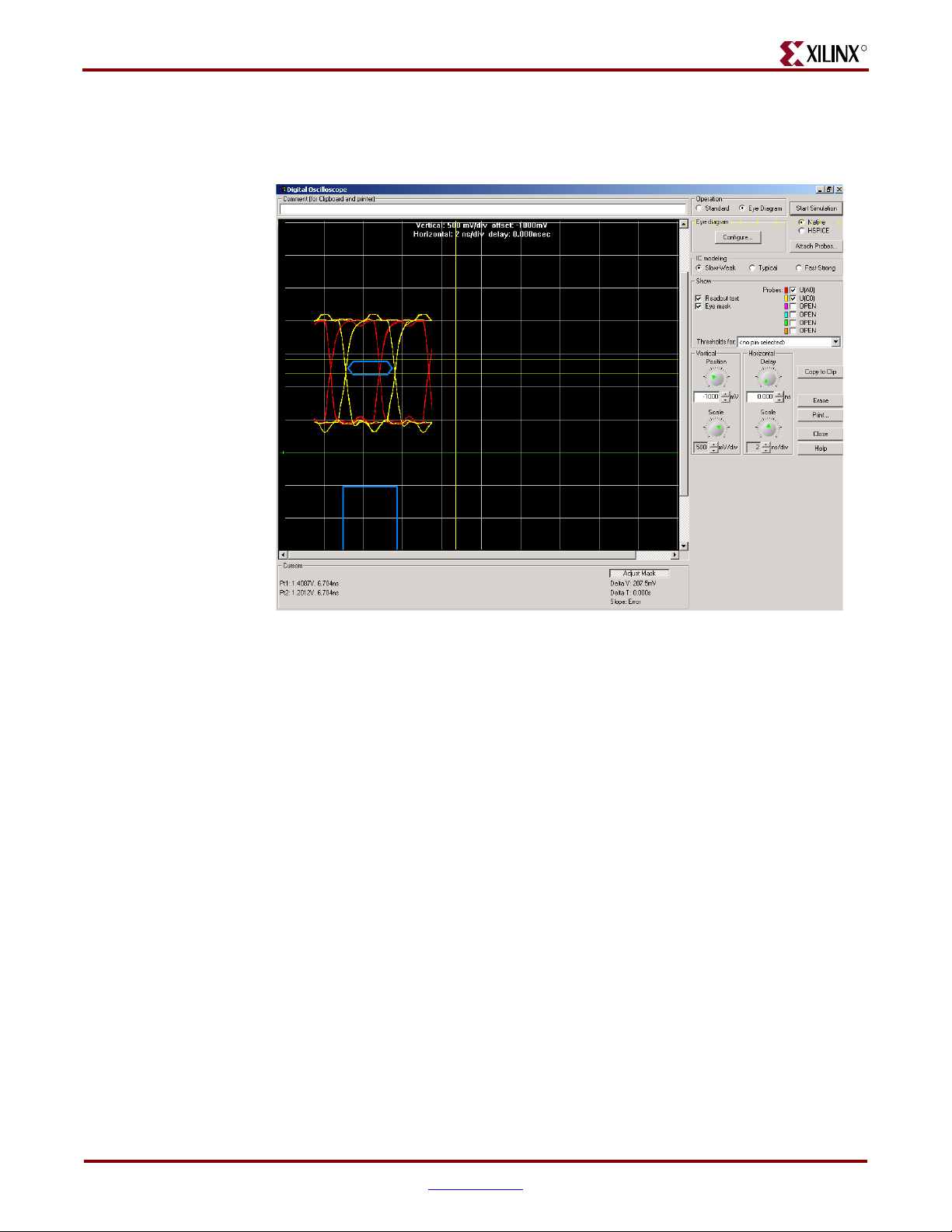
R
IBIS Simulations
Eye Diagram
Figure 4-5 shows the eye diagram for the data signals from the FPGA to the last memory
component.
X-Ref Target - Figure 4-5
ug060_c5_05_091003
Figure 4-5: Eye Diagram for Data from the FPGA to Last Memory Component
ML361 Virtex-II Pro Memory Board www.xilinx.com 35
UG060 (v1.2) November 8, 2007
Page 36

Chapter 4: Signal Integrity Recommendations and Simulations
Data Signals from the Last Memory to the FPGA: Measured at FPGA
The simulations in this subsection test the data signals from the last memory to the FPGA.
Simulations were performed for the following cases: typical, slow weak, and fast strong.
An eye diagram is provided also.
Typical Case for Data from the Last DDR Memory Device to the FPGA
For the typical case simulation, the resulting duty cycle is 48.64/51.78. Figure 4-6 shows
the simulation screen capture for this case.
X-Ref Target - Figure 4-6
R
ug060_c5_06_031204
Figure 4-6: Data Signal from Last Memory at FPGA (Typical Case)
36 www.xilinx.com ML361 Virtex-II Pro Memory Board
UG060 (v1.2) November 8, 2007
Page 37

R
IBIS Simulations
Slow Weak Corner Case for Data Signals from the Last DDR Memory to the FPGA
For the slow weak case simulation, the resulting duty cycle is 49.52/50.64. Figure 4-7
shows the simulation screen capture for this case.
X-Ref Target - Figure 4-7
ug060_c5_07_031204
Figure 4-7: Data Signal from Last Memory at FPGA (Slow Weak Corner Case)
ML361 Virtex-II Pro Memory Board www.xilinx.com 37
UG060 (v1.2) November 8, 2007
Page 38

Chapter 4: Signal Integrity Recommendations and Simulations
Fast Strong Corner Case for Data from Memory to the FPGA
For the fast strong case simulation, the resulting duty cycle is 48.38/51.76. Figure 4-8
shows the simulation screen capture for this case.
X-Ref Target - Figure 4-8
R
ug060_c5_08_031204
Figure 4-8: Data Signal from Memory at FPGA (Fast Strong Corner Case)
38 www.xilinx.com ML361 Virtex-II Pro Memory Board
UG060 (v1.2) November 8, 2007
Page 39

R
IBIS Simulations
Eye Diagram for Data Signal Measured at the FPGA
Figure 4-9 shows the eye diagram for the data signals from the FPGA to the last memory
component.
X-Ref Target - Figure 4-9
ug060_c5_09_031504
Figure 4-9: Eye Diagram for Data at the FPGA to the Last Memory Component
ML361 Virtex-II Pro Memory Board www.xilinx.com 39
UG060 (v1.2) November 8, 2007
Page 40

Chapter 4: Signal Integrity Recommendations and Simulations
Clock Signal Simulations
The simulations in this subsection test the unidirectional clock signals from the FPGA to
memory. Simulations were performed for the following cases: typical, slow weak, and fast
strong. An eye diagram is provided also.
All clock signal simulations below have the following test conditions for typical, slow
weak, and fast strong cases:
R
• Topology for clock signals: 50
• At memory (yellow signal): 50
• At FPGA (red signal): 50
Ω transmission lines
Ω parallel termination pulled up to 1.3 V
Ω parallel termination pulled up to 1.3 V (SSTL2C2 drivers at
FPGA).
Figure 4-10 shows the clock signal terminations.
X-Ref Target - Figure 4-10
ug060_c5_10_091003
Figure 4-10: Clock Signal Terminations
40 www.xilinx.com ML361 Virtex-II Pro Memory Board
UG060 (v1.2) November 8, 2007
Page 41

R
IBIS Simulations
Typical Case for Clock Signals
For the typical case simulation, the resulting duty cycle is 48.1/52.04. Figure 4-11 shows the
simulation screen capture for this case.
X-Ref Target - Figure 4-11
ug060_c5_12_091003
Figure 4-11: Clock Signal from FPGA to Memory (Typical Case)
ML361 Virtex-II Pro Memory Board www.xilinx.com 41
UG060 (v1.2) November 8, 2007
Page 42

Chapter 4: Signal Integrity Recommendations and Simulations
Slow Weak Case for Clock Signals
For the slow weak case simulation, the resulting duty cycle is 48.66/51.48. Figure 4-12
shows the simulation screen capture for this case.
X-Ref Target - Figure 4-12
R
ug060_c5_13_091003
Figure 4-12: Clock Signal from FPGA to Memory (Slow Weak Case)
42 www.xilinx.com ML361 Virtex-II Pro Memory Board
UG060 (v1.2) November 8, 2007
Page 43

R
IBIS Simulations
Fast Strong Case for Clock Signals
For the fast strong case simulation, the resulting duty cycle is 48.1/51.48. Figure 4-13
shows the simulation screen capture for this case.
X-Ref Target - Figure 4-13
ug060_c5_11_091003
Figure 4-13: Clock Signal from FPGA to Memory (Fast Strong Case)
ML361 Virtex-II Pro Memory Board www.xilinx.com 43
UG060 (v1.2) November 8, 2007
Page 44
Chapter 4: Signal Integrity Recommendations and Simulations
Eye Diagram of Clock Signals at Memory
Figure 4-14 shows the eye diagram for the clock signals at memory.
X-Ref Target - Figure 4-14
R
Figure 4-14: Eye Diagram for Clock at Memory
ug060_c5_14_091003
44 www.xilinx.com ML361 Virtex-II Pro Memory Board
UG060 (v1.2) November 8, 2007
Page 45

R
Address and Control Signal Simulations
The simulations in this subsection test the unidirectional address and control signals from
the FPGA to five DDR memory components. Simulations were performed on the first,
middle, and last DDR memory component for the following cases: typical, slow weak, and
fast strong.
All clock signal simulations below have the following test conditions for typical, slow
weak, and fast strong cases:
• Topology: The FPGA and the five DDR components are placed in a straight line in a
daisy chain configuration.
♦ The distance between the FPGA and the first DDR component – 2.1 inches
♦ The distance between adjacent DDR components – 0.7 inches
♦ The distance between the FPGA and the last DDR component – 4.8 inches
• At memory (yellow signal): 50
component.
• At FPGA (red signal): 50
Figure 4-15 shows the address and control signal terminations.
X-Ref Target - Figure 4-15
Ω resistor pulled up to 1.3 V after the last DDR SDRAM
Ω transmission line is used (SSTL2C2 drivers at the FPGA).
IBIS Simulations
ug060_c5_15_091003
Figure 4-15: Address and Control Signal Terminations
ML361 Virtex-II Pro Memory Board www.xilinx.com 45
UG060 (v1.2) November 8, 2007
Page 46

Chapter 4: Signal Integrity Recommendations and Simulations
Typical Case Simulation at All Memory Components
Figure 4-16 shows the simulation screen capture for the typical case for all memory
components.
X-Ref Target - Figure 4-16
R
Figure 4-16: Address/Control Signals for All Memories
ug060_c5_16_091003
46 www.xilinx.com ML361 Virtex-II Pro Memory Board
UG060 (v1.2) November 8, 2007
Page 47

R
IBIS Simulations
Typical Case Simulation at First DDR Component
For the typical case simulation at the first DDR component, the resulting duty cycle is
48.94/51.2. Figure 4-17 shows the simulation screen capture for this case.
X-Ref Target - Figure 4-17
ug060_c5_17_091003
Figure 4-17: Address/Control Signals at First DDR Memory (Typical Case)
ML361 Virtex-II Pro Memory Board www.xilinx.com 47
UG060 (v1.2) November 8, 2007
Page 48

Chapter 4: Signal Integrity Recommendations and Simulations
Slow Weak Corner Case Simulation at First DDR Component
For the slow weak corner case simulation at the first DDR component, the resulting duty
cycle is 49.22/51.48. Figure 4-18 shows the simulation screen capture for this case.
X-Ref Target - Figure 4-18
R
ug060_c5_18_091003
Figure 4-18: Address/Control Signals at First DDR Memory (Slow Weak Case)
48 www.xilinx.com ML361 Virtex-II Pro Memory Board
UG060 (v1.2) November 8, 2007
Page 49

R
IBIS Simulations
Fast Strong Corner Case Simulation at First DDR Component
For the fast strong corner case simulation at the first DDR component, the resulting duty
cycle is 48.66/51.2. Figure 4-19 shows the simulation screen capture for this case.
X-Ref Target - Figure 4-19
ug060_c5_19_091003
Figure 4-19: Address/Control Signals at First DDR Memory (Fast Strong Case)
ML361 Virtex-II Pro Memory Board www.xilinx.com 49
UG060 (v1.2) November 8, 2007
Page 50

Chapter 4: Signal Integrity Recommendations and Simulations
Typical Case Simulation at Last DDR Component
For the typical case simulation at the last DDR component, the resulting duty cycle is
49.22/50.92. Figure 4-20 shows the simulation screen capture for this case.
X-Ref Target - Figure 4-20
R
ug060_c5_20_091003
Figure 4-20: Address/Control Signals at Last DDR Memory (Typical Case)
50 www.xilinx.com ML361 Virtex-II Pro Memory Board
UG060 (v1.2) November 8, 2007
Page 51

R
IBIS Simulations
Slow Weak Case Simulation at Last DDR Component
For the slow weak case simulation at the last DDR component, the resulting duty cycle is
49.22/50.63. Figure 4-21 shows the simulation screen capture for this case.
X-Ref Target - Figure 4-21
ug060_c5_22_091003
Figure 4-21: Address/Control Signals at Last DDR Memory (Slow Weak Case)
ML361 Virtex-II Pro Memory Board www.xilinx.com 51
UG060 (v1.2) November 8, 2007
Page 52

Chapter 4: Signal Integrity Recommendations and Simulations
Fast Strong Corner Case Simulation at Last DDR Component
For the fast strong corner case simulation at the last DDR component, the resulting duty
cycle is 49.22/51.2. Figure 4-22 shows the simulation screen capture for this case.
X-Ref Target - Figure 4-22
R
ug060_c5_21_091003
Figure 4-22: Address/Control Signals at Last DDR Memory (Fast Strong Corner
Case)
52 www.xilinx.com ML361 Virtex-II Pro Memory Board
UG060 (v1.2) November 8, 2007
Page 53

R
IBIS Simulations
Typical Case Simulation at Middle DDR Component
For the typical case simulation at the middle DDR component, the resulting duty cycle is
49.23/51.49. Figure 4-23 shows the simulation screen capture for this case.
X-Ref Target - Figure 4-23
ug060_c5_23_091003
Figure 4-23: Address/Control Signals at Middle DDR Memory (Typical Case)
ML361 Virtex-II Pro Memory Board www.xilinx.com 53
UG060 (v1.2) November 8, 2007
Page 54

Chapter 4: Signal Integrity Recommendations and Simulations
Slow Weak Corner Case Simulation at Middle DDR Component
For the slow weak corner case simulation at the middle DDR component, the resulting
duty cycle is 49.22/50.64. Figure 4-24 shows the simulation screen capture for this case.
X-Ref Target - Figure 4-24
R
ug060_c5_24_091003
Figure 4-24: Address/Control Signals at Middle DDR Memory (Slow Weak Corner
Case)
54 www.xilinx.com ML361 Virtex-II Pro Memory Board
UG060 (v1.2) November 8, 2007
Page 55

R
IBIS Simulations
Fast Strong Corner Case Simulation at Middle DDR Component
For the fast strong corner case simulation at the middle DDR component, the resulting
duty cycle is 48.94/51.2. Figure 4-25 shows the simulation screen capture for this case.
X-Ref Target - Figure 4-25
ug060_c5_25_091003
Figure 4-25: Address/Control Signals at Middle DDR Memory (Fast Strong Corner
Case)
ML361 Virtex-II Pro Memory Board www.xilinx.com 55
UG060 (v1.2) November 8, 2007
Page 56

Chapter 4: Signal Integrity Recommendations and Simulations
Simulations with 10% Tolerance on the Transmission Line Impedance
These simulations illustrate the typical cases for data, clock, and address and control
signals.
Data Signals
This subsection provides the data simulation results for the following typical cases:
R
• From the last DDR memory to the FPGA (45
• From the last DDR memory to the FPGA (55
• From the FPGA to the last DDR memory (45
• From the memory to the FPGA (55
Ω transmission line impedance)
Ω transmission line impedance)
Ω transmission line impedance)
Ω transmission line impedance)
Data Signals from the Last DDR Memory to the FPGA with 45Ω Transmission Line
Impedance
For the typical case simulation from the last DDR component to the FPGA, the resulting
duty cycle is 48.66/51.48. Figure 4-26 shows the simulation screen capture for this case.
X-Ref Target - Figure 4-26
ug060_c5_26_031204
Figure 4-26: Data Signals from Last DDR Memory to FPGA (45Ω Impedance)
56 www.xilinx.com ML361 Virtex-II Pro Memory Board
UG060 (v1.2) November 8, 2007
Page 57

R
IBIS Simulations
Data Signals from the Last DDR Memory to the FPGA with 55Ω Transmission Line
Impedance
For the typical case simulation from the last DDR component to the FPGA, the resulting
duty cycle is 46.4/52.62. Figure 4-27 shows the simulation screen capture for this case.
X-Ref Target - Figure 4-27
ug060_c5_27_031204
Figure 4-27: Data Signals from Last DDR Memory to FPGA (55Ω Impedance)
ML361 Virtex-II Pro Memory Board www.xilinx.com 57
UG060 (v1.2) November 8, 2007
Page 58

Chapter 4: Signal Integrity Recommendations and Simulations
Data Signals from FPGA to the Last DDR Memory Component with 45Ω
Transmission Line Impedance
For the typical case simulation from the FPGA to the last DDR component, the resulting
duty cycle is 46.96/53.18. Figure 4-28 shows the simulation screen capture for this case.
X-Ref Target - Figure 4-28
R
ug060_c5_28_091003
Figure 4-28: Data Signals from FPGA to Last DDR Memory (45Ω Impedance)
58 www.xilinx.com ML361 Virtex-II Pro Memory Board
UG060 (v1.2) November 8, 2007
Page 59

R
IBIS Simulations
Data Signals from Memory to the FPGA with 55Ω Transmission Line Impedance
For the typical case simulation from memory to the FPGA, the resulting duty cycle is
48.66/51.48. Figure 4-29 shows the simulation screen capture for this case.
X-Ref Target - Figure 4-29
ug060_c5_29_091003
Figure 4-29: Data Signals from Memory to FPGA (55Ω Impedance)
ML361 Virtex-II Pro Memory Board www.xilinx.com 59
UG060 (v1.2) November 8, 2007
Page 60

Chapter 4: Signal Integrity Recommendations and Simulations
Clock Signals
This subsection provides the clock simulation results for the following typical cases:
R
• With 45
• With 55
Ω transmission line impedance
Ω transmission line impedance
Clock Signals with 45Ω Transmission Line Impedance
For the typical case simulation with a 45Ω transmission line impedance, the resulting duty
cycle is 48.66/ 52.04. Figure 4-30 shows the simulation screen capture for this case.
X-Ref Target - Figure 4-30
ug060_c5_30_091003
Figure 4-30: Clock Signals with 45Ω Impedance
60 www.xilinx.com ML361 Virtex-II Pro Memory Board
UG060 (v1.2) November 8, 2007
Page 61

R
IBIS Simulations
Clock Signals with 55Ω Transmission Line Impedance
For the typical case simulation with a 55Ω transmission line impedance, the resulting duty
cycle is 48.1/51.48. Figure 4-31 shows the simulation screen capture for this case.
X-Ref Target - Figure 4-31
Figure 4-31: Clock Signals with 55Ω Impedance
ug060_c5_31_091003
ML361 Virtex-II Pro Memory Board www.xilinx.com 61
UG060 (v1.2) November 8, 2007
Page 62

Chapter 4: Signal Integrity Recommendations and Simulations
Address/Control Signals
This subsection provides the address and control simulation results for the following
typical cases:
R
• With 45
• With 55
Ω transmission line impedance measured at the first DDR component
Ω transmission line impedance measured at the first DDR component
Address and Control Signals with 45Ω Transmission Lines Measured at the First
DDR Component
For the typical case simulation with a 45Ω transmission line impedance measured at the
first DDR component, the resulting duty cycle is 48.94/51.2. Figure 4-32 shows the
simulation screen capture for this case.
X-Ref Target - Figure 4-32
ug060_c5_32_091003
Figure 4-32: Address/Control Signals with 45Ω Impedance Measured at First DDR
Component
62 www.xilinx.com ML361 Virtex-II Pro Memory Board
UG060 (v1.2) November 8, 2007
Page 63

R
IBIS Simulations
Address and Control Signals with 55Ω Transmission Lines Measured at the First
DDR Component
For the typical case simulation with a 55Ω transmission line impedance measured at the
first DDR component, the resulting duty cycle is 48.66/51.48. Figure 4-33 shows the
simulation screen capture for this case.
X-Ref Target - Figure 4-33
ug060_c5_33_091003
Figure 4-33: Address/Control Signals with 55Ω Impedance Measured at First DDR
Component
ML361 Virtex-II Pro Memory Board www.xilinx.com 63
UG060 (v1.2) November 8, 2007
Page 64

Chapter 4: Signal Integrity Recommendations and Simulations
R
64 www.xilinx.com ML361 Virtex-II Pro Memory Board
UG060 (v1.2) November 8, 2007
Page 65

R
Board Layout Guidelines
This chapter provides information on decoupling capacitors, ground signals, and PCB
layout.
Decoupling Guidelines
This section lists the decoupling capacitors used with the major components of the ML361
board. Refer to the board schematics for exact placement.
Tab le 5- 1 lists the decoupling capacitors for the Virtex-II Pro FPGA. Refer to the Xilinx
XAPP623
implemented for each bank, VCCI, VAUX, and VREF.
application note for the methodology. A balanced decoupling network is
Chapter 5
Table 5-1: FPGA Decoupling Capacitors
Pin(s) Capacitor Value Distribution
VCCI
1 capacitor per
pin, in a
balanced
decoupling
network.
VA U X
1 capacitor per
pin, in a
balanced
decoupling
network.
Bank 2
39 SSTL2_II
20 SSTL2_I
0.039 µF ceramic capacitor, 0402 10V X7R –20/+20% 10
0.22 µF ceramic capacitor, 0603 10V X7R –20/+20% 5
1 µF ceramic capacitor, 0603 6V X7R –20/+20% 6
10 µF ceramic capacitor, 1206 16V Z5U –20/+20% 3
330 µF solid tantalum capacitor, 6.3V 2
0.039 µF ceramic capacitor, 0402 10V X7R –20/+20% 4
0.22 µF ceramic capacitor, 0603 10V X7R –20/+20% 3
1 µF ceramic capacitor, 0603 6V X7R –20/+20% 3
10 µF ceramic capacitor, 1206 16V Z5U –20/+20% 1
330 µF solid tantalum capacitor, 6.3V 1
Budget = (61/120) = .51 x 12 = 7 caps
0.039 µF ceramic capacitor, 0402 10V X7R –20/+20% 2
0.22 µF ceramic capacitor, 0603 10V X7R –20/+20% 1
1 µF ceramic capacitor, 0603 6V X7R –20/+20% 1
330 µF solid tantalum capacitor, 6.3V 1
ML361 Virtex-II Pro Memory Board www.xilinx.com 65
UG060 (v1.2) November 8, 2007
Page 66

Chapter 5: Board Layout Guidelines
Table 5-1: FPGA Decoupling Capacitors (Cont’d)
Pin(s) Capacitor Value Distribution
R
Bank 2
VREF
7 VREFs used, one capacitor for each VREF
0.039 µF ceramic capacitor, 0402 10V X7R –20/+20% 2
0.22 µF ceramic capacitor, 0603 10V X7R –20/+20% 1
1 µF ceramic capacitor, 0603 6V X7R –20/+20% 1
330 µF solid tantalum capacitor, 6.3V 1, shared with bank 3
Bank 3 Same as Bank 2 for both I/Os and VREFs
Bank 6 Same as Bank 2 for both I/Os and VREFs
Bank 7 Same as Bank 2 for both I/Os and VREFs
Bank 1
1 Reset,
8 GPIO,
4 LED,
8 DIP,
14 DISPLAY
0.033 µF ceramic capacitor, 0402 6V X7R –20/+20% 1
0.22 µF ceramic capacitor, 0603 6V X7R –20/+20% 1
1 µF ceramic capacitor, 0603 6V X7R –20/+20% 1
330 µF solid tantalum capacitor, 6.3V 1
Bank 0 Similar to Bank 1
Bank 4 Similar to Bank 1
Bank 5 Similar to Bank 1
Tab le 5- 2 lists the decoupling capacitors for the DDR SDRAMs.
Table 5-2: DDR SDRAM Decoupling Capacitors
Pin(s) Capacitor Value Quantity Distribution
VDD,
VDDQ,
VREF, VSS,
VSSQ
0.01 µF ceramic capacitor, 0402 6V X7R –20/+20% 8 1 capacitor per pin, in a
0.1 µF ceramic capacitor, 0603 6V X7R –20/+20% 8
balanced decoupling network.
17 total for each component
330 µF solid tantalum capacitor, 6.3V 1
Tab le 5- 3 lists the decoupling capacitors for the DDR DIMM.
Table 5-3: DIMM Decoupling Capacitors
Pin(s) Capacitor Value Distribution
VDD 0.01 µF ceramic capacitor, 0402 6V X7R –20/+20% 1 per VDD pin
0.1 µF ceramic capacitor, 0603 6V X7R –20/+20% 1 per VDD pin
330 µF solid tantalum capacitor, 6.3V 1
VDDQ 0.01 µF ceramic capacitor, 0402 6V X7R –20/+20% 1 per VDDQ pin
0.1 µF ceramic capacitor, 0603 6V X7R –20/+20% 1 per VDDQ pin
330 µF solid tantalum capacitor, 6.3V 2
66 www.xilinx.com ML361 Virtex-II Pro Memory Board
UG060 (v1.2) November 8, 2007
Page 67

R
Providing Additional Ground Pins
Table 5-3: DIMM Decoupling Capacitors (Cont’d)
Pin(s) Capacitor Value Distribution
VREF 0.01 µF ceramic capacitor, 0402 6V X7R –20/+20% 1 VREF to GND
1 VREF to 2.6V
1 GND to 2.6V
0.1 µF ceramic capacitor, 0603 6V X7R –20/+20% 1 VREF to GND
1 VREF to 2.6V
1 GND to 2.6V
VSS 0.01 µF ceramic capacitor, 0402 6V X7R –20/+20% 8
0.1 µF ceramic capacitor, 0603 6V X7R –20/+20% 4
330 µF solid tantalum capacitor, 6.3V 1
Providing Additional Ground Pins
Additional Ground pins can be added by tying unused and no connect pins to GND.
Board Stackup Guidelines
Tab le 5- 4 shows a suggested stackup of a 16-layer board (8 signals, 8 planes).
Table 5-4: 16-Layer Board Stackup
# Type Layer Trace / Spacing Comments
1 Signal TOP 8 mil, 8 mil
2Plane GND GND
3 Plane +2.5V +2.5V separate plane
4 Signal-X IN1 5 mil, 5 mil Route clocks on IN1 and IN2 layers. Can be used for
carefully routing SSTL signals, if routing area needed
5 Signal-Y IN2 5 mil, 5 mil
6Plane +2.6V
7Plane GND
8 Signal-X IN3 5 mil, 5 mil Route all 200 MHz SSTL signals on IN3 and IN4
9 Signal-Y IN4 5 mil, 5 mil
10 Plane GND
11 Plane +1.3V & +1.5V Carve out two power planes on this layer
12 Signal-X IN5 5 mil, 5 mil Route other non-critical signals here
13 Signal-Y IN6 5 mil, 5 mil
14 Plane +3.3V
15 Plane GND
16 Signal BOT 8 mil, 8 mil In the area not used for routing on this layer, add GND fill
to give +3.3V planar capacitance.
ML361 Virtex-II Pro Memory Board www.xilinx.com 67
UG060 (v1.2) November 8, 2007
Page 68

Chapter 5: Board Layout Guidelines
R
68 www.xilinx.com ML361 Virtex-II Pro Memory Board
UG060 (v1.2) November 8, 2007
Page 69

R
Related Documentation
This appendix provides references to documents and web pages for components on the
ML361 board.
• Xilinx, Inc.
♦ Virtex-II Pro X™ Platform FPGAs
http://www.xilinx.com/bvdocs/publications/ds083.pdf
♦ Platform Flash In-System Programmable Configuration PROMs
http://www.xilinx.com/bvdocs/publications/ds123.pdf
• Texa s Inst r umen t s
♦ PTH05000BAH Regulated Step-down DC/DC 5V to 3.3V @ 5.5A
PTH05000FAH Regulated Step-down DC/DC 5V to 1.5V @ 5.5A
http://focus.ti.com/lit/ds/symlink/pth05000w.pdf
Appendix A
♦ PTH05010WAS Regulated Step-down DC/DC 5V to 2.5V @ 10A
http://focus.ti.com/lit/ds/symlink/pth05010w.pdf
♦ MAX3221CDBR RS232 Interface
http://focus.ti.com/lit/ds/symlink/max3221.pdf
• Micron
♦ Micron DDR SDRAM Components
http://download.micron.com/pdf/datasheets/dram/ddr/256Mx4x8x16DDR.pdf
♦ Micron DDR SDRAM DIMM
http://download.micron.com/pdf/datasheets/modules/ddr/DDA4C16_32x64AG.pdf
• Pletronics, Inc.
♦ LV1145BV-166.0M-REX 3.3V High Frequency LVDS Oscillator 166 MHz
LV1145BV-200.0M-REX 3.3V High Frequency LVDS Oscillator 200 MHz
http://www.pletronics.com/LV1100B.HTM
• Agilent Technologies
♦ Logic Analyzer: Agilent Technologies 16753/54/55/56 Logic Analyzer
http://cp.literature.agilent.com/litweb/pdf/5988-9043EN.pdf
♦ Logic Analyzer Probes: Agilent Technologies Connector-based Probes
http://cp.literature.agilent.com/litweb/pdf/16760-97012.pdf
ML361 Virtex-II Pro Memory Board www.xilinx.com 69
UG060 (v1.2) November 8, 2007
Page 70

R
70 www.xilinx.com ML361 Virtex-II Pro Memory Board
UG060 (v1.2) November 8, 2007
Page 71

R
FPGA Pinout
Tab le B -1 summarizes the pinout of the XC2VP20FF1152-6 FPGA in the ML361 board. The
slice coordinates mentioned in Tab le B -1 refer to the RPM grid coordinates corresponding
to the respective I/O pin location. I/O pin names marked as GND refer to unused I/Os
that are directly connected to GND. I/O pin names marked as PULLDOWN refer to
unused I/Os that are connected to GND through a zero ohm resistor. The 0
be removed to use the corresponding I/O for any test purposes.
Table B-1: FPGA Pinout
Appendix B
Ω resistor can
Pin
Numbers
U23 7 VCCO_7
E29 0 IO_L01N_0/VRP_0 RXD 11097.26
E28 0 IO_L01P_0/VRN_0 TXD 10150.32
H26 0 IO_L02N_0 resetN 6327.18
G26 0 IO_L02P_0 DIP1 7905.95
H25 0 IO_L03N_0 DIP2 5691.71
G25 0 IO_L03P_0/VREF_0 DIP3 6996.94
J25 0 IO DIP4 5273.75
K24 0 IO_L06N_0 DIP5 3344.34
J24 0 IO_L06P_0 DIP6 4601.94
F26 0 IO_L07N_0 DIP7 9207.2
E26 0 IO_L07P_0 DIP8 10718.03
D30 0 IO_L08N_0 GPIO08 15834.96
D29 0 IO_L08P_0 GPIO09 14848.81
Virtex-II Pro
Bank Number
Package
Functional Name
I/O Pin Names
Internal Script
Information
Package
Flight Times
(in microns)
K23 0 IO_L09N_0 GPIO10 3066.04
J23 0 IO_L09P_0/VREF_0 GPIO11 4323.64
H22 0 IO_L37N_0 GPIO12 4727.82
G22 0 IO_L37P_0 GPIO13 5923
D26 0 IO_L38N_0 GPIO14 15218.77
C26 0 IO_L38P_0 GPIO15 15469.57
ML361 Virtex-II Pro Memory Board www.xilinx.com 71
UG060 (v1.2) November 8, 2007
Page 72

Table B-1: FPGA Pinout (Cont’d)
R
Pin
Numbers
Virtex-II Pro
Bank Number
Package
Functional Name
I/O Pin Names
Internal Script
Information
Package
Flight Times
(in microns)
K21 0 IO_L39N_0 GND 5505.04
J21 0 IO_L39P_0 GND 4965.14
F22 0 IO_L43N_0 GPIO00 7541.44
E22 0 IO_L43P_0 GPIO01 8910.89
E25 0 IO_L44N_0 GPIO02 12735.3
D25 0 IO_L44P_0 GPIO03 13832.18
H21 0 IO_L45N_0 GPIO04 6364.26
G21 0 IO_L45P_0/VREF_0 GPIO05 7704.24
D22 0 IO_L46N_0 GPIO06 9988.1
D23 0 IO_L46P_0 GPIO07 11050.72
D24 0 IO_L47N_0 DISPLAY1G 12302.96
C24 0 IO_L47P_0 DISPLAY1F 13516.13
K20 0 IO_L48N_0 DISPLAY1E 3126.3
J20 0 IO_L48P_0 DISPLAY1D 4150.17
F21 0 IO_L49N_0 DISPLAY1C 7682.05
E21 0 IO_L49P_0 DISPLAY1B 8634.04
C21 0 IO DISPLAY1A 13499.9
C22 0 IO DISPLAY2G 15061.08
L19 0 IO_L54N_0 DISPLAY2F 2263.39
K19 0 IO_L54P_0 DISPLAY2E 3226.4
G20 0 IO_L55N_0 DISPLAY2D 6227.05
F20 0 IO_L55P_0 DISPLAY2C 7549.54
D21 0 IO_L56N_0 DISPLAY2B 10983.43
D20 0 IO_L56P_0 DISPLAY2A 10275.3
J19 0 IO_L57N_0 GND 3969.14
H19 0 IO_L57P_0/VREF_0 GND 5173.85
G19 0 IO_L67N_0 GND 6064.32
F19 0 IO_L67P_0 GND 8063.93
E19 0 IO_L68N_0 GND 9549.27
D19 0 IO_L68P_0 GND 10957.97
L18 0 IO_L69N_0 LED1 2444
K18 0 IO_L69P_0/VREF_0 LED2 3320.11
G18 0 IO_L73N_0 LED3 5890.16
72 www.xilinx.com ML361 Virtex-II Pro Memory Board
UG060 (v1.2) November 8, 2007
Page 73

R
Table B-1: FPGA Pinout (Cont’d)
Pin
Numbers
Virtex-II Pro
Bank Number
Package
Functional Name
I/O Pin Names
Internal Script
Information
Package
Flight Times
(in microns)
F18 0 IO_L73P_0 LED4 7223.69
E18 0 IO_L74N_0/GCLK7P GND 8692.96
D18 0 IO_L74P_0/GCLK6S GND 9819.09
J18 0 IO_L75N_0/GCLK5P GND 3858.95
H18 0 IO_L75P_0/GCLK4S GND 5131.43
H17 1 IO_L75N_1/GCLK3P CLK_200_LVDSN 5131.43
J17 1 IO_L75P_1/GCLK2S CLK_200_LVDSP 3858.95
D17 1 IO_L74N_1/GCLK1P CLK_166_LDVSN 10242.07
E17 1 IO_L74P_1/GCLK0S CLK_166_LVDSP 8752.34
F17 1 IO_L73N_1 top_clkb 7223.69
G17 1 IO_L73P_1 top_clk 5890.16
K17 1 IO_L69N_1/VREF_1 Vref = 1.3V 3320.11
L17 1 IO_L69P_1 top_dqs 2444
D16 1 IO_L68N_1 top_dq(0) 10931.46
E16 1 IO_L68P_1 top_dq(1) 9549.27
F16 1 IO_L67N_1 top_dq(2) 8063.93
G16 1 IO_L67P_1 top_dq(3) 6064.32
H16 1 IO_L57N_1/VREF_1 Vref = 1.3V 5173.85
J16 1 IO_L57P_1 top_dq(4) 3969.14
D15 1 IO_L56N_1 top_dq(5) 10275.3
D14 1 IO_L56P_1 top_dq(6) 10983.43
F15 1 IO_L55N_1 top_dq(7) 7549.54
G15 1 IO_L55P_1 top_dm 6227.05
K16 1 IO_L54N_1 top_cke 3226.4
L16 1 IO_L54P_1 top_address(0) 2263.39
C13 1 IO top_address(1) 15102.5
C14 1 IO top_address(2) 13541.32
E14 1 IO_L49N_1 top_address(3) 8634.04
F14 1 IO_L49P_1 top_address(4) 7682.05
J15 1 IO_L48N_1 top_address(5) 4150.17
K15 1 IO_L48P_1 top_address(6) 3084.88
C11 1 IO_L47N_1 top_address(7) 13513.12
D11 1 IO_L47P_1 top_address(8) 12295.94
ML361 Virtex-II Pro Memory Board www.xilinx.com 73
UG060 (v1.2) November 8, 2007
Page 74
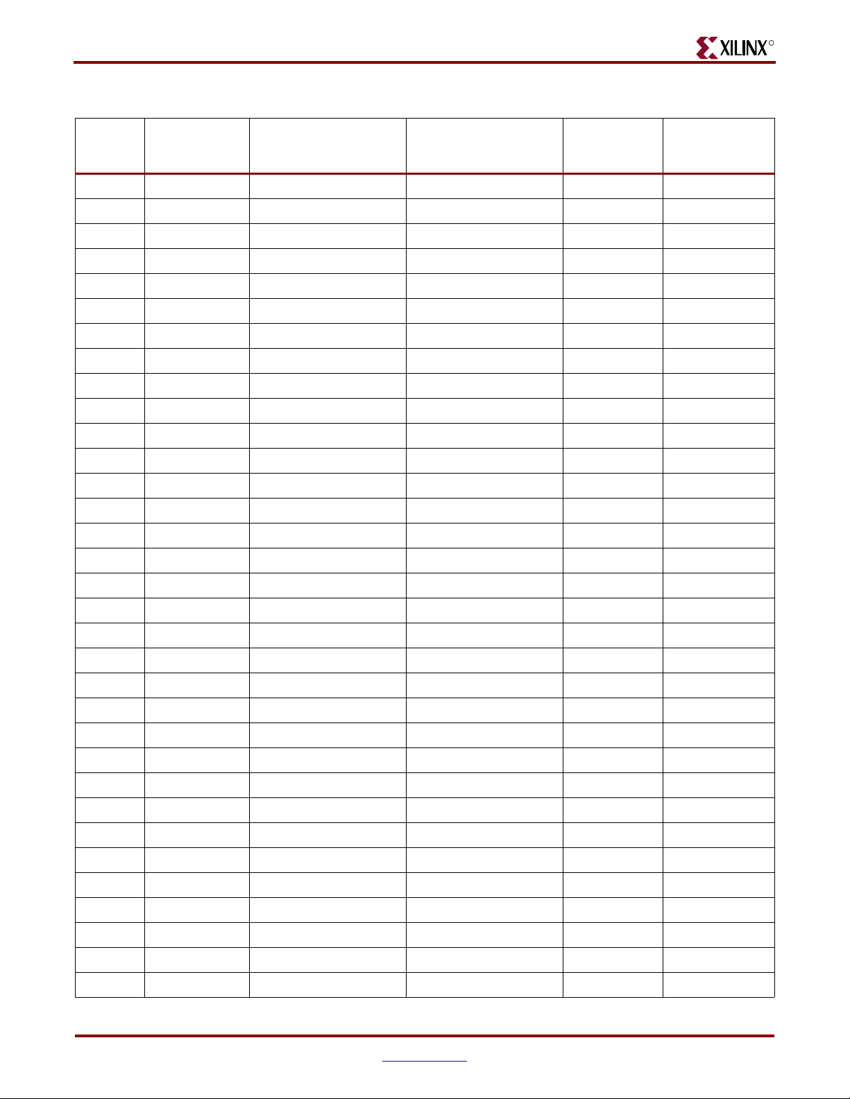
Table B-1: FPGA Pinout (Cont’d)
R
Pin
Numbers
Virtex-II Pro
Bank Number
Package
Functional Name
I/O Pin Names
Internal Script
Information
Package
Flight Times
(in microns)
D12 1 IO_L46N_1 top_address(9) 11050.72
D13 1 IO_L46P_1 top_address(10) 9988.1
G14 1 IO_L45N_1/VREF_1 Vref = 1.3V 7704.24
H14 1 IO_L45P_1 top_address(11) 6364.26
D10 1 IO_L44N_1 top_address(12) 13570.63
E10 1 IO_L44P_1 top_ba(0) 12296.5
E13 1 IO_L43N_1 top_ba(1) 8910.89
F13 1 IO_L43P_1 top_csb 7591.45
J14 1 IO_L39N_1 GND 4903.25
K14 1 IO_L39P_1 GND 5404.41
C9 1 IO_L38N_1 top_rasb 15339.71
D9 1 IO_L38P_1 top_casb 14631.43
G13 1 IO_L37N_1 top_web 5923
H13 1 IO_L37P_1 GND 4727.82
J12 1 IO_L09N_1/VREF_1 Vref = 1.3V 4323.64
K12 1 IO_L09P_1 top_rst_dqs_div_out 3066.04
D6 1 IO_L08N_1 top_rst_dqs_div_in 15105.89
D5 1 IO_L08P_1 GND 16085.61
E9 1 IO_L07N_1 PULLDOWN 10718.03
F9 1 IO_L07P_1 PULLDOWN 9223.77
J11 1 IO_L06N_1 PULLDOWN 4601.94
K11 1 IO_L06P_1 PULLDOWN 3344.34
J10 1 IO PULLDOWN 5273.75
G10 1 IO_L03N_1/VREF_1 Vref = 1.3V 6996.94
H10 1 IO_L03P_1 PULLDOWN 5691.71
G9 1 IO_L02N_1 PULLDOWN 7905.95
H9 1 IO_L02P_1 PULLDOWN 6327.18
E7 1 IO_L01N_1/VRP_1 Pulldown to GND for DCI 10150.32
E6 1 IO_L01P_1/VRN_1 Pullup to 2.6V for DCI 11097.26
D2 2 IO_L01N_2/VRP_2 Pulldown to GND for DCI 7113.13
D1 2 IO_L01P_2/VRN_2 Pullup to 2.6V for DCI 4624.16
F8 2 IO_L02N_2 ddr1_ckn0 3390.64
F7 2 IO_L02P_2 ddr1_ck0 5566.52
74 www.xilinx.com ML361 Virtex-II Pro Memory Board
UG060 (v1.2) November 8, 2007
Page 75

R
Table B-1: FPGA Pinout (Cont’d)
Pin
Numbers
Virtex-II Pro
Bank Number
Package
Functional Name
I/O Pin Names
Internal Script
Information
Package
Flight Times
(in microns)
E4 2 IO_L03N_2 ddr1_ckn1 6738.57
E3 2 IO_L03P_2 ddr1_ck1 14050.12
E2 2 IO_L04N_2/VREF_2 Vref = 1.3V 15547.77
E1 2 IO_L04P_2 ddr1_dqs0 15132.61
J8 2 IO_L05N_2 ddr1_dm3 6469.14
J7 2 IO_L05P_2 ddr1_dm4 7292.33
F5 2 IO_L06N_2 ddr1_dq0 10666.81
F4 2 IO_L06P_2 ddr1_dq1 11858.77
H2 2 IO_L31N_2 ddr1_dq2 12137.04
H1 2 IO_L31P_2 ddr1_dq3 13451.41
M10 2 IO_L32N_2 ddr1_dq4 3062.48
M9 2 IO_L32P_2 ddr1_dq5 4123.3
K5 2 IO_L33N_2 ddr1_dq6 8267.43
K4 2 IO_L33P_2 ddr1_dq7 9537.04
J2 2 IO_L34N_2/VREF_2 Vref = 1.3V no pin0 12149.07
K2 2 IO_L34P_2 ddr1_dm0 11352.59
L8 2 IO_L35N_2 ddr1_dm1 5592.79
L7 2 IO_L35P_2 ddr1_dm2 6793.53
L6 2 IO_L36N_2 ddr1_rst_dqs_div_in 7367.37
L5 2 IO_L36P_2 ddr1_rst_dqs_div_out 8143.52
K1 2 IO_L37N_2 PULLDOWN 12423.45
L1 2 IO_L37P_2 ddr1_dqs1 12451.17
N10 2 IO_L38N_2 PULLDOWN 2788.42
N9 2 IO_L38P_2 PULLDOWN 3972.59
M7 2 IO_L39N_2 ddr1_dq8 5610.09
M6 2 IO_L39P_2 ddr1_dq9 6975.04
L2 2 IO_L40N_2/VREF_2 Vref = 1.3V 11195.56
M2 2 IO_L40P_2 ddr1_dq10 12186.54
N8 2 IO_L41N_2 ddr1_dq11 4920.17
N7 2 IO_L41P_2 ddr1_dq12 6104.35
L4 2 IO_L42N_2 ddr1_dq13 9001.57
L3 2 IO_L42P_2 ddr1_dq14 10259.17
M4 2 IO_L43N_2 ddr1_dq15 8536.05
ML361 Virtex-II Pro Memory Board www.xilinx.com 75
UG060 (v1.2) November 8, 2007
Page 76

Table B-1: FPGA Pinout (Cont’d)
R
Pin
Numbers
Virtex-II Pro
Bank Number
Package
Functional Name
I/O Pin Names
Internal Script
Information
Package
Flight Times
(in microns)
M3 2 IO_L43P_2 PULLDOWN 9772.91
P10 2 IO_L44N_2 PULLDOWN 2638.82
P9 2 IO_L44P_2 PULLDOWN 3823
N6 2 IO_L45N_2 ddr1_ckn2 no_pin1 6306.01
N5 2 IO_L45P_2 ddr1_ck2 7563.61
M1 2 IO_L46N_2/VREF_2 Vref = 1.3V 11667.8
N1 2 IO_L46P_2 ddr1_dqs2 11804.99
P8 2 IO_L47N_2 GND 4770.58
P7 2 IO_L47P_2 GND 5954.75
N4 2 IO_L48N_2 ddr1_dq16 8437.77
N3 2 IO_L48P_2 ddr1_dq17 9778.21
N2 2 IO_L49N_2 ddr1_dq18 10426.76
P2 2 IO_L49P_2 ddr1_dq19 10530.82
R10 2 IO_L50N_2 ddr1_dq20 2488.12
R9 2 IO_L50P_2 ddr1_dq21 3672.29
P6 2 IO_L51N_2 ddr1_dq22 6499.99
P5 2 IO_L51P_2 ddr1_dq23 7603.44
P4 2 IO_L52N_2/VREF_2 Vref = 1.3V no_pin2 8102.88
P3 2 IO_L52P_2 ddr1_rasn 9339.48
T11 2 IO_L53N_2 ddr1_casn 1247.81
U11 2 IO_L53P_2 ddr1_wen 1919.47
R7 2 IO_L54N_2 ddr1_cke 4872.84
R6 2 IO_L54P_2 ddr1_csn 6425.42
P1 2 IO_L55N_2 GND 11291.77
R1 2 IO_L55P_2 ddr1_dqs3 11455.67
T10 2 IO_L56N_2 PULLDOWN 2752.93
T9 2 IO_L56P_2 PULLDOWN 3871.63
R4 2 IO_L57N_2 ddr1_dq24 8013.89
R3 2 IO_L57P_2 ddr1_dq25 9271.49
R2 2 IO_L58N_2/VREF_2 Vref = 1.3V 9961.47
T2 2 IO_L58P_2 ddr1_dq26 10173.21
T8 2 IO_L59N_2 ddr1_dq27 4753.73
T7 2 IO_L59P_2 ddr1_dq28 5872.43
76 www.xilinx.com ML361 Virtex-II Pro Memory Board
UG060 (v1.2) November 8, 2007
Page 77

R
Table B-1: FPGA Pinout (Cont’d)
Pin
Numbers
Virtex-II Pro
Bank Number
Package
Functional Name
I/O Pin Names
Internal Script
Information
Package
Flight Times
(in microns)
T6 2 IO_L60N_2 ddr1_dq29 6031.43
T5 2 IO_L60P_2 ddr1_dq30 7055.3
T4 2 IO_L85N_2 ddr1_dq31 7724.5
T3 2 IO_L85P_2 GND 9056.44
U10 2 IO_L86N_2 ddr1_ba0 2340.31
U9 2 IO_L86P_2 ddr1_ba1 3459.01
U6 2 IO_L87N_2 ddr1_a0 no_pin3 5801.93
U5 2 IO_L87P_2 ddr1_a1 6851.4
U2 2 IO_L88N_2/VREF_2 Vref = 1.3V 9665.64
V2 2 IO_L88P_2 ddr1_dqs4 10394.2
U8 2 IO_L89N_2 GND 4393.22
U7 2 IO_L89P_2 GND 5511.92
U4 2 IO_L90N_2 ddr1_dq32 7649.57
U3 2 IO_L90P_2 ddr1_dq33 8839.91
V3 3 IO_L90N_3 ddr1_dq34 8537.7
V4 3 IO_L90P_3 ddr1_dq35 7799.59
V7 3 IO_L89N_3 ddr1_dq36 5407.06
V8 3 IO_L89P_3 ddr1_dq37 4483.54
V5 3 IO_L88N_3 ddr1_dq38 6547.9
V6 3 IO_L88P_3 ddr1_dq39 5998.02
W2 3 IO_L87N_3/VREF_3 Vref = 1.3V no_pin4 9812.03
Y2 3 IO_L87P_3 ddr1_a2 10611.96
V9 3 IO_L86N_3 GND 3327.27
V10 3 IO_L86P_3 ddr1_dqs5 2405.17
W3 3 IO_L85N_3 GND 8919.9
W4 3 IO_L85P_3 GND 8159.47
Y1 3 IO_L60N_3 ddr1_dq40 11148.48
AA1 3 IO_L60P_3 ddr1_dq41 11691.6
V11 3 IO_L59N_3 ddr1_dq42 1638.53
W11 3 IO_L59P_3 ddr1_dq43 1610.19
W5 3 IO_L58N_3 ddr1_dq44 6678.99
W6 3 IO_L58P_3 ddr1_dq45 5936.59
Y3 3 IO_L57N_3/VREF_3 Vref = 1.3V 8909.69
ML361 Virtex-II Pro Memory Board www.xilinx.com 77
UG060 (v1.2) November 8, 2007
Page 78

Table B-1: FPGA Pinout (Cont’d)
R
Pin
Numbers
Virtex-II Pro
Bank Number
Package
Functional Name
I/O Pin Names
Internal Script
Information
Package
Flight Times
(in microns)
Y4 3 IO_L57P_3 ddr1_dq46 8145.63
W7 3 IO_L56N_3 ddr1_dq47 5773.96
W8 3 IO_L56P_3 ddr1_dm5 4826.38
Y6 3 IO_L55N_3 ddr1_a3 5961.45
Y7 3 IO_L55P_3 ddr1_a4 5219.05
AA2 3 IO_L54N_3 ddr1_a5 no_pin5 10317.88
AB2 3 IO_L54P_3 ddr1_a6 11488.21
W9 3 IO_L53N_3 GND 3619.48
W10 3 IO_L53P_3 ddr1_dqs6 2590.48
AA3 3 IO_L52N_3 GND 9502.86
AA4 3 IO_L52P_3 GND 8801.88
AB1 3 IO_L51N_3/VREF_3 Vref = 1.3V 12006.27
AC1 3 IO_L51P_3 ddr1_dq48 12342.28
Y9 3 IO_L50N_3 ddr1_dq49 3554
Y10 3 IO_L50P_3 ddr1_dq50 2606.42
AA5 3 IO_L49N_3 ddr1_dq51 7683.23
AA6 3 IO_L49P_3 ddr1_dq52 7555.89
AB3 3 IO_L48N_3 ddr1_dq53 9319.47
AB4 3 IO_L48P_3 ddr1_dq54 8556.07
AA7 3 IO_L47N_3 ddr1_dq55 5836.46
AA8 3 IO_L47P_3 ddr1_dm6 4888.88
AB5 3 IO_L46N_3 ddr1_a7 7371.9
AB6 3 IO_L46P_3 ddr1_a8 6629.5
AC2 3 IO_L45N_3/VREF_3 Vref = 1.3V no_pin6 10601.93
AD2 3 IO_L45P_3 ddr1_a9 11866.32
AA9 3 IO_L44N_3 PULLDOWN 3704.71
AA10 3 IO_L44P_3 ddr1_dqs7 2717.14
AC3 3 IO_L43N_3 PULLDOWN 9702.33
AC4 3 IO_L43P_3 PULLDOWN 8911.96
AD1 3 IO_L42N_3 ddr1_dq56 12256.07
AE1 3 IO_L42P_3 ddr1_dq57 12534.09
AB7 3 IO_L41N_3 ddr1_dq58 5986.05
AB8 3 IO_L41P_3 ddr1_dq59 5038.48
78 www.xilinx.com ML361 Virtex-II Pro Memory Board
UG060 (v1.2) November 8, 2007
Page 79

R
Table B-1: FPGA Pinout (Cont’d)
Pin
Numbers
Virtex-II Pro
Bank Number
Package
Functional Name
I/O Pin Names
Internal Script
Information
Package
Flight Times
(in microns)
AC6 3 IO_L40N_3 ddr1_dq60 6521.49
AC7 3 IO_L40P_3 ddr1_dq61 5779.09
AD3 3 IO_L39N_3/VREF_3 Vref = 1.3V 9751.53
AD4 3 IO_L39P_3 ddr1_dq62 9046.71
AB9 3 IO_L38N_3 ddr1_dq63 3854.3
AB10 3 IO_L38P_3 ddr1_dm7 2906.72
AD5 3 IO_L37N_3 ddr1_a10 8126.55
AD6 3 IO_L37P_3 ddr1_a11 8070.54
AE2 3 IO_L36N_3 ddr1_ckn3 no_pin7 11537.91
AF2 3 IO_L36P_3 ddr1_ck3 11948.48
AD7 3 IO_L35N_3 PULLDOWN 6675.24
AD8 3 IO_L35P_3 ddr1_dqs8 5651.11
AE4 3 IO_L34N_3 PULLDOWN 9342.05
AE5 3 IO_L34P_3 PULLDOWN 8811.79
AG1 3 IO_L33N_3/VREF_3 Vref = 1.3V 12986.31
AG2 3 IO_L33P_3 ddr1_dq64 12391.44
AC9 3 IO_L32N_3 ddr1_dq65 4005.01
AC10 3 IO_L32P_3 ddr1_dq66 3336.69
AF3 3 IO_L31N_3 ddr1_dq67 10624.52
AF4 3 IO_L31P_3 ddr1_dq68 10021.36
AL1 3 IO_L06N_3 ddr1_dq69 15821.97
AL2 3 IO_L06P_3 ddr1_dq70 15583.83
AG7 3 IO_L05N_3 ddr1_dq71 9638.17
AH8 3 IO_L05P_3 ddr1_dm8 9015.73
AH5 3 IO_L04N_3 ddr1_a12 9452.34
AH6 3 IO_L04P_3 PULLDOWN 9308.27
AK3 3 IO_L03N_3/VREF_3 Vref = 1.3V no_pin8 12802.28
AK4 3 IO_L03P_3 PULLDOWN 12761.57
AJ7 3 IO_L02N_3 ddr1_ckn4 12205.75
AJ8 3 IO_L02P_3 ddr1_ck4 10415.12
AJ4 3 IO_L01N_3/VRP_3 Pulldown to GND for DCI 11311.2
AJ5 3 IO_L01P_3/VRN_3 Pullup to 2.6V for DCI 10985.88
AL5 4 IO_L01N_4/DOUT GND 13235.56
ML361 Virtex-II Pro Memory Board www.xilinx.com 79
UG060 (v1.2) November 8, 2007
Page 80

Table B-1: FPGA Pinout (Cont’d)
R
Pin
Numbers
Virtex-II Pro
Bank Number
Package
Functional Name
I/O Pin Names
Internal Script
Information
Package
Flight Times
(in microns)
AL6 4 IO_L01P_4/INIT_B INITn 12205.78
AG9 4 IO_L02N_4/D0 FPGA.DO 6285.75
AH9 4 IO_L02P_4/D1 GND 7853.38
AK6 4 IO_L03N_4/D2 GND 11359.7
AK7 4 IO_L03P_4/D3 GND 11413.02
AF10 4 IO GND 5273.75
AL7 4 IO_L06N_4/VRP_4 M1_even_clk 12583.91
AM7 4 IO_L06P_4/VRN_4 M1_even_ D15 13750.42
AE11 4 IO_L07N_4 M1_even_ D14 3596.07
AF11 4 IO_L07P_4/VREF_4 M1_even_ D13 4532.67
AG10 4 IO_L08N_4 M1_even_ D12 7946.43
AH10 4 IO_L08P_4 M1_even_ D11 8820.26
AK8 4 IO_L09N_4 M1_even_ D10 11291.37
AL8 4 IO_L09P_4/VREF_4 M1_even_D9 11372.97
AE13 4 IO_L37N_4 M1_even_D8 2723.68
AF13 4 IO_L37P_4 M1_even_D7 3918.86
AG13 4 IO_L38N_4 M1_even_D6 8007.13
AH13 4 IO_L38P_4 M1_even_D5 8774.61
AJ11 4 IO_L39N_4 M1_even_D4 8630.23
AK11 4 IO_L39P_4 M1_even_D3 9736.03
AE14 4 IO_L43N_4 M1_even_D2 3696.3
AF14 4 IO_L43P_4 M1_even_D1 5289.64
AJ13 4 IO_L44N_4 M1_even_D0 9198.92
AK13 4 IO_L44P_4 M1_odd_clk 10605.95
AL11 4 IO_L45N_4 M1_odd_D15 10900.17
AM11 4 IO_L45P_4/VREF_4 M1_odd_D14 12224.04
AE15 4 IO_L46N_4 M1_odd_D13 3132.45
AF15 4 IO_L46P_4 M1_odd_D12 3969.05
AG14 4 IO_L47N_4 M1_odd_D11 8129.77
AH14 4 IO_L47P_4 M1_odd_D10 9100.75
AL13 4 IO_L48N_4 M1_odd_D9 9870.11
AL12 4 IO_L48P_4 M1_odd_D8 11409.38
AD16 4 IO_L49N_4 M1_odd_D7 2710.75
80 www.xilinx.com ML361 Virtex-II Pro Memory Board
UG060 (v1.2) November 8, 2007
Page 81

R
Table B-1: FPGA Pinout (Cont’d)
Pin
Numbers
Virtex-II Pro
Bank Number
Package
Functional Name
I/O Pin Names
Internal Script
Information
Package
Flight Times
(in microns)
AE16 4 IO_L49P_4 M1_odd_D6 3442.92
AJ14 4 IO GND 8953.05
AK14 4 IO GND 9556.17
AM14 4 IO_L54N_4 M1_odd_D5 12003.32
AM13 4 IO_L54P_4 M1_odd_D4 12348.43
AF16 4 IO_L55N_4 M1_odd_D3 3887.4
AG16 4 IO_L55P_4 M1_odd_D2 4909.89
AH15 4 IO_L56N_4 M1_odd_D1 7000
AJ15 4 IO_L56P_4 M1_odd_D0 8217.31
AL14 4 IO_L57N_4 GND 10563
AL15 4 IO_L57P_4/VREF_4 GND 10160.18
AD17 4 IO_L67N_4 GND 2503.07
AE17 4 IO_L67P_4 GND 3464.19
AH16 4 IO_L68N_4 GND 7362.9
AJ16 4 IO_L68P_4 GND 9128.85
AK16 4 IO_L69N_4 GND 9447.56
AL16 4 IO_L69P_4/VREF_4 GND 10269.32
AF17 4 IO_L73N_4 GND
AG17 4 IO_L73P_4 GND
AH17 4 IO_L74N_4/GCLK3S GND
AJ17 4 IO_L74P_4/GCLK2P GND
AK17 4 IO_L75N_4/GCLK1S GND
AL17 4 IO_L75P_4/GCLK0P GND
AL18 5 IO_L75N_5/GCLK7S CLK.SMAN
AK18 5 IO_L75P_5/GCLK6P CLK.SMAP
AJ18 5 IO_L74N_5/GCLK5S GND
AH18 5 IO_L74P_5/GCLK4P GND
AG18 5 IO_L73N_5 GND
AF18 5 IO_L73P_5 GND
AL19 5 IO_L69N_5/VREF_5 GND
AK19 5 IO_L69P_5 GND
AJ19 5 IO_L68N_5 GND
AH19 5 IO_L68P_5 GND
ML361 Virtex-II Pro Memory Board www.xilinx.com 81
UG060 (v1.2) November 8, 2007
Page 82

Table B-1: FPGA Pinout (Cont’d)
R
Pin
Numbers
Virtex-II Pro
Bank Number
Package
Functional Name
I/O Pin Names
Internal Script
Information
Package
Flight Times
(in microns)
AE18 5 IO_L67N_5 GND
AD18 5 IO_L67P_5 M2_even_clk
AL20 5 IO_L57N_5/VREF_5 M2_even_ D15
AL21 5 IO_L57P_5 M2_even_ D14
AJ20 5 IO_L56N_5 M2_even_ D13
AH20 5 IO_L56P_5 M2_even_ D12
AG19 5 IO_L55N_5 M2_even_ D11
AF19 5 IO_L55P_5 M2_even_ D10
AM22 5 IO_L54N_5 M2_even_D9
AM21 5 IO_L54P_5 M2_even_D8
AK21 5 IO GND
AJ21 5 IO GND
AE19 5 IO_L49N_5 M2_even_D7
AD19 5 IO_L49P_5 M2_even_D6
AL23 5 IO_L48N_5 M2_even_D5 11409.38
AL22 5 IO_L48P_5 M2_even_D4 9870.11
AH21 5 IO_L47N_5 M2_even_D3 9029.19
AG21 5 IO_L47P_5 M2_even_D2 8186.49
AF20 5 IO_L46N_5 M2_even_D1 3969.05
AE20 5 IO_L46P_5 M2_even_D0 3132.45
AM24 5 IO_L45N_5/VREF_5 M2_odd_clk 12224.04
AL24 5 IO_L45P_5 M2_odd_D15 10900.17
AK22 5 IO_L44N_5 M2_odd_D14 10795.23
AJ22 5 IO_L44P_5 M2_odd_D13 9429.62
AF21 5 IO_L43N_5 M2_odd_D12 5289.64
AE21 5 IO_L43P_5 M2_odd_D11 3696.3
AK24 5 IO_L39N_5 M2_odd_D10 9736.03
AJ24 5 IO_L39P_5 M2_odd_D9 8630.23
AH22 5 IO_L38N_5 M2_odd_D8 8786.32
AG22 5 IO_L38P_5 M2_odd_D7 8056.83
AF22 5 IO_L37N_5 M2_odd_D6 3918.86
AE22 5 IO_L37P_5 M2_odd_D5 2723.68
AL27 5 IO_L09N_5/VREF_5 M2_odd_D4 11372.97
82 www.xilinx.com ML361 Virtex-II Pro Memory Board
UG060 (v1.2) November 8, 2007
Page 83

R
Table B-1: FPGA Pinout (Cont’d)
Pin
Numbers
Virtex-II Pro
Bank Number
Package
Functional Name
I/O Pin Names
Internal Script
Information
Package
Flight Times
(in microns)
AK27 5 IO_L09P_5 M2_odd_D3 11420.7
AH25 5 IO_L08N_5 M2_odd_D2 8344.01
AG25 5 IO_L08P_5 M2_odd_D1 7652.81
AF24 5 IO_L07N_5/VREF_5 M2_odd_D0 4532.67
AE24 5 IO_L07P_5 GND 3596.07
AM28 5 IO_L06N_5/VRP_5 GND 13858.11
AL28 5 IO_L06P_5/VRN_5 GND 12527.75
AF25 5 IO GND
AK28 5 IO_L03N_5/D4 GND
AK29 5 IO_L03P_5/D5 GND
AH26 5 IO_L02N_5/D6 GND
AG26 5 IO_L02P_5/D7 GND
AL29 5 IO_L01N_5/RDWR_B PUSH1
AL30 5 IO_L01P_5/CS_B PUSH2
AJ30 6 IO_L01P_6/VRN_6 Pullup to 2.6V for DCI 10985.88
AJ31 6 IO_L01N_6/VRP_6 Pulldown to GND for DCI 11321.01
AJ27 6 IO_L02P_6 dimm_dm0 10529.58
AJ28 6 IO_L02N_6 dimm_dm1 11720.34
AK31 6 IO_L03P_6 dimm_dqs0 12761.57
AK32 6 IO_L03N_6/VREF_6 Vref = 1.3V 12802.28
AH29 6 IO_L04P_6 dimm_dq0 9308.27
AH30 6 IO_L04N_6 dimm_dq1 9452.34
AH27 6 IO_L05P_6 dimm_dq2 8891.47
AG28 6 IO_L05N_6 dimm_dq3 9638.17
AL33 6 IO_L06P_6 dimm_dq4 15583.83
AL34 6 IO_L06N_6 dimm_dq5 15821.97
AF31 6 IO_L31P_6 dimm_dq6 10021.36
AF32 6 IO_L31N_6 dimm_dq7 10624.52
AC25 6 IO_L32P_6 dimm_dm2 3336.69
AC26 6 IO_L32N_6 dimm_dm3 4005.01
AG33 6 IO_L33P_6 dimm_dm4 no_pin0 12391.44
AG34 6 IO_L33N_6/VREF_6 Vref = 1.3V 12986.31
AE30 6 IO_L34P_6 PULLDOWN 8811.79
ML361 Virtex-II Pro Memory Board www.xilinx.com 83
UG060 (v1.2) November 8, 2007
Page 84

Table B-1: FPGA Pinout (Cont’d)
R
Pin
Numbers
Virtex-II Pro
Bank Number
Package
Functional Name
I/O Pin Names
Internal Script
Information
Package
Flight Times
(in microns)
AE31 6 IO_L34N_6 PULLDOWN 9342.05
AD27 6 IO_L35P_6 dimm_dqs1 5651.11
AD28 6 IO_L35N_6 PULLDOWN 6675.24
AF33 6 IO_L36P_6 dimm_dq8 11948.48
AE33 6 IO_L36N_6 dimm_dq9 11537.91
AD29 6 IO_L37P_6 dimm_dq10 8070.54
AD30 6 IO_L37N_6 dimm_dq11 8126.55
AB25 6 IO_L38P_6 dimm_dq12 2906.72
AB26 6 IO_L38N_6 dimm_dq13 3854.3
AD31 6 IO_L39P_6 dimm_dq14 9046.71
AD32 6 IO_L39N_6/VREF_6 Vref = 1.3V 9751.53
AC28 6 IO_L40P_6 dimm_dq15 5779.09
AC29 6 IO_L40N_6 dimm_dm5 6521.49
AB27 6 IO_L41P_6 dimm_dm6 5038.48
AB28 6 IO_L41N_6 dimm_dm7 5986.05
AE34 6 IO_L42P_6 dimm_dm8 no_pin1 12534.09
AD34 6 IO_L42N_6 dimm_sda 12256.07
AC31 6 IO_L43P_6 PULLDOWN 8911.96
AC32 6 IO_L43N_6 GND 9702.33
AA25 6 IO_L44P_6 dimm_dqs2 2717.14
AA26 6 IO_L44N_6 GND 3704.71
AD33 6 IO_L45P_6 dimm_dq16 11866.32
AC33 6 IO_L45N_6/VREF_6 Vref = 1.3V 10601.93
AB29 6 IO_L46P_6 dimm_dq17 6629.5
AB30 6 IO_L46N_6 dimm_dq18 7371.9
AA27 6 IO_L47P_6 dimm_dq19 4888.88
AA28 6 IO_L47N_6 dimm_dq20 5836.46
AB31 6 IO_L48P_6 dimm_dq21 8556.07
AB32 6 IO_L48N_6 dimm_dq22 9319.47
AA29 6 IO_L49P_6 dimm_dq23 7555.89
AA30 6 IO_L49N_6 PULLDOWN 7683.23
Y25 6 IO_L50P_6 dimm_ck0 2606.42
Y26 6 IO_L50N_6 dimm_ckn0 3554
84 www.xilinx.com ML361 Virtex-II Pro Memory Board
UG060 (v1.2) November 8, 2007
Page 85

R
Table B-1: FPGA Pinout (Cont’d)
Pin
Numbers
Virtex-II Pro
Bank Number
Package
Functional Name
I/O Pin Names
Internal Script
Information
Package
Flight Times
(in microns)
AC34 6 IO_L51P_6 PULLDOWN no_pin2 12342.28
AB34 6 IO_L51N_6/VREF_6 Vref = 1.3V 12006.27
AA31 6 IO_L52P_6 PULLDOWN 8801.88
AA32 6 IO_L52N_6 PULLDOWN 9502.86
W25 6 IO_L53P_6 dimm_dqs3 2590.48
W26 6 IO_L53N_6 GND 3619.48
AB33 6 IO_L54P_6 dimm_dq24 11488.21
AA33 6 IO_L54N_6 dimm_dq25 10317.88
Y28 6 IO_L55P_6 dimm_dq26 5219.05
Y29 6 IO_L55N_6 dimm_dq27 5961.45
W27 6 IO_L56P_6 dimm_dq28 4826.38
W28 6 IO_L56N_6 dimm_dq29 5773.96
Y31 6 IO_L57P_6 dimm_dq30 8145.63
Y32 6 IO_L57N_6/VREF_6 Vref = 1.3V 8909.69
W29 6 IO_L58P_6 dimm_dq31 5936.59
W30 6 IO_L58N_6 GND 6678.99
W24 6 IO_L59P_6 dimm_ck1 1610.19
V24 6 IO_L59N_6 dimm_ckn1 1638.53
AA34 6 IO_L60P_6 dimm_ck2 no_pin3 11691.6
Y34 6 IO_L60N_6 dimm_ckn2 11148.48
W31 6 IO_L85P_6 dimm_s0N 8159.47
W32 6 IO_L85N_6 dimm_s1N 8919.9
V25 6 IO_L86P_6 dimm_dqs4 2405.17
V26 6 IO_L86N_6 GND 3327.27
Y33 6 IO_L87P_6 dimm_dq32 10611.96
W33 6 IO_L87N_6/VREF_6 Vref = 1.3V 9812.03
V29 6 IO_L88P_6 dimm_dq33 5998.02
V30 6 IO_L88N_6 dimm_dq34 6547.9
V27 6 IO_L89P_6 dimm_dq35 4483.54
V28 6 IO_L89N_6 dimm_dq36 5407.06
V31 6 IO_L90P_6 dimm_dq37 7799.59
V32 6 IO_L90N_6 dimm_dq38 8537.7
U32 7 IO_L90P_7 dimm_dq39 8839.91
ML361 Virtex-II Pro Memory Board www.xilinx.com 85
UG060 (v1.2) November 8, 2007
Page 86

Table B-1: FPGA Pinout (Cont’d)
R
Pin
Numbers
Virtex-II Pro
Bank Number
Package
Functional Name
I/O Pin Names
Internal Script
Information
Package
Flight Times
(in microns)
U31 7 IO_L90N_7 PULLDOWN 7626.14
U28 7 IO_L89P_7 dimm_rasN no_pin4 5511.92
U27 7 IO_L89N_7 dimm_casN 4393.22
V33 7 IO_L88P_7 dimm_weN 10394.2
U33 7 IO_L88N_7/VREF_7 Vref = 1.3V 9665.64
U30 7 IO_L87P_7 dimm_rst_dqs_div_out 6851.4
U29 7 IO_L87N_7 dimm_rst_dqs_div_in 5801.93
U26 7 IO_L86P_7 PULLDOWN 3459.01
U25 7 IO_L86N_7 PULLDOWN 2340.31
T32 7 IO_L85P_7 dimm_dqs5 9056.44
T31 7 IO_L85N_7 PULLDOWN 7724.5
T30 7 IO_L60P_7 dimm_dq40 7055.3
T29 7 IO_L60N_7 dimm_dq41 6031.43
T28 7 IO_L59P_7 dimm_dq42 5872.43
T27 7 IO_L59N_7 dimm_dq43 4753.73
T33 7 IO_L58P_7 dimm_dq44 10173.21
R33 7 IO_L58N_7/VREF_7 Vref = 1.3V 9961.47
R32 7 IO_L57P_7 dimm_dq45 9271.49
R31 7 IO_L57N_7 dimm_dq46 8013.89
T26 7 IO_L56P_7 dimm_dq47 3871.63
T25 7 IO_L56N_7 GND 2752.93
R34 7 IO_L55P_7 dimm_cke0 11455.67
P34 7 IO_L55N_7 dimm_cke1 11291.77
R29 7 IO_L54P_7 dimm_ba0 no_pin5 6425.42
R28 7 IO_L54N_7 dimm_ba1 4872.84
U24 7 IO_L53P_7 GND 1919.47
T24 7 IO_L53N_7 GND 1247.81
P32 7 IO_L52P_7 dimm_dqs6 9339.48
P31 7 IO_L52N_7/VREF_7 Vref = 1.3V 8102.88
P30 7 IO_L51P_7 dimm_dq48 7603.44
P29 7 IO_L51N_7 dimm_dq49 6499.99
R26 7 IO_L50P_7 dimm_dq50 3672.29
R25 7 IO_L50N_7 dimm_dq51 2488.12
86 www.xilinx.com ML361 Virtex-II Pro Memory Board
UG060 (v1.2) November 8, 2007
Page 87

R
Table B-1: FPGA Pinout (Cont’d)
Pin
Numbers
Virtex-II Pro
Bank Number
Package
Functional Name
I/O Pin Names
Internal Script
Information
Package
Flight Times
(in microns)
P33 7 IO_L49P_7 dimm_dq52 10530.82
N33 7 IO_L49N_7 dimm_dq53 10426.76
N32 7 IO_L48P_7 dimm_dq54 9778.21
N31 7 IO_L48N_7 dimm_dq55 8437.77
P28 7 IO_L47P_7 dimm_a0 no_pin6 5954.75
P27 7 IO_L47N_7 dimm_a1 4770.58
N34 7 IO_L46P_7 dimm_a2 11804.99
M34 7 IO_L46N_7/VREF_7 Vref = 1.3V 11667.8
N30 7 IO_L45P_7 dimm_a3 7563.61
N29 7 IO_L45N_7 dimm_a4 6306.01
P26 7 IO_L44P_7 PULLDOWN 3823
P25 7 IO_L44N_7 PULLDOWN 2638.82
M32 7 IO_L43P_7 dimm_dqs7 9772.91
M31 7 IO_L43N_7 PULLDOWN 8536.05
L32 7 IO_L42P_7 dimm_dq56 10259.17
L31 7 IO_L42N_7 dimm_dq57 9001.57
N28 7 IO_L41P_7 dimm_dq58 6104.35
N27 7 IO_L41N_7 dimm_dq59 4920.17
M33 7 IO_L40P_7 dimm_dq60 12186.54
L33 7 IO_L40N_7/VREF_7 Vref = 1.3V 11195.56
M29 7 IO_L39P_7 dimm_dq61 6975.04
M28 7 IO_L39N_7 dimm_dq62 5610.09
N26 7 IO_L38P_7 dimm_dq63 3972.59
N25 7 IO_L38N_7 PULLDOWN 2788.42
L34 7 IO_L37P_7 dimm_a6 12451.17
K34 7 IO_L37N_7 dimm_a7 12423.45
L30 7 IO_L36P_7 dimm_a8 no_pin7 8143.52
L29 7 IO_L36N_7 dimm_a9 7340.48
L28 7 IO_L35P_7 dimm_a5 6793.53
L27 7 IO_L35N_7 GND 5592.79
K33 7 IO_L34P_7 dimm_dqs8 11352.59
J33 7 IO_L34N_7/VREF_7 Vref = 1.3V 12123.95
K31 7 IO_L33P_7 dimm_dq64 9537.04
ML361 Virtex-II Pro Memory Board www.xilinx.com 87
UG060 (v1.2) November 8, 2007
Page 88

Table B-1: FPGA Pinout (Cont’d)
R
Pin
Numbers
Virtex-II Pro
Bank Number
Package
Functional Name
I/O Pin Names
Internal Script
Information
Package
Flight Times
(in microns)
K30 7 IO_L33N_7 dimm_dq65 8267.43
M26 7 IO_L32P_7 dimm_dq66 4123.3
M25 7 IO_L32N_7 dimm_dq67 3062.48
H34 7 IO_L31P_7 dimm_dq68 13451.41
H33 7 IO_L31N_7 dimm_dq69 12137.04
F31 7 IO_L06P_7 dimm_dq70 11858.77
F30 7 IO_L06N_7 dimm_dq71 10666.81
J28 7 IO_L05P_7 dimm_a10 no_pin8 7292.33
J27 7 IO_L05N_7 dimm_a11 6469.14
E34 7 IO_L04P_7 dimm_a12 15132.61
E33 7 IO_L04N_7/VREF_7 Vref = 1.3V 13663.12
E32 7 IO_L03P_7 dimm_sa0 13396.34
E31 7 IO_L03N_7 dimm_sa1 11802.85
F28 7 IO_L02P_7 dimm_sa2 11146.23
F27 7 IO_L02N_7 dimm_scl 12438.46
D34 7 IO_L01P_7/VRN_7 Pullup to 2.6V for DCI 15547.77
D33 7 IO_L01N_7/VRP_7 Pulldown to GND for DCI 14050.12
J26 PROG_B PROGRAMn
K25 HSWAP_EN HSWAP
K26 DXP
G27 DXN
A29 TXNPAD4
A28 TXPPAD4
A27 RXPPAD4
A26 RXNPAD4
A21 TXNPAD6
A20 TXPPAD6
A19 RXPPAD6
A18 RXNPAD6
A17 TXNPAD7
A16 TXPPAD7
A15 RXPPAD7
A14 RXNPAD7
88 www.xilinx.com ML361 Virtex-II Pro Memory Board
UG060 (v1.2) November 8, 2007
Page 89

R
Table B-1: FPGA Pinout (Cont’d)
Pin
Numbers
Virtex-II Pro
Bank Number
Package
Functional Name
I/O Pin Names
A9 TXNPAD9
A8 TXPPAD9
A7 RXPPAD9
A6 RXNPAD9
G8 RSVD
K9 VBATT
K10 TMS TMS
J9 TCK TCK
H7 DO TDO.FPGA.to.TDO.PORT
AE9 CCLK FPGA.CCLK
AF9 PWRDWN_B PWRDWN
AE10 DONE DONE
AP6 RXNPAD16 RXNPAD18
AP7 RXPPAD16 RXPPAD18
Internal Script
Information
Package
Flight Times
(in microns)
AP8 TXPPAD16 TXPPAD18
AP9 TXNPAD16 TXNPAD18
AP14 RXNPAD18 RXNPAD18
AP15 RXPPAD18 RXPPAD18
AP16 TXPPAD18 TXPPAD18
AP17 TXNPAD18 TXNPAD18
AP18 RXNPAD19
AP19 RXPPAD19
AP20 TXPPAD19
AP21 TXNPAD19
AP26 RXNPAD21
AP27 RXPPAD21
AP28 TXPPAD21
AP29 TXNPAD21
AE25 M2 M2
AF26 M0 M0
AE26 M1 M1
H28 TDI TDO.PROM.to.TDI.FPGA
ML361 Virtex-II Pro Memory Board www.xilinx.com 89
UG060 (v1.2) November 8, 2007
Page 90

R
90 www.xilinx.com ML361 Virtex-II Pro Memory Board
UG060 (v1.2) November 8, 2007
 Loading...