

Page 1

LogiCORE IP
MicroBlaze Micro
Controller System v1.3
Product Guide
PG048 December 18, 2012
Page 2

Table of Contents
SECTION I: SUMMARY
IP Facts
Chapter 1: Overview
Feature Summary. . . . . . . . . . . . . . . . . . . . . . . . . . . . . . . . . . . . . . . . . . . . . . . . . . . . . . . . . . . . . . . . . . 5
Licensing and Ordering Information . . . . . . . . . . . . . . . . . . . . . . . . . . . . . . . . . . . . . . . . . . . . . . . . . . . 6
Chapter 2: Product Specification
Standards Compliance . . . . . . . . . . . . . . . . . . . . . . . . . . . . . . . . . . . . . . . . . . . . . . . . . . . . . . . . . . . . . . 7
Performance. . . . . . . . . . . . . . . . . . . . . . . . . . . . . . . . . . . . . . . . . . . . . . . . . . . . . . . . . . . . . . . . . . . . . . 7
Resource Utilization. . . . . . . . . . . . . . . . . . . . . . . . . . . . . . . . . . . . . . . . . . . . . . . . . . . . . . . . . . . . . . . . 8
Port Descriptions . . . . . . . . . . . . . . . . . . . . . . . . . . . . . . . . . . . . . . . . . . . . . . . . . . . . . . . . . . . . . . . . . . 9
Register Space . . . . . . . . . . . . . . . . . . . . . . . . . . . . . . . . . . . . . . . . . . . . . . . . . . . . . . . . . . . . . . . . . . . 10
Chapter 3: Designing with the Core
General Design Guidelines . . . . . . . . . . . . . . . . . . . . . . . . . . . . . . . . . . . . . . . . . . . . . . . . . . . . . . . . . 11
Clocking. . . . . . . . . . . . . . . . . . . . . . . . . . . . . . . . . . . . . . . . . . . . . . . . . . . . . . . . . . . . . . . . . . . . . . . . . 11
Resets . . . . . . . . . . . . . . . . . . . . . . . . . . . . . . . . . . . . . . . . . . . . . . . . . . . . . . . . . . . . . . . . . . . . . . . . . . 12
Protocol Description . . . . . . . . . . . . . . . . . . . . . . . . . . . . . . . . . . . . . . . . . . . . . . . . . . . . . . . . . . . . . . 12
SECTION II: VIVADO DESIGN SUITE
Chapter 4: Customizing and Generating the Core
GUI . . . . . . . . . . . . . . . . . . . . . . . . . . . . . . . . . . . . . . . . . . . . . . . . . . . . . . . . . . . . . . . . . . . . . . . . . . . . 14
Parameter Values. . . . . . . . . . . . . . . . . . . . . . . . . . . . . . . . . . . . . . . . . . . . . . . . . . . . . . . . . . . . . . . . . 22
Parameter - Port Dependencies . . . . . . . . . . . . . . . . . . . . . . . . . . . . . . . . . . . . . . . . . . . . . . . . . . . . . 28
Tool Flow . . . . . . . . . . . . . . . . . . . . . . . . . . . . . . . . . . . . . . . . . . . . . . . . . . . . . . . . . . . . . . . . . . . . . . . 29
Chapter 5: Constraining the Core
Required Constraints . . . . . . . . . . . . . . . . . . . . . . . . . . . . . . . . . . . . . . . . . . . . . . . . . . . . . . . . . . . . . . 32
MicroBlaze Micro Controller System v1.3 www.xilinx.com 1
PG048 December 18, 2012
Page 3

Device, Package, and Speed Grade Selections. . . . . . . . . . . . . . . . . . . . . . . . . . . . . . . . . . . . . . . . . . 32
Clock Frequencies . . . . . . . . . . . . . . . . . . . . . . . . . . . . . . . . . . . . . . . . . . . . . . . . . . . . . . . . . . . . . . . . 32
Clock Management . . . . . . . . . . . . . . . . . . . . . . . . . . . . . . . . . . . . . . . . . . . . . . . . . . . . . . . . . . . . . . . 32
Clock Placement. . . . . . . . . . . . . . . . . . . . . . . . . . . . . . . . . . . . . . . . . . . . . . . . . . . . . . . . . . . . . . . . . . 32
Banking . . . . . . . . . . . . . . . . . . . . . . . . . . . . . . . . . . . . . . . . . . . . . . . . . . . . . . . . . . . . . . . . . . . . . . . . . 32
Transceiver Placement . . . . . . . . . . . . . . . . . . . . . . . . . . . . . . . . . . . . . . . . . . . . . . . . . . . . . . . . . . . . 33
I/O Standard and Placement. . . . . . . . . . . . . . . . . . . . . . . . . . . . . . . . . . . . . . . . . . . . . . . . . . . . . . . . 33
SECTION III: ISE DESIGN SUITE
Chapter 6: Customizing and Generating the Core
GUI . . . . . . . . . . . . . . . . . . . . . . . . . . . . . . . . . . . . . . . . . . . . . . . . . . . . . . . . . . . . . . . . . . . . . . . . . . . . 35
Parameter Values. . . . . . . . . . . . . . . . . . . . . . . . . . . . . . . . . . . . . . . . . . . . . . . . . . . . . . . . . . . . . . . . . 43
Parameter - Port Dependencies . . . . . . . . . . . . . . . . . . . . . . . . . . . . . . . . . . . . . . . . . . . . . . . . . . . . . 43
Tool Flow . . . . . . . . . . . . . . . . . . . . . . . . . . . . . . . . . . . . . . . . . . . . . . . . . . . . . . . . . . . . . . . . . . . . . . . 43
Chapter 7: Constraining the Core
Clock Management . . . . . . . . . . . . . . . . . . . . . . . . . . . . . . . . . . . . . . . . . . . . . . . . . . . . . . . . . . . . . . . 51
SECTION IV: APPENDICES
Appendix A: Application Software Development
Xilinx Software Development Kit . . . . . . . . . . . . . . . . . . . . . . . . . . . . . . . . . . . . . . . . . . . . . . . . . . . . 53
Device Drivers . . . . . . . . . . . . . . . . . . . . . . . . . . . . . . . . . . . . . . . . . . . . . . . . . . . . . . . . . . . . . . . . . . . 53
Appendix B: Debugging
Finding Help on Xilinx.com . . . . . . . . . . . . . . . . . . . . . . . . . . . . . . . . . . . . . . . . . . . . . . . . . . . . . . . . . 54
Debug Tools . . . . . . . . . . . . . . . . . . . . . . . . . . . . . . . . . . . . . . . . . . . . . . . . . . . . . . . . . . . . . . . . . . . . . 56
Troubleshooting. . . . . . . . . . . . . . . . . . . . . . . . . . . . . . . . . . . . . . . . . . . . . . . . . . . . . . . . . . . . . . . . . . 56
Simulation Debug. . . . . . . . . . . . . . . . . . . . . . . . . . . . . . . . . . . . . . . . . . . . . . . . . . . . . . . . . . . . . . . . . 60
Hardware Debug . . . . . . . . . . . . . . . . . . . . . . . . . . . . . . . . . . . . . . . . . . . . . . . . . . . . . . . . . . . . . . . . . 61
Appendix C: Additional Resources
Xilinx Resources . . . . . . . . . . . . . . . . . . . . . . . . . . . . . . . . . . . . . . . . . . . . . . . . . . . . . . . . . . . . . . . . . . 62
References . . . . . . . . . . . . . . . . . . . . . . . . . . . . . . . . . . . . . . . . . . . . . . . . . . . . . . . . . . . . . . . . . . . . . . 62
Revision History . . . . . . . . . . . . . . . . . . . . . . . . . . . . . . . . . . . . . . . . . . . . . . . . . . . . . . . . . . . . . . . . . . 63
Notice of Disclaimer. . . . . . . . . . . . . . . . . . . . . . . . . . . . . . . . . . . . . . . . . . . . . . . . . . . . . . . . . . . . . . . 63
Automotive Applications Disclaimer . . . . . . . . . . . . . . . . . . . . . . . . . . . . . . . . . . . . . . . . . . . . . . . . . 63
MicroBlaze Micro Controller System v1.3 www.xilinx.com 2
PG048 December 18, 2012
Page 4

SECTION I: SUMMARY
IP Facts
Overview
Product Specification
Designing with the Core
MicroBlaze Micro Controller System v1.3 www.xilinx.com 3
PG048 December 18, 2012
Page 5

IP Facts
Introduction
The LogiCORE™ MicroBlaze™ Micro Controller
System (MCS) is a complete standalone
processor system intended for controller
applications. It is highly integrated and includes
the MicroBlaze processor, local memory for
program and data storage as well as a tightly
coupled I/O module implementing a standard
set of peripherals.
The MicroBlaze processor included in the MCS
has a fixed configuration, optimized for
minimal area. The full-featured MicroBlaze
processor is available in the ISE® Design Suite
Embedded Edition and the Vivado™ IP
integrator.
Features
• MicroBlaze processor
•Local Memory
• MicroBlaze Debug Module (MDM)
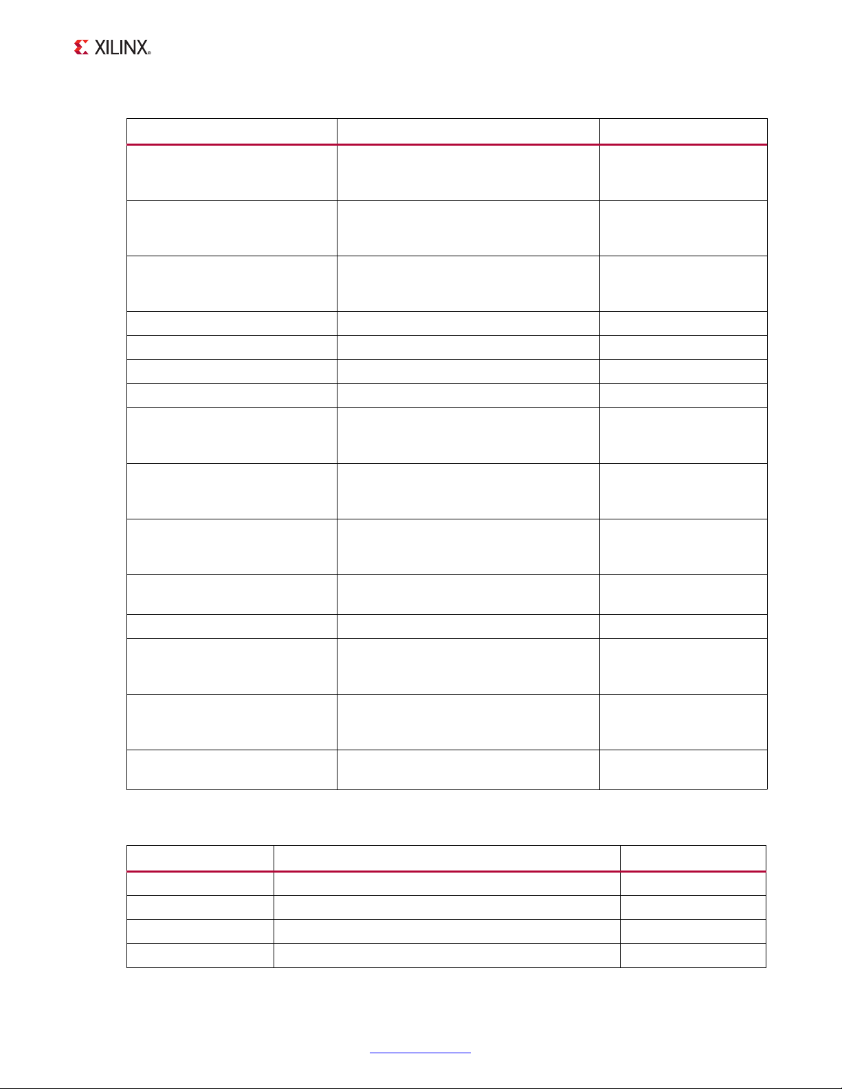
LogiCORE IP Facts Table
Core Specifics
Supported
Device Family
Supported User
Interfaces
Resources See Ta b le 2 -2 .
Zynq™-7000
(1)
(2)
, Virtex®-7, Kintex™-7, Artix™-7,
Virtex-6, Virtex-5, Spartan
Local Memory Bus (LMB), Dynamic
Reconfiguration Port (DRP)
®-6, Virtex-4,
Spartan-3
Provided with Core
Design Files
Example
Design
Test Bench Not Provided
Constraints File Not Provided
Simulation
Model
Supported
S/W Driver
Design Entry
Simulation
Synthesis
(3)
Tested Design Flows
Verilog and/or VHDL Structural
(4)
ISE Design Suite 14.4
Vivado Design Suite 2012.4
Mentor Graphics ModelSim
Xilinx Synthesis Technology (XST)
ISE: VHDL
Vivado: RTL
Not Provided
Standalone
Vivado Simulator
Vivado Synthesis
(5)
• Tightly Coupled I/O Module including
I/O Bus
°
Interrupt Controller using fast interrupt
°
mode
UART
°
Fixed Interval Timers
°
Programmable Interval Timers
°
General Purpose Inputs
°
General Purpose Outputs
°
Provided by Xilinx @ www.xilinx.com/support
Notes:
1. For a complete listing of supported devices, see the release
notes for this core.
2. Supported in ISE Design Suite implementations only.
3. Standalone driver details can be found in the EDK or SDK
directory (<install_directory>/doc/usenglish/
xilinx_drivers.htm). Linux OS and driver support information is
available from //wiki.xilinx.com
4. For the supported versions of the tools, see the Xilinx Design
Tools: Release Notes Guide.
5. Supports only 7 series devices.
Support
.
MicroBlaze Micro Controller System v1.3 www.xilinx.com 4
PG048 December 18, 2012 Product Specification
Page 6

Overview
ILMB
MicroBlaze
Local
Memory Bus
LMB BRAM
Interface Controller
Block RAM
(Dual Port)
DLMB
Local
Memory Bus
LMB BRAM
Interface Controller
I/O Module
MicroBlaze
Debug
Optional Feature
The MicroBlaze™ Micro Controller System (MCS) is highly integrated standalone processor
system intended for controller applications. Data and program is stored in a local memory,
debug is facilitated by the MicroBlaze Debug Module, MDM. A standard set of peripherals
is also included, providing basic functionality like interrupt controller, UART, timers and
general purpose input and outputs.
X-Ref Target - Figure 1-1
Chapter 1
MicroBlaze Micro Controller System v1.3 www.xilinx.com 5
PG048 December 18, 2012
Figure 1-1: MicroBlaze Micro Controller System (MCS)
Feature Summary
MicroBlaze
The MicroBlaze embedded processor soft core is a reduced instruction set computer (RISC)
optimized for implementation in Xilinx® Field Programmable Gate Arrays (FPGAs). Detailed
information on the MicroBlaze processor can be found in the MicroBlaze Processor
Reference Guide [Ref 5].
The MicroBlaze parameters in MicroBlaze MCS are fixed except for the possibility to enable/
disable the debug functionality. The values of all MicroBlaze parameters in MicroBlaze MCS
can be found in Tab le 4- 2. These values correspond to the MicroBlaze Configuration Wizard
Minimum Area configuration.
Page 7

Chapter 1: Overview
Local Memory
Local memory is used for data and program storage and is implemented using block RAM.
The size of the local memory is parameterized and can be between 4kB and 64kB. The local
memory is connected to MicroBlaze through the Local Memory Bus, LMB, and the LMB
BRAM Interface Controllers. Detailed information on LMB can be found in the Local Memory
Bus (LMB) V10 data sheet [Ref 1] and detailed information on the LMB BRAM Interface
Controller can be found in the LMB BRAM Interface Controller data sheet [Ref 2].
The LMB Bus and the LMB BRAM Interface Controller parameters are fixed except for the
memory size. The value of the parameters can be found in Tabl e 4 -4, Ta ble 4-5 , Tab le 4- 6
and Tab le 4- 7.
Debug
The MicroBlaze Debug Module, MDM, connects MicroBlaze debug logic to the XMD low
level debugger. XMD can be used for downloading software, to set break points, view
register and memory contents. Detailed information about MDM can be found in the
MicroBlaze Debug Module (MDM) data sheet [Ref 3].
The MDM parameters, except the JTAG user-defined register, are fixed and their values can
be found in Tab le 4- 8.
When more than one MicroBlaze MCS instance with debug enabled is included in the same
design, a unique JTAG register must be used for each instance. When a single instance is
used, the default value USER2 should be kept unchanged.
I/O Module
The I/O Module is a light-weight implementation of a set of standard I/O functions
commonly used in a MicroBlaze processor sub-system. Detailed information about the I/O
Module can be found in the I/O Module product guide [Ref 4].
The I/O Module registers are mapped at address 0x4000000, and the I/O Bus is mapped at
address 0xC0000000-0xFFFFFFFF in the MicroBlaze memory space. The fixed I/O Module
parameter values can be found in Tabl e 4-3 .
Licensing and Ordering Information
This Xilinx LogiCORE™ IP module is provided at no additional cost with the Xilinx Vivado™
Design Suite and ISE® Design Suite tools under the terms of the Xilinx End User License
Information about this and other Xilinx LogiCORE IP modules is available at the Xilinx
Intellectual Property page. For information about pricing and availability of other Xilinx
LogiCORE IP modules and tools, contact your local Xilinx sales representative
MicroBlaze Micro Controller System v1.3 www.xilinx.com 6
PG048 December 18, 2012
.
.
Page 8

Product Specification
Standards Compliance
The I/O Bus interface provided by the I/O Module is fully compatible with the Xilinx®
Dynamic Reconfiguration Port (DRP). For a detailed description of the DRP, see the 7 Series
FPGAs Configuration User Guide [Ref 10].
Performance
The frequency and latency of the modules in the MicroBlaze™ MCS are optimized for use
together with MicroBlaze. This means that the frequency targets are aligned to MicroBlaze
targets as well as the access latency optimized for MicroBlaze data access.
Chapter 2
Maximum Frequencies
The following are clock frequencies for the target families. The maximum achievable clock
frequency can vary. The maximum achievable clock frequency and all resource counts can
be affected by the used tool flow, other tool options, additional logic in the FPGA, using
different versions of Xilinx tools, and other factors.
Table 2-1: Maximum Frequencies
Architecture Speed grade Max Frequency
Spartan®-6 -4 195
Virtex®-6 -3 300
Artix™-7 -3 225
Kintex™-7 -3 320
Virtex-7 -3 320
Latency
Data read from I/O Module registers is available two clock cycles after the MicroBlaze load
instruction is executed.
MicroBlaze Micro Controller System v1.3 www.xilinx.com 7
PG048 December 18, 2012
Page 9

Chapter 2: Product Specification
Data write to I/O Module registers is performed the clock cycle after the MicroBlaze store
instruction is executed.
Data accesses to peripherals connected on the I/O Bus take three clock cycles plus the
number of wait states introduced by the accessed peripheral.
Throughput
The maximum throughput when using the I/O Bus is one read or write access every three
clock cycles.
Resource Utilization
Because the MicroBlaze MCS is a module that is used together with other parts of the
design in the FPGA, the utilization and timing numbers reported in this section are just
estimates, and the actual utilization of FPGA resources and timing of the MicroBlaze MCS
design will vary from the results reported here. All parameters not given in Tab le 2- 2 have
their default values.
Table 2-2:
Parameter Values (other parameters at default value) Device Resources
C_USE_UART_RX
11000 0 00000000 546 276
11150 0 00000000 606 340
1115165000 00000000 620 353
1115165000 1 32 000000 656 441
1115165000 1 32 1 32 0 0 0 0 658 473
1115165000 1 32 1 32 1 32 0 0 659 505
1115165000 1 32 1 32 1 32 1 0 675 610
1115165000 1 32 1 32 1 32 1 1 882 946
Performance and Resource Utilization Benchmarks on Virtex-6 (xc6vlx240t-1-ff1156)
LUTs Flip-Flops
C_USE_UART_TX
C_USE_FIT1
C_INTC_INTR_SIZE
C_INTC_USE_EXT_INTR
C_FIT1_No_CLOCKS
C_USE_PIT1
C_PIT1_SIZE
C_USE_GPI1
C_GPI1_SIZE
C_USE_GPO1
C_GPO1_SIZE
C_USE_IO_BUS
C_DEBUG_ENABLE
MicroBlaze Micro Controller System v1.3 www.xilinx.com 8
PG048 December 18, 2012
Page 10

Chapter 2: Product Specification
Port Descriptions
The I/O ports and signals for MicroBlaze MCS are listed and described in Tabl e 2- 3.
Table 2-3: MicroBlaze MCS Signals
Port Name MSB:LSB I/O Description
System Signals
Clk I System clock
Reset I System reset
MicroBlaze Signals
Trace_Valid_Instr O Valid instruction on trace port
Trace_Instruction 0:31 O Instruction code
Trace_PC 0:31 O Program counter
Trace_Reg_Write O Instruction writes to the register file
Trace_Reg_Addr 0:4 O Destination register address
Trace_MSR_Reg 0:14 O Machine status register
Trace_New_Reg_Value 0:31 O Destination register update value
Trace_Jump_Taken O Branch instruction evaluated TRUE (taken)
Trace_Delay_Slot O Instruction is in delay slot of a taken branch
Trace_Data_AccessT O Valid D-side memory access
Trace_Data_Address 0:31 O Address for D-side memory access
Trace_Data_Write_Value 0:31 O Value for D-side memory write access
Trace_Data_Byte_Enable 0:3 O Byte enables for D-side memory access
Trace_Data_Read O D-side memory access is a read
Trace_Data_Write O D-side memory access is a write
I/O Bus Signals
IO_Addr_Strobe O Address strobe signals valid I/O Bus output
signals
IO_Read_Strobe O I/O Bus access is a read
IO_Write_Strobe O I/O Bus access is a write
IO_Address 31:0 O Address for access
IO_Byte_Enable 3:0 O Byte enables for access
IO_Write_Data 31:0 O Data to write for I/O Bus write access
IO_Read_Data 31:0 I Read data for I/O Bus read access
IO_Ready I Ready handshake to end I/O Bus access
MicroBlaze Micro Controller System v1.3 www.xilinx.com 9
PG048 December 18, 2012
Page 11

Table 2-3: MicroBlaze MCS Signals (Cont’d)
Port Name MSB:LSB I/O Description
UART Signals
UART_Rx_IO I Receive Data
UART_Tx_IO O Transmit Data
UART_Interrupt O UART Interrupt
FIT Signals
(1)
(1)
OFITx timer lapsed
O Inverted FITx_Toggle when FITx timer lapses
FITx_Interrupt
FITx_Toggle
PIT Signals
PITx_Enable
PITx_Interrupt
PITx_Toggle
(1)
(1)
(1)
IPITx count enable when C_PITx_PRESCALER =
External
OPITx timer lapsed
O Inverted PITx_Toggle when PITx lapses
GPO Signals
(1)
GPOx
[C_GPOx_SIZE - 1]:0 O GPOx Output
Chapter 2: Product Specification
GPI Signals
(1)
GPIx
GPIx_Interrupt
(1)
[C_GPIx_SIZE - 1]:0 I GPIx Input
OGPIx input changed
INTC Signals
INTC_Interrupt 0:[C_INTC_INTR_SIZE - 1] I External interrupt inputs
1. x = 1, 2, 3 or 4
Register Space
Table 2-4: MicroBlaze MCS Address Map
Address (hex) Name Access Type Description
0x0 - C_MEMSIZE-1 Local Memory RW Local Memory for MicroBlaze software
C_MEMSIZE - 0x7FFFFFFF Reserved
0x80000000 - 0x800000FF
0x80000100 - 0xBFFFFFFF Reserved
0xC0000000 - 0xFFFFFFFF I/O Bus RW Mapped to I/O Bus address output
I/O Module RW Mapped to I/O Module registers
MicroBlaze Micro Controller System v1.3 www.xilinx.com 10
PG048 December 18, 2012
Page 12

Designing with the Core
This chapter includes guidelines and additional information to make designing with the
core easier.
General Design Guidelines
I/O Module Interfaces
See the I/O Module Product Guide [Ref 4] for design guidelines for the I/O Bus, UART, Fixed
Interval Timer, Programmable Interval Timer, General Purpose Output, General Purpose
Input, and Interrupt Controller. All of these interfaces are directly connected to the I/O
Module inside the MicroBlaze™ MCS.
Chapter 3
MicroBlaze Trace Signals
See the MicroBlaze Processor Reference Guide [Ref 5] for a detailed description of the
MicroBlaze Trace signals. The Trace signals are directly connected to the MicroBlaze
processor inside the MicroBlaze MCS.
MicroBlaze Debug Module
See the Xilinx SDK Help [Ref 6] and the MicroBlaze Debug Module Product Guide [Ref 3] for
a description of debugging with the MicroBlaze Debug Module (MDM).
Clocking
MicroBlaze MCS is fully synchronous with all clocked elements clocked with the Clk input.
MicroBlaze Micro Controller System v1.3 www.xilinx.com 11
PG048 December 18, 2012
Page 13

Chapter 3: Designing with the Core
Resets
The Reset input is the master reset input signal for the entire MicroBlaze MCS. In addition,
the entire MicroBlaze MCS or just the MicroBlaze processor can be reset from the Xilinx
MicroProcessor Debugger (XMD), provided that debug is enabled.
Protocol Description
See the I/O Bus timing diagrams in the I/O Module Product Guide [Ref 4].
MicroBlaze Micro Controller System v1.3 www.xilinx.com 12
PG048 December 18, 2012
Page 14

SECTION II: VIVADO DESIGN SUITE
Customizing and Generating the Core
Constraining the Core
MicroBlaze Micro Controller System v1.3 www.xilinx.com 13
PG048 December 18, 2012
Page 15

Chapter 4
Customizing and Generating the Core
This chapter includes information on using Xilinx tools to customize and generate the core
using the Vivado™ Design Suite.
GUI
MicroBlaze™ MCS parameters are divided in seven tabs: MCS, UART, FIT, PIT, GPO, GPI and
Interrupts. The MCS parameter tab is shown in Figure 4-1.
X-Ref Target - Figure 4-1
Figure 4-1: MCS Parameter Tab
MicroBlaze Micro Controller System v1.3 www.xilinx.com 14
PG048 December 18, 2012
Page 16

Chapter 4: Customizing and Generating the Core
• Input Clock Frequency (MHz) - This parameter should be set to the frequency of the
core input clock in MHz. The value is used to calculate the correct UART baud rate.
• Memory Size - Defines the local memory size, used to store the MicroBlaze processor
software program instructions and data. Increase this value if the software program
does not fit in available memory.
• Enable I/O Bus - Enables I/O Bus port.
• Enable Debug Support - When debug support is enabled, it is possible to debug
software via JTAG, from Xilinx Software Development Kit (SDK) or directly using the
Xilinx Microprocessor Debugger (XMD).
• Debug JTAG User-defined Register - Specifies the JTAG user-defined register for
debug. When more than one MicroBlaze MCS instance with debug enabled is included
in the same design, a unique JTAG register must be used for each instance. When a
single instance is used, the default value USER2 should be kept unchanged.
• Enable MicroBlaze Trace Bus - This option enables the MicroBlaze Trace bus, which
provides access to several internal processor signals for trace purposes.
The UART parameter tab is shown in Figure 4-2.
X-Ref Target - Figure 4-2
Figure 4-2: UART Parameter Tab
MicroBlaze Micro Controller System v1.3 www.xilinx.com 15
PG048 December 18, 2012
Page 17

Chapter 4: Customizing and Generating the Core
• Enable Receiver - Enables UART receiver for character input. This is automatically
connected to standard input (stdin) in the software program.
• Enable Transmitter - Enables UART transmitter for character output. This is
automatically connected to standard output (stdout) in the software program.
• Define Baud Rate - Sets the UART baud rate. To get the correct baud rate, the input
clock frequency must also be correctly defined.
• Programmable Baud Rate - Determines if the UART baud rate is programmable. The
default baud rate is calculated based on the input clock frequency and the defined
baud rate.
• Number of Data Bits - Defines the number of data bits used by the UART. Should
almost always be set to 8.
• Use Parity - Enable this parameter to use parity checking of the UART characters.
• Even or Odd Parity - Select odd or even parity. Only available when parity is used.
• Implement Receive Interrupt - Generate an interrupt when the UART has received a
character. When the interrupt is not enabled the UART must be polled to check if data
has been received.
• Implement Transmit Interrupt - Generate an interrupt when the UART has sent a
character. When the interrupt is not enabled the UART must be polled to wait until data
has been transmitted.
• Implement Error Interrupt - Generate an interrupt if an error occurs when the UART
receives a character. This error can be a framing error, an overrun error or a parity error
(if parity is used), When the interrupt is not enabled the UART must be polled to check
if an error has occurred after a character has been received.
MicroBlaze Micro Controller System v1.3 www.xilinx.com 16
PG048 December 18, 2012
Page 18

Chapter 4: Customizing and Generating the Core
The FIT parameter tab showing the parameters for one of the four timers is shown in
Figure 4-3.
X-Ref Target - Figure 4-3
Figure 4-3: FIT Parameter Tab
• Use FIT - Enable the Fixed Interval Timer.
• Number of Clocks Between Strobes - The number of clock cycles between each
strobe.
• Generate Interrupt - Generate an interrupt for each Fixed Interval Timer strobe.
MicroBlaze Micro Controller System v1.3 www.xilinx.com 17
PG048 December 18, 2012
Page 19

Chapter 4: Customizing and Generating the Core
The PIT parameter tab showing the parameters for one of the four timers is shown in
Figure 4-4.
X-Ref Target - Figure 4-4
Figure 4-4: PIT Parameter Tab
• Use PIT - Enable the Programmable Interval Timer.
• Number of Bits for Timer - The maximum number of cycles to count before stopping
or restarting.
• Shall Counter Value be Readable - The Programmable Interval Timer counter is
readable by software when this parameter is set.
RECOMMENDED: Unless resource usage is critical it is recommended that you keep this
enabled.
• Define Prescaler - Selects a prescaler as source for the Programmable Interval Timer
count. When no prescaler is selected the core input clock is used. Any Programmable
Interval Timer or Fixed Interval Timer can be used as prescaler, as well as a dedicated
external enable input.
• Generate Interrupt - Generate an interrupt when the Programmable Interval Timer has
counted down to zero.
MicroBlaze Micro Controller System v1.3 www.xilinx.com 18
PG048 December 18, 2012
Page 20

Chapter 4: Customizing and Generating the Core
The GPO parameter tab showing the parameters for one of the four General Purpose Output
ports is shown in Figure 4-5.
X-Ref Target - Figure 4-5
Figure 4-5: GPO Parameter Tab
• Use GPO - Enable the General Purpose Output port.
• Number of Bits - Set the number of bits of the General Purpose Output port.
• Initial Value of GPO - Set the initial value of the General Purpose Output port. The
right most bit in the value is assigned to bit 0 of the port, the next right most to bit 1,
and so on.
MicroBlaze Micro Controller System v1.3 www.xilinx.com 19
PG048 December 18, 2012
Page 21

Chapter 4: Customizing and Generating the Core
The GPI parameter tab showing the parameters for one of the four General Purpose Input
ports is shown in Figure 4-6.
X-Ref Target - Figure 4-6
Figure 4-6: GPI Parameter Tab
• Use GPI - Enable the General Purpose Input port.
• Number of Bits - Set the number of bits of the General Purpose Input port.
• Generate Interrupt - Generate an interrupt when a General Purpose Input changes.
MicroBlaze Micro Controller System v1.3 www.xilinx.com 20
PG048 December 18, 2012
Page 22

Chapter 4: Customizing and Generating the Core
The Interrupts parameter tab is shown in Figure 4-7.
X-Ref Target - Figure 4-7
Figure 4-7: Interrupts Parameter Tab
• Use External Interrupts - Enable the use of external interrupt inputs.
• Number of External Inputs - Select the number of used external interrupt inputs.
• Level or Edge of External Interrupts - Select whether the input is considered level
sensitive or edge triggered. Each bit in the value corresponds to the equivalent
interrupt input. When a bit is set to one, the interrupt is edge triggered, otherwise it is
level sensitive.
• Positive or Negative External Interrupts - Set whether to use high or low level for
level sensitive interrupts, and rising or falling edge for edge triggered interrupts. Each
bit in the value corresponds to the equivalent interrupt input When a bit is set to one,
high level or rising edge is used, otherwise low level or falling edge is used.
• Use Low-latency Interrupt Handling - Enable the use of low-latency interrupt
handling.
MicroBlaze Micro Controller System v1.3 www.xilinx.com 21
PG048 December 18, 2012
Page 23

Chapter 4: Customizing and Generating the Core
Parameter Values
To create a MicroBlaze MCS that is uniquely tailored for a specific system, certain features
can be parameterized. This makes it possible for the user to configure a component that
only uses the resources required by the system, and operates with the best possible
performance. The features that can be parameterized in MicroBlaze MCS are shown in
Tab le 4 -1.
The internal modules of the MicroBlaze MCS have fixed configurations detailed in:
• Ta bl e 4 -2 - MicroBlaze
• Ta bl e 4 -3 - I/O Module
• Ta bl e 4 -4 and Ta ble 4 -5 - LMB v10
• Ta bl e 4 -6 and Ta ble 4 -7 - LMB BRAM IF Controller
• Ta bl e 4 -8 - MicroBlaze Debug Module
Table 4-1: MicroBlaze MCS Parameters
Parameter Name Feature/Description
Allowable
Values
Default
Value
VHDL
Type
MCS Parameters
C_FAMILY
C_XDEVICE
C_XPACKAGE
C_XSPEEDGRADE
C_MICROBLAZE_
INSTANCE
C_PATH Hierarchical path from top of
C_FREQ Frequency of CLK input 100000000 integer
C_MEMSIZE Local memory size in bytes
C_DEBUG_ENABLE Enable implementation of
(1)
(1)
(1)
(1)
(1)
FPGA architecture Supported
architectures
Device name Supported
devices
FPGA package name Supported
packages
FPGA speed grade Supported
speed grades
Instance name
design to MCS instance
4096, 8192, 16384,
32768, 65536
0 = Not Used
debug
1 = Used
virtex5 string
xc5vlx50t string
ff1136 string
-1 string
microblaze_0 string
mb/UO
8192 integer
0 Integer
C_JTAG_CHAIN Select JTAG user-defined
register
1 = USER1
2 = USER2
3 = USER3
4 = USER4
2 Integer
MicroBlaze Micro Controller System v1.3 www.xilinx.com 22
PG048 December 18, 2012
Page 24

Table 4-1: MicroBlaze MCS Parameters (Cont’d)
Chapter 4: Customizing and Generating the Core
Parameter Name Feature/Description
Allowable
Values
I/O Bus Parameter
C_USE_IO_BUS Use I/O Bus 0 = Not Used
1 = Used
UART Parameters
C_USE_UART_RX Use UART Receive 0 = Not Used
1 = Used
C_USE_UART_TX Use UART Transmit 0 = Not Used
1 = Used
C_UART_BAUDRATE Baud rate of the UART in bits
per second
C_UART_PROG_
BAUDRATE
C_UART_DATA_BITS The number of data bits in the
C_UART_USE_PARITY Determines whether parity is
C_UART_ODD_PARITY If parity is used, determines
Programmable UART baud rate 0 = Not Used
serial frame
used or not
whether parity is odd or even
integer
(for example
115200)
1 = Used
5 - 8
0 = No Parity
1 = Use Parity
0 = Even Parity
1 = Odd Parity
Default
Value
0integer
0integer
0integer
9600 integer
0integer
8integer
0integer
0integer
VHDL
Type
C_UART_RX_INTERRUPT Use UART RX Interrupt in INTC 0 = Not Used
1 = Used
C_UART_TX_INTERRUPT Use UART TX Interrupt in INTC 0 = Not Used
1 = Used
C_UART_ERROR_
INTERRUPT
Use UART ERROR Interrupt in
INTC
0 = Not Used
1 = Used
FIT Parameters
C_USE_FITx
C_FITx_No_CLOCKS
C_FITx_INTERRUPT
(1)
(2)
(2)
Enable implementation of FIT 0 = Not Used
1 = Used
The number of clock cycles
between strobes
Use FITx_Interrupt in INTC 0 = Not Used
>2
1 = Used
PIT Parameters
C_USE_PITx
C_PITx_SIZE
C_PITx_READABLE
(2)
(2)
(2)
Enable implementation of PIT 0 = Not Used
1 = Used
Size of PITx counter 1 - 32 1 integer
Make PITx counter software
readable
0 = Not SW
readable
1 = SW readable
0integer
0integer
0integer
0integer
6216 integer
0integer
0integer
1integer
MicroBlaze Micro Controller System v1.3 www.xilinx.com 23
PG048 December 18, 2012
Page 25

Table 4-1: MicroBlaze MCS Parameters (Cont’d)
Chapter 4: Customizing and Generating the Core
Parameter Name Feature/Description
C_PITx_PRESCALER
C_PITx_INTERRUPT
(2)(3)
(2)
Select PITx prescaler 0 = No prescaler
Use PITx_Interrupt in INTC 0 = Not Used
GPO Parameters
C_USE_GPOx
C_GPOx_SIZE
C_GPOx_INIT
(2)
(2)
(2)
Use GPOx 0 = Not Used
Size of GPOx 1 - 32 32 integer
Initial value for GPOx Fit Range (31:0)
GPI Parameters
C_USE_GPIx
C_GPIx_SIZE
C_GPIx_INTERRUPT
(2)
(2)
(2)
Use GPIx 0 = Not Used
Size of GPIx 1 - 32 32 integer
Use GPIx_Interrupt in INTC 0 = Not Used
Allowable
Values
1 = FIT1
2 = FIT2
3 = FIT3
4 = FIT4
5 = PIT1
6 = PIT2
7 = PIT3
8 = PIT4
9 = External
1 = Used
1 = Used
1 = Used
1 = Used
Default
Value
0integer
0integer
0integer
all zeros
0integer
0integer
VHDL
Type
std_logic_
vector
INTC Parameters
C_INTC_USE_EXT_INTR Use I/O Module external
interrupt inputs
C_INTC_INTR_SIZE Number of external interrupt
inputs used
C_INTC_LEVEL_EDGE Level or edge triggered for
each external interrupt
C_INTC_POSITIVE Polarity for each external
interrupt
C_INTC_HAS_FAST Use fast interrupt mode 0 = Not Used
1. Values automatically populated by tool.
2. x=1, 2, 3 or 4.
3. Selecting PIT prescaler the same as PITx is illegal; for example, PIT2 cannot be prescaler to itself.
0 = Not Used
1 = Used
1 - 16
For each bit:
0 = Level
1 = Edge
For each bit:
0 = active-Low
1 = active-High
1 = Used
0integer
1integer
level
active-High
0integer
std_logic_
vector
std_logic_
vector
MicroBlaze Micro Controller System v1.3 www.xilinx.com 24
PG048 December 18, 2012
Page 26

Chapter 4: Customizing and Generating the Core
Table 4-2: Internal MicroBlaze Parameters Settings
Parameter Name Feature/Description Value
C_FAMILY Target family Value of MicroBlaze MCS
parameter C_FAMILY
C_AREA_OPTIMIZED Select implementation to optimize area
with lower instruction throughput
C_INTERCONNECT Select interconnect
1 = PLBv46
C_ENDIANNESS Select endianness (1 = Little endian) 1
C_FAULT_TOLERANT Implement fault tolerance 0
C_LOCKSTEP_SLAVE Lockstep Slave 0
C_AVOID_PRIMITIVES Disallow FPGA primitives 0
C_PVR Processor version register mode
selection
All other PVR parameters are don’t care.
C_RESET_MSR Reset value for MSR register 0x00
C_INSTANCE Instance Name Value of MicroBlaze MCS
C_MICROBLAZE_INSTANCE
C_D_PLB Data side PLB interface.
All other data side PLB parameters are
don’t care.
C_D_AXI Data side AXI interface
All other data side AXI parameters are
don’t care.
1
1
0
parameter
0
0
C_D_LMB Data side LMB interface 1
C_I_PLB Instruction side PLB interface.
All other instruction side PLB parameters
are don’t care.
C_I_AXI Instruction side AXI interface.
All other instruction side AXI parameters
are don’t care.
C_I_LMB Instruction side LMB interface 1
C_USE_BARREL Include barrel shifter 0
C_USE_DIV Include hardware divider 0
C_USE_HW_MUL Include hardware multiplier 0
C_USE_FPU Include hardware floating point unit 0
C_USE_MSR_INSTR Enable use of instructions: MSRSET and
MSRCLR
C_USE_PCMP_INSTR Enable use of instructions: CLZ, PCMPBF,
PCMPEQ, and PCMPNE
C_USE_REORDER_INSTR Enable use of instructions: LBUR, LHUR,
LWR, SBR,SHR, SWR, SWAPB, and SWAPH
1
0
0
0
0
MicroBlaze Micro Controller System v1.3 www.xilinx.com 25
PG048 December 18, 2012
Page 27
Chapter 4: Customizing and Generating the Core
Table 4-2: Internal MicroBlaze Parameters Settings (Cont’d)
Parameter Name Feature/Description Value
C_*EXCEPTION*
C_OPCODE_0x0_ILLEGAL
C_USE_STACK_PROTECTION
C_DEBUG_ENABLED MDM Debug interface Value of MicroBlaze MCS
C_NUMBER_OF_PC_BRK Number of hardware breakpoints Value of MicroBlaze MCS
C_NUMBER_OF_RD_ADDR_BRK Number of read address watchpoints 0
C_NUMBER_OF_WR_ADDR_BRK Number of write address watchpoints 0
C_INTERRUPT_IS_EDGE Level/Edge interrupt 0
C_EDGE_IS_POSITIVE Negative/positive edge interrupt 1
(1)
No exceptions are used 0
parameter
C_DEBUG_ENABLED
parameter
C_DEBUG_ENABLED
C_FSL_LINKS Number of stream interfaces (FSL or AXI)
All other stream parameters are don’t
care
C_USE_ICACHE Instruction cache
All other instruction cache parameters
are don’t care
C_USE_DCACHE Data cache
All other data cache parameters are don’t
care
C_USE_MMU Memory management
All other MMU parameters are don’t care
C_USE_INTERRUPT Enable interrupt handling 2
C_USE_EXT_BRK Enable external break handling Value of MicroBlaze MCS
C_DEBUG_ENABLED
C_USE_EXT_NM_BRK Enable external non-maskable break
handling
C_USE_BRANCH_TARGET_CACHE Enable branch target cache
All other BTC parameters are don’t care
1. * denotes wildcard and represents any number of characters or numbers.
Value of MicroBlaze MCS
C_DEBUG_ENABLED
0
0
0
0
parameter
parameter
0
Table 4-3: Internal I/O Module Parameters Settings
Parameter Name Feature/Description Value
C_BASEADDR LMB I/O Module register base address 0x80000000
C_HIGHADDR LMB I/O Module register high address 0x8000FFFF
C_MASK LMB I/O Module register address space decode mask 0xC0000000
C_IO_HIGHADDR LMB I/O Module I/O bus base address 0xC0000000
MicroBlaze Micro Controller System v1.3 www.xilinx.com 26
PG048 December 18, 2012
Page 28

Chapter 4: Customizing and Generating the Core
Table 4-3: Internal I/O Module Parameters Settings (Cont’d)
Parameter Name Feature/Description Value
C_IO_LOWADDR LMB I/O Module I/O bus address 0xFFFFFFFF
C_IO_MASK LMB I/O Module I/O bus address space decode mask 0xC0000000
C_LMB_AWIDTH LMB address bus width 32
C_LMB_DWIDTH LMB data bus width 32
C_INTC_HAS_FAST Use fast interrupt mode 1
C_INTC_ADDR_WIDTH Interrupt address width 12 - 16
1. Value depends on C_MEMSIZE: 12 for 4096, 13 for 8192, 14 for 16384, 15 for 32768, and 16 for 65536.
.
Table 4-4: Internal LMB_v10 Parameters Settings (ILMB)
Parameter Name Feature/Description Value
C_LMB_NUM_SLAVES Number of LMB slaves 1
C_LMB_AWIDTH LMB address bus width 32
C_LMB_DWIDTH LMB data bus width 32
(1)
C_EXT_RESET_HIGH Level of external reset 1 = active-High reset
Table 4-5: Internal LMB_v10 Parameters Settings (DLMB)
Parameter Name Feature/Description Value
C_LMB_NUM_SLAVES Number of LMB slaves 2
C_LMB_AWIDTH LMB address bus width 32
C_LMB_DWIDTH LMB data bus width 32
C_EXT_RESET_HIGH Level of external reset 1 = active-High reset
Table 4-6: Internal LMB BRAM IF Controller Parameters Settings (ILMB Controller)
Parameter Name Feature/Description Value
C_BASEADDR LMB BRAM base address 0
C_HIGHADDR LMB BRAM high address Value of MicroBlaze
MCS Parameter
C_MEMSIZE
C_MASK LMB decode mask 0x80000000
C_LMB_AWIDTH LMB address bus width 32
C_LMB_DWIDTH LMB data bus width 32
C_ECC Implement error correction and detection
All other ECC as well AXI and PLB parameters are don’t
care
0 = No ECC
MicroBlaze Micro Controller System v1.3 www.xilinx.com 27
PG048 December 18, 2012
Page 29

Chapter 4: Customizing and Generating the Core
Table 4-7: Internal LMB BRAM IF Controller Parameters Settings (DLMB Controller)
Parameter Name Feature/Description Value
C_BASEADDR LMB BRAM base address 0
C_HIGHADDR LMB BRAM high address Value of MicroBlaze
MCS
Parameter C_MEMSIZE
C_MASK LMB decode mask 0x80000000
C_LMB_AWIDTH LMB address bus width 32
C_LMB_DWIDTH LMB data bus width 32
C_ECC Implement error correction and detection
All other ECC as well as AXI and PLB parameters are don’t
care
0 = No ECC
Table 4-8: MicroBlaze Debug Module Parameters Settings
Parameter Name Feature/Description Value
C_FAMILY FPGA architecture Value of MicroBlaze
MCS
Parameter C_FAMILY
C_MB_DBG_PORTS Number of MicroBlaze debug ports 1
C_USE_UART Enables the UART interface.
All other UART as well as AXI and PLB parameters are
don’t care
0
Parameter - Port Dependencies
The width of many of the MicroBlaze MCS signals depends on design parameters. The
dependencies between the design parameters and I/O signals are shown in Tab le 4 -9.
Table 4-9: Parameter-Port Dependencies
Parameter Name Ports (Port width depends on parameter)
C_INTC_INTR_SIZE INTC_Interrupt
C_GPO1_SIZE GPO1
C_GPO2_SIZE GPO2
C_GPO3_SIZE GPO3
C_GPO4_SIZE GPO4
C_GPI1_SIZE GPI1
C_GPI2_SIZE GPI2
C_GPI3_SIZE GPI3
C_GPI4_SIZE GPI4
MicroBlaze Micro Controller System v1.3 www.xilinx.com 28
PG048 December 18, 2012
Page 30

Chapter 4: Customizing and Generating the Core
Add IP
Implement
Project
Import
Hardware
Description
Import
Hardware
Create
Software
Software Development KitVivado
Implementation
Download and Run
START
Synthesize
Project
Ge ne r at e
Bitstream
Download and Run Software
or Debug Software
Simulate
Software
Executable program (program.elf)
HW description XML file (instance_sdk.xml)
Bitstream (toplevel.bit)
Associate
ELF
Files
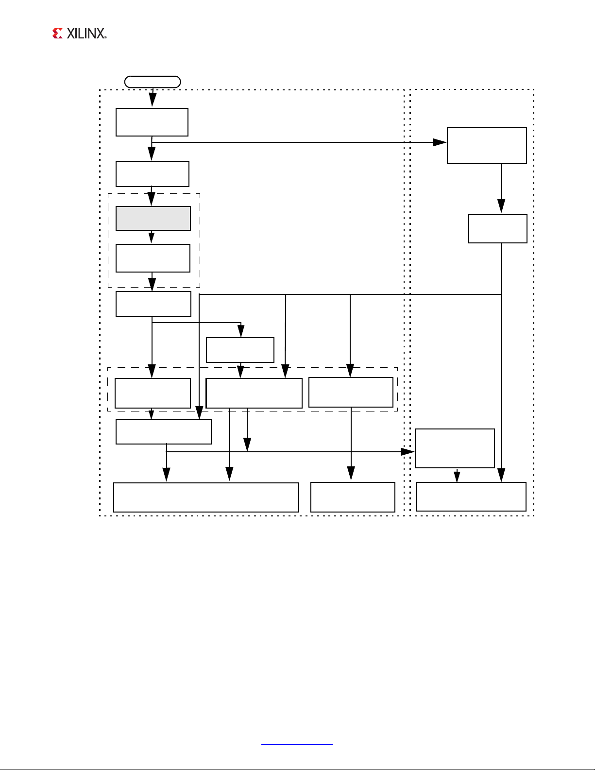
Tool Flow
The MicroBlaze MCS uses the generic tool flow of all Vivado IP. The SDK software
development flow is briefly described here.
Generic Vivado Tool Flow
The generic tool flow in Vivado is shown in Figure 4-8.
X-Ref Target - Figure 4-8
Figure 4-8: Generic Vivado Tool Flow
MicroBlaze Micro Controller System v1.3 www.xilinx.com 29
PG048 December 18, 2012
Page 31

Chapter 4: Customizing and Generating the Core
This flow shows the specific steps required to implement a project with the MicroBlaze MCS
in Vivado, and the relationship between the hardware and software tools.
• Associate ELF Files:
This is the only manual step in Vivado, performed by selecting Tools > Associate ELF
Files... in the menu. Initially, the default infinite loop ELF file, mb_bootloop_le.elf, is
associated with the MicroBlaze MCS core. ELF files for implementation and simulation
are specified separately.
Note:
by changes during software development in SDK, but need to be re-imported to apply any
changes.
The associated ELF files are imported into the project. This means that they are unaffected
The final bitstream updated with software is named download.bit, and is normally located
in the project directory project-name.runs/impl_1.
For additional information, see the Xilinx Vivado Manuals [Ref 9].
SDK
The SDK commands to achieve the MicroBlaze MCS specific steps above are detailed here:
• Import Hardware Description - For each MicroBlaze MCS component to import:
Select File > New > Project... in the menu.
°
Expand Xilinx, and select Hardware Platform Specification.
°
Click Next.
°
Click Browse, and navigate to the hardware description file:
°
- In PlanAhead™ this file is typically called project-name.srcs/sources_1/
ip/component-name/component-name_sdk.xml.
- In Project Navigator this file is typically called ipcore_dir/
component-name_sdk.xml.
Click Finish to perform the import.
°
After the hardware description has been imported, a standalone board support package
can be created, which provides MicroBlaze processor-specific code, and the I/O Module
software driver. The MicroBlaze MCS configuration is available in the generated file
microblaze_0/include/xparameters.h.
• Import Hardware Implementation:
Select Xilinx Tools > Program FPGA in the menu.
°
Click the first Browse button, and navigate to the bitstream:
°
MicroBlaze Micro Controller System v1.3 www.xilinx.com 30
PG048 December 18, 2012
Page 32

Chapter 4: Customizing and Generating the Core
-In Vivado or PlanAhead this file is typically called project-name.runs/
impl_1/toplevel.bit.
- In Project Navigator this file is typically called toplevel.bit.
Click the second Browse button, and navigate to the BMM file updated with block
°
RAM placement.
- In Vivado this file is typically called project-name.runs/impl_1/
toplevel_bd.bmm.
- In PlanAhead with one MicroBlaze MCS component, this file is typically called
project-name.srcs/sources_1/ip/component-name/
component_name_bd.bmm. With more than one MicroBlaze MCS component,
the merged BMM file updated with block RAM placement must be selected
instead.
- In Project Navigator with one MicroBlaze MCS component, this file is typically
called ipcore_dir/component_name_bd.bmm. With more than one
MicroBlaze MCS component, the merged BMM file updated with block RAM
placement must be selected instead.
Click Program to perform the import and program the FPGA.
°
For additional information, see the Xilinx SDK Help [Ref 6].
MicroBlaze Micro Controller System v1.3 www.xilinx.com 31
PG048 December 18, 2012
Page 33

Constraining the Core
Required Constraints
There are no required constraints for this core.
Device, Package, and Speed Grade Selections
There are no Device, Package or Speed Grade requirements for this core.
Chapter 5
Clock Frequencies
There are no specific clock frequency requirements for this core.
Clock Management
MicroBlaze MCS is fully synchronous with all clocked elements clocked by the Clk input.
Clock Placement
There are no specific Clock placement requirements for this core.
Banking
There are no specific Banking rules for this core.
MicroBlaze Micro Controller System v1.3 www.xilinx.com 32
PG048 December 18, 2012
Page 34

Chapter 5: Constraining the Core
Transceiver Placement
There are no Transceiver Placement requirements for this core.
I/O Standard and Placement
There are no specific I/O standards and placement requirements for this core.
MicroBlaze Micro Controller System v1.3 www.xilinx.com 33
PG048 December 18, 2012
Page 35

SECTION III: ISE DESIGN SUITE
Customizing and Generating the Core
Constraining the Core
MicroBlaze Micro Controller System v1.3 www.xilinx.com 34
PG048 December 18, 2012
Page 36

Chapter 6
Customizing and Generating the Core
This chapter includes information on using Xilinx tools to customize and generate the core
using the ISE® Design Suite.
GUI
The I/O Module parameters are divided in seven tabs: MCS, UART, FIT, PIT, GPO, GPI and
Interrupts. The MCS parameter tab is shown in Figure 6-1.
X-Ref Target - Figure 6-1
Figure 6-1: MCS Parameter Tab
• Instance Hierarchical Design Name - Defines the unique instance name of the core in
the design hierarchy. The path should indicate the full hierarchy from the top level. If
the core is directly instantiated at the top level, this is just the instance name.
MicroBlaze Micro Controller System v1.3 www.xilinx.com 35
PG048 December 18, 2012
Page 37

Chapter 6: Customizing and Generating the Core
• Input Clock Frequency (MHz) - This parameter should be set to the frequency of the
core input clock in MHz. The value is used to calculate the correct UART baud rate.
• Memory Size - Defines the local memory size, used to store the MicroBlaze processor
software program instructions and data. Increase this value if the software program
does not fit in available memory.
• Enable I/O Bus - Enables I/O Bus port.
• Enable Debug Support - When debug support is enabled, it is possible to debug
software via JTAG, from Xilinx Software Development Kit (SDK) or directly using the
Xilinx Microprocessor Debugger (XMD).
• Debug JTAG User-defined Register - Specifies the JTAG user-defined register for
debug. When more than one MicroBlaze MCS instance with debug enabled is included
in the same design, a unique JTAG register must be used for each instance. When a
single instance is used, the default value USER2 should be kept unchanged.
• Enable MicroBlaze Trace Bus - This option enables the MicroBlaze Trace bus, which
provides access to several internal processor signals for trace purposes.
The UART parameter tab is shown in Figure 6-2.
X-Ref Target - Figure 6-2
Figure 6-2: UART Parameter Tab
• Enable Receiver - Enables UART receiver for character input. This is automatically
connected to standard input (stdin) in the software program.
MicroBlaze Micro Controller System v1.3 www.xilinx.com 36
PG048 December 18, 2012
Page 38

Chapter 6: Customizing and Generating the Core
• Enable Transmitter - Enables UART transmitter for character output. This is
automatically connected to standard output (stdout) in the software program.
• Define Baud Rate - Sets the UART baud rate. To get the correct baud rate, the input
clock frequency must also be correctly defined.
• Programmable Baud Rate - Determines if the UART baud rate is programmable. The
default baud rate is calculated based on the input clock frequency and the defined
baud rate.
• Number of Data Bits - Defines the number of data bits used by the UART. Should
almost always be set to 8.
• Use Parity - Enable this parameter to use parity checking of the UART characters.
• Even or Odd Parity - Select odd or even parity. Only available when parity is used.
• Implement Receive Interrupt - Generate an interrupt when the UART has received a
character. When the interrupt is not enabled the UART must be polled to check if data
has been received.
• Implement Transmit Interrupt - Generate an interrupt when the UART has sent a
character. When the interrupt is not enabled the UART must be polled to wait until data
has been transmitted.
• Implement Error Interrupt - Generate an interrupt if an error occurs when the UART
receives a character. This error can be a framing error, an overrun error or a parity error
(if parity is used), When the interrupt is not enabled the UART must be polled to check
if an error has occurred after a character has been received.
MicroBlaze Micro Controller System v1.3 www.xilinx.com 37
PG048 December 18, 2012
Page 39

Chapter 6: Customizing and Generating the Core
The FIT parameter tab showing the parameters for one of the four timers is shown in
Figure 6-3.
X-Ref Target - Figure 6-3
Figure 6-3: FIT Parameter Tab
• Use FIT - Enable the Fixed Interval Timer.
• Number of Clocks Between Strobes - The number of clock cycles between each
strobe.
• Generate Interrupt - Generate an interrupt for each Fixed Interval Timer strobe.
MicroBlaze Micro Controller System v1.3 www.xilinx.com 38
PG048 December 18, 2012
Page 40

Chapter 6: Customizing and Generating the Core
The PIT parameter tab showing the parameters for one of the four timers is shown in
Figure 6-4.
X-Ref Target - Figure 6-4
Figure 6-4: PIT Parameter Tab
• Use PIT - Enable the Programmable Interval Timer.
• Number of Bits for Timer - The maximum number of cycles to count before stopping
or restarting.
• Shall Counter Value be Readable - The Programmable Interval Timer counter is
readable by software when this parameter is set.
RECOMMENDED: Unless resource usage is critical it is recommended that you keep this
enabled.
• Define Prescaler - Selects a prescaler as source for the Programmable Interval Timer
count. When no prescaler is selected the core input clock is used. Any Programmable
Interval Timer or Fixed Interval Timer can be used as prescaler, as well as a dedicated
external enable input.
• Generate Interrupt - Generate an interrupt when the Programmable Interval Timer has
counted down to zero.
MicroBlaze Micro Controller System v1.3 www.xilinx.com 39
PG048 December 18, 2012
Page 41

Chapter 6: Customizing and Generating the Core
The GPO parameter tab showing the parameters with one of the four General Purpose
Output ports enabled is shown in Figure 6-5.
X-Ref Target - Figure 6-5
Figure 6-5: GPO Parameter Tab
• Use GPO - Enable the General Purpose Output port.
• Number of Bits - Set the number of bits of the General Purpose Output port.
• Initial Value of GPO - Set the initial value of the General Purpose Output port. The
right most bit in the value is assigned to bit 0 of the port, the next right most to bit 1,
and so on.
MicroBlaze Micro Controller System v1.3 www.xilinx.com 40
PG048 December 18, 2012
Page 42

Chapter 6: Customizing and Generating the Core
The GPI parameter tab showing the parameters with one of the four General Purpose Input
ports enabled is shown in Figure 6-6.
X-Ref Target - Figure 6-6
Figure 6-6: GPI Parameter Tab
• Use GPI - Enable the General Purpose Input port.
• Number of Bits - Set the number of bits of the General Purpose Input port.
• Generate Interrupt - Generate an interrupt when a General Purpose Input changes.
MicroBlaze Micro Controller System v1.3 www.xilinx.com 41
PG048 December 18, 2012
Page 43

Chapter 6: Customizing and Generating the Core
The Interrupts parameter tab is shown in Figure 6-7.
X-Ref Target - Figure 6-7
Figure 6-7: Interrupts Parameter Tab
• Use External Interrupts - Enable the use of external interrupt inputs.
• Number of External Inputs - Select the number of used external interrupt inputs.
• Level or Edge of External Interrupts - Select whether the input is considered level
sensitive or edge triggered. Each bit in the value corresponds to the equivalent
interrupt input. When a bit is set to one, the interrupt is edge triggered, otherwise it is
level sensitive.
• Positive or Negative External Interrupts - Set whether to use high or low level for
level sensitive interrupts, and rising or falling edge for edge triggered interrupts. Each
bit in the value corresponds to the equivalent interrupt input When a bit is set to one,
high level or rising edge is used, otherwise low level or falling edge is used.
• Use Low-latency Interrupt Handling - Enable the use of low-latency interrupt
handling.
MicroBlaze Micro Controller System v1.3 www.xilinx.com 42
PG048 December 18, 2012
Page 44

Chapter 6: Customizing and Generating the Core
Parameter Values
To create a MicroBlaze™ MCS that is uniquely tailored for a specific system, certain features
can be parameterized. This makes it possible to configure a component that only uses the
resources required by the system, and operates with the best possible performance. The
features that can be parameterized in MicroBlaze MCS are shown in Tabl e 4-1 .
The internal modules of the MicroBlaze MCS have fixed configurations detailed in:
• Ta bl e 4 -2 - MicroBlaze
• Ta bl e 4 -3 - I/O Module
• Ta bl e 4 -4 and Ta ble 4 -5 - LMB v10
• Ta bl e 4 -6 and Ta ble 4 -7 - LMB BRAM IF Controller
• Ta bl e 4 -8 - MicroBlaze Debug Module
Parameter - Port Dependencies
The width of many of the MicroBlaze MCS signals depends on design parameters. The
dependencies between the design parameters and I/O signals are shown in Tab le 4 -9.
Tool Flow
The MicroBlaze MCS uses the generic tool flow of all LogiCORE™ IP. This flow requires some
manual steps in PlanAhead™ and Project Navigator primarily to support software
development. For a brief description of the SDK software flow see SDK in Chapter 4.
Generic PlanAhead and Project Navigator Tool Flow
The generic tool flow in PlanAhead and Project Navigator is shown in Figure 6-8.
MicroBlaze Micro Controller System v1.3 www.xilinx.com 43
PG048 December 18, 2012
Page 45
X-Ref Target - Figure 6-8
Add CORE
Generator IP
Create
Merged
BMM
Implement
Project
Import
Hardware
Description
Import
Hardware
Create
Software
Software Development Kit
PlanAhead
Project Navigator
Implementation
Download
and Run
START
Update Tool
to Use BMM
Synthesize
Project
Update
Too l to
Use
Software
Ge ne r at e
Bitstream
Update
Bitstream
with
Software
Gen er at e
Bitstream
Download
and Run Software
Script
or
Debug Software
Gen er at e
Simulation
Files
Simulate
Software
Executable program (
program
.elf)
HW description XML file (
instance
_sdk.xml)
Bitstream (
toplevel
.bit)
Script
Create
Chapter 6: Customizing and Generating the Core
Figure 6-8: Generic PlanAhead and Project Navigator Tool Flow
This flow shows the specific steps required to implement a project with the MicroBlaze MCS
in PlanAhead or Project Navigator, and the relationship between the hardware and software
tools.
Each of the steps are described in general here. Specific commands used in PlanAhead, ISE
Project Navigator and Xilinx Software Development Kit (SDK) are covered in the following
sections.
• Add CORE Generator™ IP: In this step the specific MicroBlaze MCS component
parameters are defined using the configuration dialog, and the component is
generated and synthesized. Several files are created during this step:
MicroBlaze Micro Controller System v1.3 www.xilinx.com 44
PG048 December 18, 2012
Page 46

Chapter 6: Customizing and Generating the Core
component-name_sdk.xml - Hardware description of the specific component,
°
imported into SDK.
component-name.bmm - The BMM file of the specific component, which defines
°
the configuration of the block RAMs used by the component. This file is necessary
to update the bitstream with the software to be executed by MicroBlaze.
microblaze_mcs_setup.tcl - A script that is available to automate certain
°
steps in the flow.
mb_bootloop_le.elf - An infinite loop, which is the default program used to
°
update the bitstream.
Note:
frequency must be decided in this step, and adhered to when the component is later
instantiated.
The full hierarchical name of the component in the design as well as the input clock
• Create Merged BMM: This step is optional, and is only required when the project
contains more than one MicroBlaze MCS core.
The step can be performed by executing the script microblaze_mcs_setup.tcl in
the tool Tcl Console. The script creates a merged BMM file, called
microblaze_mcs_merged.bmm, which includes all MicroBlaze MCS components in
the project.
To perform the step manually, find all the MicroBlaze MCS core BMM files in the project,
and merge them using a text editor. The contents of the files can be concatenated in any
order, except that the id number at the end of each ADDRESS_MAP line (100 in the input
files) must be changed to a unique number for each ADDRESS MAP line. It is suggested
that you use the numbers 100, 200, ...
• Update Tool to Use BMM: This step informs the tool about the BMM file to use, either
the component BMM file, component-name.bmm, or he merged file from the previous
step when the project contains more than one MicroBlaze MCS core.
The step is also performed by executing the script microblaze_mcs_setup.tcl in
the tool Tcl Console. Project properties are updated to use the appropriate BMM file, by
adding a command line option to the ngdbuild command.
To perform the step manually, see the specific commands for PlanAhead or ISE Project
Navigator below.
• Implement Project: This is the normal step to create the implemented netlist.
• Update Tool to Use Software: This step informs the tool about the software
executable files to use, one for each MicroBlaze MCS component in the project. After
this step, whenever the bitstream is generated, it is updated with the contents of the
software executable files.
The step can be performed by invoking the microblaze_mcs_data2mem Tcl
procedure, with one argument for each MicroBlaze MCS component in the project,
MicroBlaze Micro Controller System v1.3 www.xilinx.com 45
PG048 December 18, 2012
Page 47

Chapter 6: Customizing and Generating the Core
indicating the corresponding software executable ELF file. Project properties are
updated to use the appropriate files, by adding a command line option to the bitgen
command.
To perform the step manually, see the specific commands for PlanAhead or ISE Project
Navigator below.
Note:
enter the ELF file arguments can be determined by first invoking the Tcl procedure without
arguments.
With more than one MicroBlaze MCS component in the project, the order in which to
• Gen erat e Bits tre am: This is the normal step to generate the bitstream, which creates
two hardware implementation files that can be imported into SDK, for running or
debugging software:
toplevel.bit - The bitstream created by the tools.
°
component-name_bd.bmm or microblaze_mcs_merged_bd.bmm - The BMM
°
file updated with block RAM placement. This file is used when updating the
bitstream with the software created in SDK.
If this step is performed after the tool has been updated to use software, the bitstream
is updated with the contents of the software executable files. If not, the bitstream can be
updated with software after it has been generated.
• Update Bitstream with Software: This step is used to update the previously generated
bitstream with all software executable files. If the software has been changed, this is the
only step necessary to modify the bitstream. It is not necessary to regenerate the
bitstream in this case.
The step is also performed by invoking the microblaze_mcs_data2mem Tcl
procedure. The procedure invokes data2mem to update the bitstream.
To perform the step manually, see the specific commands for PlanAhead or ISE Project
Navigator below.
• Gen erat e Sim ula tion Fil es: This step is used to generate MEM files used when
simulating the project. These files contain the memory content of all block RAMs used
when simulating the project. When behavioral simulation is started, the files are
automatically read by the simulator when elaborating the design.
The step is also performed by invoking the microblaze_mcs_data2mem Tcl
procedure. The procedure invokes data2mem to create the files
component-name.lmb_bram_n.mem for each MicroBlaze MCS component.
To perform the step manually, see the specific commands for PlanAhead or ISE Project
Navigator below.
• Download and Run Software: When downloading the updated bitstream to the FPGA
with impact, the software immediately starts to run as soon as reset is deactivated.
MicroBlaze Micro Controller System v1.3 www.xilinx.com 46
PG048 December 18, 2012
Page 48

Chapter 6: Customizing and Generating the Core
• Import Hardware Description: This step is performed in SDK, using the hardware
description file component-name_sdk.xml created when the MicroBlaze MCS
component was generated. If there are more than one component in the project, a
hardware platform specification must be imported for each component.
• Import Hardware Implementation: This step is performed in SDK, using the
toplevel.bit bitstream and the component-name_bd.bmm or
microblaze_mcs_merged_bd.bmm BMM file.
• Download and Run or Debug Software: When the FPGA has been programmed,
software can be run or debugged as usual in SDK.
PlanAhead
The PlanAhead commands to achieve the MicroBlaze MCS specific steps above are detailed
here.
Using the script provided to perform the steps:
• Create Merged BMM and Update Tool to Use BMM:
In the Tcl Console type the following commands:
cd project-path
source project-name.srcs/sources_1/ip/component-name/microblaze_mcs_setup.tcl
• Update Tool to Use Software, Update Bitstream with Software and Generate
Simulation Files:
Type the following command in the Tcl Console, to perform this with one MicroBlaze
MCS component:
microblaze_mcs_data2mem /sdk-workspace-path/sdk-program/Debug/sdk-program.elf
For each additional MicroBlaze MCS component, add an additional executable ELF file
to the command line.
Performing the steps manually:
• Update Tool to Use BMM:
With one MicroBlaze MCS component, type the following command in the Tcl Console,
using the appropriate absolute directory path:
config_run [current_run] -program ngdbuild -option {More Options} -value \
{-bm /project-path/project-name.srcs/sources_1/ip/component-name/
component-name_bd.bmm}
With more than one MicroBlaze MCS component, the -bm option must indicate the
merged BMM file instead.
MicroBlaze Micro Controller System v1.3 www.xilinx.com 47
PG048 December 18, 2012
Page 49

Chapter 6: Customizing and Generating the Core
• Update Tool to Use Software:
With one MicroBlaze MCS component, type the following command in the Tcl Console,
using the appropriate absolute directory path:
config_run [current_run] -program bitgen -option {More Options} -value \
{-bd /sdk-workspace-path/sdk-program/Debug/sdk-program.elf tag component-name}
With more than one MicroBlaze MCS component, the -bd option must be repeated for
each component.
• Update Bitstream with Software:
To perform this step with one MicroBlaze MCS component, invoke data2mem with, for
example, the following command line options, using the appropriate directory paths to
the indicated files:
cd project-path
data2mem -p part \
-bm project-name.srcs/sources_1/ip/component-name/component-name_bd.bmm \
-bd /sdk-workspace-path/sdk-program/Debug/sdk-program.elf tag component-name \
-bt project-name.runs/impl_1/toplevel.bit \
-o b project-name.runs/impl_1/download.bit
Here part is the complete part name, consisting of device, package, and speed
concatenated.
With more than one MicroBlaze MCS component, the -bm option must indicate the
merged BMM file.updated with block RAM placement.
For each additional MicroBlaze MCS component, the -bd option has to be repeated,
followed by the appropriate executable ELF file, the keyword tag, and the component
name.
• Gen erat e Sim ula tion Fil es:
To perform this step manually with one MicroBlaze MCS component, invoke data2mem
with, for example, the following command line options, using the appropriate directory
paths for the indicated files:
cd project-path
data2mem -p part \
-bm project-name.srcs/sources_1/ip/component-name/component-name.bmm \
-bd /sdk-workspace-path/sdk-program/Debug/sdk-program.elf tag component-name \
-bx project-name.sim/sim_1 -u
Here part is the complete part name, consisting of device, package, and speed
concatenated.
For each additional MicroBlaze MCS component, the -bd option has to be repeated,
followed by the appropriate executable ELF file, the keyword tag, and the component
name.
MicroBlaze Micro Controller System v1.3 www.xilinx.com 48
PG048 December 18, 2012
Page 50

Chapter 6: Customizing and Generating the Core
If the output directory indicated by the -bx option does not exist, it has to be created
manually.
For additional information, see the Xilinx PlanAhead Manuals [Ref 8].
Project Navigator
The Project Navigator commands to achieve the MicroBlaze MCS specific steps above are
detailed here.
Using the provided script to perform the steps:
• Create Merged BMM and Update Tool to Use BMM:
If the Tcl Console is not visible, select View > Panels > Tcl Console in the menu.
°
In the Tcl Console type the following command:
°
source ipcore_dir/microblaze_mcs_setup.tcl
• Update Tool to Use Software, Update Bitstream with Software and Generate
Simulation Files:
Type the following command in the Tcl Console, to perform this with one MicroBlaze
MCS component:
microblaze_mcs_data2mem /sdk-workspace-path/sdk-program/Debug/sdk-program.elf
For each additional MicroBlaze MCS component, add an additional executable ELF file
to the command line.
Performing the steps manually:
• Update Tool to Use BMM:
With one MicroBlaze MCS component, type the following command in the Tcl Console:
project set {Other Ngdbuild Command Line Options} {-bm ipcore_dir/
component-name_bd.bmm}
With more than one MicroBlaze MCS component, the -bm option must indicate the
merged BMM file instead.
• Update Tool to Use Software:
With one MicroBlaze MCS component, type the following command in the Tcl Console,
using the appropriate absolute directory path:
project set {Other Bitgen Command Line Options} \
{-bd /sdk-workspace-path/sdk-program/Debug/sdk-program.elf tag component-name}
MicroBlaze Micro Controller System v1.3 www.xilinx.com 49
PG048 December 18, 2012
Page 51

Chapter 6: Customizing and Generating the Core
With more than one MicroBlaze MCS component, the -bd option must be repeated for
each component.
• Update Bitstream with Software:
To perform this step with one MicroBlaze MCS component, invoke data2mem with, for
example, the following command line options, using the appropriate directory paths to
the indicated files:
cd project-path
data2mem -p part \
-bm ipcore_dir/component-name_bd.bmm \
-bd /sdk-workspace-path/sdk-program/Debug/sdk-program.elf tag component-name \
-bt project-name.runs/impl_1/toplevel.bit \
-o b project-name.runs/impl_1/download.bit
Here part is the complete part name, consisting of device, package, and speed
concatenated.
With more than one MicroBlaze MCS component, the -bm option must indicate the
merged BMM file, updated with block RAM placement.
For each additional MicroBlaze MCS component, the -bd option has to be repeated,
followed by the appropriate executable ELF file, the keyword tag, and the component
name.
• Gen erat e Sim ula tion Fil es:
To perform this step manually with one MicroBlaze MCS component, invoke data2mem
with, for example, the following command line options, using the appropriate directory
paths for the indicated files:
cd project-path
data2mem -p part \
-bm ipcore_dir/component-name.bmm \
-bd /sdk-workspace-path/sdk-program/Debug/sdk-program.elf tag component-name \
-bx . -u
Here part is the complete part name, consisting of device, package, and speed
concatenated.
For each additional MicroBlaze MCS component, the -bd option has to be repeated,
followed by the appropriate executable ELF file, the keyword tag, and the component
name.
For additional information, see the Xilinx ISE Manuals [Ref 7].
MicroBlaze Micro Controller System v1.3 www.xilinx.com 50
PG048 December 18, 2012
Page 52

Constraining the Core
Clock Management
MicroBlaze MCS is fully synchronous with all clocked elements clocked by the Clk input.
Chapter 7
MicroBlaze Micro Controller System v1.3 www.xilinx.com 51
PG048 December 18, 2012
Page 53

SECTION IV: APPENDICES
Application Software Development
Debugging
Additional Resources
MicroBlaze Micro Controller System v1.3 www.xilinx.com 52
PG048 December 18, 2012
Page 54

Appendix A
Application Software Development
Xilinx Software Development Kit
MicroBlaze MCS can be used with the Xilinx Software Development Kit (SDK), in the same
way as any embedded system.
The specific steps needed with MicroBlaze MCS are described in SDK in Chapter 4.
Device Drivers
The I/O Module is supported by the I/O Module driver, included with Xilinx Software
Development Kit.
MicroBlaze Micro Controller System v1.3 www.xilinx.com 53
PG048 December 18, 2012
Page 55

Debugging
This appendix includes details about resources available on the Xilinx Support website and
debugging tools. In addition, this appendix provides a step-by-step debugging process to
guide you through debugging the MicroBlaze MCS core.
The following topics are included in this appendix:
• Finding Help on Xilinx.com
• Debug Tools
• Troubleshooting
• Simulation Debug
• Hardware Debug
Appendix B
Finding Help on Xilinx.com
To help in the design and debug process when using the MicroBlaze MCS, the Xilinx
Support web page (www.xilinx.com/support) contains key resources such as product
documentation, release notes, answer records, information about known issues, and links
for opening a Technical Support WebCase.
Documentation
This product guide is the main document associated with the MicroBlaze MCS. This guide,
along with documentation related to all products that aid in the design process, can be
found on the Xilinx Support web page (www.xilinx.com/support
Documentation Navigator.
Download the Xilinx Documentation Navigator from the Design Tools tab on the Downloads
page (www.xilinx.com/download
available, open the online help after installation.
). For more information about this tool and the features
) or by using the Xilinx
MicroBlaze Micro Controller System v1.3 www.xilinx.com 54
PG048 December 18, 2012
Page 56

Appendix B: Debugging
Release Notes
Known issues for all cores, including the MicroBlaze MCS are described in the IP Release
Notes Guide (XTP025).
Known Issues
Answer Records include information about commonly encountered problems, helpful
information on how to resolve these problems, and any known issues with a Xilinx product.
Answer Records are created and maintained daily ensuring that users have access to the
most accurate information available.
Answer Records for this core are listed below, and can also be located by using the Search
Support box on the main Xilinx support web page
proper keywords such as
•Product name
• Tool message(s)
. To maximize your search results, use
• Summary of the issue encountered
A filter search is available after results are returned to further target the results.
Answer Records for the MicroBlaze MCS
www.xilinx.com/support/answers/46420.htm
www.xilinx.com/support/answers/51538.htm
Contacting Technical Support
Xilinx provides premier technical support for customers encountering issues that require
additional assistance.
To contact Xilinx Technical Support:
1. Navigate to www.xilinx.com/support
2. Open a WebCase by selecting the WebCase
When opening a WebCase, include:
.
link located under Support Quick Links.
• Target FPGA including package and speed grade.
• All applicable Xilinx Design Tools and simulator software versions.
• Additional files based on the specific issue might also be required. See the relevant
sections in this debug guide for guidelines about which file(s) to include with the
WebCase.
MicroBlaze Micro Controller System v1.3 www.xilinx.com 55
PG048 December 18, 2012
Page 57

Appendix B: Debugging
Xilinx provides technical support at www.xilinx.com/support for this LogiCORE™ IP product
when used as described in the product documentation. Xilinx cannot guarantee timing,
functionality, or support of product if implemented in devices that are not defined in the
documentation, if customized beyond that allowed in the product documentation, or if
changes are made to any section of the design labeled DO NOT MODIFY.
Debug Tools
The main tool available to address MicroBlaze MCS design issues is the ChipScope™ Pro
tool.
ChipScope Pro Tool
The ChipScope Pro debugging tool inserts logic analyzer, bus analyzer, and virtual I/O cores
directly into your design. The ChipScope Pro debugging tool allows you to set trigger
conditions to capture application and integrated block port signals in hardware. Captured
signals can then be analyzed through the ChipScope Pro logic analyzer tool. For detailed
information for using the ChipScope Pro debugging tool, see www.xilinx.com/tools/
cspro.htm.
Reference Boards
All Xilinx development boards support MicroBlaze MCS. These boards can be used to
prototype designs and establish that the core can communicate with the system.
Troubleshooting
This section provides help in diagnosing and correcting issues that can occur with the
MicroBlaze™ MCS specific tool flow in the ISE® Design Suite. If an error not listed here is
encountered, see the corresponding tool documentation. For each listed error message, the
probable cause of the error, and the suggested corrective action is provided.
MicroBlaze Micro Controller System v1.3 www.xilinx.com 56
PG048 December 18, 2012
Page 58

Appendix B: Debugging
Step Create Merged BMM, Update Tool to Use BMM
Tcl Command: microblaze_mcs_setup
Error message: ERROR: Could not find a BMM file for instances. Please regenerate the MicroBlaze
MCS instances.
Possible causes: • With PlanAhead, the BMM file has not been generated after customizing a
MicroBlaze MCS instance, or after adding an existing IP.
• The BMM file has inadvertently been deleted.
Corrective actions: • With PlanAhead, select each instance and use Generate IP in the context menu,
or synthesize the project, and then invoke the command again.
• With Project Navigator, double-click on each MicroBlaze MCS instance to
regenerate it, and then invoke the command again.
Step: Implement Project
Tool: Ngdbuild
Error message: NgdBuild:989 - Failed to process BMM information
Possible causes: • The parameter “Instance Hierarchical Design Name” set in the MicroBlaze MCS
configuration dialog does not match the actual instantiation name or place in the
instantiation hierarchy. Note that this is case sensitive in the tools.
• The parameter “Memory Size” set in the MicroBlaze MCS configuration dialog has
changed, but the corresponding BMM file has not been updated.
Corrective action: • Change “Instance Hierarchical Design Name” to the correct value in the
MicroBlaze MCS configuration dialog. This is the actual name used in the
instantiation, prefixed with all hierarchical levels below the top instance,
separated with /.
• Regenerate the BMM file according to the previous item.
Step: Implement Project
Tool: Ngdbuild
Error message: NgdBuild:634 - Cannot open input BMM file
Possible causes: The Ngdbuild -bm option does not indicate the correct BMM file.
Corrective action: Change the Ngdbuild option, either manually, or by invoking
microblaze_mcs_setup in the Tcl Console.
Step: Implement Project
Tool: Ngdbuild
Error message: NgdBuild:76 - File "path/component-name.ngc" cannot be merged into block
"instance-name" (TYPE="component-name") because one or more pins on the block,
including pin "pin-name", were not found in the file. Please make sure that all pins
on the instantiated component match pins in the lower-level design block
(irrespective of case). If there are bussed pins on this block, make sure that the
upper-level and lower-level netlists use the same bus-naming convention.
MicroBlaze Micro Controller System v1.3 www.xilinx.com 57
PG048 December 18, 2012
Page 59

Appendix B: Debugging
Step: Implement Project
Possible causes: The instantiation does not match the MicroBlaze MCS component, with one or more
different input pins.
Corrective action: Change the instantiation to match the template in component-name.vho (VHDL
project) or component_name.veo (Verilog project).
Step: Update Tool to Use Software
Tcl Command: microblaze_mcs_data2mem
Error message: ERROR: Too many arguments. At most instance-count ELF files should be given.
Possible causes: • The command has not been invoked with the correct number of arguments. There
should be at most one argument per MicroBlaze MCS core.
• The paths to the ELF files include space characters.
Corrective action: • Invoke the command with the correct number of arguments. To check the number
of arguments, and their order, invoke the command without arguments. This
updates the project with the boot loop, and lists the detected cores in the order
the arguments should be given.
• Ensure that each path is enclosed in double quotes if it includes space characters.
Step: Update Bitstream with Software
Tcl Command: microblaze_mcs_data2mem
Error messages: • ERROR: Could not find BMM-filename. Please regenerate the MicroBlaze MCS
instance.
• ERROR: Could not find BMM-filename. Please invoke "microblaze_mcs_setup" and
implement the design.
Possible causes: • With PlanAhead, the BMM file has not been generated after customizing a
MicroBlaze MCS instance, or after adding an existing IP.
• The BMM file has inadvertently been deleted.
Corrective action: • With PlanAhead, select each instance and use Generate IP in the context menu,
or synthesize the project, invoke the microblaze_mcs_setup command again,
and then implement the design.
• With Project Navigator, double-click on each MicroBlaze MCS instance to
regenerate it, invoke the microblaze_mcs_setup command again, and then
implement the design.
Step: Update Bitstream with Software
Tcl Command: microblaze_mcs_data2mem
Error messages: • ERROR: Could not find ELF-filename. Please make sure the file exists.
•ERROR: filename is not an ELF file.
Possible causes: • The command has not been invoked with the correct file names or paths.
• The executable file extension must be .elf.
• The paths to the ELF files include space characters.
• The paths to the ELF files do not follow Tcl syntax.
Corrective action: • Invoke the command with the correct file names and paths.
• Ensure that the file extension is correct.
• Ensure that each path is enclosed in double quotes if it includes space characters.
• The path separator character must be /.
MicroBlaze Micro Controller System v1.3 www.xilinx.com 58
PG048 December 18, 2012
Page 60

Appendix B: Debugging
Step: Update Bitstream with Software
Tool: Data2MEM
Error messages: ERROR:Data2MEM:31 - Out of bounds code segment for ram space in
'BMM-filename'.
Memory space 'component-name.lmb_bram' occupies [address-range]
Code segment index occupies [address-range]
Possible causes: The MicroBlaze MCS core memory size is smaller than the size used when creating
the software application.
Corrective action: • Increase the memory size in the MicroBlaze MCS configuration dialog.
• Open SDK to automatically detect the changed hardware configuration, and build
the program for the available memory size. Should the program not fit in
available memory, an error will occur. In this case, increase the memory size in the
MicroBlaze MCS configuration dialog.
Step: Generate Bitstream
Too l: Bit ge n
Error message: The design 'toplevel.ncd' is missing any BMM information for given block RAM data
files. BRAMs cannot be initialized with the given data without BMM information.
Either BMM information must be given to NGDBuild with a '-bm' option, or
embedded BMM information must be included in the source HDL.
Possible causes: The design has been implemented without the Ngdbuild -bm option to define the
BMM file, but with the Bitgen -bd option to define the used ELF files.
Corrective action: Add the Ngdbuild option, either manually, or by invoking the microblaze_mcs_setup
command, and then implement the design again.
Step: Simulate Software
Too l: ISi m
Error message: ERROR:HDLCompiler:1030 - "path/vhdl/src/unisims/primitive/RAMB16BWER.vhd"
Line 681: Cannot open file 'int_inf ile'.
Possible causes: The MEM files have not been generated, or are not located in the correct place.
Corrective actions: • Run Data2MEM manually to create simulation files, or invoke the
microblaze_mcs_data2mem command with the appropriate ELF files as
arguments.
• Move the MEM files to the correct place. In PlanAhead, the files are placed in the
sim_1 simulation set directory by default. If another simulation set is used, they
must be moved to that directory.
Step: Simulate Software
Too l: Mod el Si m
Error message: ERROR:Simulator:777 - Static elaboration of top level VHDL design unit tb in library
work failed
** Fatal: (vsim-7) Failed to open VHDL file "component-name.lmb_bram_index.mem"
in r mode.
Possible causes: The MEM files have not been generated.
MicroBlaze Micro Controller System v1.3 www.xilinx.com 59
PG048 December 18, 2012
Page 61

Appendix B: Debugging
Step: Simulate Software
Corrective actions: Run Data2MEM manually to create simulation files, or invoke the
microblaze_mcs_data2mem command with the appropriate ELF files as
arguments.
Step: Download and Run Software
Too l: Imp ac t
Problem: No output or mangled output on the UART console.
Possible causes: • The bitstream has not been configured with software.
• Frequency defined in the MicroBlaze MCS settings does not match actual
frequency of the connected clock input.
• Baud rate and/or other UART setting, defined in the MicroBlaze MCS settings, do
not match the terminal program settings.
Corrective actions: • Run data2mem manually to configure the bitstream with software, or invoke the
microblaze_mcs_data2mem command with the appropriate ELF files as
arguments.
• Correct the frequency in the MicroBlaze MCS configuration dialog.
• Change the terminal program settings to match the MicroBlaze MCS
configuration.
Simulation Debug
The simulation debug flow for ModelSim is described below. A similar approach can be
used with other simulators.
• Check for the latest supported versions of ModelSim in the Xilinx Design Tools: Release
Notes Guide. Is this version being used? If not, update to this version.
• If using Verilog, do you have a mixed mode simulation license? If not, obtain a
mixed-mode license.
• Ensure that the proper libraries are compiled and mapped. In ISE Project Navigator this
is done by clicking on Simulation view, selecting the device in Behavioral Hierarchy
and then selecting Run in the context menu for Compile HDL Simulation Libraries in
the Design tab below. In PlanAhead and Vivado Design Suite Flow
Settings can be used to define the libraries.
• Have you associated the intended software program for the MicroBlaze processor with
the simulation? Use the microblaze_mcs_data2mem Tcl procedure to do this in ISE
Project Navigator or PlanAhead. The equivalent command in Vivado Design Suite is
Tools
> Associate ELF Files.
> Simulation
MicroBlaze Micro Controller System v1.3 www.xilinx.com 60
PG048 December 18, 2012
Page 62

Appendix B: Debugging
Hardware Debug
This section provides debug steps for common issues. The ChipScope debugging tool is a
valuable resource to use in hardware debug.
General Checks
Ensure that all the timing constraints for the core were properly incorporated from the
example design and that all constraints were met during implementation.
• Does it work in post-place and route timing simulation? If problems are seen in
hardware but not in timing simulation, this could indicate a PCB issue. Ensure that all
clock sources are active and clean.
• If using MMCMs in the design, ensure that all MMCMs have obtained lock by
monitoring the LOCKED port.
MicroBlaze Micro Controller System v1.3 www.xilinx.com 61
PG048 December 18, 2012
Page 63

Additional Resources
Xilinx Resources
For support resources such as Answers, Documentation, Downloads, and Forums, see the
Xilinx Support website at:
Appendix C
www.xilinx.com/support
For a glossary of technical terms used in Xilinx documentation, see:
www.xilinx.com/company/terms.htm
.
.
References
These documents provide supplemental material useful with this user guide:
1. Local Memory Bus (LMB) V10 Product Guide (PG087
2. IP Processor LMB BRAM Interface Controller Product Guide (PG061
3. MicroBlaze Debug Module (MDM) Product Guide (PG062
4. I/O Module Product Guide (PG052
5. MicroBlaze Processor Reference Guide (UG081
6. Xilinx SDK Help
7. Xilinx ISE Manuals
)
)
)
)
)
8. Xilinx PlanAhead Manuals
9. Xilinx Vivado Manuals
10. 7 Series FPGAs Configuration User Guide (UG470)
MicroBlaze Micro Controller System v1.3 www.xilinx.com 62
PG048 December 18, 2012
Page 64

Appendix C: Additional Resources
Revision History
The following table shows the revision history for this document.
Date Version Revision
07/25/12 1.0 Initial Xilinx release. This Product Guide is derived from ds865.
12/18/12 1.1 Updated due to new core version. Updated Appendix B, Debugging.
Notice of Disclaimer
The information disclosed to you hereunder (the “Materials”) is provided solely for the selection and use of Xilinx products. To the
maximum extent permitted by applicable law: (1) Materials are made available “AS IS” and with all faults, Xilinx hereby DISCLAIMS
ALL WARRANTIES AND CONDITIONS, EXPRESS, IMPLIED, OR STATUTORY, INCLUDING BUT NOT LIMITED TO WARRANTIES OF
MERCHANTABILITY, NON-INFRINGEMENT, OR FITNESS FOR ANY PARTICULAR PURPOSE; and (2) Xilinx shall not be liable (whether
in contract or tort, including negligence, or under any other theor y of liability) for any loss or damage of any kind or nature related
to, arising under, or in connection with, the Materials (including your use of the Materials), including for any direct, indirect,
special, incidental, or consequential loss or damage (including loss of data, profits, goodwill, or any type of loss or damage
suffered as a result of any action brought by a third party) even if such damage or loss was reasonably foreseeable or Xilinx had
been advised of the possibility of the same. Xilinx assumes no obligation to correct any errors contained in the Materials or to
notify you of updates to the Materials or to product specif ications. You may not reproduce, modify, distribute, or publicly display
the Materials without prior written consent. Certain products are subject to the terms and conditions of the Limited Warranties
which can be viewed at http://www.xilinx.com/warranty.htm
a license issued to you by Xilinx. Xilinx products are not designed or intended to be fail-safe or for use in any application requiring
fail-safe performance; you assume sole risk and liability for use of Xilinx products in Critical Applications: http://www.xilinx.com/
warranty.htm#critapps.
; IP cores may be subject to warranty and support terms contained in
Automotive Applications Disclaimer
XILINX PRODUCTS ARE NOT DESIGNED OR INTENDED TO BE FAIL-SAFE, OR FOR USE IN ANY APPLICATION REQUIRING FAIL-SAFE
PERFORMANCE, SUCH AS APPLICATIONS RELATED TO: (I) THE DEPLOYMENT OF AIRBAGS, (II) CONTROL OF A VEHICLE, UNLESS
THERE IS A FAIL-SAFE OR REDUNDANCY FEATURE (WHICH DOES NOT INCLUDE USE OF SOFTWARE IN THE XILINX DEVICE TO
IMPLEMENT THE REDUNDANCY) AND A WARNING SIGNAL UPON FAILURE TO THE OPERATOR, OR (III) USES THAT COULD LEAD
TO DEATH OR PERSONAL INJURY. CUSTOMER ASSUMES THE SOLE RISK AND LIABILITY OF ANY USE OF XILINX PRODUCTS IN
SUCH APPLICATIONS.
© Copyright 2012 Xilinx, Inc. Xilinx, the Xilinx logo, Artix, ISE, Kintex, Spartan, Virtex, Vivado, Zynq, and other designated brands
included herein are trademarks of Xilinx in the United States and other countries. All other trademarks are the property of their
respective owners.
MicroBlaze Micro Controller System v1.3 www.xilinx.com 63
PG048 December 18, 2012
 Loading...