

Page 1

MicroBlaze
Processor
Reference Guide
Embedded Development Kit
EDK 8.2i
UG081 (v6.0) June 1, 2006
R
Page 2

© 2006 Xilinx, Inc. All Rights Reserved. XILINX, the Xilinx logo, and other designated brandsincludedhereinaretrademarksofXilinx,Inc.
All other trademarks are the property of their respective owners.
NOTICEOFDISCLAIMER:Xilinxis providing this design, code, or information "as is." By providing the design, code, or information as one
possible implementation of this feature, application, or standard, Xilinx makes no representation that this implementation is free from any
claims of infringement. You are responsible for obtaining any rights you may require for your implementation. Xilinx expressly disclaims any
warranty whatsoever with respect to the adequacy of the implementation, including but not limited to any warranties or representations that
this implementation is free from claims of infringement and any implied warranties of merchantability or fitness for a particular purpose.
MicroBlaze Processor Reference Guide www.xilinx.com UG081 (v6.0) June 1, 2006
1-800-255-7778
Page 3

MicroBlaze Processor Reference Guide
UG081 (v6.0) June 1, 2006
The following table shows the revision history for this document.
Date Version Revision
10/01/02 1.0 Xilinx EDK 3.1 release
03/11/03 2.0 Xilinx EDK 3.2 release
09/24/03 3.0 Xilinx EDK 6.1 release
02/20/04 3.1 Xilinx EDK 6.2 release
08/24/04 4.0 Xilinx EDK 6.3 release
09/21/04 4.1 Minor corrections for EDK 6.3 SP1 release
11/18/04 4.2 Minor corrections for EDK 6.3 SP2 release
01/20/05 5.0 Xilinx EDK 7.1 release
04/02/05 5.1 Minor corrections for EDK 7.1 SP1 release
05/09/05 5.2 Minor corrections for EDK 7.1 SP2 release
10/05/05 5.3 Minor corrections for EDK 8.1 release
02/21/06 5.4 Corrections for EDK 8.1 SP2 release
06/01/06 6.0 Xilinx EDK 8.2 release
UG081 (v6.0) June 1, 2006 www.xilinx.com MicroBlaze Processor Reference Guide
1-800-255-7778
Page 4

MicroBlaze Processor Reference Guide www.xilinx.com UG081 (v6.0) June 1, 2006
1-800-255-7778
Page 5

Preface: About This Guide
Manual Contents. . . . . . . . . . . . . . . . . . . . . . . . . . . . . . . . . . . . . . . . . . . . . . . . . . . . . . . . . . . . . 7
Additional Resources . . . . . . . . . . . . . . . . . . . . . . . . . . . . . . . . . . . . . . . . . . . . . . . . . . . . . . . . 7
Conventions . . . . . . . . . . . . . . . . . . . . . . . . . . . . . . . . . . . . . . . . . . . . . . . . . . . . . . . . . . . . . . . . . 8
Typographical. . . . . . . . . . . . . . . . . . . . . . . . . . . . . . . . . . . . . . . . . . . . . . . . . . . . . . . . . . . . . 8
Online Document . . . . . . . . . . . . . . . . . . . . . . . . . . . . . . . . . . . . . . . . . . . . . . . . . . . . . . . . . . 9
Chapter 1: MicroBlaze Architecture
Overview . . . . . . . . . . . . . . . . . . . . . . . . . . . . . . . . . . . . . . . . . . . . . . . . . . . . . . . . . . . . . . . . . . . 11
Features . . . . . . . . . . . . . . . . . . . . . . . . . . . . . . . . . . . . . . . . . . . . . . . . . . . . . . . . . . . . . . . . . 11
Data Types and Endianness . . . . . . . . . . . . . . . . . . . . . . . . . . . . . . . . . . . . . . . . . . . . . . . . . 13
Instructions . . . . . . . . . . . . . . . . . . . . . . . . . . . . . . . . . . . . . . . . . . . . . . . . . . . . . . . . . . . . . . . . . 13
Registers. . . . . . . . . . . . . . . . . . . . . . . . . . . . . . . . . . . . . . . . . . . . . . . . . . . . . . . . . . . . . . . . . . . . 20
General Purpose Registers . . . . . . . . . . . . . . . . . . . . . . . . . . . . . . . . . . . . . . . . . . . . . . . . . 21
Special Purpose Registers . . . . . . . . . . . . . . . . . . . . . . . . . . . . . . . . . . . . . . . . . . . . . . . . . . 21
Pipeline Architecture. . . . . . . . . . . . . . . . . . . . . . . . . . . . . . . . . . . . . . . . . . . . . . . . . . . . . . . . 31
Branches. . . . . . . . . . . . . . . . . . . . . . . . . . . . . . . . . . . . . . . . . . . . . . . . . . . . . . . . . . . . . . . . . 32
Memory Architecture. . . . . . . . . . . . . . . . . . . . . . . . . . . . . . . . . . . . . . . . . . . . . . . . . . . . . . . . 32
Reset, Interrupts, Exceptions, and Break . . . . . . . . . . . . . . . . . . . . . . . . . . . . . . . . . . . . . 33
Reset . . . . . . . . . . . . . . . . . . . . . . . . . . . . . . . . . . . . . . . . . . . . . . . . . . . . . . . . . . . . . . . . . . . . 34
Hardware Exceptions . . . . . . . . . . . . . . . . . . . . . . . . . . . . . . . . . . . . . . . . . . . . . . . . . . . . . 34
Breaks. . . . . . . . . . . . . . . . . . . . . . . . . . . . . . . . . . . . . . . . . . . . . . . . . . . . . . . . . . . . . . . . . . . 35
Interrupt . . . . . . . . . . . . . . . . . . . . . . . . . . . . . . . . . . . . . . . . . . . . . . . . . . . . . . . . . . . . . . . . 36
User Vector (Exception) . . . . . . . . . . . . . . . . . . . . . . . . . . . . . . . . . . . . . . . . . . . . . . . . . . . 36
Instruction Cache . . . . . . . . . . . . . . . . . . . . . . . . . . . . . . . . . . . . . . . . . . . . . . . . . . . . . . . . . . . 37
Overview . . . . . . . . . . . . . . . . . . . . . . . . . . . . . . . . . . . . . . . . . . . . . . . . . . . . . . . . . . . . . . . . 37
General Instruction Cache Functionality . . . . . . . . . . . . . . . . . . . . . . . . . . . . . . . . . . . . . 37
Instruction Cache Operation . . . . . . . . . . . . . . . . . . . . . . . . . . . . . . . . . . . . . . . . . . . . . . . 38
Instruction Cache Software Support . . . . . . . . . . . . . . . . . . . . . . . . . . . . . . . . . . . . . . . . . 38
Data Cache. . . . . . . . . . . . . . . . . . . . . . . . . . . . . . . . . . . . . . . . . . . . . . . . . . . . . . . . . . . . . . . . . . 38
Overview . . . . . . . . . . . . . . . . . . . . . . . . . . . . . . . . . . . . . . . . . . . . . . . . . . . . . . . . . . . . . . . . 38
General Data Cache Functionality. . . . . . . . . . . . . . . . . . . . . . . . . . . . . . . . . . . . . . . . . . . 39
Data Cache Operation . . . . . . . . . . . . . . . . . . . . . . . . . . . . . . . . . . . . . . . . . . . . . . . . . . . . . 39
Data Cache Software Support . . . . . . . . . . . . . . . . . . . . . . . . . . . . . . . . . . . . . . . . . . . . . . 40
Floating Point Unit (FPU) . . . . . . . . . . . . . . . . . . . . . . . . . . . . . . . . . . . . . . . . . . . . . . . . . . . 40
Overview . . . . . . . . . . . . . . . . . . . . . . . . . . . . . . . . . . . . . . . . . . . . . . . . . . . . . . . . . . . . . . . . 40
Format . . . . . . . . . . . . . . . . . . . . . . . . . . . . . . . . . . . . . . . . . . . . . . . . . . . . . . . . . . . . . . . . . . 41
Rounding. . . . . . . . . . . . . . . . . . . . . . . . . . . . . . . . . . . . . . . . . . . . . . . . . . . . . . . . . . . . . . . . 41
Operations. . . . . . . . . . . . . . . . . . . . . . . . . . . . . . . . . . . . . . . . . . . . . . . . . . . . . . . . . . . . . . . 41
Exceptions . . . . . . . . . . . . . . . . . . . . . . . . . . . . . . . . . . . . . . . . . . . . . . . . . . . . . . . . . . . . . . . 42
Fast Simplex Link (FSL) . . . . . . . . . . . . . . . . . . . . . . . . . . . . . . . . . . . . . . . . . . . . . . . . . . . . . 42
Hardware Acceleration using FSL. . . . . . . . . . . . . . . . . . . . . . . . . . . . . . . . . . . . . . . . . . . 42
Debug and Trace. . . . . . . . . . . . . . . . . . . . . . . . . . . . . . . . . . . . . . . . . . . . . . . . . . . . . . . . . . . . 43
Debug Overview . . . . . . . . . . . . . . . . . . . . . . . . . . . . . . . . . . . . . . . . . . . . . . . . . . . . . . . . .43
Trace Overview . . . . . . . . . . . . . . . . . . . . . . . . . . . . . . . . . . . . . . . . . . . . . . . . . . . . . . . . . . 43
Chapter 2: MicroBlaze Signal Interface Description
Overview . . . . . . . . . . . . . . . . . . . . . . . . . . . . . . . . . . . . . . . . . . . . . . . . . . . . . . . . . . . . . . . . . . . 45
UG081 (v6.0) June 1, 2006 www.xilinx.com MicroBlaze Processor Reference Guide
1-800-255-7778
Page 6

Features . . . . . . . . . . . . . . . . . . . . . . . . . . . . . . . . . . . . . . . . . . . . . . . . . . . . . . . . . . . . . . . . . 45
MicroBlaze I/O Overview . . . . . . . . . . . . . . . . . . . . . . . . . . . . . . . . . . . . . . . . . . . . . . . . . . . 45
On-Chip Peripheral Bus (OPB) Interface Description . . . . . . . . . . . . . . . . . . . . . . . . 48
Local Memory Bus (LMB) Interface Description . . . . . . . . . . . . . . . . . . . . . . . . . . . . . 49
LMB Signal Interface . . . . . . . . . . . . . . . . . . . . . . . . . . . . . . . . . . . . . . . . . . . . . . . . . . . . . . 49
LMB Transactions . . . . . . . . . . . . . . . . . . . . . . . . . . . . . . . . . . . . . . . . . . . . . . . . . . . . . . . .51
Read and Write Data Steering . . . . . . . . . . . . . . . . . . . . . . . . . . . . . . . . . . . . . . . . . . . . . . 53
Fast Simplex Link (FSL) Interface Description . . . . . . . . . . . . . . . . . . . . . . . . . . . . . . . 54
Master FSL Signal Interface . . . . . . . . . . . . . . . . . . . . . . . . . . . . . . . . . . . . . . . . . . . . . . . . 54
Slave FSL Signal Interface. . . . . . . . . . . . . . . . . . . . . . . . . . . . . . . . . . . . . . . . . . . . . . . . . . 54
FSL Transactions . . . . . . . . . . . . . . . . . . . . . . . . . . . . . . . . . . . . . . . . . . . . . . . . . . . . . . . . . 55
Xilinx CacheLink (XCL) Interface Description . . . . . . . . . . . . . . . . . . . . . . . . . . . . . . . 55
CacheLink Signal Interface . . . . . . . . . . . . . . . . . . . . . . . . . . . . . . . . . . . . . . . . . . . . . . . . . 56
CacheLink Transactions . . . . . . . . . . . . . . . . . . . . . . . . . . . . . . . . . . . . . . . . . . . . . . . . . . . 57
Debug Interface Description . . . . . . . . . . . . . . . . . . . . . . . . . . . . . . . . . . . . . . . . . . . . . . . . 59
Trace Interface Description. . . . . . . . . . . . . . . . . . . . . . . . . . . . . . . . . . . . . . . . . . . . . . . . . . 59
MicroBlaze Core Configurability . . . . . . . . . . . . . . . . . . . . . . . . . . . . . . . . . . . . . . . . . . . . 61
Chapter 3: MicroBlaze Application Binary Interface
Scope . . . . . . . . . . . . . . . . . . . . . . . . . . . . . . . . . . . . . . . . . . . . . . . . . . . . . . . . . . . . . . . . . . . . . . . 65
Data Types. . . . . . . . . . . . . . . . . . . . . . . . . . . . . . . . . . . . . . . . . . . . . . . . . . . . . . . . . . . . . . . . . . 65
Register Usage Conventions. . . . . . . . . . . . . . . . . . . . . . . . . . . . . . . . . . . . . . . . . . . . . . . . . 66
Stack Convention . . . . . . . . . . . . . . . . . . . . . . . . . . . . . . . . . . . . . . . . . . . . . . . . . . . . . . . . . . . 67
Calling Convention . . . . . . . . . . . . . . . . . . . . . . . . . . . . . . . . . . . . . . . . . . . . . . . . . . . . . . .69
Memory Model . . . . . . . . . . . . . . . . . . . . . . . . . . . . . . . . . . . . . . . . . . . . . . . . . . . . . . . . . . . . . 69
Small data area . . . . . . . . . . . . . . . . . . . . . . . . . . . . . . . . . . . . . . . . . . . . . . . . . . . . . . . . . . . 69
Data area . . . . . . . . . . . . . . . . . . . . . . . . . . . . . . . . . . . . . . . . . . . . . . . . . . . . . . . . . . . . . . . . 69
Common un-initialized area. . . . . . . . . . . . . . . . . . . . . . . . . . . . . . . . . . . . . . . . . . . . . . . . 69
Literals or constants . . . . . . . . . . . . . . . . . . . . . . . . . . . . . . . . . . . . . . . . . . . . . . . . . . . . . . . 69
Interrupt and Exception Handling . . . . . . . . . . . . . . . . . . . . . . . . . . . . . . . . . . . . . . . . . . . 70
Chapter 4: MicroBlaze Instruction Set Architecture
Summary . . . . . . . . . . . . . . . . . . . . . . . . . . . . . . . . . . . . . . . . . . . . . . . . . . . . . . . . . . . . . . . . . . . 71
Notation . . . . . . . . . . . . . . . . . . . . . . . . . . . . . . . . . . . . . . . . . . . . . . . . . . . . . . . . . . . . . . . . . . . . 71
Formats . . . . . . . . . . . . . . . . . . . . . . . . . . . . . . . . . . . . . . . . . . . . . . . . . . . . . . . . . . . . . . . . . . . . . 72
Instructions . . . . . . . . . . . . . . . . . . . . . . . . . . . . . . . . . . . . . . . . . . . . . . . . . . . . . . . . . . . . . . . . . 72
UG081 (v6.0) June 1, 2006 www.xilinx.com MicroBlaze Processor Reference Guide
1-800-255-7778
Page 7
R
About This Guide
Welcome to the MicroBlaze Processor Reference Guide. This document provides
information about the 32-bit soft processor MicroBlaze, which is part of the Embedded
Processor Development Kit (EDK). The document is intended as a guide to the MicroBlaze
hardware architecture.
Manual Contents
This manual discusses the following topics specific to MicroBlaze soft processor:
• Core Architecture
• Bus Interfaces and Endianness
• Application Binary Interface
• Instruction Set Architecture
Preface
Additional Resources
For additional information, go to http://support.xilinx.com. The following table lists
some of the resources you can access from this web-site. You can also directly access these
resources using the provided URLs.
Resource Description/URL
Tutorials Tutorials covering Xilinx design flows, from design entry to
Answer Browser Database of Xilinx solution records
Application Notes Descriptions of device-specific design techniques and approaches
Data Book Pages from The Programmable Logic Data Book, which contains
verification and debugging
http://support.xilinx.com/support/techsup/tutorials/index.htm
http://support.xilinx.com/xlnx/xil_ans_browser.jsp
http://www.xilinx.com/xlnx/xweb/xil_publications_index.jsp?c
ategory=Application+Notes
device-specific information on Xilinx device characteristics,
including readback, boundary scan, configuration, length count,
and debugging
http://support.xilinx.com/xlnx/xweb/xil_publications_index.jsp
MicroBlaze Processor Reference Guide www.xilinx.com 7
UG081 (v6.0) June 1, 2006 1-800-255-7778
Page 8
R
Conventions
Typographical
Preface: About This Guide
Resource Description/URL
Problem Solvers Interactive tools that allow you to troubleshoot your design issues
http://support.xilinx.com/support/troubleshoot/psolvers.htm
Tech Tips Latest news, design tips, and patch information for the Xilinx
design environment
http://www.support.xilinx.com/xlnx/xil_tt_home.jsp
GNU Manuals The entire set of GNU manuals
http://www.gnu.org/manual
This document uses the following conventions. An example illustrates each convention.
The following typographical conventions are used in this document:
Convention Meaning or Use Example
Messages, prompts, and
Courier font
Courier bold
Helvetica bold
Italic font
Square brackets [ ]
program files that the system
displays
Literal commands that you
enter in a syntactical statement
Commands that you select
from a menu
Keyboard shortcuts Ctrl+C
Variables in a syntax
statement for which you must
supply values
References to other manuals
Emphasis in text
An optional entry or
parameter. However, in bus
specifications, such as
bus[7:0], they are required.
speed grade: - 100
ngdbuild design_name
File → Open
ngdbuild design_name
See the Development System
Reference Guide for more
information.
If a wire is drawn so that it
overlaps the pin of a symbol,
the two nets are not connected.
ngdbuild [option_name]
design_name
Braces { }
Vertical bar |
8 www.xilinx.com MicroBlaze Processor Reference Guide
A list of items from which you
must choose one or more
Separates items in a list of
choices
1-800-255-7778 UG081 (v6.0) June 1, 2006
lowpwr ={on|off}
lowpwr ={on|off}
Page 9
Conventions
R
Convention Meaning or Use Example
Vertical ellipsis
Horizontal ellipsis ...
Online Document
The following conventions are used in this document:
Convention Meaning or Use Example
Blue text
Red text
Blue, underlined text Hyperlink to a web-site (URL)
IOB #1: Name = QOUT’
.
.
Repetitive material that has
been omitted
.
Repetitive material that has
been omitted
Cross-reference link to a
location in the current file or
in another file in the current
document
Cross-reference link to a
location in another document
IOB #2: Name = CLKIN’
.
.
.
allow block block_name
loc1 loc2 ... locn;
See the section “Additional
Resources” for details.
Refer to “Title Formats” in
Chapter 1 for details.
See Figure 2-5 in the Virtex-II
Handbook.
Go to http://www.xilinx.com
for the latest speed files.
MicroBlaze Processor Reference Guide www.xilinx.com 9
UG081 (v6.0) June 1, 2006 1-800-255-7778
Page 10

R
Preface: About This Guide
10 www.xilinx.com MicroBlaze Processor Reference Guide
1-800-255-7778 UG081 (v6.0) June 1, 2006
Page 11
R
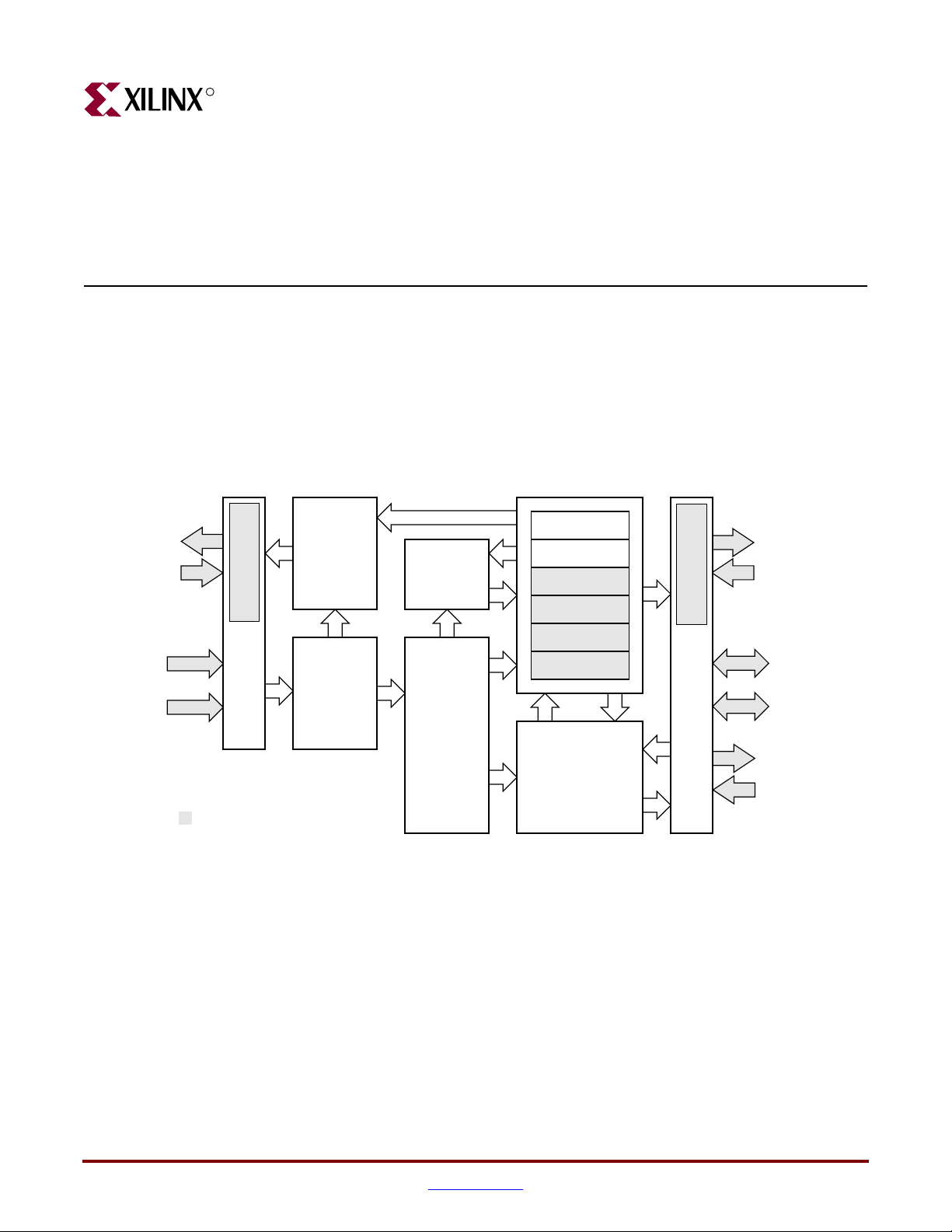
MicroBlaze Architecture
Overview
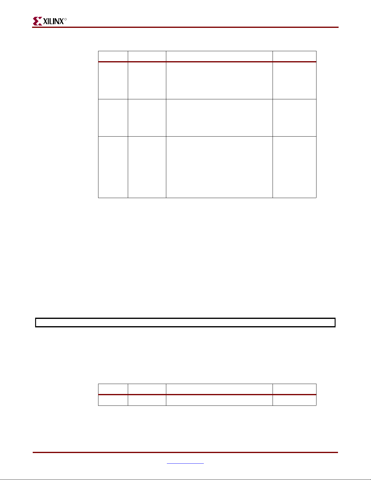
The MicroBlaze embedded processor soft core is a reduced instruction set computer (RISC)
optimized for implementation in Xilinx field programmable gate arrays (FPGAs).
Figure 1-1 shows a functional block diagram of the MicroBlaze core.
Chapter 1
IXCL_M
IXCL_S
Features
bus interface bus interface
I-Cache
IOPB
ILMB
Bus
IF
Optional MicroBlaze feature
Program
Counter
Instruction
Special
Purpose
Registers
Buffer
Instruction
Decode
ALU
Shift
Barrel Shift
Multiplier
Divider
FPU
Register File
32 X 32b
Figure 1-1: MicroBlaze Core Block Diagram
Data-sideInstruction-side
D-Cache
Bus
IF
DXCL_M
DXCL_S
DOPB
DLMB
MFSL 0..7
SFSL 0..7
The MicroBlaze soft core processor is highly configurable, allowing users to select a
specific set of features required by their design.
The processor’s fixed feature set includes:
• Thirty-two 32-bit general purpose registers
• 32-bit instruction word with three operands and two addressing modes
• 32-bit address bus
• Single issue pipeline
MicroBlaze Processor Reference Guide www.xilinx.com 11
UG081 (v6.0) June 1, 2006 1-800-255-7778
Page 12
R
Chapter 1: MicroBlaze Architecture
In addition to these fixed features the MicroBlaze processor is parametrized to allow
selective enabling of additional functionality. Older (deprecated) versions of MicroBlaze
support a subset of the optional features described in this manual. Only the latest (active)
version of MicroBlaze (v5.00a) supports all options.
Xilinx recommends that all new designs use the latest active version of the MicroBlaze
processor.
Table 1-1: Configurable Feature Overview by MicroBlaze Version
MicroBlaze Versions
Feature
v2.10a v3.00a v4.00a v5.00a
Version Status deprecated deprecated deprecated active
Processor pipeline depth 3 3 35
On-chip Peripheral Bus (OPB) data side interface option option option option
On-chip Peripheral Bus (OPB) instruction side interface option option option option
Local Memory Bus (LMB) data side interface option option option option
Local Memory Bus (LMB) instruction side interface option option option option
Hardware barrel shifter option option option option
Hardware divider option option option option
Hardware debug logic option option option option
Fast Simplex Link (FSL) interfaces 0-7 0-7 0-7 0-7
Machine status set and clear instructions option option option Yes
Instruction cache over IOPB interface option option option No
Data cache over IOPB interface option option option No
Instruction cache over CacheLink (IXCL) interface - option option option
Data cache over CacheLink (DXCL) interface - option option option
4 or 8-word cache line on XCL - 4 4 option
Hardware exception support - option option option
Pattern compare instructions - - option Yes
Floating point unit (FPU) - - option option
Disable hardware multiplier
1
- - option option
Hardware debug readable ESR and EAR - - Yes Yes
Processor Version Register (PVR) - - - option
1. Used in Virtex-II and subsequent families, for saving MUL18 and DSP48 primitives
12 www.xilinx.com MicroBlaze Processor Reference Guide
1-800-255-7778 UG081 (v6.0) June 1, 2006
Page 13
Data Types and Endianness
Data Types and Endianness
MicroBlaze uses Big-Endian, bit-reversed format to represent data. The hardware
supported data types for MicroBlaze are word, half word, and byte. The bit and byte
organization for each type is shown in the following tables.
Table 1-2: Word Data Type
R
Byte address n n+1 n+2 n+3
Byte label 0 1 2 3
Byte
significance
Bit label 0 31
Bit significance MSBit LSBit
Table 1-3: Half Word Data Type
Byte address n n+1
Byte label 0 1
Byte
significance
Bit label 0 15
Bit significance MSBit LSBit
Table 1-4: Byte Data Type
Byte address n
Bit label 0 7
MSByte LSByte
MSByte LSByte
Bit significance MSBit LSBit
Instructions
All MicroBlaze instructions are 32 bits and are defined as either Type A or TypeB. Type A
instructions have up to two source register operands and one destination register operand.
TypeB instructions have one sourceregister and a 16-bit immediate operand (which can be
extended to 32 bits by preceding the Type B instruction with an IMM instruction). Type B
instructions have a single destination register operand. Instructions are provided in the
following functional categories: arithmetic, logical, branch, load/store, and special.
Table 1-6 lists the MicroBlaze instruction set. Refer to Chapter 4, “MicroBlaze Instruction
Set Architecture”, for more information on these instructions. Table 1-5 describes the
instruction set nomenclature used in the semantics of each instruction.
MicroBlaze Processor Reference Guide www.xilinx.com 13
UG081 (v6.0) June 1, 2006 1-800-255-7778
Page 14

R
Chapter 1: MicroBlaze Architecture
Table 1-5: Instruction Set Nomenclature
Symbol Description
Ra R0 - R31, General Purpose Register, source operand a
Rb R0 - R31, General Purpose Register, source operand b
Rd R0 - R31, General Purpose Register, destination operand
SPR[x] Special Purpose Register number x
MSR Machine Status Register = SPR[1]
ESR Exception Status Register = SPR[5]
EAR Exception Address Register = SPR[3]
FSR Floating Point Unit Status Register = SPR[7]
PVRx Processor Version Register, where x is the register number = SPR[8192 + x]
BTR Branch Target Register = SPR[11]
PC Execute stage Program Counter = SPR[0]
x[y] Bit y of register x
x[y:z] Bit range y to z of register x
x Bit inverted value of register x
Imm 16 bit immediate value
Immxx bit immediate value
FSLx 3 bit Fast Simplex Link (FSL) port designator where x is the port number
C Carry flag, MSR[29]
Sa Special Purpose Register, source operand
Sd Special Purpose Register, destination operand
s(x) Sign extend argument x to 32-bit value
*Addr Memory contents at location Addr (data-size aligned)
:= Assignment operator
= Equality comparison
!= Inequality comparison
> Greater than comparison
>= Greater than or equal comparison
< Less than comparison
<= Less than or equal comparison
+ Arithmetic add
* Arithmetic multiply
/ Arithmetic divide
>> x Bit shift right x bits
14 www.xilinx.com MicroBlaze Processor Reference Guide
1-800-255-7778 UG081 (v6.0) June 1, 2006
Page 15
Instructions
Table 1-5: Instruction Set Nomenclature
Symbol Description
<< x Bit shift left x bits
and Logic AND
or Logic OR
xor Logic exclusive OR
op1 if cond else op2 Perform op1 if condition cond is true, else perform op2
& Concatenate. E.g. “0000100 & Imm7” is the concatenation of the fixed field “0000100” and
a 7 bit immediate value.
signed Operation performed on signed integer data type. All arithmetic operations are performed
on signed word operands, unless otherwise specified
unsigned Operation performed on unsigned integer data type
float Operation performed on floating point data type
R
Table 1-6: MicroBlaze Instruction Set Summary
Type A 0-5 6-10 11-15 16-20 21-31
Semantics
Type B 0-5 6-10 11-15 16-31
ADD Rd,Ra,Rb 000000 Rd Ra Rb 00000000000 Rd := Rb + Ra
RSUB Rd,Ra,Rb 000001 Rd Ra Rb 00000000000 Rd := Rb + Ra + 1
ADDC Rd,Ra,Rb 000010 Rd Ra Rb 00000000000 Rd := Rb + Ra + C
RSUBC Rd,Ra,Rb 000011 Rd Ra Rb 00000000000 Rd := Rb + Ra + C
ADDK Rd,Ra,Rb 000100 Rd Ra Rb 00000000000 Rd := Rb + Ra
RSUBK Rd,Ra,Rb 000101 Rd Ra Rb 00000000000 Rd := Rb + Ra + 1
ADDKC Rd,Ra,Rb 000110 Rd Ra Rb 00000000000 Rd := Rb + Ra + C
RSUBKC Rd,Ra,Rb 000111 Rd Ra Rb 00000000000 Rd := Rb + Ra + C
CMP Rd,Ra,Rb 000101 Rd Ra Rb 00000000001 Rd := Rb + Ra + 1
Rd[0] := 0 if (Rb >= Ra) else
Rd[0] := 1
CMPU Rd,Ra,Rb 000101 Rd Ra Rb 00000000011 Rd := Rb + Ra + 1 (unsigned)
Rd[0] := 0 if (Rb >= Ra, unsigned) else
Rd[0] := 1
ADDI Rd,Ra,Imm 001000 Rd Ra Imm Rd := s(Imm) + Ra
RSUBI Rd,Ra,Imm 001001 Rd Ra Imm Rd := s(Imm) + Ra + 1
ADDIC Rd,Ra,Imm 001010 Rd Ra Imm Rd := s(Imm) + Ra + C
RSUBIC Rd,Ra,Imm 001011 Rd Ra Imm Rd := s(Imm) + Ra + C
ADDIK Rd,Ra,Imm 001100 Rd Ra Imm Rd := s(Imm) + Ra
RSUBIK Rd,Ra,Imm 001101 Rd Ra Imm Rd := s(Imm) + Ra + 1
MicroBlaze Processor Reference Guide www.xilinx.com 15
UG081 (v6.0) June 1, 2006 1-800-255-7778
Page 16
R
Chapter 1: MicroBlaze Architecture
Table 1-6: MicroBlaze Instruction Set Summary (Continued)
Type A 0-5 6-10 11-15 16-20 21-31
Semantics
Type B 0-5 6-10 11-15 16-31
ADDIKC Rd,Ra,Imm 001110 Rd Ra Imm Rd := s(Imm) + Ra + C
RSUBIKC Rd,Ra,Imm 001111 Rd Ra Imm Rd := s(Imm) +
Ra + C
MUL Rd,Ra,Rb 010000 Rd Ra Rb 00000000000 Rd := Ra * Rb
BSRL Rd,Ra,Rb 010001 Rd Ra Rb 00000000000 Rd : = 0 & (Ra >> Rb)
BSRA Rd,Ra,Rb 010001 Rd Ra Rb 01000000000 Rd := s(Ra >> Rb)
BSLL Rd,Ra,Rb 010001 Rd Ra Rb 10000000000 Rd := (Ra << Rb) & 0
MULI Rd,Ra,Imm 011000 Rd Ra Imm Rd := Ra * s(Imm)
BSRLI Rd,Ra,Imm 011001 Rd Ra 00000000000 &
Rd : = 0 & (Ra >> Imm5)
Imm5
BSRAI Rd,Ra,Imm 011001 Rd Ra 00000010000 &
Rd := s(Ra >> Imm5)
Imm5
BSLLI Rd,Ra,Imm 011001 Rd Ra 00000100000 &
Rd := (Ra << Imm5) & 0
Imm5
IDIV Rd,Ra,Rb 010010 Rd Ra Rb 00000000000 Rd := Rb/Ra
IDIVU Rd,Ra,Rb 010010 Rd Ra Rb 00000000010 Rd := Rb/Ra, unsigned
FADD Rd,Ra,Rb 010110 Rd Ra Rb 00000000000 Rd := Rb+Ra, float
FRSUB Rd,Ra,Rb 010110 Rd Ra Rb 00010000000 Rd := Rb-Ra, float
FMUL Rd,Ra,Rb 010110 Rd Ra Rb 00100000000 Rd := Rb*Ra, float
FDIV Rd,Ra,Rb 010110 Rd Ra Rb 00110000000 Rd := Rb/Ra, float
1
1
1
1
FCMP.UN Rd,Ra,Rb 010110 Rd Ra Rb 01000000000 Rd := 1 if (Rb = NaN or Ra = NaN, float1)
else
Rd := 0
FCMP.LT Rd,Ra,Rb 010110 Rd Ra Rb 01000010000 Rd := 1 if (Rb < Ra, float1) else
Rd := 0
FCMP.EQ Rd,Ra,Rb 010110 Rd Ra Rb 01000100000 Rd := 1 if (Rb = Ra, float1) else
Rd := 0
FCMP.LE Rd,Ra,Rb 010110 Rd Ra Rb 01000110000 Rd := 1 if (Rb <= Ra, float1) else
Rd := 0
FCMP.GT Rd,Ra,Rb 010110 Rd Ra Rb 01001000000 Rd := 1 if (Rb > Ra, float1) else
Rd := 0
FCMP.NE Rd,Ra,Rb 010110 Rd Ra Rb 01001010000 Rd := 1 if (Rb != Ra, float1) else
Rd := 0
FCMP.GE Rd,Ra,Rb 010110 Rd Ra Rb 01001100000 Rd := 1 if (Rb >= Ra, float1) else
Rd := 0
GET Rd,FSLx 011011 Rd 00000 0000000000000 &
FSLx
Rd := FSLx (blocking data read)
MSR[FSL] := 1 if (FSLx_S_Control = 1)
16 www.xilinx.com MicroBlaze Processor Reference Guide
1-800-255-7778 UG081 (v6.0) June 1, 2006
Page 17

Instructions
Table 1-6: MicroBlaze Instruction Set Summary (Continued)
Type A 0-5 6-10 11-15 16-20 21-31
Type B 0-5 6-10 11-15 16-31
R
Semantics
PUT Ra,FSLx 011011 00000 Ra 1000000000000 &
FSLx := Ra (blocking data write)
FSLx
NGET Rd,FSLx 011011 Rd 00000 0100000000000 &
FSLx
Rd := FSLx (non-blocking data read)
MSR[FSL] := 1 if (FSLx_S_Control = 1)
MSR[C] := not FSLx_S_Exists
NPUT Ra,FSLx 011011 00000 Ra 1100000000000 &
FSLx
CGET Rd,FSLx 011011 Rd 00000 0010000000000 &
FSLx
CPUT Ra,FSLx 011011 00000 Ra 1010000000000 &
FSLx := Ra (non-blocking data write)
MSR[C] := FSLx_M_Full
Rd := FSLx (blocking control read)
MSR[FSL] := 1 if (FSLx_S_Control = 0)
FSLx := Ra (blocking control write)
FSLx
NCGET Rd,FSLx 011011 Rd 00000 0110000000000 &
FSLx
Rd := FSLx (non-blocking control read)
MSR[FSL] := 1 if (FSLx_S_Control = 0)
MSR[C] := not FSLx_S_Exists
NCPUT Ra,FSLx 011011 00000 Ra 1110000000000 &
FSLx
FSLx := Ra (non-blocking control write)
MSR[C] := FSLx_M_Full
OR Rd,Ra,Rb 100000 Rd Ra Rb 00000000000 Rd := Ra or Rb
AND Rd,Ra,Rb 100001 Rd Ra Rb 00000000000 Rd := Ra and Rb
XOR Rd,Ra,Rb 100010 Rd Ra Rb 00000000000 Rd := Ra xor Rb
ANDN Rd,Ra,Rb 100011 Rd Ra Rb 00000000000 Rd := Ra and
Rb
PCMPBF Rd,Ra,Rb 100000 Rd Ra Rb 10000000000 Rd := 1 if (Rb[0:7] = Ra[0:7]) else
Rd := 2 if (Rb[8:15] = Ra[8:15]) else
Rd := 3 if (Rb[16:23] = Ra[16:23]) else
Rd := 4 if (Rb[24:31] = Ra[24:31]) else
Rd := 0
PCMPEQ Rd,Ra,Rb 100010 Rd Ra Rb 10000000000 Rd := 1 if (Rd = Ra) else
Rd := 0
PCMPNE Rd,Ra,Rb 100011 Rd Ra Rb 10000000000 Rd := 1 if (Rd != Ra) else
Rd := 0
SRA Rd,Ra 100100 Rd Ra 0000000000000001 Rd := s(Ra >> 1)
C := Ra[31]
SRC Rd,Ra 100100 Rd Ra 0000000000100001 Rd := C & (Ra >> 1)
C := Ra[31]
SRL Rd,Ra 100100 Rd Ra 0000000001000001 Rd := 0 & (Ra >> 1)
C := Ra[31]
SEXT8 Rd,Ra 100100 Rd Ra 0000000001100000 Rd := s(Ra[24:31])
SEXT16 Rd,Ra 100100 Rd Ra 0000000001100001 Rd := s(Ra[16:31])
WIC Ra,Rb 100100 00000 Ra Rb 01101000 ICache_Tag := Ra
WDC Ra,Rb 100100 00000 Ra Rb 01100100 DCache_Tag := Ra
MicroBlaze Processor Reference Guide www.xilinx.com 17
UG081 (v6.0) June 1, 2006 1-800-255-7778
Page 18
R
Chapter 1: MicroBlaze Architecture
Table 1-6: MicroBlaze Instruction Set Summary (Continued)
Type A 0-5 6-10 11-15 16-20 21-31
Semantics
Type B 0-5 6-10 11-15 16-31
MTS Sd,Ra 100101 00000 Ra 11 & Sd SPR[Sd] := Ra, where:
• SPR[0x0001] is MSR
• SPR[0x0007] is FSR
MFS Rd,Sa 100101 Rd 00000 10 & Sa Rd := SPR[Sa], where:
• SPR[0x0000] is PC
• SPR[0x0001] is MSR
• SPR[0x0003] is EAR
• SPR[0x0005] is ESR
• SPR[0x0007] is FSR
• SPR[0x000B] is BTR
• SPR[0x2000:0x200B] is PVR[0] to
PVR[11]
MSRCLR Rd,Imm 100101 Rd 00001 00 & Imm14 Rd := MSR
MSR := MSR and
Imm14
MSRSET Rd,Imm 100101 Rd 00000 00 & Imm14 Rd := MSR
MSR := MSR or Imm14
BR Rb 100110 00000 00000 Rb 00000000000 PC := PC + Rb
BRD Rb 100110 00000 10000 Rb 00000000000 PC := PC + Rb
BRLD Rd,Rb 100110 Rd 10100 Rb 00000000000 PC := PC + Rb
Rd := PC
BRA Rb 100110 00000 01000 Rb 00000000000 PC := Rb
BRAD Rb 100110 00000 11000 Rb 00000000000 PC := Rb
BRALD Rd,Rb 100110 Rd 11100 Rb 00000000000 PC := Rb
Rd := PC
BRK Rd,Rb 100110 Rd 01100 Rb 00000000000 PC := Rb
Rd := PC
MSR[BIP] := 1
BEQ Ra,Rb 100111 00000 Ra Rb 00000000000 PC := PC + Rb if Ra = 0
BNE Ra,Rb 100111 00001 Ra Rb 00000000000 PC := PC + Rb if Ra != 0
BLT Ra,Rb 100111 00010 Ra Rb 00000000000 PC := PC + Rb if Ra < 0
BLE Ra,Rb 100111 00011 Ra Rb 00000000000 PC := PC + Rb if Ra <= 0
BGT Ra,Rb 100111 00100 Ra Rb 00000000000 PC := PC + Rb if Ra > 0
BGE Ra,Rb 100111 00101 Ra Rb 00000000000 PC := PC + Rb if Ra >= 0
BEQD Ra,Rb 100111 10000 Ra Rb 00000000000 PC := PC + Rb if Ra = 0
BNED Ra,Rb 100111 10001 Ra Rb 00000000000 PC := PC + Rb if Ra != 0
BLTD Ra,Rb 100111 10010 Ra Rb 00000000000 PC := PC + Rb if Ra < 0
BLED Ra,Rb 100111 10011 Ra Rb 00000000000 PC := PC + Rb if Ra <= 0
18 www.xilinx.com MicroBlaze Processor Reference Guide
1-800-255-7778 UG081 (v6.0) June 1, 2006
Page 19

Instructions
Table 1-6: MicroBlaze Instruction Set Summary (Continued)
Type A 0-5 6-10 11-15 16-20 21-31
Semantics
Type B 0-5 6-10 11-15 16-31
BGTD Ra,Rb 100111 10100 Ra Rb 00000000000 PC := PC + Rb if Ra > 0
BGED Ra,Rb 100111 10101 Ra Rb 00000000000 PC := PC + Rb if Ra >= 0
ORI Rd,Ra,Imm 101000 Rd Ra Imm Rd := Ra or s(Imm)
ANDI Rd,Ra,Imm 101001 Rd Ra Imm Rd := Ra and s(Imm)
XORI Rd,Ra,Imm 101010 Rd Ra Imm Rd := Ra xor s(Imm)
R
ANDNI Rd,Ra,Imm 101011 Rd Ra Imm Rd := Ra and
s(Imm)
IMM Imm 101100 00000 00000 Imm Imm[0:15] := Imm
RTSD Ra,Imm 101101 10000 Ra Imm PC := Ra + s(Imm)
RTID Ra,Imm 101101 10001 Ra Imm PC := Ra + s(Imm)
MSR[IE] := 1
RTBD Ra,Imm 101101 10010 Ra Imm PC := Ra + s(Imm)
MSR[BIP] := 0
RTED Ra,Imm 101101 10100 Ra Imm PC := Ra + s(Imm)
MSR[EE] := 1
MSR[EIP] := 0
ESR := 0
BRI Imm 101110 00000 00000 Imm PC := PC + s(Imm)
BRID Imm 101110 00000 10000 Imm PC := PC + s(Imm)
BRLID Rd,Imm 101110 Rd 10100 Imm PC := PC + s(Imm)
Rd := PC
BRAI Imm 101110 00000 01000 Imm PC := s(Imm)
BRAID Imm 101110 00000 11000 Imm PC := s(Imm)
BRALID Rd,Imm 101110 Rd 11100 Imm PC := s(Imm)
Rd := PC
BRKI Rd,Imm 101110 Rd 01100 Imm PC := s(Imm)
Rd := PC
MSR[BIP] := 1
BEQI Ra,Imm 101111 00000 Ra Imm PC := PC + s(Imm) if Ra = 0
BNEI Ra,Imm 101111 00001 Ra Imm PC := PC + s(Imm) if Ra != 0
BLTI Ra,Imm 101111 00010 Ra Imm PC := PC + s(Imm) if Ra < 0
BLEI Ra,Imm 101111 00011 Ra Imm PC := PC + s(Imm) if Ra <= 0
BGTI Ra,Imm 101111 00100 Ra Imm PC := PC + s(Imm) if Ra > 0
BGEI Ra,Imm 101111 00101 Ra Imm PC := PC + s(Imm) if Ra >= 0
BEQID Ra,Imm 101111 10000 Ra Imm PC := PC + s(Imm) if Ra = 0
BNEID Ra,Imm 101111 10001 Ra Imm PC := PC + s(Imm) if Ra != 0
BLTID Ra,Imm 101111 10010 Ra Imm PC := PC + s(Imm) if Ra < 0
MicroBlaze Processor Reference Guide www.xilinx.com 19
UG081 (v6.0) June 1, 2006 1-800-255-7778
Page 20
R
Chapter 1: MicroBlaze Architecture
Table 1-6: MicroBlaze Instruction Set Summary (Continued)
Type A 0-5 6-10 11-15 16-20 21-31
Semantics
Type B 0-5 6-10 11-15 16-31
BLEID Ra,Imm 101111 10011 Ra Imm PC := PC + s(Imm) if Ra <= 0
BGTID Ra,Imm 101111 10100 Ra Imm PC := PC + s(Imm) if Ra > 0
BGEID Ra,Imm 101111 10101 Ra Imm PC := PC + s(Imm) if Ra >= 0
LBU Rd,Ra,Rb 110000 Rd Ra Rb 00000000000 Addr := Ra + Rb
Rd[0:23] := 0
Rd[24:31] := *Addr[0:7]
LHU Rd,Ra,Rb 110001 Rd Ra Rb 00000000000 Addr := Ra + Rb
Rd[0:15] := 0
Rd[16:31] := *Addr[0:15]
LW Rd,Ra,Rb 110010 Rd Ra Rb 00000000000 Addr := Ra + Rb
Rd := *Addr
SB Rd,Ra,Rb 110100 Rd Ra Rb 00000000000 Addr := Ra + Rb
*Addr[0:8] := Rd[24:31]
SH Rd,Ra,Rb 110101 Rd Ra Rb 00000000000 Addr := Ra + Rb
*Addr[0:16] := Rd[16:31]
SW Rd,Ra,Rb 110110 Rd Ra Rb 00000000000 Addr := Ra + Rb
*Addr := Rd
LBUI Rd,Ra,Imm 111000 Rd Ra Imm Addr := Ra + s(Imm)
Rd[0:23] := 0
Rd[24:31] := *Addr[0:7]
LHUI Rd,Ra,Imm 111001 Rd Ra Imm Addr := Ra + s(Imm)
Rd[0:15] := 0
Rd[16:31] := *Addr[0:15]
LWI Rd,Ra,Imm 111010 Rd Ra Imm Addr := Ra + s(Imm)
Rd := *Addr
SBI Rd,Ra,Imm 111100 Rd Ra Imm Addr := Ra + s(Imm)
*Addr[0:7] := Rd[24:31]
SHI Rd,Ra,Imm 111101 Rd Ra Imm Addr := Ra + s(Imm)
*Addr[0:15] := Rd[16:31]
SWI Rd,Ra,Imm 111110 Rd Ra Imm Addr := Ra + s(Imm)
*Addr := Rd
1. Due to the many differentcorner cases involved in floating point arithmetic, only the normal behavior is described. A full description
of the behavior can be found in: Chapter 4, “MicroBlaze Instruction Set Architecture,”
Registers
MicroBlaze has an orthogonal instruction set architecture. It has thirty-two 32-bit general
purpose registers and up to seven 32-bit special purpose registers, depending on
configured options.
20 www.xilinx.com MicroBlaze Processor Reference Guide
1-800-255-7778 UG081 (v6.0) June 1, 2006
Page 21
Registers
General Purpose Registers
The thirty-two 32-bit General Purpose Registers are numbered R0 through R31. The
register file is reset on bit stream download (reset value is 0x00000000).
Note: The register file is not reset by the external reset inputs: reset and debug_rst.
0 31
↑
R0-R31
Figure 1-2: R0-R31
Table 1-7: General Purpose Registers (R0-R31)
Bits Name Description Reset Value
R
0:31 R0 R0 is defined to always have thevalue
0x00000000
of zero. Anything written to R0 is
discarded.
0:31 R1 through R13 R1 through R13 are 32-bit general
-
purpose registers
0:31 R14 32-bit used to store return addresses
-
for interrupts
0:31 R15 32-bit general purpose register 0:31 R16 32-bit used to store return addresses
-
for breaks
0:31 R17
0:31 R18 through R31 R18 through R31 are 32-bit general
If MicroBlaze is configured to support
hardware exceptions, this register is
loaded with HW exception return
address (see also “Branch Target
Register (BTR)”); if not it is a general
purpose register
-
-
purpose registers.
Please refer to Table 3-2 for software conventions on general purpose register usage.
Special Purpose Registers
Program Counter (PC)
The Program Counter is the 32-bit address of the execution instruction. It can be read with
an MFS instruction, but it can not be written to using an MTS instruction. When used with
the MFS instruction the PC register is specified by setting Sa = 0x0000.
MicroBlaze Processor Reference Guide www.xilinx.com 21
UG081 (v6.0) June 1, 2006 1-800-255-7778
Page 22
R
0 31
Chapter 1: MicroBlaze Architecture
↑
PC
Figure 1-3: PC
Table 1-8: Program Counter (PC)
Bits Name Description Reset Value
0:31 PC
Program Counter
0x00000000
Address of executing instruction,
i.e. “mfs r2 0” will store the address
of the mfs instruction itself in R2
Machine Status Register (MSR)
The Machine Status Register contains control and status bits for the processor. It can be
read with an MFS instruction. When reading the MSR, bit 29 is replicated in bit 0 as the
carry copy. MSR can be written using either an MTS instruction or the dedicated MSRSET
and MSRCLR instructions.
When writing to the MSR, some of the bits will takes effect immediately (e.g Carry) and the
remaining bits take effect one clock cycle later. Any value written to bit 0 is discarded.
When used with an MTS or MFS instruction the MSR is specified by setting Sx = 0x0001.
0 21 22 23 24 25 26 27 28 29 30 31
↑ ↑ ↑↑↑↑ ↑↑↑↑↑↑↑
CC RESERVED PVR EIP EE DCE DZ ICE FSL BIP C IE BE
Figure 1-4: MSR
Table 1-9: Machine Status Register (MSR)
Bits Name Description Reset Value
0CC
Arithmetic Carry Copy
0
Copy of the Arithmetic Carry (bit 29).
CC is always the same as bit C.
1:20 Reserved
21 PVR
22 www.xilinx.com MicroBlaze Processor Reference Guide
Processor Version Register exists
0 No Processor Version Register
1 Processor Version Register exists
Read only
1-800-255-7778 UG081 (v6.0) June 1, 2006
Based on
option
C_PVR
Page 23

Registers
R
Table 1-9: Machine Status Register (MSR) (Continued)
Bits Name Description Reset Value
22 EIP
23 EE
24 DCE
25 DZ
26 ICE
Exception In Progress
0 No hardware exception in progress
1 Hardware exception in progress
Read/Write
Exception Enable
0 Hardware exceptions disabled
1 Hardware exceptions enabled
Read/Write
Data Cache Enable
0 Data Cache is Disabled
1 Data Cache is Enabled
Read/Write
Division by Zero
1
0 No division by zero has occurred
1 Division by zero has occurred
Read/Write
Instruction Cache Enable
0 Instruction Cache is Disabled
1 Instruction Cache is Enabled
Read/Write
0
0
0
0
0
27 FSL
28 BIP
FSL Error
0 FSL get/put had no error
1 FSL get/put had mismatch in
control type
Read/Write
Break in Progress
0 No Break in Progress
1 Break in Progress
Source of break can be software break
instruction or hardware break from
Ext_Brk or Ext_NM_Brk pin.
Read/Write
0
0
MicroBlaze Processor Reference Guide www.xilinx.com 23
UG081 (v6.0) June 1, 2006 1-800-255-7778
Page 24
R
Chapter 1: MicroBlaze Architecture
Table 1-9: Machine Status Register (MSR) (Continued)
Bits Name Description Reset Value
29 C
Arithmetic Carry
0
0 No Carry (Borrow)
1 Carry (No Borrow)
Read/Write
30 IE
Interrupt Enable
0
0 Interrupts disabled
1 Interrupts enabled
Read/Write
31 BE
Buslock Enable
2
0
0 Buslock disabled on data-side OPB
1 Buslock enabled on data-side OPB
Buslock Enable does not affect
operation of IXCL, DXCL, ILMB,
DLMB, or IOPB.
Read/Write
1. This bit is only used for integer divide-by-zero signaling. There is a floating point equivalent
in the FSR. The DZ-bit will flag divide by zero conditions regardless if the processor is
configured with exception handling or not.
2. For a details on the OPB protocol, please refer to the IBM CoreConnect specification: 64-Bit
On-Chip Peripheral Bus, Architectural Specifications, Version 2.0.
Exception Address Register (EAR)
The Exception Address Register stores the full load/store address that caused the
exception. For an unaligned access exception that means the unaligned access address,and
for an DOPB exception, the failing OPB data access address. The contents of this register is
undefined for all other exceptions. When read with the MFS instruction the EAR is
specified by setting Sa = 0x0003.
0 31
↑
EAR
Figure 1-5: EAR
Table 1-10: Exception Address Register (EAR)
Bits Name Description Reset Value
0:31 EAR Exception Address Register 0x00000000
24 www.xilinx.com MicroBlaze Processor Reference Guide
1-800-255-7778 UG081 (v6.0) June 1, 2006
Page 25
Registers
Exception Status Register (ESR)
The Exception Status Register contains status bits for the processor. When read with the
MFS instruction the ESR is specified by setting Sa = 0x0005.
19 20 26 27 31
↑↑↑↑
RESERVED
Figure 1-6: ESR
Table 1-11: Exception Status Register (ESR)
Bits Name Description Reset Value
0:18 Reserved
DS
ESS EC
R
19 DS
20:26 ESS
27:31 EC
Exception in delay slot.
0 not caused by delay slot instruction
1 caused by delay slot instruction
Read-only
Exception Specific Status
For details refer to Table 1-12.
Read-only
Exception Cause
00001 = Unaligned data access exception
00010 = Illegal op-code exception
00011 = Instruction bus error exception
00100 = Data bus error exception
00101 = Divide by zero exception
00110 = Floating point unit exception
Read-only
0
See Table 1-12
0
MicroBlaze Processor Reference Guide www.xilinx.com 25
UG081 (v6.0) June 1, 2006 1-800-255-7778
Page 26
R
Chapter 1: MicroBlaze Architecture
Table 1-12: Exception Specific Status (ESS)
Exception
Cause
Bits Name Description Reset Value
Unaligned
Data Access
Illegal
Instruction
Instruction
bus error
Data bus
error
Divide by
zero
Floating
point unit
20 W
Word Access Exception
0 unaligned halfword access
1 unaligned word access
21 S Store Access Exception
0 unaligned load access
1 unaligned store access
22:26 Rx
Source/Destination Register
General purpose register used
as source (Store) or destination
(Load) in unaligned access
20:26 Reserved 0
20:26 Reserved 0
20:26 Reserved 0
20:26 Reserved 0
20:26 Reserved 0
0
0
0
Branch Target Register (BTR)
The Branch Target Register only exists if the MicroBlaze processor is configured to use
exceptions. The register stores the branch target address for all delay slot branch
instructions executed while MSR[EIP] = 0. If an exception is caused by an instruction in a
delay slot (i.e. ESR[DS]=1) then the exception handler should return execution to the
address stored in BTR instead of the normal exception return address stored in r17. When
read with the MFS instruction the BTR is specified by setting Sa = 0x000B.
0 31
↑
BTR
Figure 1-7: BTR
26 www.xilinx.com MicroBlaze Processor Reference Guide
1-800-255-7778 UG081 (v6.0) June 1, 2006
Page 27
Registers
R
Table 1-13: Branch Target Register (BTR)
Bits Name Description Reset Value
0:31 BTR Branch target address used by handler
0x00000000
when returning from an exception
caused by an instruction in a delay slot
Read-only
Floating Point Status Register (FSR)
The Floating Point Status Register contains status bits for the floating point unit. It can be
read with an MFS, and written with an MTS instruction. When read or written, the register
is specified by setting Sa = 0x0007.
27 28 29 30 31
↑ ↑↑↑↑↑
RESERVED IO DZ OF UF DO
Figure 1-8: FSR
Table 1-14: Floating Point Status Register (FSR)
Bits Name Description Reset Value
0:26 Reserved undefined
27 IO
28 DZ
29 OF
30 UF
31 DO
Invalid operation
Divide-by-zero
Overflow
Underflow
Denormalized operand error
0
0
0
0
0
Processor Version Register (PVR)
The Processor Version Register is controlled by the C_PVR configuration option on
MicroBlaze. When C_PVR is set to 0 the processor does not implement any PVR and
MSR[PVR]=0. If C_PVR is set to 1 then MicroBlaze implements only the first register:
PVR0, and if set to 2 all 12 PVR registers (PVR0 to PVR11) are implemented.
When read with the MFS instruction the PVR is specified by setting Sa = 0x200x, with x
being the register number between 0x0 and 0xB.
MicroBlaze Processor Reference Guide www.xilinx.com 27
UG081 (v6.0) June 1, 2006 1-800-255-7778
Page 28
R
Chapter 1: MicroBlaze Architecture
Table 1-15: Processor Version Register 0 (PVR0)
Bits Name Description Value
0 CFG PVR implementation: 0=basic,
Based on C_PVR
1=full
1 BS Use barrel shifter C_USE_BARREL
2 DIV Use divider C_USE_DIV
3 MUL Use hardware multiplier C_USE_HW_MUL
4 FPU Use FPU C_USE_FPU
5 EXC Use any type of exceptions Based on C_*_EXCEPTION
6 ICU Use instruction cache C_USE_ICACHE
7 DCU Use data cache C_USE_DCACHE
8:15 Reserved 0
16:23 MBV MicroBlaze release version code
Release Specific
0x1 = v5.00.a
24:31 USR1 User configured value 1 C_PVR_USER1
Table 1-16: Processor Version Register 1 (PVR1)
Bits Name Description Value
0:31 USR2 User configured value 2 C_PVR_USER2
Table 1-17: Processor Version Register 2 (PVR2)
Bits Name Description Value
0 DOPB Data side OPB in use C_D_OPB
1 DLMB Data side LMB in use C_D_LMB
2 IOPB Instruction side OPB in use C_I_OPB
3 IOPB Instruction side OPB in use C_I_LMB
4 IRQEDGE Interrupt is edge triggered C_INTERRUPT_IS_EDGE
5 IRQPOS Interrupt edge is positive C_EDGE_IS_POSITIVE
6:16 Reserved
17 BS Use barrel shifter C_USE_BARREL
18 DIV Use divider C_USE_DIV
19 MUL Use hardware multiplier C_USE_HW_MUL
20 FPU Use FPU C_USE_FPU
21:24 Reserved
28 www.xilinx.com MicroBlaze Processor Reference Guide
1-800-255-7778 UG081 (v6.0) June 1, 2006
Page 29
Registers
Table 1-17: Processor Version Register 2 (PVR2) (Continued)
Bits Name Description Value
R
25 OP0EXEC Generate exception for 0x0
illegal opcode
26 UNEXEC Generate exception for
unaligned data access
27 OPEXEC Generate exception for any
illegal opcode
28 IOPBEXEC Generate exception for IOPB
error
29 DOPBEXEC Generate exception for DOPB
error
30 DIVEXEC Generate exception for division
by zero
31 FPUEXEC Generate exceptions from FPU C_FPU_EXCEPTION
Table 1-18: Processor Version Register 3 (PVR3)
Bits Name Description Value
0 DEBUG Use debug logic C_DEBUG_ENABLED
1:2 Reserved
C_OPCODE_0x0_ILLEGAL
C_UNALIGNED_EXCEPTION
C_ILL_OPCODE_EXCEPTION
C_IOPB_BUS_EXCEPTION
C_DOPB_BUS_EXCEPTION
C_DIV_ZERO_EXCEPTION
3:6 PCBRK Number of PC breakpoints C_NUMBER_OF_PC_BRK
7:9 Reserved
10:12 RDADDR Number of read address
breakpoints
C_NUMBER_OF_RD_ADDR_B
RK
13:15 Reserved
16:18 WRADDR Number of write address
breakpoints
C_NUMBER_OF_WR_ADDR_B
RK
19:21 Reserved
22:24 FSL Number of FSLs C_FSL_LINKS
25:31 Reserved
Table 1-19: Processor Version Register 4 (PVR4)
Bits Name Description Value
0 ICU Use instruction cache C_USE_ICACHE
1:5 ICTS Instruction cache tag size C_ADDR_TAG_BITS
6 Reserved 1
7 ICW Allow instruction cache write C_ALLOW_ICACHE_WR
MicroBlaze Processor Reference Guide www.xilinx.com 29
UG081 (v6.0) June 1, 2006 1-800-255-7778
Page 30
R
Chapter 1: MicroBlaze Architecture
Table 1-19: Processor Version Register 4 (PVR4) (Continued)
Bits Name Description Value
8:10 ICLL Instruction cache line length
C_ICACHE_LINE_LEN
2^n
11:15 ICBS Instruction cache byte size 2^n C_CACHE_BYTE_SIZE
16:31 Reserved 0
Table 1-20: Processor Version Register 5 (PVR5)
Bits Name Description Value
0 DCU Use data cache C_USE_DCACHE
1:5 DCTS Data cache tag size C_DCACHE_ADDR_TAG
6 Reserved 1
7 DCW Allow data cache write C_ALLOW_DCACHE_WR
8:10 DCLL Data cache line length 2^n C_DCACHE_LINE_LEN
11:15 DCBS Data cache byte size 2^n C_DCACHE_BYTE_SIZE
16:31 Reserved 0
Table 1-21: Processor Version Register 6 (PVR6)
Bits Name Description Value
0:31 ICBA InstructionCache Base Address C_ICACHE_BASEADDR
Table 1-22: Processor Version Register 7 (PVR7)
Bits Name Description Value
0:31 ICHA Instruction Cache High
C_ICACHE_HIGHADDR
Address
Table 1-23: Processor Version Register 8 (PVR8)
Bits Name Description Value
0:31 DCBA Data Cache Base Address C_DCACHE_BASEADDR
Table 1-24: Processor Version Register 9 (PVR9)
Bits Name Description Value
0:31 DCHA Data Cache High Address C_DCACHE_HIGHADDR
30 www.xilinx.com MicroBlaze Processor Reference Guide
1-800-255-7778 UG081 (v6.0) June 1, 2006
Page 31

Pipeline Architecture
R
Table 1-25: Processor Version Register 10 (PVR10)
Bits Name Description Value
0:7 ARCH Target architecture:
8:31 Reserved 0
Table 1-26: Processor Version Register 11 (PVR11)
Bits Name Description Value
0:20 DO Reset value for MSR 0
21:31 RSTMSR Reset value for MSR C_RESET_MSR
Pipeline Architecture
MicroBlaze instruction execution is pipelined. The pipeline is divided into five stages:
Fetch (IF), Decode (OF), Execute (EX), Access Memory (MEM), and Writeback (WB).
Defined by option C_TARGET
0x4 = Virtex2
0x5 = Virtex2Pro
0x6 = Spartan3
0x7 = Virtex4
0x8 = Virtex5
0x9 = Spartan3E
For most instructions, each stage takes one clock cycle to complete. Consequently, it takes
five clock cycles for a specific instruction to complete, and one instruction is completed on
every cycle. A few instructions require multiple clock cycles in the execute stage to
complete. This is achieved by stalling the pipeline.
cycle1cycle2cycle3cycle4cycle5cycle6cycle7cycle8cycle
9
instruction 1 IF OF EX MEM WB
instruction 2 IF OF EX MEM MEM MEM WB
instruction 3 IF OF EX Stall Stall MEM WB
When executing from slower memory, instruction fetches may take multiple cycles. This
additional latency will directly affect the efficiency of the pipeline. MicroBlaze implements
an instruction prefetch buffer that reduces the impact of such multi-cycle instruction
memory latency. While the pipeline is stalled by a multi-cycle instruction in the execution
stage the prefetch buffer continues to load sequential instructions. Once the pipeline
resumes execution the fetch stage can load new instructions directly from the prefetch
buffer rather than having to wait for the instruction memory access to complete.
MicroBlaze Processor Reference Guide www.xilinx.com 31
UG081 (v6.0) June 1, 2006 1-800-255-7778
Page 32

R
Branches
Delay Slots
Chapter 1: MicroBlaze Architecture
Normally the instructions in the fetch and decode stages (as well as prefetch buffer) are
flushed when executing a taken branch. The fetch pipeline stage is then reloaded with a
new instruction from the calculated branch address. A taken branch in MicroBlaze takes
three clock cycles to execute, two of which are required for refilling the pipeline. To reduce
this latency overhead, MicroBlaze supports branches with delay slots.
When executing a taken branch with delay slot, only the fetch pipeline stage in MicroBlaze
is flushed. The instruction in the decode stage (branch delay slot) is allowed to complete.
This technique effectively reduces the branch penalty from two clock cycles to one. Branch
instructions with delay slots have a D appended to the instruction mnemonic. For
example, the BNE instruction will not execute the subsequent instruction (does not have a
delay slot), whereas BNED will execute the next instruction before control is transferred to
the branch location.
A delay slot must not contain the following instructions: IMM, branch, or break. Interrupts
and external hardware breaks are deferred until after the delay slot branch has been
completed.
Instructions that could cause recoverable exceptions (e.g. unaligned word or halfword
load and store) are allowed in the delay slot. If an exception is caused in a delay slot the
ESR[DS] bit will be set, and the exception handler is responsible for returning the
execution to the branch target (stored in the special purpose register BTR) rather than the
sequential return address stored in R17.
Memory Architecture
MicroBlaze is implemented with a Harvard memory architecture, i.e. instruction and data
accesses are done in separate address spaces. Each address space has a 32 bit range (i.e.
handles up to 4 GByte of instructions and data memory respectively). The instruction and
data memory ranges can be made to overlap by mapping them both to the same physical
memory. The latter is useful e.g. for software debugging.
Both instruction and data interfaces of MicroBlaze are 32 bit wide and use big endian, bitreversed format. MicroBlaze supports word, halfword, and byte accesses to data memory.
Data accesses must be aligned (i.e. word accesses must be on word boundaries, halfword
on halfword bounders), unless the processor is configured to support unaligned
exceptions. All instruction accesses must be word aligned.
MicroBlaze does not separate between data accesses to I/O and memory (i.e. it uses
memory mapped I/O). The processor has up to three interfaces for memory accesses: Local
Memory Bus (LMB), On-Chip Peripheral Bus (OPB), and Xilinx CacheLink (XCL). The
LMB memory address range must not overlap with OPB or XCL ranges.
MicroBlaze has a single cycle latency for accesses to local memory (LMB) and for cache
read hits. A data cache write normally has two cycles of latency (more if the posted-write
buffer in the memory controller is full).
For details on the different memory interfaces please refer to Chapter 2, “MicroBlaze
Signal Interface Description”.
32 www.xilinx.com MicroBlaze Processor Reference Guide
1-800-255-7778 UG081 (v6.0) June 1, 2006
Page 33

Reset, Interrupts, Exceptions, and Break
Reset, Interrupts, Exceptions, and Break
MicroBlaze supports reset, interrupt, user exception, break, and hardware exceptions. The
following section describes the execution flow associated with each of these events.
The relative priority starting with the highest is:
1. Reset
2. Hardware Exception
3. Non-maskable Break
4. Break
5. Interrupt
6. User Vector (Exception)
Table 1-27 defines the memory address locations of the associated vectors and the
hardware enforced register file locations for return address. Each vector allocates two
addresses to allow full address range branching (requires an IMM followed by a BRAI
instruction). The address range 0x28 to 0x4F is reserved for future software support by
Xilinx. Allocating these addresses for user applications is likely to conflict with future
releases of EDK support software.
R
Table 1-27: Vectors and Return Address Register File Location
Register File
Event Vector Address
Reset 0x00000000 -
0x00000004
User Vector (Exception) 0x00000008 -
0x0000000C
Interrupt 0x00000010 -
0x00000014
Return Address
-
-
R14
Break: Non-maskable
hardware
Break: Hardware
0x00000018 -
0x0000001C
R16
Break: Software
Hardware Exception 0x00000020 -
0x00000024
Reserved by Xilinx for
future use
0x00000028 -
0x0000004F
R17 or BTR
-
MicroBlaze Processor Reference Guide www.xilinx.com 33
UG081 (v6.0) June 1, 2006 1-800-255-7778
Page 34

R
Reset
Chapter 1: MicroBlaze Architecture
When a Reset or Debug_Rst
instructions from the reset vector (address 0x0). Both external reset signals are active high, and
should be asserted for a minimum of 16 cycles.
Equivalent Pseudocode
PC ← 0x00000000
MSR
← C_RESET_MSR (see “MicroBlaze Core Configurability” in Chapter 2)
EAR
← 0
ESR
← 0
FSR
← 0
Hardware Exceptions
MicroBlaze can be configured to trap the following internal error conditions: illegal
instruction, instruction and data bus error, and unaligned access. The divide by zero
exception can only be enabled if the processor is configured with a hardware divider
(C_USE_DIV=1). When configured with a hardwarefloating point unit (C_USE_FPU=1), it
can also trap the following floating point specific exceptions: underflow, overflow, float
division-by-zero, invalid operation, and denormalized operand error.
A hardware exception will cause MicroBlaze to flush the pipeline and branch to the
hardware exception vector (address 0x20). The exception will also load the decode stage
program counter value into the general purpose register R17. The execution stage
instruction in the exception cycle is not executed. If the exception is caused by an
instruction in a branch delay slot, then the ESR[DS] bit will be set. In this case the exception
handler should resume execution from the branch target address, stored in BTR.
(1)
occurs, MicroBlaze will flush the pipeline and start fetching
The EE and EIP bits in MSR are automatically reverted when executing the RTED
instruction.
Exception Causes
• Instruction Bus Exception
The instruction On-chip Peripheral Bus exception is caused by an active error signal
from the slave (IOPB_errAck) or timeout signal from the arbiter (IOPB_timeout). The
instructions side local memory (ILMB) and CacheLink (IXCL) interfaces can not cause
instruction bus exceptions.
• Illegal Opcode Exception
The illegal opcode exception is caused by an instruction with an invalid major opcode
(bits 0 through 5 of instruction). Bits 6 through 31 of the instruction are not checked.
Optional processor instructions are detected as illegal if not enabled.
• Data Bus Exception
The data On-chip Peripheral Bus exception is caused by an active error signal from the
slave (DOPB_errAck) or timeout signal from the arbiter (DOPB_timeout). The data
side local memory (DLMB) and CacheLink (DXCL) interfaces can not cause data bus
exceptions.
1. Reset input controlled by the XMD debugger via MDM
34 www.xilinx.com MicroBlaze Processor Reference Guide
1-800-255-7778 UG081 (v6.0) June 1, 2006
Page 35

Reset, Interrupts, Exceptions, and Break
• Unaligned Exception
The unaligned exception is caused by a word access where the address to the data bus
has bits 30 or 31 set, or a half-word access with bit 31 set.
• Divide by Zero Exception
The divide-by-zero exception is causes by an integer division (idiv or idivu) where the
divisor is zero.
• FPU Exception
An FPU exception is caused by an underflow, overflow, divide-by-zero, illegal
operation, or denormalized operand occurring with a floating point instruction.
♦ Underflow occurs when the result is denormalized.
♦ Overflow occurs when the result is not-a-number (NaN).
♦ The divide-by-zero FPU exception is caused by the rA operand to fdiv being zero
when rB is not infinite.
♦ Illegal operation is caused by a signaling NaN operand or by illegal infinite or
zero operand combinations.
Equivalent Pseudocode
R
Breaks
Hardware Breaks
r17 ← PC
PC
← 0x00000020
MSR[EE]
MSR[EIP]
ESR[DS]
ESR[EC]
ESR[ESS]
EAR
FSR
← 0
← 1
← exception in delay slot
← exception specific value
← exception specific value
← exception specific value
← exception specific value
There are two kinds of breaks:
• Hardware (external) breaks
• Software (internal) breaks
Hardware breaks are performed by asserting the external break signal (i.e. the Ext_BRK
and Ext_NM_BRK input ports). On a break the instruction in the execution stage will
complete, while the instruction in the decode stage is replaced by a branch to the break
vector (address 0x18). The break return address (the PC associated with the instruction in
the decode stage at the time of the break) is automatically loaded into general purpose
register R16. MicroBlaze also sets the Break In Progress (BIP) flag in the Machine Status
Register (MSR).
A normal hardware break (i.e the Ext_BRK input port) is only handled when there is no
break in progress (i.e MSR[BIP] is set to 0). The Break In Progress flag disables interrupts.
A non-maskable break (i.e the Ext_NM_BRK input port) will always be handled
immediately.
The BIP bit in the MSR is automatically cleared when executing the RTBD instruction.
MicroBlaze Processor Reference Guide www.xilinx.com 35
UG081 (v6.0) June 1, 2006 1-800-255-7778
Page 36

R
Software Breaks
Latency
Equivalent Pseudocode
Interrupt
Chapter 1: MicroBlaze Architecture
To perform a software break, use the brk and brki instructions. Refer to Chapter 4,
“MicroBlaze Instruction Set Architecture” for detailed information on software breaks.
The time it will take MicroBlaze to enter a break service routine from the time the break
occurs, depends on the instruction currently in the execution stage and the latency to the
memory storing the break vector.
r16 ← PC
PC
← 0x00000018
MSR[BIP]
MicroBlaze supports one external interrupt source (connecting to the Interrupt input
port). The processor will only react to interrupts if the Interrupt Enable (IE) bit in the
Machine Status Register (MSR) is set to 1. On an interrupt the instruction in the execution
stage will complete, while the instruction in the decode stage is replaced by a branch to the
interrupt vector (address 0x10). The interrupt return address (the PC associated with the
instruction in the decode stage at the time of the interrupt) is automatically loaded into
general purpose register R14. In addition, the processor also disables future interrupts by
clearing the IE bit in the MSR. The IE bit is automatically set again when executing the
RTID instruction.
← 1
Interrupts are ignored by the processor if either of the break in progress (BIP) or exception
in progress (EIP) bits in the MSR are set to 1.
Latency
The time it will take MicroBlaze to enter an Interrupt Service Routine (ISR) from the time
an interrupt occurs depends on the configuration of the processor and the latency of the
memory controller storing the interrupt vectors. If MicroBlaze is configured to have a
hardware divider, the largest latency will happen when an interrupt occurs during the
execution of a division instruction.
Equivalent Pseudocode
r14 ← PC
PC
← 0x00000010
MSR[IE]
← 0
User Vector (Exception)
The user exception vector is located at address 0x8. A user exception is caused by inserting
a ‘BRALID Rx,0x8’ instruction in the software flow. Although Rx could be any general
purpose register Xilinx recommends using R15 for storing the user exception return
address, and to use the RTSD instruction to return from the user exception handler.
Pseudocode
rx ← PC
36 www.xilinx.com MicroBlaze Processor Reference Guide
1-800-255-7778 UG081 (v6.0) June 1, 2006
Page 37

Instruction Cache
PC ← 0x00000008
Instruction Cache
Overview
MicroBlaze may be used with an optional instruction cache for improved performance
when executing code that resides outside the LMB address range.
The instruction cache has the following features:
• Direct mapped (1-way associative)
• User selectable cacheable memory address range
• Configurable cache and tag size
• Caching over CacheLink (XCL) interface
• Option to use 4 or 8 word cache-line
• Cache on and off controlled using a bit in the MSR
• Optional WIC instruction to invalidate instruction cache lines
R
General Instruction Cache Functionality
When the instruction cache is used, the memory address space in split into two segments:
a cacheable segment and a non-cacheable segment. The cacheable segment is determined
by two parameters: C_ICACHE_BASEADDR and C_ICACHE_HIGHADDR. All
addresses within this range correspond to the cacheable address segment. All other
addresses are non-cacheable.
Instruction Address Bits
0 3031
Tag Address
Line Addr
Word Addr
Tag
BRAM
Instruction
BRAM
Tag
Valid (word and line)
Cache Address
=
Cache_instruction_data
-
Cache_Hit
-
Figure 1-9: Instruction Cache Organization
The cacheable instruction address consists of two parts: the cache address, and the tag
address. The MicroBlaze instruction cache can be configured from 2kB to 64 kB. This
correspondsto a cache address of between 11and 16 bits. The tag addresstogether with the
cache address should match the full address of cacheable memory.
MicroBlaze Processor Reference Guide www.xilinx.com 37
UG081 (v6.0) June 1, 2006 1-800-255-7778
Page 38

R
For example: in a MicroBlaze configured with C_ICACHE_BASEADDR= 0x00300000,
C_ICACHE_HIGHADDR=0x0030ffff, C_CACHE_BYTE_SIZE=4096, and
C_ICACHE_LINELEN=8; the cacheable memory of 64 kB uses 16 bits of byte address, and
the 4 kB cache uses 12 bits of byte address, thus the required address tag width is: 16-12=4
bits. The total number of block RAM primitives required in this configuration is: 2
RAMB16 for storing the 1024 instruction words, and 1 RAMB16 for 128 cache line entries,
each consisting of: 4 bits of tag, 8 word-valid bits, 1 line-valid bit. In total 3 RAMB16
primitives.
Instruction Cache Operation
For every instruction fetched, the instruction cache detects if the instruction address
belongs to the cacheable segment. If the address is non-cacheable, the cache controller
ignores the instruction and lets the OPB or LMB complete the request. If the address is
cacheable, a lookup is performed on the tag memory to check if the requested address is
currently cached. The lookup is successful if: the word and line valid bits are set, and the
tag address matches the instruction address tag segment. On a cache miss, the cache
controllerwill requestthe new instruction over the instruction CacheLink (IXCL) interface,
and wait for the memory controller to return the associated cache line.
Chapter 1: MicroBlaze Architecture
Instruction Cache Software Support
Data Cache
Overview
MSR Bit
The ICE bit in the MSR provides software control to enable and disable caches.
The contents of the cache are preserved by default when the cache is disabled. The user can
invalidate cache lines using the WIC instruction or using the hardware debug logic of
MicroBlaze.
WIC Instruction
The optional WIC instruction (C_ALLOW_ICACHE_WR=1) is used to invalidate cache
lines in the instruction cache from an application. For a detailed description, please refer to
Chapter 4, “MicroBlaze Instruction Set Architecture”. The cache must be disabled
(MSR[ICE]=0) when the instruction is executed.
MicroBlaze may be used with an optional data cache for improved performance. The
cached memory range must not include addresses in the LMB address range.
The data cache has the following features
• Direct mapped (1-way associative)
• Write-through
• User selectable cacheable memory address range
• Configurable cache size and tag size
• Caching over CacheLink (XCL) interface
• Option to use 4 or 8 word cache-lines
38 www.xilinx.com MicroBlaze Processor Reference Guide
1-800-255-7778 UG081 (v6.0) June 1, 2006
Page 39

Data Cache
• Cache on and off controlled using a bit in the MSR
• Optional WDC instruction to invalidate data cache lines
General Data Cache Functionality
When the data cache is used, the memory address space in split into two segments: a
cacheable segment and a non-cacheable segment. The cacheable area is determined by two
parameters: C_DCACHE_BASEADDR and C_DCACHE_HIGHADDR. All addresses
within this range correspond to the cacheable address space. All other addresses are noncacheable.
0 3031
Tag Address
Data Address Bits
Cache Word Address
R
-
-
Addr
Tag
BRAM
Tag
Valid
=
Cache_Hit
Load_Instruction
Addr
Data
Cache_data
BRAM
Figure 1-10: Data Cache Organization
The cacheable data address consists of two parts: the cache address, and the tag address.
The MicroBlaze data cache can be configured from 2kB to 64 kB. This corresponds to a
cache address of between 11 and 16 bits. The tag address together with the cache address
should match the full address of cacheable memory.
For example: in a MicroBlaze configured with C_ICACHE_BASEADDR= 0x00400000,
C_ICACHE_HIGHADDR=0x00403fff, C_CACHE_BYTE_SIZE=2048, and
C_ICACHE_LINELEN=4; the cacheable memory of 16 kB uses 14 bits of byte address, and
the 2 kB cache uses 11bits of byte address, thus the required address tag width is: 14-11=3
bits. The total number of block RAM primitives required in this configuration is: 1
RAMB16 for storing the 512 instruction words, and 1 RAMB16 for 128 cache line entries,
each consisting of: 3 bits of tag, 4 word-valid bits, 1 line-valid bit. In total 2 RAMB16
primitives.
Data Cache Operation
The MicroBlaze data cache implements a write-through protocol. A store to an address
within the cacheable range will, provided that the cache is enabled, generate an equivalent
byte, halfword, or word write over the data CacheLink (DXCL) to external memory. The
write will also update the cached data if the target address word is in the cache (i.e. the
write is a cache-hit). A write cache-miss does not load the associated cache line into the
cache.
MicroBlaze Processor Reference Guide www.xilinx.com 39
UG081 (v6.0) June 1, 2006 1-800-255-7778
Page 40

R
A load from an address within the cacheable range will, provided that the cache is enabled,
trigger a check to determine if the requested data is currently cached. If it is (i.e. on a cachehit) the requested data is retrieved from the cache. If not (i.e. on a cache-miss) the address
is requested over data CacheLink (DXCL), and the processor pipeline will stall until the
cache line associated to the requested address is returned from the external memory
controller.
Data Cache Software Support
MSR Bit
The DCE bit in the MSR controls whether or not the cache is enabled. When disabling
caches the user must ensure that all the prior writes within the cacheable range has been
completed in external memory before reading back over OPB. This can be done by writing
to a semaphore immediately before turning off caches, and then in a loop poll the
semaphore until it has been written.
The contents of the cache is preserved when the cache is disabled.
WDC Instruction
Chapter 1: MicroBlaze Architecture
The optional WDC instruction (C_ALLOW_DCACHE_WR=1) is used to invalidate cache
lines in the data cache from an application. For a detailed description, please refer to
Chapter 4, “MicroBlaze Instruction Set Architecture”.
Floating Point Unit (FPU)
Overview
The MicroBlaze floating point unit is based on the IEEE 754 standard:
• Uses IEEE 754 single precision floating point format, including definitions for infinity,
not-a-number (NaN), and zero
• Supports addition, subtraction, multiplication, division, and comparison instructions
• Implements round-to-nearest mode
• Generates sticky status bits for: underflow, overflow, and invalid operation
For improved performance, the following non-standard simplifications are made:
• Denormalized
a denormalized number will return a quiet NaN and set the denormalized operand
error bit in FSR; see "Floating Point Status Register (FSR)" on page 27
• A denormalized result is stored as a signed 0 with the underflow bit set in FSR. This
method is commonly referred to as Flush-to-Zero (FTZ)
• An operation on a quiet NaN will return the fixed NaN: 0xFFC00000, rather than one
of the NaN operands
• Overflow as a result of a floating point operation will always return signed ∞, even
when the exception is trapped.
(1)
operands are not supported. A hardware floating point operation on
1. Numbers that are so close to 0, that they cannot be represented with full precision, i.e. any number n that falls
in the following ranges: ( 1.17549*10
40 www.xilinx.com MicroBlaze Processor Reference Guide
-38
> n > 0 ), or ( 0 > n > -1.17549 * 10
1-800-255-7778 UG081 (v6.0) June 1, 2006
-38
)
Page 41

Floating Point Unit (FPU)
Format
An IEEE 754 single precision floating point number is composed of the following three
fields:
1. 1-bit sign
2. 8-bit biased exponent
3. 23-bit fraction (a.k.a. mantissa or significand)
The fields are stored in a 32 bit word as defined in Figure 1-11:
01 9 31
↑↑ ↑
sign exponent fraction
Figure 1-11: IEEE 754 Single Precision format
The value of a floating point number v in MicroBlaze has the following interpretation:
1. If exponent = 255 and fraction <> 0, then v= NaN, regardless of the sign bit
2. If exponent = 255 and fraction = 0, then v= (-1)
3. If 0 < exponent < 255, then v = (-1)
sign
* 2
4. If exponent = 0 and fraction <> 0, then v = (-1)
5. If exponent = 0 and fraction = 0, then v = (-1)
sign
* ∞
(exponent-127)
sign
* 2
sign
* 0
* (1.fraction)
-126
* (0.fraction)
R
For practical purposes only 3 and 5 are really useful, while the others all representeither an
error or numbers that can no longer be represented with full precision in a 32 bit format.
Rounding
The MicroBlaze FPU only implements the default rounding mode, “Round-to-nearest”,
specified in IEEE 754. By definition, the result of any floating point operation should return
the nearest single precision value to the infinitely precise result. If the two nearest
representable values are equally near, then the one with its least significant bit zero is
returned.
Operations
All MicroBlaze FPU operations use the processors general purpose registers rather than a
dedicated floating point register file, see “General Purpose Registers”.
Arithmetic
The FPU implements the following floating point operations:
• addition, fadd
• subtraction, fsub
• multiplication, fmul
• division, fdiv
MicroBlaze Processor Reference Guide www.xilinx.com 41
UG081 (v6.0) June 1, 2006 1-800-255-7778
Page 42

R
Comparison
The FPU implements the following floating point comparisons:
• compare less-than, fcmp.lt
• compare equal, fcmp.eq
• compare less-or-equal, fcmp.le
• compare greater-than, fcmp.gt
• compare not-equal, fcmp.ne
• compare greater-or-equal, fcmp.ge
• compare unordered, fcmp.un (used for NaN)
Exceptions
The floating point unit uses the regular hardware exception mechanism in MicroBlaze.
When enabled, exceptions are thrown for all the IEEE standard conditions: underflow,
overflow, divide-by-zero, and illegal operation, as well as for the MicroBlaze specific
exception: denormalized operand error.
A floating point exception will inhibit the write to the destination register (Rd). This allows
a floating point exception handler to operate on the uncorrupted register file.
Chapter 1: MicroBlaze Architecture
Fast Simplex Link (FSL)
MicroBlaze can be configured with up to eight Fast Simplex Link (FSL) interfaces, each
consisting of one input and one output port. The FSL channels are dedicated unidirectional point-to-point data streaming interfaces. For detailed information on the FSL
interface, please refer to the FSL Bus data sheet (DS449).
The FSL interfaces on MicroBlaze are 32 bits wide. A separate bit indicates whether the
sent/received word is of control or data type. The get instruction in the MicroBlaze ISA is
used to transfer information from an FSL port to a general purpose register. The put
instruction is used to transfer data in the opposite direction. Both instructions come in 4
flavours: blocking data, non-blocking data, blocking control, and non-blocking control.For
a detailed description of the get and put instructions please refer to Chapter 4,
“MicroBlaze Instruction Set Architecture”.
Hardware Acceleration using FSL
Each FSL provides a low latency dedicated interface to the processor pipeline. Thus they
areideal for extending the processorsexecution unit with custom hardwareaccelerators. A
simple example is illustrated in Figure 1-12.
42 www.xilinx.com MicroBlaze Processor Reference Guide
1-800-255-7778 UG081 (v6.0) June 1, 2006
Page 43

Debug and Trace
Example code:
// Configure f
cput Rc,RFSLx
// Store operands
x
FSLx
MicroBlaze
R
Custom HW Accelerator
Op1Reg Op2Reg
put Ra, RFSLx // op 1
put Rb, RFSLx // op 2
// Load result
get Rt, RFSLx
This method is similar to extending the ISA with custom instructions, but has the benefit of
not making the overall speed of the processor pipeline dependent on the custom function.
Also, there are no additional requirements on the software tool chain associated with this
type of functional extension.
Debug and Trace
Debug Overview
MicroBlaze features a debug interface to support JTAG based software debugging tools
(commonly known as BDM or Background Debug Mode debuggers) like the Xilinx
Microprocessor Debug (XMD) tool. The debug interface is designed to be connected to the
Xilinx Microprocessor Debug Module (MDM) core, which interfaces with the JTAG port of
Xilinx FPGAs. Multiple MicroBlaze instances can be interfaced with a single MDM to
enable multiprocessor debugging. The debugging features include:
Register
File
FSLx
Figure 1-12: FSL used with HW accelerated function f
ConfigReg
ResultReg
f
x
x
• Configurable number of hardware breakpoints and watchpoints and unlimited
software breakpoints
• External processor control enables debug tools to stop, reset, and single step
MicroBlaze
• Read from and write to: memory, general purpose registers, and special purpose
register, except ESR and EAR which can only be read
• Support for multiple processors
• Write to instruction and data caches
Trace Overview
The MicroBlaze trace interface exports a number of internal state signals for performance
monitoring and analysis. Xilinx recommends that users only use the trace interface
through Xilinx developed analysis cores. This interface is not guaranteed to be backward
compatible in future releases of MicroBlaze.
MicroBlaze Processor Reference Guide www.xilinx.com 43
UG081 (v6.0) June 1, 2006 1-800-255-7778
Page 44

R
Chapter 1: MicroBlaze Architecture
44 www.xilinx.com MicroBlaze Processor Reference Guide
1-800-255-7778 UG081 (v6.0) June 1, 2006
Page 45

R
Chapter 2
MicroBlaze Signal Interface Description
Overview
The MicroBlaze core is organized as a Harvard architecture with separate bus interface
units for data accesses and instruction accesses. The following three memory interfaces are
supported: Local Memory Bus (LMB), IBM’s On-chip Peripheral Bus (OPB), and Xilinx
CacheLink (XCL). The LMB provides single-cycle access to on-chip dual-port block RAM.
The OPB interface provides a connection to both on-chip and off-chip peripherals and
memory. The CacheLink interface is intended for use with specialized external memory
controllers. MicroBlaze also supports up to 8 Fast Simplex Link (FSL) ports, each with one
master and one slave FSL interface.
Features
The MicroBlaze can be configured with the following bus interfaces:
• A 32-bit version of the OPB V2.0 bus interface (see IBM’s 64-Bit On-Chip Peripheral
Bus, Architectural Specifications, Version 2.0)
• LMB provides simple synchronous protocol for efficient block RAM transfers
• FSL provides a fast non-arbitrated streaming communication mechanism
• XCL provides a fast slave-side arbitrated streaming interface between caches and
external memory controllers
• Debug interface for use with the Microprocessor Debug Module (MDM) core
• Trace interface for performance analysis
MicroBlaze I/O Overview
The core interfaces shown in Figure 2-1 and the following Table 2-1 are defined as follows:
DOPB: Data interface, On-chip Peripheral Bus
DLMB: Data interface, Local Memory Bus (BRAM only)
IOPB: Instruction interface, On-chip Peripheral Bus
ILMB: Instruction interface, Local Memory Bus (BRAM only)
MFSL 0..7: FSL master interfaces
SFSL 0..7: FSL slave interfaces
IXCL: Instruction side Xilinx CacheLink interface (FSL master/slave pair)
DXCL: Data side Xilinx CacheLink interface (FSL master/slave pair)
Core: Miscellaneous signals for: clock, reset, debug, and trace
MicroBlaze Processor Reference Guide www.xilinx.com 45
UG081 (v6.0) June 1, 2006 1-800-255-7778
Page 46

R
Chapter 2: MicroBlaze Signal Interface Description
IXCL_M
IXCL_S
bus interface bus interface
I-Cache
IOPB
ILMB
Bus
IF
Optional MicroBlaze feature
Program
Counter
Instruction
Special
Purpose
Registers
Buffer
Instruction
Decode
ALU
Shift
Barrel Shift
Multiplier
Divider
FPU
Register File
32 X 32b
Figure 2-1: MicroBlaze Core Block Diagram
Data-sideInstruction-side
Bus
D-Cache
DOPB
IF
DLMB
DXCL_M
DXCL_S
MFSL 0..7
SFSL 0..7
Table 2-1: Summary of MicroBlaze Core I/O
Signal Interface I/O Description
DM_ABus[0:31] DOPB O Data interface OPB address bus
DM_BE[0:3] DOPB O Data interface OPB byte enables
DM_busLock DOPB O Data interface OPB bus lock
DM_DBus[0:31] DOPB O Data interface OPB write data bus
DM_request DOPB O Data interface OPB bus request
DM_RNW DOPB O Data interface OPB read, not write
DM_select DOPB O Data interface OPB select
DM_seqAddr DOPB O Data interface OPB sequential address
DOPB_DBus[0:31] DOPB I Data interface OPB read data bus
DOPB_errAck DOPB I Data interface OPB error acknowledge
DOPB_MGrant DOPB I Data interface OPB bus grant
DOPB_retry DOPB I Data interface OPB bus cycle retry
DOPB_timeout DOPB I Data interface OPB timeout error
DOPB_xferAck DOPB I Data interface OPB transfer
acknowledge
IM_ABus[0:31] IOPB O Instruction interface OPB address bus
46 www.xilinx.com MicroBlaze Processor Reference Guide
1-800-255-7778 UG081 (v6.0) June 1, 2006
Page 47

MicroBlaze I/O Overview
Table 2-1: Summary of MicroBlaze Core I/O (Continued)
R
Signal Interface I/O Description
IM_BE[0:3] IOPB O Instruction interface OPB byte enables
IM_busLock IOPB O Instruction interface OPB bus lock
IM_DBus[0:31] IOPB O Instructioninterface OPB write data bus
(always 0x00000000)
IM_request IOPB O Instruction interface OPB bus request
IM_RNW IOPB O Instructioninterface OPBread,not write
(tied to IM_select)
IM_select IOPB O Instruction interface OPB select
IM_seqAddr IOPB O Instruction interface OPB sequential
address
IOPB_DBus[0:31] IOPB I Instruction interface OPB read data bus
IOPB_errAck IOPB I Instruction interface OPB error
acknowledge
IOPB_MGrant IOPB I Instruction interface OPB bus grant
IOPB_retry IOPB I Instruction interface OPB bus cycle retry
IOPB_timeout IOPB I Instruction interface OPB timeout error
IOPB_xferAck IOPB I Instruction interface OPB transfer
acknowledge
Data_Addr[0:31] DLMB O Data interface LMB address bus
Byte_Enable[0:3] DLMB O Data interface LMB byte enables
Data_Write[0:31] DLMB O Data interface LMB write data bus
D_AS DLMB O Data interface LMB address strobe
Read_Strobe DLMB O Data interface LMB read strobe
Write_Strobe DLMB O Data interface LMB write strobe
Data_Read[0:31] DLMB I Data interface LMB read data bus
DReady DLMB I Data interface LMB data ready
Instr_Addr[0:31] ILMB O Instruction interface LMB address bus
I_AS ILMB O Instruction interface LMB address
strobe
IFetch ILMB O Instruction interface LMB instruction
fetch
Instr[0:31] ILMB I Instruction interface LMB read data bus
IReady ILMB I Instruction interface LMB data ready
FSL0_M .. FSL7_M MFSL O Master interface to output FSL channels
FSL0_S .. FSL7_S SFSL I Slave interface to input FSL channels
ICache_FSL_in... IXCL_S IO Instruction side CacheLink FSL slave
interface
MicroBlaze Processor Reference Guide www.xilinx.com 47
UG081 (v6.0) June 1, 2006 1-800-255-7778
Page 48

R
Chapter 2: MicroBlaze Signal Interface Description
Table 2-1: Summary of MicroBlaze Core I/O (Continued)
Signal Interface I/O Description
ICache_FSL_out... IXCL_M IO Instruction side CacheLink FSL master
interface
DCache_FSL_in... DXCL_S IO Data side CacheLink FSL slave interface
DCache_FSL_out... DXCL_M IO Data side CacheLink FSL master
interface
Interrupt Core I Interrupt
Reset Core I Core reset, active high. Should be held
for at least 16 cycles
Clk Core I Clock
Debug_Rst Core I Reset signal from OPB JTAG UART,
activehigh. Should beheld for atleast 16
cycles
Ext_BRK Core I Break signal from OPB JTAG UART
Ext_NM_BRK Core I Non-maskable break signal from OPB
JTAG UART
Dbg_... Core IO Debug signals from OPB MDM
Valid_Instr Core O Trace: Valid instruction in EX stage
PC_Ex Core O Trace: Address for EX stage instruction
Reg_Write Core O Trace: EX stage instruction writes to the
register file
Reg_Addr Core O Trace: Destination register
MSR_Reg Core O Trace: Current MSR register value
New_Reg_Value Core O Trace: Destination register write data
Pipe_Running Core O Trace: Processor pipeline to advance
Interrup_Taken Core O Trace: Unmasked interrupt has occurred
Jump_Taken Core O Trace: Branch instruction evaluated true
Prefetch_Addr Core O Trace: OF stage pointer into prefetch
buffer
MB_Halted Core O Trace: Pipeline is halted
Trace_... Core O Trace signals for real time HW analysis
On-Chip Peripheral Bus (OPB) Interface Description
The MicroBlaze OPB interfaces are implemented as byte-enable capable masters. Please
refer to the Xilinx OPB design document: “OPB Usage in Xilinx FPGA” for details.
48 www.xilinx.com MicroBlaze Processor Reference Guide
1-800-255-7778 UG081 (v6.0) June 1, 2006
Page 49

Local Memory Bus (LMB) Interface Description
Local Memory Bus (LMB) Interface Description
The LMB is a synchronous bus used primarily to access on-chip block RAM. It uses a
minimum number of control signals and a simple protocol to ensure that local block RAM
areaccessed in a single clock cycle. LMB signals and definitions are shown in the following
table. All LMB signals are active high.
LMB Signal Interface
Table 2-2: LMB Bus Signals
Signal Data Interface
Addr[0:31] Data_Addr[0:31] Instr_Addr[0:31] O Address bus
Byte_Enable[0:3] Byte_Enable[0:3] not used O Byte enables
Data_Write[0:31] Data_Write[0:31] not used O Write data bus
AS D_AS I_AS O Address strobe
Instruction
Interface
R
Type Description
Read_Strobe Read_Strobe IFetch O Read in progress
Write_Strobe Write_Strobe not used O Write in progress
Data_Read[0:31] Data_Read[0:31] Instr[0:31] I Read data bus
Ready DReady IReady I Ready for next transfer
Clk Clk Clk I Bus clock
Addr[0:31]
The address bus is an output from the core and indicates the memory address that is being
accessed by the current transfer. It is valid only when AS is high. In multicycle accesses
(accesses requiring more than one clock cycle to complete), Addr[0:31] is valid only in the
first clock cycle of the transfer.
Byte_Enable[0:3]
The byte enable signals are outputs from the core and indicate which byte lanes of the data
bus contain valid data. Byte_Enable[0:3] is valid only when AS is high. In multicycle
accesses (accesses requiring more than one clock cycle to complete), Byte_Enable[0:3] is
valid only in the first clock cycle of the transfer. Valid values for Byte_Enable[0:3] are
shown in the following table:
Table 2-3: Valid Values for Byte_Enable[0:3]
Byte Lanes Used
Byte_Enable[0:3] Data[0:7] Data[8:15] Data[16:23] Data[24:31]
0000
0001 x
0010 x
0100 x
MicroBlaze Processor Reference Guide www.xilinx.com 49
UG081 (v6.0) June 1, 2006 1-800-255-7778
Page 50

R
Table 2-3: Valid Values for Byte_Enable[0:3]
Data_Write[0:31]
The write data bus is an output from the core and contains the data that is written to
memory. It becomes valid when AS is high and goes invalid in the clock cycle after Ready
is sampled high. Only the byte lanes specified by Byte_Enable[0:3] contain valid data.
AS
The address strobe is an output from the core and indicates the start of a transfer and
qualifies the address bus and the byte enables. It is high only in the first clock cycle of the
transfer, after which it goes low and remains low until the start of the next transfer.
Chapter 2: MicroBlaze Signal Interface Description
Byte Lanes Used
Byte_Enable[0:3] Data[0:7] Data[8:15] Data[16:23] Data[24:31]
1000 x
0011 x x
1100 x x
1111 x x x x
Read_Strobe
The read strobe is an output from the core and indicates that a read transfer is in progress.
This signal goes high in the first clock cycle of the transfer,and remains high until the clock
cycle after Ready is sampled high. If a new read transfer is started in the clock cycle after
Ready is high, then Read_Strobe remains high.
Write_Strobe
The write strobe is an output from the core and indicates that a write transfer is in progress.
This signal goes high in the first clock cycle of the transfer,and remains high until the clock
cycle after Ready is sampled high. If a new write transfer is started in the clock cycle after
Ready is high, then Write_Strobe remains high.
Data_Read[0:31]
The read data bus is an input to the core and contains data read from memory.
Data_Read[0:31] is valid on the rising edge of the clock when Ready is high.
Ready
The Ready signal is an input to the core and indicates completion of the current transfer
and that the next transfer can begin in the following clock cycle. It is sampled on the rising
edge of the clock. For reads, this signal indicates the Data_Read[0:31] bus is valid, and for
writes it indicates that the Data_Write[0:31] bus has been written to local memory.
Clk
All operations on the LMB are synchronous to the MicroBlaze core clock.
50 www.xilinx.com MicroBlaze Processor Reference Guide
1-800-255-7778 UG081 (v6.0) June 1, 2006
Page 51

Local Memory Bus (LMB) Interface Description
LMB Transactions
The following diagrams provide examples of LMB bus operations.
Generic Write Operation
Clk
R
Addr
Byte_Enable
Data_Write
AS
Read_Strobe
Write_Strobe
Data_Read
Ready
Figure 2-2: LMB Generic Write Operation
Generic Read Operation
Clk
Addr
Byte_Enable
Data_Write
A0
1111
D0
A0
1111
AS
Read_Strobe
Write_Strobe
Data_Read
Ready
D0
Figure 2-3: LMB Generic Read Operation
MicroBlaze Processor Reference Guide www.xilinx.com 51
UG081 (v6.0) June 1, 2006 1-800-255-7778
Page 52

R
Back-to-Back Write Operation
Clk
Chapter 2: MicroBlaze Signal Interface Description
Addr
Byte_Enable
A0 A2
BE0 BE2
A1
BE1
Data_Write
AS
Read_Strobe
Write_Strobe
Data_Read
Ready
Figure 2-4: LMB Back-to-Back Write Operation
Single Cycle Back-to-Back Read Operation
Clk
Addr
Byte_Enable
Data_Write
AS
A0 A1 A2
BE0 BE1 BE2
Read_Strobe
Write_Strobe
Data_Read
D0 D1 D2
Ready
Figure 2-5: LMB Single Cycle Back-to-Back Read Operation
Back-to-Back Mixed Read/Write Operation
Clk
Addr
Byte_Enable
Data_Write
AS
Read_Strobe
Write_Strobe
Data_Read
Ready
A0
BE0
D0
A1
BE1
D1
Figure 2-6: Back-to-Back Mixed Read/Write Operation
52 www.xilinx.com MicroBlaze Processor Reference Guide
1-800-255-7778 UG081 (v6.0) June 1, 2006
Page 53

Local Memory Bus (LMB) Interface Description
Read and Write Data Steering
The MicroBlaze data-side bus interface performs the read steering and write steering
required to support the following transfers:
• byte, halfword, and word transfers to word devices
• byte and halfword transfers to halfword devices
• byte transfers to byte devices
MicroBlaze does not support transfers that are larger than the addressed device. These
types of transfers require dynamic bus sizing and conversion cycles that are not supported
by the MicroBlaze bus interface. Data steering for read cycles is shown in Table 2-4, and
data steering for write cycles is shown in Table 2-5
Table 2-4: Read Data Steering (load to Register rD)
R
Register rD Data
Address
[30:31]
Byte_Enable
[0:3]
Transfer
Size
rD[0:7] rD[8:15] rD[16:23] rD[24:31]
11 0001 byte Byte3
10 0010 byte Byte2
01 0100 byte Byte1
00 1000 byte Byte0
10 0011 halfword Byte2 Byte3
00 1100 halfword Byte0 Byte1
00 1111 word Byte0 Byte1 Byte2 Byte3
Table 2-5: Write Data Steering (store from Register rD)
Write Data Bus Bytes
Address
[30:31]
Byte_Enable
[0:3]
Transfer
Size Byte0 Byte1 Byte2 Byte3
11 0001 byte rD[24:31]
10 0010 byte rD[24:31]
01 0100 byte rD[24:31]
00 1000 byte rD[24:31]
10 0011 halfword rD[16:23] rD[24:31]
00 1100 halfword rD[16:23] rD[24:31]
00 1111 word rD[0:7] rD[8:15] rD[16:23] rD[24:31]
Note that other OPB masters may have more restrictive requirements for byte lane
placement than those allowed by MicroBlaze. OPB slave devices are typically attached
“left-justified” with byte devices attached to the most-significant byte lane, and halfword
devices attached to the most significant halfword lane. The MicroBlaze steering logic fully
supports this attachment method.
MicroBlaze Processor Reference Guide www.xilinx.com 53
UG081 (v6.0) June 1, 2006 1-800-255-7778
Page 54

R
Chapter 2: MicroBlaze Signal Interface Description
Fast Simplex Link (FSL) Interface Description
The Fast Simplex Link bus provides a point-to-point communication channel between an
output FIFO and an input FIFO. For details on the generic FSL protocol please refer to the
“Fast Simplex Link (FSL) bus” data sheet (DS449).
Master FSL Signal Interface
MicroBlaze may contain up to 8 master FSL interfaces. The master signals are depicted in
Table 2-6.
Table 2-6: Master FSL signals
Signal Name Description VHDL Type Direction
FSLn_M_Clk Clock std_logic input
FSLn_M_Write Write enable signal
FSLn_M_Data Data value written to the
FSLn_M_Control Control bit value written to
FSLn_M_Full Full Bit indicating output
Slave FSL Signal Interface
MicroBlaze may contain up to 8 slave FSL interfaces. The slave FSL interface signals are
depicted in Table 2-7.
Table 2-7: Slave FSL signals
Signal Name Description VHDL Type Direction
FSLn_S_Clk Clock std_logic input
FSLn_S_Read Read acknowledge signal
std_logic output
indicating that data is being
written to the output FSL
std_logic_vector output
output FSL
std_logic output
the output FSL
std_logic input
FSL FIFO is full when set
std_logic output
indicating that data has been
read from the input FSL
FSLn_S_Data Data value currently
available at the top of the
input FSL
FSLn_S_Control Control Bit value currently
available at the top of the
input FSL
FSLn_S_Exists Flag indicating that data
exists in the input FSL
54 www.xilinx.com MicroBlaze Processor Reference Guide
1-800-255-7778 UG081 (v6.0) June 1, 2006
std_logic_vector input
std_logic input
std_logic input
Page 55

Xilinx CacheLink (XCL) Interface Description
FSL Transactions
FSL BUS Write Operation
A write to the FSL bus is performed by MicroBlaze using one of the flavors of the put
instruction. A write operations transfers the register contents to an output FSL bus. The
transfer is completed in a single clock cycle for blocking mode writes to the FSL (put and
cput instructions) as long as the FSL FIFO does not become full. If the FSL FIFO is full, the
processor stalls until the FSL full flag is lowered. The non-blocking instructions: nput and
ncput, will always complete in a single clock cycle even if the FSL was full. If the FSL was
full, the write is inhibited and the carry bit is set in the MSR.
FSL BUS Read Operation
A read from the FSL bus is performed by MicroBlaze using one of the flavors of the get
instruction. A read operations transfers the contents of an input FSL to a general purpose
register. The transfer is typically completed in 2 clock cycles for blocking mode reads from
the FSL (get and cget instructions) as long as data exists in the FSL FIFO. If the FSL FIFO is
empty, the processor stalls at this instruction until the FSL exists flag is set. In the nonblocking mode (nget and ncget instructions), the transfer is completed in two clock cycles
irrespective of whether or not the FSL was empty. In the case the FSL was empty, the
transfer of data does not take place and the carry bit is set in the MSR.
R
Xilinx CacheLink (XCL) Interface Description
Xilinx CacheLink (XCL) is a high performance solution for external memory accesses. The
MicroBlaze CacheLink interface is designed to connect directly to a memory controller
with integrated FSL buffers, e.g. the MCH_OPB_SDRAM. This method has the lowest
latency and minimal number of instantiations (see Figure 2-7).
Schematic
Memory
Controller
FSL
MicroBlaze
FSL
Example MHS code
BEGIN microblaze
...
BUS_INTERFACE IXCL = myIXCL
...
END
BEGIN mch_opb_sdram
...
BUS_INTERFACE MCH0 = myIXCL
...
END
Figure 2-7: CacheLink connection with integrated FSL buffers (only Instruction
cache used in this example)
MicroBlaze Processor Reference Guide www.xilinx.com 55
UG081 (v6.0) June 1, 2006 1-800-255-7778
Page 56

R
The MicroBlaze CacheLink interface can also connect to an Fast Simplex Link (FSL)
interfaced memory controller via explicitly instantiated FSL master/slave pair, however
this topology is considered deprecated and is not recommended for new designs.
The interface is only available on MicroBlaze when caches are enabled. It is legal to use a
CacheLink cache on the instruction side or the data side without caching the other.
Memory locations outside the cacheable range are accessed over OPB or LMB. Cached
memory range is accessed over OPB whenever the caches are software disabled (i.e.
MSR[DCE]=0 or MSR[ICE]=0).
The CacheLink cache controllers handle 4 or 8-word cache lines with critical word first. At
the same time the separation from the OPB bus reduces contention for non-cached
memory accesses.
CacheLink Signal Interface
The CacheLink signals on MicroBlaze are listed in Table 2-8
Table 2-8: MicroBlaze Cache Link signals
Signal Name Description VHDL Type Direction
Chapter 2: MicroBlaze Signal Interface Description
ICACHE_FSL_IN_Clk Clock output to I-side
return read data FSL
ICACHE_FSL_IN_Read Read signal to I-side
return read data FSL.
ICACHE_FSL_IN_Data Read data from I-side
return read data FSL
ICACHE_FSL_IN_Control FSL control-bit from I-
side return read data FSL.
Reserved for future use
ICACHE_FSL_IN_Exists More read data exists in I-
side return FSL
ICACHE_FSL_OUT_Clk Clock output to I-side
read access FSL
ICACHE_FSL_OUT_Write Write new cache miss
access request to I-side
read access FSL
ICACHE_FSL_OUT_Data Cache miss access
(=address) to I-side read
access FSL
ICACHE_FSL_OUT_Control FSL control-bit to I-side
readaccessFSL. Reserved
for future use
std_logic output
std_logic output
std_logic_vector
input
(0 to 31)
std_logic input
std_logic input
std_logic output
std_logic output
std_logic_vector
output
(0 to 31)
std_logic output
ICACHE_FSL_OUT_Full FSL access buffer for I-
std_logic input
side read accesses is full
DCACHE_FSL_IN_Clk Clock output to D-side
std_logic output
return read data FSL
56 www.xilinx.com MicroBlaze Processor Reference Guide
1-800-255-7778 UG081 (v6.0) June 1, 2006
Page 57

Xilinx CacheLink (XCL) Interface Description
Table 2-8: MicroBlaze Cache Link signals
Signal Name Description VHDL Type Direction
R
DCACHE_FSL_IN_Read Read signal to D-side
return read data FSL
DCACHE_FSL_IN_Data Read data from D-side
return read data FSL
DCACHE_FSL_IN_Control FSL control bit from D-
side return read data FSL
DCACHE_FSL_IN_Exists More read data exists in
D-side return FSL
DCACHE_FSL_OUT_Clk Clock output to D-side
read access FSL
DCACHE_FSL_OUT_Write Write new cache miss
access request to D-side
read access FSL
DCACHE_FSL_OUT_Data Cache miss access (read
address or write address
+ write data + byte write
enable) to D-side read
access FSL
DCACHE_FSL_OUT_Control FSL control-bit to D-side
read access FSL. Used
with address bits [30 to
31] for read/write and
byte enable encoding.
std_logic output
std_logic_vector
input
(0 to 31)
std_logic input
std_logic input
std_logic; output
std_logic; output
std_logic_vector
output
(0 to 31)
std_logic; output
DCACHE_FSL_OUT_Full FSL access buffer for D-
CacheLink Transactions
All individual CacheLink accesses follow the FSL FIFO based transaction protocol:
• Access information is encoded over the FSL data and control signals (e.g.
DCACHE_FSL_OUT_Data, DCACHE_FSL_OUT_Control, ICACHE_FSL_IN_Data,
and ICACHE_FSL_IN_Control)
• Information is sent (stored) by raising the write enable signal (e.g.
DCACHE_FSL_OUT_Write).
• The sender is only allowed to write if the full signal from the receiver is inactive (e.g.
DCACHE_FSL_OUT_Full = 0). The full signal is not used by the instruction cache
controller.
• Information is received (loaded) by raising the read signal (e.g.
ICACHE_FSL_IN_Read)
• The receiver is only allowed to read as long as the sender signals that new data exists
(e.g. ICACHE_FSL_IN_Exists = 1).
For details on the generic FSL protocol please refer to the “Fast Simplex Link (FSL) bus”
data sheet (DS449).
std_logic; input
side read accesses is full
MicroBlaze Processor Reference Guide www.xilinx.com 57
UG081 (v6.0) June 1, 2006 1-800-255-7778
Page 58

R
The CacheLink solution uses one incoming (slave) and one outgoing (master) FSL per
cache controller. The outgoing FSL is used to send access requests, while the incoming FSL
is used for receiving the requested cache lines. CacheLink also uses a specific encoding of
the transaction information over the FSL data and control signals.
The cache lines used for reads in the CacheLink protocol are 4 words long. Each cache line
is expected to start with the critical word first. I.e. if an access to address 0x348 is a miss,
then the returned cache line should have the following address sequence: 0x348, 0x34c,
0x340, 0x344. The cache controller will forward the first word to the execution unit as well
as store it in the cache memory. This allows execution to resume as soon as the first word is
back. The cache controller then follows through by filling up the cache line with the
remaining 3 words as they are received.
All write operations to the data cache are single-word write-through.
Instruction Cache Read Miss
On a read miss the cache controller will perform the following sequence:
1. Write the word aligned
control bit set low (ICACHE_FSL_OUT_Control = 0) to indicate a read access
2. Wait until ICACHE_FSL_IN_Exists goes high to indicate that data is available
3. Store the word from ICACHE_FSL_IN_Data to the cache
4. Forward the critical word to the execution unit in order to resume execution
5. Repeat 3 and 4 for the subsequent 3 words in the cache line
Chapter 2: MicroBlaze Signal Interface Description
(1)
missed address to ICACHE_FSL_OUT_Data, with the
Data Cache Read Miss
On a read miss the cache controller will perform the following sequence:
1. If DCACHE_FSL_OUT_Full = 1 then stall until it goes low
2. Write the word aligned1 missed address to DCACHE_FSL_OUT_Data, with the
control bit set low (DCACHE_FSL_OUT_Control = 0) to indicate a read access
3. Wait until DCACHE_FSL_IN_Exists goes high to indicate that data is available
4. Store the word from DCACHE_FSL_IN_Data to the cache
5. Forward the critical word to the execution unit in order to resume execution
6. Repeat 3 and 4 for the subsequent 3 words in the cache line
Data Cache Write
Note that writes to the data cache always are write-through, and thus there will be a write
over the CacheLink regardless of whether there was a hit or miss in the cache. On a write
the cache controller will perform the following sequence:
1. If DCACHE_FSL_OUT_Full = 1 then stall until it goes low
2. Write the missed address to DCACHE_FSL_OUT_Data, with the control bit set high
(DCACHE_FSL_OUT_Control = 1) to indicate a write access. The two least-significant
bits (30:31) of the address are used to encode byte and half-word enables: 0b00=byte0,
1. Byte and halfword read misses are naturally expected to return complete words, the cache controller then
provides the execution unit with the correct bytes.
58 www.xilinx.com MicroBlaze Processor Reference Guide
1-800-255-7778 UG081 (v6.0) June 1, 2006
Page 59

Debug Interface Description
0b01=byte1 or halfword0, 0x10=byte2, and 0x11=byte3 or halfword1. The selection of
half-word or byte access is based on the control bit for the data word in step 4.
3. If DCACHE_FSL_OUT_Full = 1 then stall until it goes low
4. Write the data to be stored to DCACHE_FSL_OUT_Data. For byte and halfword
accesses the data is mirrored accordingly onto byte-lanes. The control bit should be
low (DCACHE_FSL_OUT_Control = 0) for a word or halfword access, and high for a
byte access.
Debug Interface Description
The debug interface on MicroBlaze is designed to work with the Xilinx Microprocessor
Debug Module (MDM) IP core. The MDM is controlled by the Xilinx Microprocessor
Debugger (XMD) through the JTAG port of the FPGA. The MDM can control multiple
MicroBlaze processors at the same time. The debug signals on MicroBlaze are listed in
Table 2-9.
Table 2-9: MicroBlaze Debug signals
Signal Name Description VHDL Type Direction
Dbg_Clk JTAG clock from MDM std_logic input
R
Dbg_TDI JTAG TDI from MDM std_logic input
Dbg_TDO JTAG TDO to MDM std_logic output
Dbg_Reg_En Debug register enable from
Dbg_Capture JTAG BSCAN capture signal
Dbg_Update JTAG BSCAN update signal
Trace Interface Description
The MicroBlaze core exports a number of internal signals for trace purposes. This signal
interface is not standardized and new revisions of the processor may not be backward
compatible for signal selection or functionality. Users are recommended not to design
custom logic for these signals, but rather to use them via Xilinx provided analysis IP. The
current set of trace signals were last updated for MicroBlaze v5.00.a and are listed in
Table 2-10.
Table 2-10: MicroBlaze Trace signals
Signal Name Description VHDL Type Direction
Trace_Valid_Instr Valid instruction on trace
Trace_Instruction
Trace_PC
1
1
std_logic input
MDM
std_logic input
from MDM
std_logic input
from MDM
std_logic output
port.
Instruction code std_logic_vector
(0 to 31)
Program counter std_logic_vector
(0 to 31)
output
output
MicroBlaze Processor Reference Guide www.xilinx.com 59
UG081 (v6.0) June 1, 2006 1-800-255-7778
Page 60

R
Chapter 2: MicroBlaze Signal Interface Description
Table 2-10: MicroBlaze Trace signals
Signal Name Description VHDL Type Direction
Trace_Reg_Write
1
Instruction writes to the
std_logic output
register file
Trace_Reg_Addr
Trace_MSR_Reg
1
1
Destination register
address
std_logic_vector
(0 to 4)
Machine status register std_logic_vector
output
output
(0 to10)
Trace_New_Reg_Value
Trace_Exception_Taken
1
Destination register
update value
1
Instruction result in taken
std_logic_vector
output
(0 to 31)
std_logic output
exception.
Trace_Exception_Kind
1
Exception type. The
description for the
std_logic_vector
(0 to 3)
output
exception type is
documented in Table 2-11
Trace_Jump_Taken
1
Branch instruction
std_logic output
evaluated true i.e taken
Trace_Delay_Slot
Trace_Data_Access
1
1
Instruction is in delay slot std_logic output
Valid D-side memory
std_logic output
access
Trace_Data_Address
1
Address for D-side
memory access
std_logic_vector
(0 to 31)
output
Trace_Data_Write_Value1Value for D-side memory
write access
Trace_Data_Byte_Enable1Byte enables for D-side
memory access
Trace_Data_Read
1
D-side memory access is a
read
Trace_Data_Write
1
D-side memory access is a
write
Trace_DCache_Req Data memory address is
within D-Cache range
Trace_DCache_Hit Data memory address is
present in D-Cache
Trace_ICache_Req Instruction memory
address is in I-Cache
range
Trace_ICache_Hit Instruction memory
address is present in I-
Cache
std_logic_vector
output
(0 to 31)
std_logic_vector
output
(0 to 3)
std_logic output
std_logic output
std_logic output
std_logic output
std_logic output
std_logic output
60 www.xilinx.com MicroBlaze Processor Reference Guide
1-800-255-7778 UG081 (v6.0) June 1, 2006
Page 61

MicroBlaze Core Configurability
Table 2-10: MicroBlaze Trace signals
Signal Name Description VHDL Type Direction
R
Trace_OF_PipeRun Pipeline advance for
std_logic output
Decode stage
Trace_EX_PipeRun Pipeline advance for
std_logic output
Execution stage
Trace_MEM_PipeRun Pipeline advance for
std_logic output
Memory stage
1. Valid only when Trace_Valid_Instr = 1
Table 2-11: Type of Trace Exception
Trace_Exception_Kind [0:3] Description
0001 Unaligned execption
0010 Illegal Opcode exception
0011 Instruction Bus exception
0100 Data Bus exception
0101 Div by Zero exception
0110 FPU exception
1001 Debug exception
1010 Interrupt
1011 External non maskable break
1100 External maskable break
MicroBlaze Core Configurability
The MicroBlaze core has been developed to support a high degree of user configurability.
This allows tailoring of the processor to meet specific cost/performance requirements.
Configuration is done via parameters that typically: enable, size, or select certain processor
features. E.g. the instruction cache is enabled by setting the C_USE_ICACHE parameter.
The size of the instruction cache, and the cacheable memory range, are all configurable
using: C_CACHE_BYTE_SIZE, C_ICACHE_BASEADDR, and C_ICACHE_HIGHADDR
respectively.
MicroBlaze Processor Reference Guide www.xilinx.com 61
UG081 (v6.0) June 1, 2006 1-800-255-7778
Page 62

R
Parameters valid for MicroBlaze v5.00a are listed in Table 2-12. Note that not all of these
are recognized by older versions of MicroBlaze, however the configurability is fully
backward compatibility.
Table 2-12: MPD Parameters
Chapter 2: MicroBlaze Signal Interface Description
Parameter Name Feature/Description
Allowable
Values
C_FAMILY Target Family qrvirtex2
Default
Value
EDKTool
Assigned
VHDL
Type
virtex2 yes string
qvirtex2
spartan3
spartan3e
virtex2
virtex2p
virtex4
virtex5
C_DATA_SIZE Data Size 32 32 NA integer
C_DYNAMIC_BUS_SIZING Legacy 1 1 NA integer
C_SCO Xilinx internal 0 0 NA integer
C_PVR Processor version register
0, 1, 2 0 integer
mode selection
C_PVR_USER1 Processor version register
USER1 constant
0x00-0xff 0x00 std_logi
c_vector
(0 to 7)
C_PVR_USER2 Processor version register
USER2 constant
0x000000000xffffffff
0x0000
0000
std_logi
c_vector
(0 to 31)
C_RESET_MSR Reset value for MSR
register
C_INSTANCE Instance Name Any
0x00, 0x20,
0x80, 0xa0
instance
0x00 std_logi
c_vector
microb
yes string
laze
name
C_D_OPB Data side OPB interface 0, 1 1 yes integer
C_D_LMB Data side LMB interface 0, 1 1 yes integer
C_I_OPB Instruction side OPB
0, 1 1 yes integer
interface
C_I_LMB Instruction side LMB
0, 1 1 yes integer
interface
C_USE_BARREL Include barrel shifter 0, 1 0 integer
C_USE_DIV Include hardware divider 0, 1 0 integer
C_USE_HW_MUL Include hardware
0, 1 1 integer
multiplier (Virtex2 and
later)
62 www.xilinx.com MicroBlaze Processor Reference Guide
1-800-255-7778 UG081 (v6.0) June 1, 2006
Page 63

MicroBlaze Core Configurability
Table 2-12: MPD Parameters
R
Parameter Name Feature/Description
C_USE_FPU Include hardware floating
point unit (Virtex2 and
later)
C_USE_MSR_INSTR Enable use of instructions:
MSRSET and MSRCLR
C_USE_PCMP_INSTR Enable use of instructions:
PCMPBF, PCMPEQ, and
PCMPNE
C_UNALIGNED_EXCEPTION Enable exception handling
for unaligned data
accesses
C_ILL_OPCODE_EXCEPTION Enable exception handling
for illegal op-code
C_IOPB_BUS_EXCEPTION Enable exception handling
for IOPB bus error
C_DOPB_BUS_EXCEPTION Enable exception handling
for DOPB bus error
C_DIV_ZERO_EXCEPTION Enableexception handling
for division by zero
Allowable
Values
Default
Value
EDKTool
Assigned
VHDL
Type
0, 1 0 integer
1 1 integer
1 1 integer
0, 1 0 integer
0, 1 0 integer
0, 1 0 integer
0, 1 0 integer
0, 1 0 integer
C_FPU_EXCEPTION Enable exception handling
0, 1 0 integer
for hardware floating
point unit exceptions
C_OPCODE_0x0_ILLEGAL Detect opcode 0x0 as an
0,1 0 integer
illegal instruction
C_DEBUG_ENABLED MDM Debug interface 0,1 0 integer
C_NUMBER_OF_PC_BRK Number of hardware
0-8 1 integer
breakpoints
C_NUMBER_OF_RD_ADDR_BRK Number of read address
0-4 0 integer
watchpoints
C_NUMBER_OF_WR_ADDR_BRK Number of write address
0-4 0 integer
watchpoints
C_INTERRUPT_IS_EDGE Level/Edge Interrupt 0, 1 0 integer
C_EDGE_IS_POSITIVE Negative/Positive Edge
0, 1 1 integer
Interrupt
C_FSL_LINKS Number of FSL interfaces 0-8 0 yes integer
C_FSL_DATA_SIZE FSL data bus size 32 32 NA integer
C_ICACHE_BASEADDR Instruction cache base
address
0x00000000 -
0xFFFFFFFF
0x0000
0000
std_logi
c_vector
MicroBlaze Processor Reference Guide www.xilinx.com 63
UG081 (v6.0) June 1, 2006 1-800-255-7778
Page 64

R
Table 2-12: MPD Parameters
Chapter 2: MicroBlaze Signal Interface Description
Parameter Name Feature/Description
C_ICACHE_HIGHADDR Instruction cache high
address
Allowable
Values
0x00000000 -
0xFFFFFFFF
Default
Value
0x3FFF
FFFF
EDKTool
Assigned
VHDL
Type
std_logi
c_vector
C_USE_ICACHE Instruction cache 0, 1 0 integer
C_ALLOW_ICACHE_WR Instruction cache write
0, 1 1 integer
enable
C_ICACHE_LINELEN Instruction cache line
4, 8 4 integer
length
C_ADDR_TAG_BITS Instruction cache address
0-21 17 yes integer
tags
C_CACHE_BYTE_SIZE Instruction cache size 2048, 4096,
8192 integer
8192, 16384,
32768,
1
65536
C_ICACHE_USE_FSL Cache over CacheLink
1 1 integer
instead of OPB for
instructions
C_DCACHE_BASEADDR Data cache base address 0x00000000-
0xFFFFFFFF
0x0000
0000
std_logi
c_vector
C_DCACHE_HIGHADDR Data cache high address 0x00000000-
0xFFFFFFFF
0x3FFF
FFFF
std_logi
c_vector
C_USE_DCACHE Data cache 0,1 0 integer
C_ALLOW_DCACHE_WR Data cache write enable 0,1 1 integer
C_DCACHE_LINELEN Data cache line length 4, 8 4 integer
C_DCACHE_ADDR_TAG Data cache address tags 0-20 17 yes integer
C_DCACHE_BYTE_SIZE Data cache size 2048, 4096,
8192 integer
8192, 16384,
32768,
2
65536
C_DCACHE_USE_FSL Cache over CacheLink
1 1 integer
instead of OPB for data
1. Not all sizes are permitted in all architectures. The cache will use between 1 and 32 RAMB primitives.
2. Not all sizes are permitted in all architectures. The cache will use between 1 and 32 RAMB primitives.
64 www.xilinx.com MicroBlaze Processor Reference Guide
1-800-255-7778 UG081 (v6.0) June 1, 2006
Page 65

R
MicroBlaze Application Binary Interface
Scope
This document describes MicroBlaze Application Binary Interface (ABI), which is
important for developing software in assembly language for the soft processor. The
MicroBlazeGNU compiler follows the conventions described in this document. Hence any
code written by assembly programmers should also follow the same conventions to be
compatible with the compiler generated code. Interrupt and Exception handling is also
explained briefly in the document.
Chapter 3
Data Types
The data types used by MicroBlaze assembly programs are shown in Table 3-1. Data types
such as data8, data16, and data32 are used in place of the usual byte, half-word, and
word.r egister
Table 3-1: Data types in MicroBlaze assembly programs
MicroBlaze data types
(for assembly programs)
data8 char 1
data16 short 2
data32 int 4
data32 long int 4
data32 float 4
data32 enum 4
data16/data32 pointer
a.Pointers to small data areas, which can be accessed by global pointers are
data16.
Corresponding
ANSI C data types
a
Size (bytes)
2/4
MicroBlaze Processor Reference Guide www.xilinx.com 65
UG081 (v6.0) June 1, 2006 1-800-255-7778
Page 66

R
Register Usage Conventions
The register usage convention for MicroBlaze is given in Table 3-2.
Table 3-2: Register usage conventions
Register Type Enforcement Purpose
R0 Dedicated HW Value 0
R1 Dedicated SW Stack Pointer
R2 Dedicated SW Read-only small data area anchor
R3-R4 Volatile SW Return Values/Temporaries
R5-R10 Volatile SW Passing parameters/Temporaries
R11-R12 Volatile SW Temporaries
R13 Dedicated SW Read-write small data area anchor
R14 Dedicated HW Return address for Interrupt
R15 Dedicated SW Return address for Sub-routine
R16 Dedicated HW Return address for Trap (Debugger)
Chapter 3: MicroBlaze Application Binary Interface
R17 Dedicated HW,if configured
Return Address for Exceptions
to support HW
exceptions, else
SW
R18 Dedicated SW Reserved for Assembler
R19-R31 Non-volatile SW Must be saved across function calls.
Callee-save
RPC Special HW Program counter
RMSR Special HW Machine Status Register
REAR Special HW Exception Address Register
RESR Special HW Exception Status Register
RFSR Special HW Floating Point Status Register
RBTR Special HW Branch Target Register
RPVR0-
Special HW Processor Version Register 0 thru 11
RPVR11
The architecture for MicroBlaze defines 32 general purpose registers (GPRs). These
registers are classified as volatile, non-volatile, and dedicated.
• The volatile registers (a.k.a caller-save) are used as temporaries and do not retain
values across the function calls. Registers R3 through R12 are volatile, of which R3
and R4 are used for returning values to the caller function, if any. Registers R5
through R10 are used for passing parameters between sub-routines.
• Registers R19 through R31 retain their contents across function calls and are hence
termed as non-volatile registers (a.k.a callee-save). The callee function is expected to
save those non-volatile registers, which are being used. These are typically saved to
the stack during the prologue and then reloaded during the epilogue.
66 www.xilinx.com MicroBlaze Processor Reference Guide
1-800-255-7778 UG081 (v6.0) June 1, 2006
Page 67

Stack Convention
R
• Certain registers are used as dedicated registers and programmers are not expected to
use them for any other purpose.
♦ Registers R14 through R17 are used for storing the return address from interrupts,
sub-routines, traps, and exceptions in that order. Sub-routines are called using the
branch and link instruction, which saves the current Program Counter (PC) onto
register R15.
♦ Small data area pointers are used for accessing certain memory locations with 16
bit immediate value. These areas are discussed in the memory model section of
this document. The read only small data area (SDA) anchor R2 (Read-Only) is
used to access the constants such as literals. The other SDA anchor R13 (ReadWrite) is used for accessing the values in the small data read-write section.
♦ Register R1 stores the value of the stack pointer and is updated on entry and exit
from functions.
♦ Register R18 is used as a temporary register for assembler operations.
• MicroBlaze includes special purpose registers such as: program counter (rpc),
machine status register (rmsr), exception status register (resr), exception address
register (rear), and floating point status register (rfsr). These registers are not mapped
directly to the register file and hence the usage of these registers is different from the
general purpose registers. The value of a special purpose registers can be transferred
to a general purpose register by using mts and mfs instructions (For more details
refer to the “MicroBlaze Application Binary Interface” chapter).
Stack Convention
The stack conventions used by MicroBlaze are detailed in Figure 3-1
The shaded area in Figure 3-1 denotes a part of the caller function’s stack frame, while the
unshaded area indicates the callee function’s frame. The ABI conventions of the stack
frame define the protocol for passing parameters, preserving non-volatile register values
and allocating space for the local variables in a function. Functions which contain calls to
other sub-routines are called as non-leaf functions, These non-leaf functions have to create
a new stack frame area for its own use. When the program starts executing, the stack
pointer will have the maximum value. As functions are called, the stack pointer is
decremented by the number of words required by every function for its stack frame. The
stack pointer of a caller function will always have a higher value as compared to the callee
function.
MicroBlaze Processor Reference Guide www.xilinx.com 67
UG081 (v6.0) June 1, 2006 1-800-255-7778
Page 68

R
Figure 3-1: Stack Convention
High Address
Function Parameters for called sub-routine
(Arg n ..Arg1)
(Optional: Maximum number of arguments
required for any called procedure from the
current procedure.)
Old Stack Pointer Link Register (R15)
Callee Saved Register (R31....R19)
(Optional: Only those registers which are used
by the current procedure are saved)
Local Variables for Current Procedure
(Optional: Present only if Locals defined in the
procedure)
Chapter 3: MicroBlaze Application Binary Interface
Functional Parameters (Arg n .. Arg 1)
(Optional: Maximum number of arguments
required for any called procedure from the
current procedure)
New Stack
Pointer
Low Address
Consider an example where Func1 calls Func2, which in turn calls Func3. The stack
representation at differentinstances is depicted in Figure 3-2. After the call from Func 1 to
Func 2, the value of the stack pointer (SP) is decremented. This value of SP is again
decremented to accommodate the stack frame for Func3. On return from Func 3 the value
of the stack pointer is increased to its original value in the function, Func 2.
Details of how the stack is maintained are shown in Figure 3-2.
Link Register
High Memory
Func 1
Func 1
Func 1
Func 1
SP
Func 2
Func 2
Func 2
SP
SP
Func 3
Low Memory
68 www.xilinx.com MicroBlaze Processor Reference Guide
1-800-255-7778 UG081 (v6.0) June 1, 2006
SP
X9584
Page 69

Memory Model
Calling Convention
Memory Model
Small data area
R
Figure 3-2: Stack Frame
The caller function passes parameters to the callee function using either the registers (R5
through R10) or on its own stack frame. The callee uses the caller’s stack area to store the
parameters passed to the callee.
Refer to Figure 3-2. The parameters for Func 2 are stored either in the registers R5 through
R10 or on the stack frame allocated for Func 1.
The memory model for MicroBlaze classifies the data into four different parts:
Global initialized variables which are small in size are stored in this area. The threshold for
deciding the size of the variable to be stored in the small data area is set to 8 bytes in the
MicroBlaze C compiler (mb-gcc), but this can be changed by giving a command line option
to the compiler. Details about this option are discussed in the GNU Compiler Tools chapter.
64K bytes of memory is allocated for the small data areas. The small data area is accessed
using the read-write small data area anchor (R13) and a 16-bit offset. Allocating small
variables to this area reduces the requirement of adding Imm instructions to the code for
accessing global variables. Any variable in the small data area can also be accessed using
an absolute address.
Data area
Comparatively large initialized variables are allocated to the data area, which can either be
accessed using the read-write SDA anchor R13 or using the absolute address, depending
on the command line option given to the compiler.
Common un-initialized area
Un-initialized global variables are allocated in the common area and can be accessed either
using the absolute address or using the read-write small data area anchor R13.
Literals or constants
Constants are placed into the read-only small data area and are accessed using the readonly small data area anchor R2.
The compiler generates appropriate global pointers to act as base pointers. The actual
values of the SDA anchors are decided by the linker, in the final linking stages. For more
information on the various sections of the memory please refer to the Address Management
chapter. The compiler generates appropriate sections, depending on the command line
options. Please refer to the GNU Compiler Tools chapter for more information about these
options.
MicroBlaze Processor Reference Guide www.xilinx.com 69
UG081 (v6.0) June 1, 2006 1-800-255-7778
Page 70

R
Interrupt and Exception Handling
MicroBlaze assumes certain address locations for handling interrupts and exceptions as
indicated in Table 3-3. At these locations, code is written to jump to the appropriate
handlers.
Table 3-3: Interrupt and Exception Handling
On Hardware jumps to Software Labels
Start / Reset 0x0 _start
User exception 0x8 _exception_handler
Interrupt 0x10 _interrupt_handler
Break (HW/SW) 0x18 Hardware exception 0x20 _hw_exception_handler
Chapter 3: MicroBlaze Application Binary Interface
Reserved by Xilinx for
future use
0x28 - 0x4F
-
The code expected at these locations is as shown in Figure 3-3. For programs compiled
without the -xl-mode-xmdstub compiler option, the crt0.o initialization file is passed by
the mb-gcc compiler to the mb-ld linker for linking. This file sets the appropriate addresses
of the exception handlers.
For programs compiled with the -xl-mode-xmdstub compiler option, the crt1.o
initialization file is linked to the output program. This program has to be run with the
xmdstub already loaded in the memory at address location 0x0. Hence at run-time, the
initialization code in crt1.o writes the appropriateinstructions to location 0x8 through0x14
depending on the address of the exception and interrupt handlers.
Figure 3-3: Code for passing control to exception and interrupt handlers
0x00: bri _start1
0x04: nop
0x08: imm high bits of address (user exception handler)
0x0c: bri _exception_handler
0x10: imm high bits of address (interrupt handler)
0x14: bri _interrupt_handler
0x20: imm high bits of address (HW exception handler)
0x24: bri _hw_exception_handler
MicroBlaze allows exception and interrupt handler routines to be located at any address
location addressable using 32 bits. The user exception handler code starts with the label
_exception_handler, the hardware exception handler starts with _hw_exception_handler,
while the interrupt handler code starts with the label _interrupt_handler.
In the current MicroBlaze system, there are dummy routines for interrupt and exception
handling, which you can change. In order to override these routines and link your
interrupt and exception handlers, you must define the interrupt handler code with an
attribute interrupt_handler. For more details about the use and syntax of the interrupt
handler attribute, please refer to the GNU Compiler Tools chapter in the document: UG111
Embedded System Tools Reference Manual.
70 www.xilinx.com MicroBlaze Processor Reference Guide
1-800-255-7778 UG081 (v6.0) June 1, 2006
Page 71

R
Chapter 4
MicroBlaze Instruction Set Architecture
Summary
This chapter provides a detailed guide to the Instruction Set Architecture of MicroBlaze™.
Notation
The symbols used throughout this document are defined in Table 4-1.
Table 4-1: Symbol notation
Symbol Meaning
+ Add
- Subtract
× Multiply
∧ Bitwise logical AND
∨ Bitwise logical OR
⊕ Bitwise logical XOR
x Bitwise logical complement of x
← Assignment
>> Right shift
<< Left shift
rx Register x
x[i] Bit i in register x
x[i:j] Bits i through j in register x
=
≠ Not equal comparison
>
>=
Equal comparison
Greater than comparison
Greater than or equal comparison
<
<=
sext(x) Sign-extend x
MicroBlaze Processor Reference Guide www.xilinx.com 71
UG081 (v6.0) June 1, 2006 1-800-255-7778
Less than comparison
Less than or equal comparison
Page 72

R
Table 4-1: Symbol notation
Symbol Meaning
Mem(x) Memory location at address x
FSLx FSL interface x
LSW(x) Least Significant Word of x
isDnz(x) Floating point: true if x is denormalized
isInfinite(x) Floating point: true if x is +∞ or -∞
isPosInfinite(x) Floating point: true if x is +∞
isNegInfinite(x) Floating point: true if x -∞
isNaN(x) Floating point: true if x is a quiet or signalling NaN
isZero(x) Floating point: true if x is +0 or -0
isQuietNaN(x) Floating point: true if x is a quiet NaN
isSigNaN(x) Floating point: true if x is a signaling NaN
signZero(x) Floating point: return +0 for x > 0, and -0 if x < 0
Chapter 4: MicroBlaze Instruction Set Architecture
signInfinite(x) Floating point: return +∞ for x > 0, and -∞ if x < 0
Formats
MicroBlaze uses two instruction formats: Type A and Type B.
Type A
TypeA is used for register-register instructions. It contains the opcode, one destination and
two source registers.
Opcode Destination Reg Source Reg A Source Reg B 0 0 0 0 0 0 0 0 0 0 0
0 6 11 16 21 31
Type B
Type B is used for register-immediate instructions. It contains the opcode, one destination
and one source registers, and a source 16-bit immediate value.
Opcode Destination Reg Source Reg A Immediate Value
0 6 11 16 31
Instructions
MicroBlazeinstructions are described next. Instructions are listed in alphabetical order.For
each instruction Xilinx provides the mnemonic, encoding, a description of it, pseudocode
of its semantics, and a list of registers that it modifies.
72 www.xilinx.com MicroBlaze Processor Reference Guide
1-800-255-7778 UG081 (v6.0) June 1, 2006
Page 73

Instructions
R
add
0 0 0 K C 0 rD rA rB 0 0 0 0 0 0 0 0 0 0 0
0 6 11 16 21 31
Arithmetic Add
add
addc
addk
addkc
rD, rA, rB Add
rD, rA, rB Add with Carry
rD, rA, rB Add and Keep Carry
rD, rA, rB Add with Carry and Keep Carry
Description
The sum of the contents of registers rA and rB, is placed into register rD.
Bit 3 of the instruction (labeled as K in the figure) is set to a one for the mnemonic addk. Bit
4 of the instruction (labeled as C in the figure) is set to a one for the mnemonic addc. Both
bits are set to a one for the mnemonic addkc.
When an add instruction has bit 3 set (addk, addkc), the carry flag will Keep its previous
value regardless of the outcome of the execution of the instruction. If bit 3 is cleared (add,
addc), then the carry flag will be affected by the execution of the instruction.
When bit 4 of the instruction is set to a one (addc, addkc), the content of the carry flag
(MSR[C]) affects the execution of the instruction. When bit 4 is cleared (add, addk), the
content of the carry flag does not affect the execution of the instruction (providing a normal
addition).
Pseudocode
if C = 0 then
(rD) ← (rA) + (rB)
else
(rD) ← (rA) + (rB) + MSR[C]
if K = 0 then
MSR[C] ← CarryOut
Registers Altered
• rD
• MSR[C]
Latency
1 cycle
Note
The C bit in the instruction opcode is not the same as the carry bit in the MSR.
The “add r0, r0, r0” (= 0x00000000) instruction is never used by the compiler and usually
indicates uninitialized memory.If you are using illegal instruction exceptions you can trap
these instructions by setting the MicroBlaze option C_OPCODE_0x0_ILLEGAL=1
MicroBlaze Processor Reference Guide www.xilinx.com 73
UG081 (v6.0) June 1, 2006 1-800-255-7778
Page 74

R
Chapter 4: MicroBlaze Instruction Set Architecture
addi
0 0 1 K C 0 rD rA IMM
0 6 11 16 31
Arithmetic Add Immediate
addi
addic
addik
addikc
rD, rA, IMM Add Immediate
rD, rA, IMM Add Immediate with Carry
rD, rA, IMM Add Immediate and Keep Carry
rD, rA, IMM Add Immediate with Carryand Keep Carry
Description
The sum of the contents of registers rA and the value in the IMM field, sign-extended to 32
bits, is placed into register rD. Bit 3 of the instruction (labeled as K in the figure) is set to a
one for the mnemonic addik. Bit 4 of the instruction (labeled as C in the figure) is set to a
one for the mnemonic addic. Both bits are set to a one for the mnemonic addikc.
When an addi instruction has bit 3 set (addik, addikc), the carry flag will Keep its previous
value regardless of the outcome of the execution of the instruction. If bit 3 is cleared (addi,
addic), then the carry flag will be affected by the execution of the instruction.
When bit 4 of the instruction is set to a one (addic, addikc), the content of the carry flag
(MSR[C]) affects the execution of the instruction. When bit 4 is cleared (addi, addik), the
content of the carry flag does not affect the execution of the instruction (providing a normal
addition).
Pseudocode
if C = 0 then
(rD) ← (rA) + sext(IMM)
else
(rD) ← (rA) + sext(IMM) + MSR[C]
if K = 0 then
MSR[C] ← CarryOut
Registers Altered
• rD
• MSR[C]
Latency
1 cycle
Notes
The C bit in the instruction opcode is not the same as the carry bit in the MSR.
By default, Type B Instructions will take the 16-bit IMM field value and sign extend it to 32
bits to use as the immediate operand. This behavior can be overridden by preceding the
Type B instruction with an imm instruction. See the imm instruction for details on using
32-bit immediate values.
74 www.xilinx.com MicroBlaze Processor Reference Guide
1-800-255-7778 UG081 (v6.0) June 1, 2006
Page 75

Instructions
R
and
1 0 0 0 0 1 rD rA rB 0 0 0 0 0 0 0 0 0 0 0
0 6 11 16 21 31
Logical AND
and rD, rA, rB
Description
The contents of register rA are ANDed with the contents of register rB; the result is placed
into register rD.
Pseudocode
(rD) ← (rA) ∧ (rB)
Registers Altered
• rD
Latency
1 cycle
MicroBlaze Processor Reference Guide www.xilinx.com 75
UG081 (v6.0) June 1, 2006 1-800-255-7778
Page 76

R
Chapter 4: MicroBlaze Instruction Set Architecture
andi
1 0 1 0 0 1 rD rA IMM
0 6 11 16 31
Logial AND with Immediate
andi rD, rA, IMM
Description
The contents of registerrA are ANDed with the value of the IMM field, sign-extended to 32
bits; the result is placed into register rD.
Pseudocode
(rD) ← (rA) ∧ sext(IMM)
Registers Altered
• rD
Latency
1 cycle
Note
By default, Type B Instructions will take the 16-bit IMM field value and sign extend it to 32
bits to use as the immediate operand. This behavior can be overridden by preceding the
Type B instruction with an IMM instruction. See the imm instruction for details on using
32-bit immediate values.
76 www.xilinx.com MicroBlaze Processor Reference Guide
1-800-255-7778 UG081 (v6.0) June 1, 2006
Page 77

Instructions
R
andn
1 0 0 0 1 1 rD rA rB 0 0 0 0 0 0 0 0 0 0 0
0 6 11 16 21 31
Logical AND NOT
andn rD, rA, rB
Description
The contents of register rA are ANDed with the logical complement of the contents of
register rB; the result is placed into register rD.
Pseudocode
(rD) ← (rA) ∧ (rB)
Registers Altered
• rD
Latency
1 cycle
MicroBlaze Processor Reference Guide www.xilinx.com 77
UG081 (v6.0) June 1, 2006 1-800-255-7778
Page 78

R
Chapter 4: MicroBlaze Instruction Set Architecture
andni
1 0 1 0 1 1 rD rA IMM
0 6 11 16 31
Logical AND NOT with Immediate
andni rD, rA, IMM
Description
The IMM field is sign-extended to 32 bits. The contents of register rA are ANDed with the
logical complement of the extended IMM field; the result is placed into register rD.
Pseudocode
(rD) ← (rA) ∧ (sext(IMM))
Registers Altered
• rD
Latency
1 cycle
Note
By default, Type B Instructions will take the 16-bit IMM field value and sign extend it to 32
bits to use as the immediate operand. This behavior can be overridden by preceding the
Type B instruction with an imm instruction. See the imm instruction for details on using
32-bit immediate values.
78 www.xilinx.com MicroBlaze Processor Reference Guide
1-800-255-7778 UG081 (v6.0) June 1, 2006
Page 79

Instructions
R
beq
1 0 0 1 1 1 D 0 0 0 0 rA rB 0 0 0 0 0 0 0 0 0 0 0
0 6 11 16 21 31
Branch if Equal
beq rA, rB Branch if Equal
beqd rA, rB Branch if Equal with Delay
Description
Branch if rA is equal to 0, to the instruction located in the offset value of rB. The target of
the branch will be the instruction at address PC + rB.
The mnemonic beqd will set the D bit. The D bit determines whether there is a branch
delay slot or not. If the D bit is set, it means that there is a delay slot and the instruction
following the branch (i.e. in the branch delay slot) is allowed to complete execution before
executing the target instruction. If the D bit is not set, it means that there is no delay slot, so
the instruction to be executed after the branch is the target instruction.
Pseudocode
If rA = 0 then
PC
← PC + rB
else
PC
← PC + 4
if D = 1 then
allow following instruction to complete execution
Registers Altered
• PC
Latency
1 cycle (if branch is not taken)
2 cycles (if branch is taken and the D bit is set)
3 cycles (if branch is taken and the D bit is not set)
Note
A delay slot must not be used by the following: IMM, branch, or break instructions. This
also applies to instructions causing recoverable exceptions (e.g. unalignement), when
hardware exceptions are enabled. Interrupts and external hardware breaks are deferred
until after the delay slot branch has been completed.
MicroBlaze Processor Reference Guide www.xilinx.com 79
UG081 (v6.0) June 1, 2006 1-800-255-7778
Page 80

R
Chapter 4: MicroBlaze Instruction Set Architecture
beqi
1 0 1 1 1 1 D 0 0 0 0 rA IMM
0 6 11 16 31
Branch Immediate if Equal
beqi rA, IMM Branch Immediate if Equal
beqid rA, IMM Branch Immediate if Equal with Delay
Description
Branch if rA is equal to 0, to the instruction located in the offset value of IMM. The target
of the branch will be the instruction at address PC + IMM.
The mnemonic beqid will set the D bit. The D bit determines whether there is a branch
delay slot or not. If the D bit is set, it means that there is a delay slot and the instruction
following the branch (i.e. in the branch delay slot) is allowed to complete execution before
executing the target instruction. If the D bit is not set, it means that there is no delay slot, so
the instruction to be executed after the branch is the target instruction.
Pseudocode
If rA = 0 then
PC
← PC + sext(IMM)
else
PC
← PC + 4
if D = 1 then
allow following instruction to complete execution
Registers Altered
• PC
Latency
1 cycle (if branch is not taken)
2 cycles (if branch is taken and the D bit is set)
3 cycles (if branch is taken and the D bit is not set)
Note
By default, Type B Instructions will take the 16-bit IMM field value and sign extend it to 32
bits to use as the immediate operand. This behavior can be overridden by preceding the
Type B instruction with an imm instruction. See the imm instruction for details on using
32-bit immediate values.
A delay slot must not be used by the following: IMM, branch, or break instructions. This
also applies to instructions causing recoverable exceptions (e.g. unalignement), when
hardware exceptions are enabled. Interrupts and external hardware breaks are deferred
until after the delay slot branch has been completed.
80 www.xilinx.com MicroBlaze Processor Reference Guide
1-800-255-7778 UG081 (v6.0) June 1, 2006
Page 81

Instructions
R
bge
1 0 0 1 1 1 D 0 1 0 1 rA rB 0 0 0 0 0 0 0 0 0 0 0
0 6 11 16 21 31
Branch if Greater or Equal
bge rA, rB Branch if Greater or Equal
bged rA, rB Branch if Greater or Equal with Delay
Description
Branch if rA is greater or equal to 0, to the instruction located in the offset value of rB. The
target of the branch will be the instruction at address PC + rB.
The mnemonic bged will set the D bit. The D bit determines whether there is a branch
delay slot or not. If the D bit is set, it means that there is a delay slot and the instruction
following the branch (i.e. in the branch delay slot) is allowed to complete execution before
executing the target instruction. If the D bit is not set, it means that there is no delay slot, so
the instruction to be executed after the branch is the target instruction.
Pseudocode
If rA >= 0 then
PC
← PC + rB
else
PC
← PC + 4
if D = 1 then
allow following instruction to complete execution
Registers Altered
• PC
Latency
1 cycle (if branch is not taken)
2 cycles (if branch is taken and the D bit is set)
3 cycles (if branch is taken and the D bit is not set)
Note
A delay slot must not be used by the following: IMM, branch, or break instructions. This
also applies to instructions causing recoverable exceptions (e.g. unalignement), when
hardware exceptions are enabled. Interrupts and external hardware breaks are deferred
until after the delay slot branch has been completed.
MicroBlaze Processor Reference Guide www.xilinx.com 81
UG081 (v6.0) June 1, 2006 1-800-255-7778
Page 82

R
Chapter 4: MicroBlaze Instruction Set Architecture
bgei
1 0 1 1 1 1 D 0 1 0 1 rA IMM
0 6 11 16 31
Branch Immediate if Greater or Equal
bgei rA, IMM Branch Immediate if Greater or Equal
bgeid rA, IMM Branch Immediate if Greater or Equal with Delay
Description
Branch if rA is greater or equal to 0, to the instruction located in the offset value of IMM.
The target of the branch will be the instruction at address PC + IMM.
The mnemonic bgeid will set the D bit. The D bit determines whether there is a branch
delay slot or not. If the D bit is set, it means that there is a delay slot and the instruction
following the branch (i.e. in the branch delay slot) is allowed to complete execution before
executing the target instruction. If the D bit is not set, it means that there is no delay slot, so
the instruction to be executed after the branch is the target instruction.
Pseudocode
If rA >= 0 then
PC
← PC + sext(IMM)
else
PC
← PC + 4
if D = 1 then
allow following instruction to complete execution
Registers Altered
• PC
Latency
1 cycle (if branch is not taken)
2 cycles (if branch is taken and the D bit is set)
3 cycles (if branch is taken and the D bit is not set)
Note
By default, Type B Instructions will take the 16-bit IMM field value and sign extend it to 32
bits to use as the immediate operand. This behavior can be overridden by preceding the
Type B instruction with an imm instruction. See the imm instruction for details on using
32-bit immediate values.
A delay slot must not be used by the following: IMM, branch, or break instructions. This
also applies to instructions causing recoverable exceptions (e.g. unalignement), when
hardware exceptions are enabled. Interrupts and external hardware breaks are deferred
until after the delay slot branch has been completed.
82 www.xilinx.com MicroBlaze Processor Reference Guide
1-800-255-7778 UG081 (v6.0) June 1, 2006
Page 83

Instructions
R
bgt
1 0 0 1 1 1 D 0 1 0 0 rA rB 0 0 0 0 0 0 0 0 0 0 0
0 6 11 16 21 31
Branch if Greater Than
bgt rA, rB Branch if Greater Than
bgtd rA, rB Branch if Greater Than with Delay
Description
Branch if rA is greater than 0, to the instruction located in the offset value of rB. The target
of the branch will be the instruction at address PC + rB.
The mnemonic bgtd will set the D bit. The D bit determines whether there is a branch delay
slot or not. If the D bit is set, it means that there is a delay slot and the instruction following
the branch (i.e. in the branch delay slot) is allowed to complete execution before executing
the target instruction. If the D bit is not set, it means that there is no delay slot, so the
instruction to be executed after the branch is the target instruction.
Pseudocode
If rA > 0 then
PC
← PC + rB
else
PC
← PC + 4
if D = 1 then
allow following instruction to complete execution
Registers Altered
• PC
Latency
1 cycle (if branch is not taken)
2 cycles (if branch is taken and the D bit is set)
3 cycles (if branch is taken and the D bit is not set)
Note
A delay slot must not be used by the following: IMM, branch, or break instructions. This
also applies to instructions causing recoverable exceptions (e.g. unalignement), when
hardware exceptions are enabled. Interrupts and external hardware breaks are deferred
until after the delay slot branch has been completed.
MicroBlaze Processor Reference Guide www.xilinx.com 83
UG081 (v6.0) June 1, 2006 1-800-255-7778
Page 84

R
Chapter 4: MicroBlaze Instruction Set Architecture
bgti
1 0 1 1 1 1 D 0 1 0 0 rA IMM
0 6 11 16 31
Branch Immediate if Greater Than
bgti rA, IMM Branch Immediate if Greater Than
bgtid rA, IMM Branch Immediate if Greater Than with Delay
Description
Branch if rA is greater than 0, to the instruction located in the offset value of IMM. The
target of the branch will be the instruction at address PC + IMM.
The mnemonic bgtid will set the D bit. The D bit determines whether there is a branch
delay slot or not. If the D bit is set, it means that there is a delay slot and the instruction
following the branch (i.e. in the branch delay slot) is allowed to complete execution before
executing the target instruction. If the D bit is not set, it means that there is no delay slot, so
the instruction to be executed after the branch is the target instruction.
Pseudocode
If rA > 0 then
PC
← PC + sext(IMM)
else
PC
← PC + 4
if D = 1 then
allow following instruction to complete execution
Registers Altered
• PC
Latency
1 cycle (if branch is not taken)
2 cycles (if branch is taken and the D bit is set)
3 cycles (if branch is taken and the D bit is not set)
Note
By default, Type B Instructions will take the 16-bit IMM field value and sign extend it to 32
bits to use as the immediate operand. This behavior can be overridden by preceding the
Type B instruction with an imm instruction. See the imm instruction for details on using
32-bit immediate values.
A delay slot must not be used by the following: IMM, branch, or break instructions. This
also applies to instructions causing recoverable exceptions (e.g. unalignement), when
hardware exceptions are enabled. Interrupts and external hardware breaks are deferred
until after the delay slot branch has been completed.
84 www.xilinx.com MicroBlaze Processor Reference Guide
1-800-255-7778 UG081 (v6.0) June 1, 2006
Page 85

Instructions
R
ble
1 0 0 1 1 1 D 0 0 1 1 rA rB 0 0 0 0 0 0 0 0 0 0 0
0 6 11 16 21 31
Branch if Less or Equal
ble rA, rB Branch if Less or Equal
bled rA, rB Branch if Less or Equal with Delay
Description
Branch if rA is less or equal to 0, to the instruction located in the offset value of rB. The
target of the branch will be the instruction at address PC + rB.
The mnemonic bled will set the D bit. The D bit determines whether there is a branch delay
slot or not. If the D bit is set, it means that there is a delay slot and the instruction following
the branch (i.e. in the branch delay slot) is allowed to complete execution before executing
the target instruction. If the D bit is not set, it means that there is no delay slot, so the
instruction to be executed after the branch is the target instruction.
Pseudocode
If rA <= 0 then
PC
← PC + rB
else
PC
← PC + 4
if D = 1 then
allow following instruction to complete execution
Registers Altered
• PC
Latency
1 cycle (if branch is not taken)
2 cycles (if branch is taken and the D bit is set)
3 cycles (if branch is taken and the D bit is not set)
Note
A delay slot must not be used by the following: IMM, branch, or break instructions. This
also applies to instructions causing recoverable exceptions (e.g. unalignement), when
hardware exceptions are enabled. Interrupts and external hardware breaks are deferred
until after the delay slot branch has been completed.
MicroBlaze Processor Reference Guide www.xilinx.com 85
UG081 (v6.0) June 1, 2006 1-800-255-7778
Page 86

R
Chapter 4: MicroBlaze Instruction Set Architecture
blei
1 0 1 1 1 1 D 0 0 1 1 rA IMM
0 6 11 16 31
Branch Immediate if Less or Equal
blei rA, IMM Branch Immediate if Less or Equal
bleid rA, IMM Branch Immediate if Less or Equal with Delay
Description
Branch if rA is less or equal to 0, to the instruction located in the offset value of IMM. The
target of the branch will be the instruction at address PC + IMM.
The mnemonic bleid will set the D bit. The D bit determines whether there is a branch
delay slot or not. If the D bit is set, it means that there is a delay slot and the instruction
following the branch (i.e. in the branch delay slot) is allowed to complete execution before
executing the target instruction. If the D bit is not set, it means that there is no delay slot, so
the instruction to be executed after the branch is the target instruction.
Pseudocode
If rA <= 0 then
PC
← PC + sext(IMM)
else
PC
← PC + 4
if D = 1 then
allow following instruction to complete execution
Registers Altered
• PC
Latency
1 cycle (if branch is not taken)
2 cycles (if branch is taken and the D bit is set)
3 cycles (if branch is taken and the D bit is not set)
Note
By default, Type B Instructions will take the 16-bit IMM field value and sign extend it to 32
bits to use as the immediate operand. This behavior can be overridden by preceding the
Type B instruction with an imm instruction. See the imm instruction for details on using
32-bit immediate values.
A delay slot must not be used by the following: IMM, branch, or break instructions. This
also applies to instructions causing recoverable exceptions (e.g. unalignement), when
hardware exceptions are enabled. Interrupts and external hardware breaks are deferred
until after the delay slot branch has been completed.
86 www.xilinx.com MicroBlaze Processor Reference Guide
1-800-255-7778 UG081 (v6.0) June 1, 2006
Page 87

Instructions
R
blt
1 0 0 1 1 1 D 0 0 1 0 rA rB 0 0 0 0 0 0 0 0 0 0 0
0 6 11 16 21 31
Branch if Less Than
blt rA, rB Branch if Less Than
bltd rA, rB Branch if Less Than with Delay
Description
Branch if rA is less than 0, to the instruction located in the offset value of rB. The target of
the branch will be the instruction at address PC + rB.
The mnemonic bltd will set the D bit. The D bit determines whether there is a branch delay
slot or not. If the D bit is set, it means that there is a delay slot and the instruction following
the branch (i.e. in the branch delay slot) is allowed to complete execution before executing
the target instruction. If the D bit is not set, it means that there is no delay slot, so the
instruction to be executed after the branch is the target instruction.
Pseudocode
If rA < 0 then
PC
← PC + rB
else
PC
← PC + 4
if D = 1 then
allow following instruction to complete execution
Registers Altered
• PC
Latency
1 cycle (if branch is not taken)
2 cycles (if branch is taken and the D bit is set)
3 cycles (if branch is taken and the D bit is not set)
Note
A delay slot must not be used by the following: IMM, branch, or break instructions. This
also applies to instructions causing recoverable exceptions (e.g. unalignement), when
hardware exceptions are enabled. Interrupts and external hardware breaks are deferred
until after the delay slot branch has been completed.
MicroBlaze Processor Reference Guide www.xilinx.com 87
UG081 (v6.0) June 1, 2006 1-800-255-7778
Page 88

R
Chapter 4: MicroBlaze Instruction Set Architecture
blti
1 0 1 1 1 1 D 0 0 1 0 rA IMM
0 6 11 16 31
Branch Immediate if Less Than
blti rA, IMM Branch Immediate if Less Than
bltid rA, IMM Branch Immediate if Less Than with Delay
Description
Branch if rA is less than 0, to the instruction located in the offset value of IMM. The target
of the branch will be the instruction at address PC + IMM.
The mnemonic bltid will set the D bit. The D bit determines whether there is a branch delay
slot or not. If the D bit is set, it means that there is a delay slot and the instruction following
the branch (i.e. in the branch delay slot) is allowed to complete execution before executing
the target instruction. If the D bit is not set, it means that there is no delay slot, so the
instruction to be executed after the branch is the target instruction.
Pseudocode
If rA < 0 then
PC
← PC + sext(IMM)
else
PC
← PC + 4
if D = 1 then
allow following instruction to complete execution
Registers Altered
• PC
Latency
1 cycle (if branch is not taken)
2 cycles (if branch is taken and the D bit is set)
3 cycles (if branch is taken and the D bit is not set)
Note
By default, Type B Instructions will take the 16-bit IMM field value and sign extend it to 32
bits to use as the immediate operand. This behavior can be overridden by preceding the
Type B instruction with an imm instruction. See the imm instruction for details on using
32-bit immediate values.
A delay slot must not be used by the following: IMM, branch, or break instructions. This
also applies to instructions causing recoverable exceptions (e.g. unalignement), when
hardware exceptions are enabled. Interrupts and external hardware breaks are deferred
until after the delay slot branch has been completed.
88 www.xilinx.com MicroBlaze Processor Reference Guide
1-800-255-7778 UG081 (v6.0) June 1, 2006
Page 89

Instructions
R
bne
1 0 0 1 1 1 D 0 0 0 1 rA rB 0 0 0 0 0 0 0 0 0 0 0
0 6 11 16 21 31
Branch if Not Equal
bne rA, rB Branch if Not Equal
bned rA, rB Branch if Not Equal with Delay
Description
Branch if rA not equal to 0, to the instruction located in the offset value of rB. The target of
the branch will be the instruction at address PC + rB.
The mnemonic bned will set the D bit. The D bit determines whether there is a branch
delay slot or not. If the D bit is set, it means that there is a delay slot and the instruction
following the branch (i.e. in the branch delay slot) is allowed to complete execution before
executing the target instruction. If the D bit is not set, it means that there is no delay slot, so
the instruction to be executed after the branch is the target instruction.
Pseudocode
If rA ≠ 0 then
PC
← PC + rB
else
PC
← PC + 4
if D = 1 then
allow following instruction to complete execution
Registers Altered
• PC
Latency
1 cycle (if branch is not taken)
2 cycles (if branch is taken and the D bit is set)
3 cycles (if branch is taken and the D bit is not set)
Note
A delay slot must not be used by the following: IMM, branch, or break instructions. This
also applies to instructions causing recoverable exceptions (e.g. unalignement), when
hardware exceptions are enabled. Interrupts and external hardware breaks are deferred
until after the delay slot branch has been completed.
MicroBlaze Processor Reference Guide www.xilinx.com 89
UG081 (v6.0) June 1, 2006 1-800-255-7778
Page 90

R
Chapter 4: MicroBlaze Instruction Set Architecture
bnei
1 0 1 1 1 1 D 0 0 0 1 rA IMM
0 6 11 16 31
Branch Immediate if Not Equal
bnei rA, IMM Branch Immediate if Not Equal
bneid rA, IMM Branch Immediate if Not Equal with Delay
Description
Branch if rA not equal to 0, to the instruction located in the offset value of IMM. The target
of the branch will be the instruction at address PC + IMM.
The mnemonic bneid will set the D bit. The D bit determines whether there is a branch
delay slot or not. If the D bit is set, it means that there is a delay slot and the instruction
following the branch (i.e. in the branch delay slot) is allowed to complete execution before
executing the target instruction. If the D bit is not set, it means that there is no delay slot, so
the instruction to be executed after the branch is the target instruction.
Pseudocode
If rA ≠ 0 then
PC
← PC + sext(IMM)
else
PC
← PC + 4
if D = 1 then
allow following instruction to complete execution
Registers Altered
• PC
Latency
1 cycle (if branch is not taken)
2 cycles (if branch is taken and the D bit is set)
3 cycles (if branch is taken and the D bit is not set)
Note
By default, Type B Instructions will take the 16-bit IMM field value and sign extend it to 32
bits to use as the immediate operand. This behavior can be overridden by preceding the
Type B instruction with an imm instruction. See the imm instruction for details on using
32-bit immediate values.
A delay slot must not be used by the following: IMM, branch, or break instructions. This
also applies to instructions causing recoverable exceptions (e.g. unalignement), when
hardware exceptions are enabled. Interrupts and external hardware breaks are deferred
until after the delay slot branch has been completed.
90 www.xilinx.com MicroBlaze Processor Reference Guide
1-800-255-7778 UG081 (v6.0) June 1, 2006
Page 91

Instructions
R
br
Unconditional Branch
br rB Branch
bra rB Branch Absolute
brd rB Branch with Delay
brad rB Branch Absolute with Delay
brld rD, rB Branch and Link with Delay
brald rD, rB Branch Absolute and Link with Delay
1 0 0 1 1 0 rD D A L 0 0 rB 0 0 0 0 0 0 0 0 0 0 0
0 6 11 16 21 31
Description
Branch to the instruction located at address determined by rB.
The mnemonics brld and brald will set the L bit. If the L bit is set, linking will be
performed. The current value of PC will be stored in rD.
The mnemonics bra, brad and brald will set the A bit. If the A bit is set, it means that the
branch is to an absolute value and the target is the value in rB, otherwise, it is a relative
branch and the target will be PC + rB.
The mnemonics brd, brad, brld and brald will set the D bit. The D bit determines whether
there is a branch delay slot or not. If the D bit is set, it means that there is a delay slot and
the instruction following the branch (i.e. in the branch delay slot) is allowed to complete
execution before executing the target instruction. If the D bit is not set, it means that there
is no delay slot, so the instruction to be executed after the branch is the target instruction.
Pseudocode
if L = 1 then
(rD)
← PC
if A = 1 then
PC
← (rB)
else
PC
← PC + (rB)
if D = 1 then
allow following instruction to complete execution
Registers Altered
• rD
• PC
Latency
2 cycles (if the D bit is set)
3 cycles (if the D bit is not set)
MicroBlaze Processor Reference Guide www.xilinx.com 91
UG081 (v6.0) June 1, 2006 1-800-255-7778
Page 92

R
Chapter 4: MicroBlaze Instruction Set Architecture
Note
The instructions brl and bral are not available.
A delay slot must not be used by the following: IMM, branch, or break instructions. This
also applies to instructions causing recoverable exceptions (e.g. unalignement), when
hardware exceptions are enabled. Interrupts and external hardware breaks are deferred
until after the delay slot branch has been completed.
92 www.xilinx.com MicroBlaze Processor Reference Guide
1-800-255-7778 UG081 (v6.0) June 1, 2006
Page 93

Instructions
R
bri
Unconditional Branch Immediate
bri IMM Branch Immediate
brai IMM Branch Absolute Immediate
brid IMM Branch Immediate with Delay
braid IMM Branch Absolute Immediate with Delay
brlid rD, IMM Branch and Link Immediate with Delay
bralid rD, IMM Branch Absolute and Link Immediate with Delay
1 0 1 1 1 0 rD D A L 0 0 IMM
0 6 11 16 31
Description
Branch to the instruction located at address determined by IMM, sign-extended to 32 bits.
The mnemonics brlid and bralid will set the L bit. If the L bit is set, linking will be
performed. The current value of PC will be stored in rD.
The mnemonics brai, braid and bralid will set the A bit. If the A bit is set, it means that the
branch is to an absolute value and the target is the value in IMM, otherwise, it is a relative
branch and the target will be PC + IMM.
The mnemonics brid, braid, brlid and bralid will set the D bit. The D bit determines
whether there is a branch delay slot or not. If the D bit is set, it means that there is a delay
slot and the instruction following the branch (i.e. in the branch delay slot) is allowed to
complete execution before executing the target instruction. If the D bit is not set, it means
that there is no delay slot, so the instruction to be executed after the branch is the target
instruction.
Pseudocode
if L = 1 then
(rD)
← PC
if A = 1 then
PC
← (IMM)
else
PC
← PC + (IMM)
if D = 1 then
allow following instruction to complete execution
Registers Altered
• rD
• PC
Latency
2 cycles (if the D bit is set)
3 cycles (if the D bit is not set)
MicroBlaze Processor Reference Guide www.xilinx.com 93
UG081 (v6.0) June 1, 2006 1-800-255-7778
Page 94

R
Chapter 4: MicroBlaze Instruction Set Architecture
Notes
The instructions brli and brali are not available.
By default, Type B Instructions will take the 16-bit IMM field value and sign extend it to 32
bits to use as the immediate operand. This behavior can be overridden by preceding the
Type B instruction with an imm instruction. See the imm instruction for details on using
32-bit immediate values.
A delay slot must not be used by the following: IMM, branch, or break instructions. This
also applies to instructions causing recoverable exceptions (e.g. unalignement), when
hardware exceptions are enabled. Interrupts and external hardware breaks are deferred
until after the delay slot branch has been completed.
94 www.xilinx.com MicroBlaze Processor Reference Guide
1-800-255-7778 UG081 (v6.0) June 1, 2006
Page 95

Instructions
R
brk
1 0 0 1 1 0 rD 0 1 1 0 0 rB 0 0 0 0 0 0 0 0 0 0 0
0 6 11 16 21 31
Break
brk rD, rB
Description
Branch and link to the instruction located at address value in rB. The current value of PC
will be stored in rD. The BIP flag in the MSR will be set.
Pseudocode
(rD) ← PC
PC ← (rB)
MSR[BIP] ← 1
Registers Altered
• rD
• PC
• MSR[BIP]
Latency
3 cycles
MicroBlaze Processor Reference Guide www.xilinx.com 95
UG081 (v6.0) June 1, 2006 1-800-255-7778
Page 96

R
Chapter 4: MicroBlaze Instruction Set Architecture
brki
1 0 1 1 1 0 rD 0 1 1 0 0 IMM
0 6 11 16 31
Break Immediate
brki rD, IMM
Description
Branch and link to the instruction located at address value in IMM, sign-extended to 32
bits. The current value of PC will be stored in rD. The BIP flag in the MSR will be set.
Pseudocode
(rD) ← PC
PC ← sext(IMM)
MSR[BIP] ← 1
Registers Altered
• rD
• PC
• MSR[BIP]
Latency
3 cycles
Note
By default, Type B Instructions will take the 16-bit IMM field value and sign extend it to 32
bits to use as the immediate operand. This behavior can be overridden by preceding the
Type B instruction with an imm instruction. See the imm instruction for details on using
32-bit immediate values.
96 www.xilinx.com MicroBlaze Processor Reference Guide
1-800-255-7778 UG081 (v6.0) June 1, 2006
Page 97

Instructions
R
bs
Barrel Shift
bsrl rD, rA, rB Barrel Shift Right Logical
bsra rD, rA, rB Barrel Shift Right Arithmetical
bsll rD, rA, rB Barrel Shift Left Logical
0 1 0 0 0 1 rD rA rB S T 0 0 0 0 0 0 0 0 0
0 6 11 16 21 31
Description
Shifts the contents of register rA by the amount specified in register rB and puts the result
in register rD.
The mnemonic bsll sets the S bit (Side bit). If the S bit is set, the barrel shift is done to the
left. The mnemonics bsrl and bsra clear the S bit and the shift is done to the right.
The mnemonic bsra will set the T bit (Type bit). If the T bit is set, the barrel shift performed
is Arithmetical. The mnemonics bsrl and bsll clear the T bit and the shift performed is
Logical.
Pseudocode
if S = 1 then
(rD) ← (rA) << (rB)[27:31]
else
if T = 1 then
if ((rB)[27:31]) ≠ 0 then
(rD)[0:(rB)[27:31]-1] ← (rA)[0]
(rD)[(rB)[27:31]:31] ← (rA) >> (rB)[27:31]
else
(rD) ← (rA)
else
(rD) ← (rA) >> (rB)[27:31]
Registers Altered
• rD
Latency
1 cycle.
Note
These instructions are optional. Touse them, MicroBlaze has to be configured to use barrel
shift instructions (C_USE_BARREL=1).
MicroBlaze Processor Reference Guide www.xilinx.com 97
UG081 (v6.0) June 1, 2006 1-800-255-7778
Page 98

R
Chapter 4: MicroBlaze Instruction Set Architecture
bsi
Barrel Shift Immediate
bsrli rD, rA, IMM Barrel Shift Right Logical Immediate
bsrai rD, rA, IMM Barrel Shift Right Arithmetical Immediate
bslli rD, rA, IMM Barrel Shift Left Logical Immediate
0 1 1 0 0 1 rD rA 0 0 0 0 0 S T 0 0 0 0 IMM
0 6 11 16 21 27 31
Description
Shifts the contents of register rA by the amount specified by IMM and puts the result in
register rD.
The mnemonic bsll sets the S bit (Side bit). If the S bit is set, the barrel shift is done to the
left. The mnemonics bsrl and bsra clear the S bit and the shift is done to the right.
The mnemonic bsra will set the T bit (Type bit). If the T bit is set, the barrel shift performed
is Arithmetical. The mnemonics bsrl and bsll clear the T bit and the shift performed is
Logical.
Pseudocode
if S = 1 then
(rD) ← (rA) << IMM
else
if T = 1 then
if IMM ≠ 0 then
(rD)[0:IMM-1] ← (rA)[0]
(rD)[IMM:31] ← (rA) >> IMM
else
(rD) ← (rA)
else
(rD) ← (rA) >> IMM
Registers Altered
• rD
Latency
1 cycle
Notes
These are not Type B Instructions. There is no effect from a preceding imm instruction.
These instructions are optional. Touse them, MicroBlaze has to be configured to use barrel
shift instructions (C_USE_BARREL=1).
98 www.xilinx.com MicroBlaze Processor Reference Guide
1-800-255-7778 UG081 (v6.0) June 1, 2006
Page 99

Instructions
R
cmp
0 0 0 1 0 1 rD rA rB 0 0 0 0 0 0 0 0 0 U 1
0 6 11 16 21 31
Integer Compare
cmp
cmpu
rD, rA, rB compare rB with rA (signed)
rD, rA, rB compare rB with rA (unsigned)
Description
The contents of register rA is subtracted from the contents of register rB and the result is
placed into register rD.
The MSB bit of rD is adjusted to shown true relation between rA and rB. If the U bit is set,
rA and rB is considered unsigned values. If the U bit is clear, rA and rB is considered
signed values.
Pseudocode
(rD) ← (rB) + (rA) + 1
(rD)(MSB) ← (rA) > (rB)
Registers Altered
• rD
Latency
1 cycle.
MicroBlaze Processor Reference Guide www.xilinx.com 99
UG081 (v6.0) June 1, 2006 1-800-255-7778
Page 100

R
Chapter 4: MicroBlaze Instruction Set Architecture
fadd
0 1 0 1 1 0 rD rA rB 0 0 0 0 0 0 0 0 0 0 0
0 6 11 16 21 31
Floating Point Arithmetic Add
fadd
rD, rA, rB Add
Description
The floating point sum of registers rA and rB, is placed into register rD.
Pseudocode
if isDnz(rA) or isDnz(rB) then
(rD) ← 0xFFC00000
FSR[DO] ← 1
ESR[EC] ← 00110
else
if isSigNaN(rA) or isSigNaN(rB)or
(isPosInfinite(rA) and isNegInfinite(rB)) or
(isNegInfinite(rA) and isPosInfinite(rB))) then
(rD) ← 0xFFC00000
FSR[IO] ← 1
ESR[EC] ← 00110
else
if isQuietNaN(rA) or isQuietNaN(rB) then
(rD) ← 0xFFC00000
else
if isDnz((rA)+(rB)) then
(rD) ← signZero((rA)+(rB))
FSR[UF] ← 1
ESR[EC] ← 00110
else
if isNaN((rA)+(rB)) and then
(rD) ← signInfinite((rA)+(rB))
FSR[OF] ← 1
ESR[EC] ← 00110
else
(rD) ← (rA) + (rB)
Registers Altered
• rD, unless an FP exception is generated, in which case the register is unchanged
• ESR[EC]
• FSR[IO,UF,OF,DO]
Latency
4 cycles
Note
This instruction is only available when the MicroBlaze parameter C_USE_FPU is set to 1.
100 www.xilinx.com MicroBlaze Processor Reference Guide
1-800-255-7778 UG081 (v6.0) June 1, 2006
 Loading...