

Page 1
0
R
DS610 July 16, 2007
0 0
Module 1:
Introduction and Ordering Information
DS610-1 (v2.0) July 16, 2007
• Introduction
• Features
• Architectural Overview
• Configuration Overview
• General I/O Capabilities
• Supported Packages and Package Marking
• Ordering Information
Module 2:
Functional Description
DS610-2 (v2.0) July 16, 2007
The functionality of the Spartan™-3A DSP FPGA family is
described in the following documents.
• UG331:
- Clocking Resources
- Digital Clock Managers (DCMs)
-Block RAM
- Configurable Logic Blocks (CLBs)
-I/O Resources
- Programmable Interconnect
-ISE
- Embedded Processing and Control Solutions
- Pin Types and Package Overview
- Package Drawings
- Powering FPGAs
- Power Management
• UG431
User Guide
- DSP48A Slice Design Considerations
- DSP48A Architecture Highlights
- DSP48A Application Examples
Spartan-3 Generation FPGA User Guide
· Distributed RAM
· SRL16 Shift Registers
· Carry and Arithmetic Logic
TM
Software Design Tools and IP Cores
:
XtremeDSP™ DSP48A for Spartan-3A DSP FPGAs
· 18 x 18-Bit Multipliers
· 48-Bit Accumulator
· 18-bit Pre-Adder
Spartan-3A DSP FPGA Family:
Data Sheet
Product Specification
:
• UG332
- Configuration Overview
- Configuration Pins and Behavior
- Bitstream Sizes
- Detailed Descriptions by Mode
- ISE iMPACT Programming Examples
- MultiBoot Reconfiguration
- Design Authentication using Device DNA
Module 3:
DC and Switching Characteristics
DS610-3 (v2.0) July 16, 2007
• DC Electrical Characteristics
- Absolute Maximum Ratings
- Supply Voltage Specifications
- Recommended Operating Conditions
• Switching Characteristics
- I/O Timing
- Configurable Logic Block (CLB) Timing
- Digital Clock Manager (DCM) Timing
-Block RAM Timing
- XtremeDSP Slice Timing
- Configuration and JTAG Timing
Module 4:
Pinout Descriptions
DS610-4 (v2.0) July 16, 2007
• Pin Descriptions
• Package Overview
• Pinout Tables
• Footprint Diagrams
Spartan-3 Generation Configuration User Guide
· Master Serial Mode using Platform Flash PROM
· Master SPI Mode using Commodity Serial Flash
· Master BPI Mode using Commodity Parallel Flash
· Slave Parallel (SelectMAP) using a Processor
· Slave Serial using a Processor
· JTAG Mode
SPARTAN-3A DSP
SPARTAN-3A DSP
www.xilinx.com/spartan3adsp
© 2007 Xilinx, Inc. All rights reserved. All Xilinx trademarks, registered trademarks, patents, and disclaimers are as listed at http://www.xilinx.com/legal.htm.
DS610 July 16, 2007 www.xilinx.com 1
Product Specification
All other trademarks are the proper ty of their respective owners. All specifications are subject to change without notice.
Page 2

Data Sheet
R
This page intentionally left blank.
2 www.xilinx.com DS610 July 16, 2007
Product Specification
Page 3
<
R
B
L
B
Spartan-3A DSP FPGA Family:
Introduction and Ordering Information
DS610-1 (v2.0) July 16, 2007 Product Specification
Introduction
The Spartan™-3A DSP family of Field-Programmable Gate Arrays
(FPGAs) solves the design challenges in most high-volume,
cost-sensitive, high-performance DSP applications.
two-member family offers densities ranging from
system gates, as shown in Table 1.
The Spartan-3A DSP family builds on the success of the
Spartan-3A FPGA family by increasing the amount of memory per
logic and adding XtremeDSP™ DSP48A slices. New features
improve system performance and reduce the cost of configuration.
These Spartan-3A DSP FPGA enhancements, combined with
proven 90 nm process technology, deliver more functionality and
bandwidth per dollar than ever before, setting the new standard in
the programmable logic
and DSP processing
Spartan-3A and Spartan-3A DSP FPGA Differences
The Spartan-3A DSP FPGAs extend and enhance the Spartan-3A
FPGA family. The XC3SD1800A and the XC3SD3400A devices
are tailored for DSP applications and have additional block RAM
and XtremeDSP DSP48A slices. The XtremeDSP DSP48A slices
replace the 18x18 multipliers found in the Spartan-3A devices and
are based on the DSP48 blocks found in the Virtex™-4 devices.
The block RAMs are also enhanced to run faster by adding an
output register. Both the block RAM and DSP48A slices in the
Spartan-3A DSP devices run at 250 MHz in the lowest cost,
standard -4 speed grade.
Because of their exceptional DSP price/performance ratio,
Spartan-3A DSP FPGAs are ideally suited to a wide range of
consumer electronics applications, including broadband access,
home networking, display/projection, and digital television
equipment.
The Spartan-3A DSP family is a superior alternative to mask
programmed ASICs. FPGAs avoid the high initial cost, lengthy
development cycles, and the inherent inflexibility of conventional
ASICs. Also, FPGA programmability permits design upgrades in
the field with no hardware replacement necessary, an impossibility
with ASICs.
1.8 to 3.4
industry.
The
million
♦ Available pipeline stages for enhanced performance of at least
250 MHz in the standard -4 speed grade
♦ 48-bit accumulator for multiply-accumulate (MAC) operation
♦ Integration added for complex multiply or multiply-add operation
♦ Integrated 18-bit pre-adder
♦ Optional cascaded Multiply or MAC
• Hierarchical SelectRAM™ memory architecture
♦
Up to 2268 Kbits of fast block RAM with byte write enables for
processor applications
♦ Up to 373 Kbits of efficient distributed RAM
♦ Registered outputs on the block RAM with operation of at least
280 MHz in the standard -4 speed grade
• Dual-range V
supply simplifies 3.3V-only design
CCAUX
• Suspend, Hibernate modes reduce system power
• Low-power option reduces quiescent current
• Multi-voltage, multi-standard SelectIO™ interface pins
♦
Up to 519 I/O pins or 227 differential signal pairs
♦ LVCMOS, LVTTL, HSTL, and SSTL single-ended I/O
♦ 3.3V, 2.5V, 1.8V, 1.5V, and 1.2V signaling
♦ Selectable output drive, up to 24 mA per pin
♦ QUIETIO standard reduces I/O switching noise
♦ Full 3.3V ± 10% compatibility and hot swap compliance
♦ 622+ Mb/s data transfer rate per differential I/O
♦ LVDS, RSDS, mini-LVDS, HSTL/SSTL differential I/O with
integrated differential termination resistors
♦ Enhanced Double Data Rate (DDR) support
♦ DDR/DDR2 SDRAM support up to 333 Mb/s
♦ Fully compliant 32-/64-bit, 33/66 MHz PCI suppor t
• Abundant, flexible logic resources
♦
Densities up to 53712 logic cells, including optional shift register
♦ Efficient wide multiplexers, wide logic
♦ Fast look-ahead carry logic
♦ IEEE 1149.1/1532 JTAG programming/debug port
• Eight Digital Clock Managers (DCMs)
♦
Clock skew elimination (delay locked loop)
♦ Frequency synthesis, multiplication, division
♦ High-resolution phase shifting
♦ Wide frequency range (5 MHz to over 320 MHz)
• Eight low-skew global clock networks, eight additional clocks
per half device, plus abundant low-skew routing
• Configuration interface to industry-standard PROMs
♦
Low-cost, space-saving SPI serial Flash PROM
♦ x8 or x8/x16 parallel NOR Flash PROM
Features
• Very low cost, high-performance DSP solution for
high-volume, cost-conscious applications
• 250 MHz XtremeDSP DSP48A Slices
Dedicated 18-bit by 18-bit multiplier
♦
Table 1:
XC3SD1800A 1800K 37,440 88 48 4160 16640 260K 1512K 84 8 519 227
XC3SD3400A 3400K 53,712 104 58 5968 23872 373K 2268K 126 8 469 213
Notes: 1. By convention, one Kb is equivalent to 1,024 bits.
Summary of Spartan-3A DSP FPGA Attributes
CLB Array (One CLB = Four Slices)
Device
System
Gates
Equivalent
Logic Cells
Tota l
CLBs
Tota l
Slices
♦ Low-cost Xilinx Platform Flash with JTAG
♦ Unique Device DNA identifier for design authentication
♦ Load multiple bitstreams under FPGA control
• MicroBlaze™ and PicoBlaze™ embedded processor cores
• BGA and CSP packaging with Pb-free options
♦
Common footprints support easy density migration
Distributed
RAM
(1)
Bits
Block
RAM
(1)
Bits
DSP48As DCMs
Maximum
User I/O
Maximum
Differential
I/O PairsRows Columns
© 2007 Xilinx, Inc. All rights reserved. All Xilinx trademarks, registered trademarks, patents, and disclaimers are as listed at http://www.xilinx.com/legal.htm.
All other trademarks are the proper ty of their respective owners. All specifications are subject to change without notice.
DS610-1 (v2.0) July 16, 2007 www.xilinx.com 3
Product Specification
Page 4

Introduction and Ordering Information
Architectural Overview
R
The Spartan-3A DSP family architecture consists of five
fundamental programmable functional elements:
• XtremeDSP DSP48A Slice provides an 18-bit x 18-bit
multiplier, 18-bit pre-adder, 48-bit
post-adder/accumulator, and cascade capabilities for
various DSP applications.
• Block RAM provides data storage in the form of
18-Kbit dual-port blocks.
• Configurable Logic Blocks (CLBs) contain flexible
Look-Up Tables (LUTs) that implement logic plus
storage elements used as flip-flops or latches. CLBs
perform a wide variety of logical functions as well as
store data.
• Input/Output Blocks (IOBs) control the flow of data
between the I/O pins and the internal logic of the
device. IOBs support bidirectional data flow plus
3-state operation. Supports a variety of signal
standards, including several high-performance
differential standards. Double Data-Rate (DDR)
registers are included.
• Digital Clock Manager (DCM) Blocks provide
self-calibrating, fully digital solutions for distributing,
delaying, multiplying, dividing, and phase-shifting clock
signals.
These elements are organized as shown in Figure 1. A dual
ring of staggered IOBs surrounds a regular array of CLBs.
The XC3SD1800A has four columns of DSP48As, and the
XC3SD3400A has five columns of DSP48As. Each
DSP48A has an associated block RAM. The DCMs are
positioned in the center with two at the top and two at the
bottom of the device and in the two outer columns of the 4 or
5 columns of block RAM and DSP48As.
The Spartan-3A DSP family features a rich network of
routing that interconnect all five functional elements,
transmitting signals among them. Each functional element
has an associated switch matrix that permits multiple
connections to the routing.
Configuration
Spartan-3A DSP FPGAs are programmed by loading
configuration data into robust, reprogrammable, static
CMOS configuration latches (CCLs) that collectively control
all functional elements and routing resources. The FPGA’s
configuration data is stored externally in a PROM or some
other non-volatile medium, either on or off the board.
After applying power, the configuration data is written to the
FPGA using any of seven different modes:
• Master Serial from a Xilinx Platform Flash PROM
• Serial Peripheral Interface (SPI) from an
industry-standard SPI serial Flash
• Byte Peripheral Interface (BPI) Up from an
industry-standard x8 or x8/x16 parallel NOR Flash
• Slave Serial, typically downloaded from a processor
• Slave Parallel, typically downloaded from a processor
• Boundary Scan (JTAG), typically downloaded from a
processor or system tester
Furthermore, Spartan-3A DSP FPGAs support MultiBoot
configuration, allowing two or more FPGA configuration
bitstreams to be stored in a single SPI serial Flash or a
parallel NOR Flash. The FPGA application controls which
configuration to load next and when to load it.
Additionally, each Spartan-3A DSP FPGA contains a
unique, factory-programmed Device DNA identifier useful
for tracking purposes, anti-cloning designs, or IP protection.
I/O Capabilities
The Spartan-3A DSP FPGA SelectIO interface supports
many popular single-ended and differential standards.
Tab le 2 shows the number of user I/Os as well as the
number of differential I/O pairs available for each
device/package combination. Some of the user I/Os are
unidirectional input-only pins as indicated in Ta bl e 2 .
Spartan-3A DSP FPGAs support the following single-ended
standards:
• 3.3V low-voltage TTL (LVTTL)
• Low-voltage CMOS (LVCMOS) at 3.3V, 2.5V, 1.8V,
1.5V, or 1.2V
• 3.3V PCI at 33 MHz or 66 MHz
• HSTL I, II, and III at 1.5V and 1.8V, commonly used in
memory applications
• SSTL I and II at 1.8V, 2.5V, and 3.3V, commonly used
for memory applications
Spartan-3A DSP FPGAs support the following differential
standards:
• LVDS, mini-LVDS, RSDS, and PPDS I/O at 2.5V or
3.3V
• Bus LVDS I/O at 2.5V
• TMDS I/O at 3.3V
• Differential HSTL and SSTL I/O
• LVPECL inputs at 2.5V or 3.3V
4 www.xilinx.com DS610-1 (v2.0) July 16, 2007
Product Specification
Page 5

R
Introduction and Ordering Information
IOBs
CLB
DCM
Block RAM
DSP48A Slice
IOBs
DCM
CLBs
DCM
IOBs
IOBs
IOBs
Block RAM / DSP48A Slice
DS610-1_01_031207
Notes:
1. The XC3SD1800A and XC3SD3400A have two DCMs on both the left and right sides, as well as the two DCMs at the top and
bottom of the devices. The two DCMs on the left and right of the chips are in the middle of the outer Block RAM/DSP48A
columns of the 4 or 5 columns in the selected device, as shown in the diagram above.
G431:
2. A detailed diagram of the DSP48A can be found in U
XtremeDSP DSP48A for Spartan-3A DSP FPGAs User Guide.
Table 2:
Figure 1:
Available User I/Os and Differential (Diff) I/O Pairs
Device
Spartan-3A DSP Family Architecture
CS484
CSG484
FG676
FGG676
User Diff User Diff
XC3SD1800A
XC3SD3400A
309
(60)
309
(60)
(78)
140
(78)
519
(110)
469
(60)
227
(131)
213
(117)
140
Notes:
1. The number shown in bold indicates the maximum number of I/O and input-only pins. The number shown in (
input-only pins. The differential (Diff) input-only pin count includes both differential pairs on input-only pins and differential pairs on I/O pins within I/O
banks that are restricted to differential inputs.
italics
) indicates the number of
DS610-1 (v2.0) July 16, 2007 www.xilinx.com 5
Product Specification
Page 6
Introduction and Ordering Information
0
Package Marking
R
Figure 2 shows the top marking for Spartan-3A DSP
FPGAs. Use the seven digits of the Lot Code to access
The “5C” and “4I” Speed Grade/Temperature Range part
combinations may be dual marked as “5C/4I”.
additional information for a specific device using the Xilinx
web-based G
enealogy Viewer.
BGA Ball A1
Device Type
Package
Low-Power
(optional)
Speed Grade
Operating Range
Figure 2:
Spartan-3A DSP FPGA Package Marking Example
R
SPARTAN
R
XC3SD1800A
CSG484XGQ####
X#######X
L4 I
Mask Revision
Fabrication/
Process Code
Date Code
Lot Code
DS610-1_02_070607
Ordering Information
Spartan-3A DSP FPGAs are available in both standard and Pb-free packaging options for all device/package combinations.
The Pb-free packages include a ‘G’ character in the ordering code.
Standard Packaging
Example:
XC3SD1800A
-4 CS 484LI
Device Type
Speed Grade
-4: Standard Performance
-5: High Performance (Commercial only)
Package Type
Power/Temperature Range:
C = Commercial
I = Industrial
LI = Low-power Industrial (CS484 only)
Number of Pins
Pb-Free Packaging
Example:
XC3SD1800A -4 CS 484LI
Device Type
Speed Grade
-4: Standard Performance
-5: High Performance (Commercial only)
Package Type
Device Speed Grade Package Type / Number of Pins
XC3SD1800A
XC3SD3400A
–4 Standard Performance CS(G)484 484-ball Chip-Scale Ball Grid Array (CSBGA) C Commercial (0°C to 85°C)
–5 High Performance FG(G)676 676-ball Fine-Pitch Ball Grid Array (FBGA) I Industrial (–40°C to 100°C)
G
DS610-1_05_070607
Power/Temperature Range:
C = Commercial
I = Industrial
LI = Low-power Industrial (CSG484 on
Number of Pins
Pb-free
DS610-1_04_07
Power/Temperature Range
( T
LI Low-power Industrial
(–40°C to 100°C)
)
J
Notes:
1. The –5 speed grade is exclusively available in the Commercial temperature range.
2. The L Low-power option is exclusively available in the CS(G)484 package and Industrial temperature range.
6 www.xilinx.com DS610-1 (v2.0) July 16, 2007
Product Specification
Page 7
R
Revision History
The following table shows the revision history for this document.
Date Version Revision
04/02/07 1.0 Initial Xilinx release.
05/25/07 1.0.1 Minor edits.
06/18/07 1.2 Updated for Production release.
07/16/07 2.0 Added Low-power options.
Introduction and Ordering Information
DS610-1 (v2.0) July 16, 2007 www.xilinx.com 7
Product Specification
Page 8

Introduction and Ordering Information
R
This page intentionally left blank.
8 www.xilinx.com DS610-1 (v2.0) July 16, 2007
Product Specification
Page 9
<BL
R
Blue
>
Spartan-3A DSP FPGA Family:
Functional Description
DS610-2 (v2.0) July 16, 2007
Introduction
The functionality of the Spartan™-3A DSP FPGA family is
described in the following documents. The topics covered in
each guide are listed below.
• UG431
FPGAs User Guide
♦ XtremeDSP DSP48A Slices
♦ XtremeDSP DSP48A Pre-Adder
• UG331
♦ Clocking Resources
♦ Digital Clock Managers (DCMs)
♦ Block RAM
♦ Configurable Logic Blocks (CLBs)
♦ I/O Resources
♦ Programmable Interconnect
♦ ISE™ Software Design Tools
♦ IP Cores
♦ Embedded Processing and Control Solutions
♦ Pin Types and Package Overview
♦ Package Drawings
♦ Powering FPGAs
♦ Power Management
:
XtremeDSP DSP48A for Spartan-3A DSP
:
Spartan-3 Generation FPGA User Guide
- Distributed RAM
- SRL16 Shift Registers
- Carry and Arithmetic Logic
0
• UG332
:
Spartan-3 Generation Configuration User
Product Specification
Guide
♦ Configuration Overview
- Configuration Pins and Behavior
- Bitstream Sizes
♦ Detailed Descriptions by Mode
- Master Serial Mode using Xilinx Platform Flash
PROM
- Master SPI Mode using Commodity SPI Serial
Flash PROM
- Master BPI Mode using Commodity Parallel
NOR Flash PROM
- Slave Parallel (SelectMAP) using a Processor
- Slave Serial using a Processor
- JTAG Mode
♦ ISE iMPACT Programming Examples
♦ MultiBoot Reconfiguration
♦ Design Authentication using Device DNA
Create a Xilinx MySupport user account and sign up to
receive automatic E-mail notification whenever this data
sheet or the associated user guides are updated.
Revision History
The following table shows the revision history for this document.
Date Version Revision
04/02/07 1.0 Initial Xilinx release.
05/25/07 1.0.1 Minor edits.
06/18/07 1.2 Updated for Production release.
07/16/07 2.0 Added Low-power options; no changes to this module.
© 2007 Xilinx, Inc. All rights reserved. All Xilinx trademarks, registered trademarks, patents, and disclaimers are as listed at http://www.xilinx.com/legal.htm.
DS610-2 (v2.0) July 16, 2007 www.xilinx.com 9
Product Specification
All other trademarks are the proper ty of their respective owners. All specifications are subject to change without notice.
Page 10

Functional Description
R
This page intentionally left blank.
10 www.xilinx.com DS610-2 (v2.0) July 16, 2007
Product Specification
Page 11
<BL
R
Blue
>
Spartan-3A DSP FPGA Family:
DC and Switching Characteristics
DS610-3 (v2.0) July 16, 2007
0
Product Specification
DC Electrical Characteristics
In this section, specifications may be designated as
Advance, Preliminary, or Production. These terms are
defined as follows:
Advance: Initial estimates are based on simulation, early
characterization, and/or extrapolation from the
characteristics of other families. Values are subject to
change. Use as estimates, not for production.
Preliminary: Based on characterization. Further changes
are not expected.
Production: These specifications are approved once the
silicon has been characterized over numerous production
lots. Parameter values are considered stable with no future
changes expected.
Table 3:
Symbol Description Conditions Min Max Units
V
V
V
Notes:
1. For soldering guidelines, see UG112:
Absolute Maximum Ratings
CCINT
CCAUX
CCO
V
REF
V
V
ESD
T
T
STG
Guidelines for Pb-Free Packages
Internal supply voltage –0.5 1.32 V
Auxiliary supply voltage –0.5 3.75 V
Output driver supply voltage –0.5 3.75 V
Input reference voltage –0.5 V
Voltage applied to all User I/O pins and
IN
Dual-Purpose pins
Voltage applied to all Dedicated pins –0.5 4.6 V
Electrostatic Discharge Voltage Human body model – ±2000 V
Junction temperature –125°C
J
Storage temperature –65 150 °C
Driver in a high-impedance state
Charged device model
Machine model
Device Packaging and Thermal Characteristics
.
All parameter limits are representative of worst-case supply
voltage and junction temperature conditions. Unless
otherwise noted, the published parameter values apply
to all Spartan™-3A DSP devices. AC and DC
characteristics are specified using the same numbers
for both commercial and industrial grades.
Absolute Maximum Ratings
Stresses beyond those listed under Ta b l e 3 : Absolute
Maximum Ratings may cause permanent damage to the
device. These are stress ratings only; functional operation
of the device at these or any other conditions beyond those
listed under the Recommended Operating Conditions is not
implied. Exposure to absolute maximum conditions for
extended periods of time adversely affects device reliability.
+ 0.5 V
CCO
–0.95 4.6 V
– ±500 V
– ±200 V
and XAPP427:
Implementation and Solder Reflow
© 2007 Xilinx, Inc. All rights reserved. All Xilinx trademarks, registered trademarks, patents, and disclaimers are as listed at http://www.xilinx.com/legal.htm.
DS610-3 (v2.0) July 16, 2007 www.xilinx.com 11
Product Specification
All other trademarks are the proper ty of their respective owners. All specifications are subject to change without notice.
Page 12
DC and Switching Characteristics
Power Supply Specifications
R
Table 4:
Supply Voltage Thresholds for Power-On Reset
Symbol Description Min Max Units
V
CCINTT
V
CCAUXT
V
CCO2T
Threshold for the V
Threshold for the V
Threshold for the V
supply 0.4 1.0 V
CCINT
supply 0.8 2.0 V
CCAUX
Bank 2 supply 0.8 2.0 V
CCO
Notes:
1. V
CCINT
, V
CCAUX
, and V
supplies to the FPGA can be applied in any order. However, the FPGA’s configuration source (Platform Flash,
CCO
SPI Flash, parallel NOR Flash, microcontroller) might have specific requirements. Check the data sheet for the attached configuration
source. Apply V
last for lowest overall power consumption (see the UG331 chapter titled "Powering Spartan-3 Generation FPGAs" for
CCINT
more information).
2. To ensure successful power-on, V
no dips at any point.
Table 5:
Supply Voltage Ramp Rate
CCINT
Bank 2, and V
CCO
supplies must rise through their respective threshold-voltage ranges with
CCAUX
, V
Symbol Description Min Max Units
V
CCINTR
V
CCAUXR
V
CCO2R
Ramp rate from GND to valid V
Ramp rate from GND to valid V
Ramp rate from GND to valid V
supply level 0.2 100 ms
CCINT
supply level 0.2 100 ms
CCAUX
Bank 2 supply level 0.2 100 ms
CCO
Notes:
1. V
CCINT
, V
CCAUX
, and V
supplies to the FPGA can be applied in any order. However, the FPGA’s configuration source (Platform Flash,
CCO
SPI Flash, parallel NOR Flash, microcontroller) might have specific requirements. Check the data sheet for the attached configuration
source. Apply V
last for lowest overall power consumption (see the UG331 chapter titled "Powering Spartan-3 Generation FPGAs" for
CCINT
more information).
2. To ensure successful power-on, V
no dips at any point.
CCINT
, V
CCO
Bank 2, and V
supplies must rise through their respective threshold-voltage ranges with
CCAUX
Table 6:
Supply Voltage Levels Necessary for Preserving CMOS Configuration Latch (CCL) Contents and RAM
Data
Symbol Description Min Units
V
V
DRINT
V
DRAUX
level required to retain CMOS Configuration Latch (CCL) and RAM data 1.0 V
CCINT
V
level required to retain CMOS Configuration Latch (CCL) and RAM data 2.0 V
CCAUX
General Recommended Operating Conditions
Table 7:
Notes:
1. This V
2. Measured between 10% and 90% V
General Recommended Operating Conditions
Symbol Description Min Nominal Max Units
T
J
V
CCINT
(1)
V
CCO
V
range specific to each of the single-ended I/O standards, and Ta b l e 1 2 lists that specific to the differential standards.
Auxiliary supply voltage V
CCAUX
T
IN
range spans the lowest and highest operating voltages for all supported I/O standards. Table 10 lists the recommended V
CCO
Junction temperature Commercial 0 -85°C
Industrial –40
-100°C
Internal supply voltage 1.140 1.200 1.260 V
Output driver supply voltage 1.100 -3.600V
= 2.5 2.250 2.500 2.750 V
CCAUX
Input signal transition time
.
CCO
V
(2)
= 3.3 3.000 3.300 3.600 V
CCAUX
- - 500 ns
CCO
12 www.xilinx.com DS610-3 (v2.0) July 16, 2007
Product Specification
Page 13
R
General DC Characteristics for I/O Pins
DC and Switching Characteristics
Table 8:
General DC Characteristics of User I/O, Dual-Purpose, and Dedicated Pins
Symbol Description Test Conditions Min Typ Max Units
I
I
RPU
R
I
RPD
R
I
R
I
HS
PU
PD
REF
C
Leakage current at User I/O,
L
Input-only, Dual-Purpose, and
Dedicated pins, FPGA powered
Leakage current on pins during
hot socketing, FPGA unpowered
(2)
Current through pull-up resistor
at User I/O, Dual-Purpose,
Input-only, and Dedicated pins.
Dedicated pins are powered by
V
(2)
Equivalent pull-up resistor value
CCAUX
.
at User I/O, Dual-Purpose,
Input-only, and Dedicated pins
(based on I
(2)
Current through pull-down
per Note 2)
RPU
resistor at User I/O,
Dual-Purpose, Input-only, and
Dedicated pins
(2)
Equivalent pull-down resistor
value at User I/O, Dual-Purpose,
Input-only, and Dedicated pins
(based on I
V
current per pin All V
REF
Input capacitance -3-10pF
IN
Resistance of optional differential
DT
termination circuit within a
per Note 2)
RPD
differential I/O pair. Not available
on Input-only pairs.
Driver is in a high-impedance state,
VIN = 0V or V
max, sample-tested
CCO
All pins except INIT_B, PROG_B, DONE, and JTAG pins
when PUDC_B = 1.
INIT_B, PROG_B, DONE, and JTAG pins or other pins
when PUDC_B = 0.
VIN = GND V
VIN = GND V
V
CCAUX
V
CCAUX
V
VIN = V
CCO
CCO
= 3.0V to 3.6V VIN = 3.0V to 3.6V 5.5 10.4 20.8 kΩ
= 2.25V to 2.75V VIN = 3.0V to 3.6V 7.9 16.0 35.0 kΩ
= 3.3V ± 10%
or V
CCO
or V
V
CCO
V
CCO
V
CCO
V
CCO
CCO
V
CCO
V
CCO
V
CCO
V
CCO
V
CCAUX
V
CCAUX
V
IN
V
IN
V
IN
V
= 1.14V to 1.26V 2.4 4.5 8.1 kΩ
IN
V
IN
V
IN
V
IN
V
= 1.14V to 1.26V 3.0 6.0 12.5 kΩ
IN
levels –10 -+10μA
CCO
= 3.0V to 3.6V –151 –315 –710 μA
CCAUX
= 2.3V to 2.7V –82 –182 –437 μA
CCAUX
= 1.7V to 1.9V –36 –88 –226 μA
= 1.4V to 1.6V –22 –56 –148 μA
= 1.14V to 1.26V –11 –31 –83 μA
= 3.0V to 3.6V 5.1 11.4 23.9 kΩ
= 2.3V to 2.7V 6.2 14.8 33.1 kΩ
= 1.7V to 1.9V 8.4 21.6 52.6 kΩ
= 1.4V to 1.6V 10.8 28.4 74.0 kΩ
= 1.14V to 1.26V 15.3 41.1 119.4 kΩ
= 3.0V to 3.6V 167 346 659 μA
= 2.25V to 2.75V
= 2.3V to 2.7V 4.1 7.8 15.7 kΩ
= 1.7V to 1.9V 3.0 5.7 11.1 kΩ
= 1.4V to 1.6V 2.7 5.1 9.6 kΩ
= 2.3V to 2.7V 5.9 12.0 26.3 kΩ
= 1.7V to 1.9V 4.2 8.5 18.6 kΩ
= 1.4V to 1.6V 3.6 7.2 15.7 kΩ
LVDS_33, MINI_LVDS_33,
RSDS_33
= 2.5V ± 10%
V
CCO
LVDS_25, MINI_LVDS_25,
–10 -+10μA
–10
Add IHS + I
-+10μA
RPU
μA
100 225 457 μA
90 100 115 Ω
90 110 – Ω
RSDS_25
Notes:
1. The numbers in this table are based on the conditions set forth in Ta bl e 7 .
2. This parameter is based on characterization. The pull-up resistance R
PU
= V
CCO/IRPU
. The pull-down resistance RPD = VIN / I
RPD
.
DS610-3 (v2.0) July 16, 2007 www.xilinx.com 13
Product Specification
Page 14
DC and Switching Characteristics
Quiescent Current Requirements
R
Table 9:
Symbol Description Device Power Typical
I
CCINTQ
Quiescent Supply Current Characteristics
Quiescent V
supply current XC3SD1800A C,I 55 390 500 mA
CCINT
LI 45
(2)
Commercial
Maximum
(2)
Industrial
Maximum
- 175 mA
(2)
Units
XC3SD3400A C,I 80 550 725 mA
I
CCOQ
Quiescent V
LI 70
supply current XC3SD1800A C,I 0.4 4 5 mA
CCO
LI 0.2
- 300 mA
-5mA
XC3SD3400A C,I 0.4 4 5 mA
LI 0.2 -5mA
I
CCAUXQ
Quiescent V
supply current XC3SD1800A C,I 42 90 110 mA
CCAUX
LI 38
-72mA
XC3SD3400A C,I 70 130 160 mA
LI 65
- 105 mA
Notes:
1. The numbers in this table are based on the conditions set forth in Tab le 7 .
2. Quiescent supply current is measured with all I/O drivers in a high-impedance state and with all pull-up/pull-down resistors at the I/O pads
disabled. Typical values are characterized using typical devices at ambient room temperature (T
= 2.5V). The maximum limits are tested for each device at the respective maximum specified junction temperature and at maximum
V
CCAUX
voltage limits with V
is, a design with no functional elements instantiated). For conditions other than those described above (for example, a design including
functional elements), measured quiescent current levels will be different than the values in the table.
3. There are two recommended ways to estimate the total power consumption (quiescent plus dynamic) for a specific design: a) The
Spartan-3A DSP
XPower Analyzer uses a netlist as input to provide maximum estimates as well as more accurate typical estimates.
4. The maximum numbers in this table indicate the minimum current each power rail requires in order for the FPGA to power-on successfully.
5. For information on the power-saving Suspend mode, see XAPP480
typically saves 40% total power consumption compared to quiescent current.
= 1.26V, V
CCINT
FPGA XPower Estimator provides quick, approximate, typical estimates, and does not require a netlist of the design. b)
= 3.6V, and V
CCO
= 3.6V. The FPGA is programmed with a “blank” configuration data file (that
CCAUX
:
Using Suspend Mode in Spartan-3 Generation FPGAs
of 25°C at V
A
CCINT
= 1.2V, V
= 3.3V, and
CCO
. Suspend mode
14 www.xilinx.com DS610-3 (v2.0) July 16, 2007
Product Specification
Page 15
R
Single-Ended I/O Standards
DC and Switching Characteristics
Table 10:
Recommended Operating Conditions for User I/Os Using Single-Ended Standards
IOSTANDARD
Attribute
for Drivers
V
CCO
Min (V) Nom (V) Max (V) Min (V) Nom (V) Max (V) Max (V) Min (V)
(2)
V
REF
LVTTL 3.0 3.3 3.6
LV CM O S 33
LV CM O S 25
LV CM O S 18
LV CM O S 15
LV CM O S 12
(4)
(4,5)
(4)
(4)
(4)
3.0 3.3 3.6 0.8 2.0
2.3 2.5 2.7 0.7 1.7
1.65 1.8 1.95 0.38 0.8
V
is not used for
1.4 1.5 1.6 0.38 0.8
REF
these I/O standards
1.1 1.2 1.3 0.38 0.8
PCI33_3 3.0 3.3 3.6 0.3 • V
PCI66_3 3.0 3.3 3.6 0.3 • V
PCIX 3.0 3.3 3.6 0.35 • V
HSTL_I 1.4 1.5 1.6 0.68 0.75 0.9 V
HSTL_III 1.4 1.5 1.6
-0.9 -V
HSTL_I_18 1.7 1.8 1.9 0.8 0.9 1.1 V
HSTL_II_18 1.7 1.8 1.9
HSTL_III_18 1.7 1.8 1.9
-0.9 -V
-1.1 -V
SSTL18_I 1.7 1.8 1.9 0.833 0.900 0.969 V
SSTL18_II 1.7 1.8 1.9 0.833 0.900 0.969 V
SSTL2_I 2.3 2.5 2.7 1.15 1.25 1.38 V
SSTL2_II 2.3 2.5 2.7 1.15 1.25 1.38 V
SSTL3_I 3.0 3.3 3.6 1.3 1.5 1.7 V
SSTL3_II 3.0 3.3 3.6 1.3 1.5 1.7 V
REF
REF
REF
REF
REF
REF
REF
REF
REF
REF
REF
Notes:
1. Descriptions of the symbols used in this table are as follows:
– the supply voltage for output drivers
V
CCO
– the reference voltage for setting the input switching threshold
V
REF
– the input voltage that indicates a Low logic level
V
IL
– the input voltage that indicates a High logic level
V
IH
2. In general, the V
and for PCI I/O standards.
rails supply only output drivers, not input circuits. The exceptions are for LVCMOS25 inputs when V
CCO
3. For device operation, the maximum signal voltage (VIH max) can be as high as VIN max. See Tab l e 3 .
4. There is approximately 100 mV of hysteresis on inputs using LVCMOS33 and LVCMOS25 I/O standards.
5. All Dedicated pins (PROG_B, DONE, SUSPEND, TCK, TDI, TDO, and TMS) draw power from the V
LVCMOS33 standard depending on V
When using these pins as part of a standard 2.5V configuration interface, apply 2.5V to the V
well as throughout configuration.
. The Dual-Purpose configuration pins use the LVCMOS25 standard before the User mode.
CCAUX
lines of Banks 0, 1, and 2 at power-on as
CCO
rail and use the LVCMOS25 or
CCAUX
V
IL
V
0.8 2.0
CCO
CCO
CCO
- 0.1 V
- 0.1 V
- 0.1 V
- 0.1 V
- 0.1 V
- 0.125 V
- 0.125 V
- 0.150 V
- 0.150 V
- 0.2 V
- 0.2 V
0.5 • V
0.5 • V
0.5 • V
REF
REF
REF
REF
CCAUX
REF
REF
REF
REF
REF
+ 0.125
+ 0.125
+ 0.150
+ 0.150
REF
REF
= 3.3V range
IH
CCO
CCO
CCO
+ 0.1
+ 0.1
+ 0.1
+ 0.1
+ 0.1
+ 0.2
+ 0.2
DS610-3 (v2.0) July 16, 2007 www.xilinx.com 15
Product Specification
Page 16
DC and Switching Characteristics
R
Table 11:
DC Characteristics of User I/Os Using
Single-Ended Standards
Conditions
I
IOSTANDARD
Attribute
(3)
LVTTL
LV CM O S 33
LV CM O S 25
LV CM O S 18
LV CM O S 15
LV CM O S 12
12 12 –12
16 16 –16
24 24 –24
(3)
12 12 –12
16 16 –16
24
(3)
12 12 –12
16
24
(3)
12
16
(3)
8
12
(3)
4
6
OL
(mA)
22–2 0.4 2.4
44–4
66–6
88–8
22–2 0.4 V
44–4
66–6
88–8
(4)
24 –24
22–2 0.4 V
44–4
66–6
88–8
(4)
16 –16
(4)
24 –24
2 2 –2 0.45 V
44–4
66–6
88–8
(4)
12 –12
(4)
16 –16
2 2 –2 0.25 • V
44–4
66–6
(4)
8–8
(4)
12 –12
22–2 0.4 V
(4)
4–4
(4)
6–6
Test
I
OH
(mA)
Logic Level
Characteristics
V
OL
Max (V)
CCO
V
OH
Min (V)
– 0.4
CCO
– 0.4
CCO
– 0.45
CCO
0.75 • V
– 0.4
CCO
CCO
Table 11:
Single-Ended Standards
IOSTANDARD
PCI33_3
PCI66_3
PCIX 1.5 –0.5 10% V
HSTL_I
HSTL_III
HSTL_I_18 8 –8 0.4 V
HSTL_II_18
HSTL_III_18 24 –8 0.4 V
SSTL18_I 6.7 –6.7
SSTL18_II
SSTL2_I 8.1 –8.1 V
SSTL2_II
SSTL3_I 8 –8 V
SSTL3_II
DC Characteristics of User I/Os Using
(Continued)
Test
Attribute
(5)
(5)
(4)
(4)
(4)
(4)
(4)
(4)
Conditions
I
I
OL
(mA)
OH
(mA)
1.5 –0.5 10% V
1.5 –0.5 10% V
8–8 0.4 V
24 –8 0.4 V
16 –16 0.4 V
13.4 –13.4
16.2 –16.2 VTT – 0.80 VTT + 0.80
16 –16 VTT – 0.8 VTT + 0.8
Characteristics
V
OL
Max (V)
V
– 0.475 VTT + 0.475
TT
V
– 0.475 VTT + 0.475
TT
– 0.61 VTT + 0.61
TT
– 0.6 VTT + 0.6
TT
Logic Level
V
Min (V)
90% V
CCO
90% V
CCO
90% V
CCO
CCO
CCO
CCO
CCO
CCO
OH
CCO
CCO
CCO
- 0.4
- 0.4
- 0.4
- 0.4
- 0.4
Notes:
1. The numbers in this table are based on the conditions set forth in
Tab l e 7 and Table 10.
2. Descriptions of the symbols used in this table are as follows:
I
– the output current condition under which V
OL
– the output current condition under which V
I
OH
V
– the output voltage that indicates a Low logic level
OL
– the output voltage that indicates a High logic level
V
OH
V
– the input voltage that indicates a Low logic level
IL
– the input voltage that indicates a High logic level
V
IH
V
– the supply voltage for output drivers
CCO
– the reference voltage for setting the input switching threshold
V
REF
V
– the voltage applied to a resistor termination
TT
is tested
OL
is tested
OH
3. For the LVCMOS and LVTTL standards: the same VOL and VOH
limits apply for both the Fast and Slow slew attributes.
4. These higher-drive output standards are supported only on
FPGA banks 1 and 3. Inputs are unrestricted. See the chapter
"Using I/O Resources" in UG331
.
5. Tested according to the relevant PCI specifications.
16 www.xilinx.com DS610-3 (v2.0) July 16, 2007
Product Specification
Page 17
R
Differential I/O Standards
Internal
Logic
GND level
V
INN
V
INP
50%
V
ICM
V
= Input common mode voltage =
ICM
V
= Differential input voltage =
ID
Figure 3:
Differential Input Voltages
DC and Switching Characteristics
V
INP
V
INN
V
ID
V
V
INP
P
N
INP
- V
+ V
2
INN
Differential
I/O Pair Pins
INN
DS610-3_03_061507
Table 12:
IOSTANDARD Attribute
LV DS _2 5
LV DS _3 3
BLVDS_25
MINI_LVDS_25
MINI_LVDS_33
LVPECL_25
LVPECL_33
RSDS_25
RSDS_33
TMDS_33
PPDS_25
PPDS_33
DIFF_HSTL_I_18
DIFF_HSTL_II_18
DIFF_HSTL_III_18
DIFF_HSTL_I
DIFF_HSTL_III
DIFF_SSTL18_I
DIFF_SSTL18_II
DIFF_SSTL2_I
DIFF_SSTL2_II
DIFF_SSTL3_I
DIFF_SSTL3_II
Recommended Operating Conditions for User I/Os Using Differential Signal Standards
(1)
V
ID
– –0.8–1.1
– –0.8–1.1
– –0.68–0.9
– – –0.9–
– –0.7–1.1
– –1.0–1.5
– –1.1–1.9
– –1.1–1.9
(3)
(3)
(4)
(3)
(3)
(3,4,7)
(3)
(3)
(5)
(5)
(3)
(3)
(8)
(8)
(8)
V
for Drivers
CCO
Min (V) Nom (V) Max (V) Min (mV) Nom (mV) Max (mV) Min (V) Nom (V) Max (V)
2.25 2.5 2.75 100 350 600 0.3 1.25 2.35
3.0 3.3 3.6 100 350 600 0.3 1.25 2.35
2.25 2.5 2.75 100 300 – 0.3 1.3 2.35
2.25 2.5 2.75 200 – 600 0.3 1.2 1.95
3.0 3.3 3.6 200 – 600 0.3 1.2 1.95
Inputs Only 100 800 1000 0.3 1.2 1.95
Inputs Only 100 800 1000 0.3 1.2 2.8
2.25 2.5 2.75 100 200 – 0.3 1.2 1.5
3.0 3.3 3.6 100 200 – 0.3 1.2 1.5
3.14 3.3 3.47 150 – 1200 2.7 –3.23
2.25 2.5 2.75 100 –4000.2 –2.3
3.0 3.3 3.6 100 –4000.2 –2.3
1.7 1.8 1.9 100
1.7 1.8 1.9 100 – –0.8–1.1
1.7 1.8 1.9 100
1.4 1.5 1.6 100
1.4 1.5 1.6 100
1.7 1.8 1.9 100
1.7 1.8 1.9 100 – –0.7–1.1
2.3 2.5 2.7 100
2.3 2.5 2.7 100 – –1.0–1.5
3.0 3.3 3.6 100
3.0 3.3 3.6 100
(2)
V
ICM
Notes:
1. The V
2. V
3. These true differential output standards are supported only on FPGA banks 0 and 2. Inputs are unrestricted. See the chapter "Using I/O Resources" in UG331.
4. See "External Termination Requirements for Differential I/O."
5. LVPECL is supported on inputs only, not outputs. Requires V
6. LVPECL_33 maximum V
7. Requires V
8. These higher-drive output standards are supported only on FPGA banks 1 and 3. Inputs are unrestricted. See the chapter "Using I/O Resources" in UG331.
9. V
standards do not use V
rails supply only differential output drivers, not input circuits.
CCO
must be less than V
ICM
= 3.3V ± 10%. (V
CCAUX
inputs are used for the DIFF_SSTL and DIFF_HSTL standards. The V
REF
REF
CCAUX
ICM
.
= V
.
CCAUX
– (VID/2).
CCAUX
- 300 mV) ≤V
ICM
CCAUX
≤ (V
ICM
=3.3V ± 10%.
- 37 mV).
REF
settings are the same as for the single-ended versions in Table 11. Other differential
(6)
DS610-3 (v2.0) July 16, 2007 www.xilinx.com 17
Product Specification
Page 18
DC and Switching Characteristics
Internal
Logic
V
OUTN
V
OUTP
GND level
V
OUTP
V
OUTN
50%
V
OCM
V
= Output common mode voltage =
OCM
V
= Output differential voltage =
OD
V
= Output voltage indicating a High logic level
OH
= Output voltage indicating a Low logic level
V
OL
Figure 4:
Differential Output Voltages
V
OD
V
V
OUTP
OH
P
N
V
OUTP
- V
Differential
I/O Pair Pins
V
OL
+ V
OUTN
2
OUTN
DS312-3_03_102406
R
Table 13:
IOSTANDARD Attribute
LVDS_25 247 350 454 1.125
LVDS_33 247 350 454 1.125
BLVDS_25 240 350 460
MINI_LVDS_25 300
MINI_LVDS_33 300
RSDS_25 100
RSDS_33 100
TMDS_33 400
PPDS_25 100
PPDS_33 100
DIFF_HSTL_I_18
DIFF_HSTL_II_18
DIFF_HSTL_III_18
DIFF_HSTL_I
DIFF_HSTL_III
DIFF_SSTL18_I
DIFF_SSTL18_II
DIFF_SSTL2_I
DIFF_SSTL2_II
DIFF_SSTL3_I
DIFF_SSTL3_II
DC Characteristics of User I/Os Using Differential Signal Standards
V
OD
Min (mV) Typ (mV) Max (mV) Min (V) Typ (V) Max (V) Min (V) Max (V)
–
–
–
–
–
–
–
–
– – – – – –
– – – – – –
– – – – – –
– – – – – –
– – – – – –
– – – – – –
– – – – – –
– – – – – –
– – – – – –
– – – – – –
– – – – – –
600 1.0
600 1.0
400 1.0
400 1.0
800 V
– 0.405 –V
CCO
400 0.5 0.8 1.4
400 0.5 0.8 1.4
V
1.30
OCM
–
–
–
–
–
–
V
OH
1.375
1.375
– – –
1.4
1.4
1.4
1.4
– 0.190
CCO
– –
– –
– –
– –
– –
– –
– –
– –
– –
V
– 0.4 0.4
CCO
V
– 0.4 0.4
CCO
V
– 0.4 0.4
CCO
V
– 0.4 0.4
CCO
V
– 0.4 0.4
CCO
VTT + 0.475 VTT – 0.475
VTT + 0.475 VTT – 0.475
VTT + 0.61 VTT – 0.61
VTT + 0.81 VTT – 0.81
V
+ 0.6 VTT - 0.6
TT
V
+ 0.8 VTT - 0.8
TT
V
OL
Notes:
1. The numbers in this table are based on the conditions set forth in Ta bl e 7 and Ta bl e 1 2 .
2. See "External Termination Requirements for Differential I/O."
3. Output voltage measurements for all differential standards are made with a termination resistor (RT) of 100Ω across the N and P pins of the
differential signal pair.
4. At any given time, no more than two of the following differential output standards can be assigned to an I/O bank: LVDS_25, RSDS_25,
MINI_LVDS_25, PPDS_25 when V
=2.5V, or LVDS_33, RSDS_33, MINI_LVDS_33, TMDS_33, PPDS_33 when V
CCO
CCO
= 3.3V
18 www.xilinx.com DS610-3 (v2.0) July 16, 2007
Product Specification
Page 19
R
External Termination Requirements for Differential I/O
LVDS, RSDS, MINI_LVDS, and PPDS I/O Standards
Bank 0 and 2 Any Bank
Bank 0
VCCO = 3.3V
LVD S_33,
MINI_LVDS_33,
RSDS_33,
PPDS_33
VCCO = 3.3V
LVD S_33,
MINI_LVDS_33,
RSDS_33,
PPDS_33
Figure 5:
Bank 2
VCCO = 2.5V
LVD S_25,
MINI_LVDS_25,
RSDS_25,
PPDS_25
a) Input-only differential pairs or pairs not using DIFF_TERM=Yes constraint
VCCO = 2.5V
LVD S_25,
MINI_LVDS_25,
RSDS_25,
PPDS_25
b) Differential pairs using DIFF_TERM=Yes constraint
External Input Termination for LVDS, RSDS, MINI_LVDS, and PPDS I/O Standards
Z0 = 50Ω
Z
0 = 50Ω
Z0 = 50Ω
Z
0 = 50Ω
1
/ th of Bourns
4
Part Number
CAT16-PT4F4
100Ω
DIFF_TERM=No
DIFF_TERM=Yes
Bank 0
Bank 3
Bank 2
R
DT
DC and Switching Characteristics
Bank 1
No VCCO Restrictions
LVD S_33, LVDS_25,
MINI_LVDS_33,
MINI_LVDS_25,
RSDS_33, RSDS_25,
PPDS_33, PPDS_25
VCCO = 3.3V
LVD S_33,
MINI_LVDS_33,
RSDS_33,
PPDS_33
VCCO = 2.5V
LVD S_25,
MINI_LVDS_25,
RSDS_25,
PPDS_25
DS529-3_09_020107
BLVDS_25 I/O Standard
TMDS_33 I/O Standard
Any Bank
Bank 0
Bank 3
Bank 2
VCCO = 2.5V
BLVDS_25
Figure 6:
Figure 7:
Any Bank
Bank 1
1
/ th of Bourns
4
Part Number
CAT16-LV4F12
165Ω
140Ω
Z0 = 50Ω
Z
0 = 50Ω
1
/ th of Bourns
4
Part Number
CAT16-PT4F4
100Ω
Bank 0
Bank 1
Bank 3
Bank 2
No VCCO Requirement
BLVDS_25
165Ω
DS529-3_07_020107
External Termination Resistors for BLVDS_25 I/O Standard
50Ω
Any Bank
Bank 0
Bank 3
Bank 2
V
CCAUX
DS529-3_08_020107DVI/HDMI cable
Bank 1
= 3.3V
Bank 0 and 2
Bank 0
3.3V
Bank 2
V
CCO
= 3.3V
TMDS_33 TMDS_33
50Ω
External Input Resistors Required for TMDS_33 I/O Standard
Device DNA Data Retention, Read Endurance
Table 14:
DNA_RETENTION Data retention, continuous usage 10 Years
DS610-3 (v2.0) July 16, 2007 www.xilinx.com 19
Product Specification
Device DNA Identifier Memory Characteristics
Symbol Description Minimum Units
DNA_CYCLES
Number of READ operations or JTAG ISC_DNA read operations. Unaffected by
HOLD or SHIFT operations.
30,000,000
Read
cycles
Page 20

DC and Switching Characteristics
Switching Characteristics
R
All Spartan-3A DSP FPGAs ship in two speed grades: –4
and the higher performance –5. Switching characteristics in
this document are designated as Preview, Advance,
Preliminary, or Production, as shown in Tab le 1 5 . Each
category is defined as follows:
Preview: These specifications are based on estimates only
and should not be used for timing analysis.
Advance: These specifications are based on simulations
only and are typically available soon after establishing
FPGA specifications. Although speed grades with this
designation are considered relatively stable and
conservative, some under-reporting might still occur.
Preliminary: These specifications are based on complete
early silicon characterization. Devices and speed grades
with this designation are intended to give a better indication
of the expected performance of production silicon. The
probability of under-reporting preliminary delays is greatly
reduced compared to Advance data.
Production: These specifications are approved once
enough production silicon of a particular device family
member has been characterized to provide full correlation
between speed files and devices over numerous production
lots. There is no under-reporting of delays, and customers
receive formal notification of any subsequent changes.
Typically, the slowest speed grades transition to Production
before faster speed grades.
Software Version Requirements
Production-quality systems must use FPGA designs
compiled using a speed file designated as PRODUCTION
status. FPGAs designs using a less mature speed file
designation should only be used during system prototyping
or pre-production qualification. FPGA designs with speed
files designated as Preview, Advance, or Preliminary should
not be used in a production-quality system.
Whenever a speed file designation changes, as a device
matures toward Production status, rerun the latest Xilinx
ISE™ software on the FPGA design to ensure that the
FPGA design incorporates the latest timing information and
software updates.
Production designs will require updating the Xilinx ISE
development software with a future version and/or Service
Pack.
All parameter limits are representative of worst-case supply
voltage and junction temperature conditions. Unless
otherwise noted, the published parameter values apply
to all Spartan-3A DSP devices. AC and DC
characteristics are specified using the same numbers
for both commercial and industrial grades.
20 www.xilinx.com DS610-3 (v2.0) July 16, 2007
Product Specification
Page 21
R
To create a Xilinx MySupport user account and sign up for
automatic E-mail notification whenever this data sheet is
updated:
• Sign Up for Alerts on Xilinx MySupport
www.xilinx.com/xlnx/xil_ans_display.jsp?getPagePath=19380
Timing parameters and their representative values are
selected for inclusion below either because they are
important as general design requirements or they indicate
fundamental device performance characteristics. The
Spartan-3A DSP FPGA speed files (v1.29), part of the
Xilinx Development Software, are the original source for
many but not all of the values. The speed grade
designations for these files are shown in Ta b l e 1 5 . For more
complete, more precise, and worst-case data, use the
values reported by the Xilinx static timing analyzer (TRACE
in the Xilinx development software) and back-annotated to
the simulation netlist.
Table 15:
XC3SD1800A
XC3SD3400A
Spartan-3A DSP v1.29 Speed Grade Designations
Device Preview Advance Preliminary Production
-4, -5
-4, -5
DC and Switching Characteristics
Tab le 1 6 provides the recent history of the Spartan-3A DSP
FPGA speed files.
Table 16:
Version
1.29 ISE 9.2.01i
1.28 ISE 9.2i Minor updates
1.27 ISE 9.1.03i
Spartan-3A DSP Speed File Version History
ISE
Release Description
Production Speed Files for -4 and -5
speed grades
Advance Speed Files for -4 speed
grade
DS610-3 (v2.0) July 16, 2007 www.xilinx.com 21
Product Specification
Page 22
DC and Switching Characteristics
I/O Timing
R
Table 17:
Pin-to-Pin Clock-to-Output Times for the IOB Output Path
Speed Grade
-5 -4
Symbol Description Conditions Device
Max Max
Units
Clock-to-Output Times
T
ICKOFDCM
When reading from the Output
Flip-Flop (OFF), the time from the
active transition on the Global
LV CM O S 25
output drive, Fast slew
rate, with DCM
(2)
, 12mA
(3)
XC3SD1800A 3.28 3.51 ns
XC3SD3400A 3.36 3.82 ns
Clock pin to data appearing at the
Output pin. The DCM is in use.
T
ICKOF
When reading from OFF, the time
from the active transition on the
Global Clock pin to data appearing
LV CM O S 25
output drive, Fast slew
rate, without DCM
(2)
, 12mA
XC3SD1800A 5.23 5.58 ns
XC3SD3400A 5.51 6.13 ns
at the Output pin. The DCM is not
in use.
Notes:
1. The numbers in this table are tested using the methodology presented in Table 25 and are based on the operating conditions set forth in
Tab l e 7 and Table 10.
2. This clock-to-output time requires adjustment whenever a signal standard other than LVCMOS25 is assigned to the Global Clock Input or a
standard other than LVCMOS25 with 12 mA drive and Fast slew rate is assigned to the data Output. If the former is true,
Input adjustment from Table 21. If the latter is true,
3. DCM output jitter is included in all measurements.
add
the appropriate Output adjustment from Ta b l e 2 4 .
add
the appropriate
22 www.xilinx.com DS610-3 (v2.0) July 16, 2007
Product Specification
Page 23
R
DC and Switching Characteristics
Table 18:
Pin-to-Pin Setup and Hold Times for the IOB Input Path (System Synchronous)
Speed Grade
-5 -4
Symbol Description Conditions Device
Min Min
Units
Setup Times
(4)
(2)
,
XC3SD1800A 2.65 3.11 ns
XC3SD3400A 2.25 2.49 ns
T
PSDCM
When writing to the Input
Flip-Flop (IFF), the time from
the setup of data at the Input
LV CM OS 25
IFD_DELAY_VALUE = 0,
with DCM
pin to the active transition at a
Global Clock pin. The DCM is in
use. No Input Delay is
programmed.
T
PSFD
When writing to IFF, the time
from the setup of data at the
Input pin to an active transition
LV CM OS 25
IFD_DELAY_VALUE = 6,
without DCM
(2)
,
XC3SD1800A 2.98 3.39 ns
XC3SD3400A 2.78 3.08 ns
at the Global Clock pin. The
DCM is not in use. The Input
Delay is programmed.
Hold Times
(4)
(3)
,
XC3SD1800A -0.38 -0.38 ns
XC3SD3400A -0.26 -0.26 ns
T
PHDCM
When writing to IFF, the time
from the active transition at the
Global Clock pin to the point
LV CM OS 25
IFD_DELAY_VALUE = 0,
with DCM
when data must be held at the
Input pin. The DCM is in use.
No Input Delay is programmed.
T
PHFD
When writing to IFF, the time
from the active transition at the
Global Clock pin to the point
LV CM OS 25
IFD_DELAY_VALUE = 6,
without DCM
(3)
,
XC3SD1800A -0.71 -0.71 ns
XC3SD3400A -0.65 -0.65 ns
when data must be held at the
Input pin. The DCM is not in
use. The Input Delay is
programmed.
Notes:
1. The numbers in this table are tested using the methodology presented in Table 25 and are based on the operating conditions set forth in
Ta b l e 7 and Table 10.
2. This setup time requires adjustment whenever a signal standard other than LVCMOS25 is assigned to the Global Clock Input or the data
Input. If this is true of the Global Clock Input, subtract the appropriate adjustment from Table 21. If this is true of the data Input, add the
appropriate Input adjustment from the same table.
3. This hold time requires adjustment whenever a signal standard other than LVCMOS25 is assigned to the Global Clock Input or the data
Input. If this is true of the Global Clock Input, add the appropriate Input adjustment from Tab l e 21 . If this is true of the data Input, subtract
the appropriate Input adjustment from the same table. When the hold time is negative, it is possible to change the data before the clock’s
active edge.
4. DCM output jitter is included in all measurements.
DS610-3 (v2.0) July 16, 2007 www.xilinx.com 23
Product Specification
Page 24
DC and Switching Characteristics
R
Table 19:
Setup and Hold Times for the IOB Input Path
Symbol Description Conditions
Setup Times
T
IOPICK
Time from the setup of data at
the Input pin to the active
LV CM O S 25
(2)
transition at the ICLK input of
the Input Flip-Flop (IFF). No
Input Delay is programmed.
T
IOPICKD
Time from the setup of data at
the Input pin to the active
LV CM O S 25
(2)
transition at the ICLK input of
the Input Flip-Flop (IFF). The
Input Delay is programmed.
Hold Times
T
IOICKP
Time from the active transition
at the ICLK input of the Input
LV CM O S 25
(2)
Flip-Flop (IFF) to the point
where data must be held at the
Input pin. No Input Delay is
programmed.
T
IOICKPD
Time from the active transition
at the ICLK input of the Input
LV CM O S 25
(2)
Flip-Flop (IFF) to the point
where data must be held at the
Input pin. The Input Delay is
programmed.
Set/Reset Pulse Width
T
RPW_IOB
Minimum pulse width to SR
control input on IOB
Speed Grade
IFD_DELAY_
VALUE Device
-5 -4
Min Min
0 All 1.36 1.74 ns
1 All 1.79 2.17 ns
2 All 2.55 2.92 ns
3 All 3.38 3.76 ns
4 All 3.75 4.32 ns
5 All 3.81 4.19 ns
6 All 4.39 5.09 ns
7 All 5.16 5.98 ns
8 All 5.69 6.57 ns
0All-0.71-0.71ns
1All-1.60-1.60ns
2All-2.06-2.06ns
3All-2.46-2.46ns
4All-2.86-2.86ns
5All-2.88-2.88ns
6All-3.24-3.24ns
7All-3.55-3.55ns
8All-3.89-3.89ns
All 1.33 1.61 ns
Units
Notes:
1. The numbers in this table are tested using the methodology presented in Table 25 and are based on the operating conditions set forth in
Tab l e 7 and Table 10.
2. This setup time requires adjustment whenever a signal standard other than LVCMOS25 is assigned to the data Input. If this is true, add the
appropriate Input adjustment from Table 21.
3. These hold times require adjustment whenever a signal standard other than LVCMOS25 is assigned to the data Input. If this is true, subtract
the appropriate Input adjustment from Table 21. When the hold time is negative, it is possible to change the data before the clock’s active
edge.
24 www.xilinx.com DS610-3 (v2.0) July 16, 2007
Product Specification
Page 25
R
DC and Switching Characteristics
Table 20:
Propagation Times for the IOB Input Path
Speed Grade
-5 -4
Symbol Description Conditions IFD_Delay_Value Device
Max Max
Units
Propagation Times
T
IOPLI
The time it takes for data to
travel from the Input pin
LV CM OS 25
(2)
0 All 1.50 1.97 ns
through the IFF latch to the I
output with no input delay
programmed
T
IOPLID
The time it takes for data to
travel from the Input pin
through the IFF latch to the I
output with the input delay
programmed
LV CM OS 25
(2)
1 All 1.93 2.40 ns
2 All 2.69 3.15 ns
3 All 3.52 3.99 ns
4 All 3.89 4.55 ns
5 All 3.95 4.42 ns
6 All 4.53 5.32 ns
7 All 5.30 6.21 ns
8 All 5.83 6.80 ns
Notes:
1. The numbers in this table are tested using the methodology presented in Table 25 and are based on the operating conditions set forth in
Tab l e 7 and Table 10.
2. This propagation time requires adjustment whenever a signal standard other than LVCMOS25 is assigned to the data Input. When this is
true,
add
the appropriate Input adjustment from Table 21.
DS610-3 (v2.0) July 16, 2007 www.xilinx.com 25
Product Specification
Page 26
DC and Switching Characteristics
R
Table 21:
Input Timing Adjustments by IOSTANDARD
Add the
Convert Input Time from
LVCMOS25 to the Following
Signal Standard
(IOSTANDARD)
Adjustment Below
Speed Grade
-5 -4
Units
Single-Ended Standards
LVTTL 0.62 0.62 ns
LVCMOS33 0.54 0.54 ns
LVCMOS25 0.00 0.00 ns
LVCMOS18 0.83 0.83 ns
LVCMOS15 0.60 0.60 ns
LVCMOS12 0.31 0.31 ns
PCI33_3 0.41 0.41 ns
PCI66_3 0.41 0.41 ns
PCIX 0.41 0.41 ns
HSTL_I 0.72 0.72 ns
HSTL_III 0.77 0.77 ns
HSTL_I_18 0.69 0.69 ns
HSTL_II_18 0.69 0.69 ns
HSTL_III_18 0.79 0.79 ns
SSTL18_I 0.71 0.71 ns
SSTL18_II 0.71 0.71 ns
SSTL2_I 0.68 0.68 ns
SSTL2_II 0.68 0.68 ns
SSTL3_I 0.78 0.78 ns
SSTL3_II 0.78 0.78 ns
Table 21:
Input Timing Adjustments by IOSTANDARD
Add the
Convert Input Time from
LVCMOS25 to the Following
Signal Standard
(IOSTANDARD)
Adjustment Below
Speed Grade
-5 -4
Units
Differential Standards
LVDS_25 0.76 0.76 ns
LVDS_33 0.79 0.79 ns
BLVDS_25 0.79 0.79 ns
MINI_LVDS_25 0.78 0.78 ns
MINI_LVDS_33 0.79 0.79 ns
LVPECL_25 0.78 0.78 ns
LVPECL_33 0.79 0.79 ns
RSDS_25 0.79 0.79 ns
RSDS_33 0.77 0.77 ns
TMDS_33 0.79 0.79 ns
PPDS_25 0.79 0.79 ns
PPDS_33 0.79 0.79 ns
DIFF_HSTL_I_18 0.74 0.74 ns
DIFF_HSTL_II_18 0.72 0.72 ns
DIFF_HSTL_III_18 1.05 1.05 ns
DIFF_HSTL_I 0.72 0.72 ns
DIFF_HSTL_III 1.05 1.05 ns
DIFF_SSTL18_I 0.71 0.71 ns
DIFF_SSTL18_II 0.71 0.71 ns
DIFF_SSTL2_I 0.74 0.74 ns
DIFF_SSTL2_II 0.75 0.75 ns
DIFF_SSTL3_I 1.06 1.06 ns
DIFF_SSTL3_II 1.06 1.06 ns
Notes:
1. The numbers in this table are tested using the methodology
presented in Ta bl e 2 5 and are based on the operating conditions
set forth in Ta b le 7 , Table 10, and Ta b le 1 2 .
2. These adjustments are used to convert input path times originally
specified for the LVCMOS25 standard to times that correspond to
other signal standards.
26 www.xilinx.com DS610-3 (v2.0) July 16, 2007
Product Specification
Page 27

R
DC and Switching Characteristics
Table 22:
Timing for the IOB Output Path
Symbol Description Conditions Device
Clock-to-Output Times
T
IOCKP
When reading from the Output
Flip-Flop (OFF), the time from the
LV CM OS 2 5
drive, Fast slew rate
(2)
, 12 mA output
active transition at the OCLK input to
data appearing at the Output pin
Propagation Times
T
T
IOOLP
IOOP
The time it takes for data to travel from
the IOB’s O input to the Output pin
The time it takes for data to travel from
the O input through the OFF latch to
LV CM OS 2 5
drive, Fast slew rate
(2)
, 12 mA output
the Output pin
Set/Reset Times
T
IOSRP
Time from asserting the OFF’s SR
input to setting/resetting data at the
LV CM OS 2 5
drive, Fast slew rate
(2)
, 12 mA output
Output pin
T
IOGSRQ
Time from asserting the Global Set
Reset (GSR) input on the
STARTUP_SPARTAN3A primitive to
setting/resetting data at the Output pin
Speed Grade
-5 -4
Max Max
Units
All 2.87 3.13 ns
All 2.78 2.91 ns
2.70 2.85 ns
All 3.63 3.89 ns
8.62 9.65 ns
Notes:
1. The numbers in this table are tested using the methodology presented in Table 25 and are based on the operating conditions set forth in
Tab l e 7 and Table 10.
2. This time requires adjustment whenever a signal standard other than LVCMOS25 with 12 mA drive and Fast slew rate is assigned to the data
Output. When this is true,
Table 23:
Timing for the IOB Three-State Path
add
the appropriate Output adjustment from Table 24.
Speed Grade
-5 -4
Symbol Description Conditions Device
Max Max
Units
Synchronous Output Enable/Disable Times
T
IOCKHZ
T
IOCKON
(2)
Time from the active transition at the OTCLK
input of the Three-state Flip-Flop (TFF) to when
the Output pin enters the high-impedance state
Time from the active transition at TFF’s OTCLK
input to when the Output pin drives valid data
LVCMOS25, 12 mA
output drive, Fast slew
rate
All 1.13 1.39 ns
All 3.08 3.35 ns
Asynchronous Output Enable/Disable Times
T
GTS
Time from asserting the Global Three State
(GTS) input on the STARTUP_SPARTAN3A
primitive to when the Output pin enters the
LVCMOS25, 12 mA
output drive, Fast slew
rate
All 9.47 10.36 ns
high-impedance state
Set/Reset Times
T
IOSRHZ
T
IOSRON
(2)
Time from asserting TFF’s SR input to when
the Output pin enters a high-impedance state
Time from asserting TFF’s SR input at TFF to
when the Output pin drives valid data
LVCMOS25, 12 mA
output drive, Fast slew
rate
All 1.61 1.86 ns
All 3.57 3.82 ns
Notes:
1. The numbers in this table are tested using the methodology presented in Table 25 and are based on the operating conditions set forth in
Ta b l e 7 and Table 10.
2. This time requires adjustment whenever a signal standard other than LVCMOS25 with 12 mA drive and Fast slew rate is assigned to the
data Output. When this is true,
add
the appropriate Output adjustment from Table 24.
DS610-3 (v2.0) July 16, 2007 www.xilinx.com 27
Product Specification
Page 28
DC and Switching Characteristics
R
Table 24:
Output Timing Adjustments for IOB
Add the
Adjustment
Convert Output Time from
LVCMOS25 with 12mA Drive and
Fast Slew Rate to the Following
Signal Standard (IOSTANDARD)
Below
Speed Grade
-5 -4
Units
Single-Ended Standards
LVTTL Slow 2 mA 5.58 5.58 ns
4 mA 3.16 3.16 ns
6 mA 3.17 3.17 ns
8 mA 2.09 2.09 ns
12 mA 1.62 1.62 ns
16 mA 1.24 1.24 ns
24 mA 2.74 2.74 ns
Fast 2 mA 3.03 3.03 ns
4 mA 1.71 1.71 ns
6 mA 1.71 1.71 ns
8 mA 0.53 0.53 ns
12 mA 0.53 0.53 ns
16 mA 0.59 0.59 ns
24 mA 0.60 0.60 ns
QuietIO 2 mA 27.67 27.67 ns
4 mA 27.67 27.67 ns
6 mA 27.67 27.67 ns
8 mA 16.71 16.71 ns
12 mA 16.67 16.67 ns
16 mA 16.22 16.22 ns
24 mA 12.11 12.11 ns
Table 24:
Output Timing Adjustments for IOB
(Continued)
Add the
Adjustment
Convert Output Time from
LVCMOS25 with 12mA Drive and
Fast Slew Rate to the Following
Signal Standard (IOSTANDARD)
Below
Speed Grade
-5 -4
Units
LV CM O S 33 Slow 2 mA 5.58 5.58 ns
4 mA 3.17 3.17 ns
6 mA 3.17 3.17 ns
8 mA 2.09 2.09 ns
12 mA 1.24 1.24 ns
16 mA 1.15 1.15 ns
24 mA 2.55 2.55 ns
Fast 2 mA 3.02 3.02 ns
4 mA 1.71 1.71 ns
6 mA 1.72 1.72 ns
8 mA 0.53 0.53 ns
12 mA 0.59 0.59 ns
16 mA 0.59 0.59 ns
24 mA 0.51 0.51 ns
QuietIO 2 mA 27.67 27.67 ns
4 mA 27.67 27.67 ns
6 mA 27.67 27.67 ns
8 mA 16.71 16.71 ns
12 mA 16.29 16.29 ns
16 mA 16.18 16.18 ns
24 mA 12.11 12.11 ns
28 www.xilinx.com DS610-3 (v2.0) July 16, 2007
Product Specification
Page 29
R
DC and Switching Characteristics
Table 24:
Output Timing Adjustments for IOB
(Continued)
Add the
Adjustment
Convert Output Time from
LVCMOS25 with 12mA Drive and
Fast Slew Rate to the Following
Signal Standard (IOSTANDARD)
Below
Speed Grade
-5 -4
Units
LV CM O S 25 Slow 2 mA 5.33 5.33 ns
4 mA 2.81 2.81 ns
6 mA 2.82 2.82 ns
8 mA 1.14 1.14 ns
12 mA 1.10 1.10 ns
16 mA 0.83 0.83 ns
24 mA 2.26 2.26 ns
Fast 2 mA 4.36 4.36 ns
4 mA 1.76 1.76 ns
6 mA 1.25 1.25 ns
8 mA 0.38 0.38 ns
12 mA 0.00 0.00 ns
16 mA 0.01 0.01 ns
24 mA 0.01 0.01 ns
QuietIO 2 mA 25.92 25.92 ns
4 mA 25.92 25.92 ns
6 mA 25.92 25.92 ns
8 mA 15.57 15.57 ns
12 mA 15.59 15.59 ns
16 mA 14.27 14.27 ns
24 mA 11.37 11.37 ns
LV CM O S 18 Slow 2 mA 4.48 4.48 ns
4 mA 3.69 3.69 ns
6 mA 2.91 2.91 ns
8 mA 1.99 1.99 ns
12 mA 1.57 1.57 ns
16 mA 1.19 1.19 ns
Fast 2 mA 3.96 3.96 ns
4 mA 2.57 2.57 ns
6 mA 1.90 1.90 ns
8 mA 1.06 1.06 ns
12 mA 0.83 0.83 ns
16 mA 0.63 0.63 ns
QuietIO 2 mA 24.97 24.97 ns
4 mA 24.97 24.97 ns
6 mA 24.08 24.08 ns
8 mA 16.43 16.43 ns
12 mA 14.52 14.52 ns
16 mA 13.41 13.41 ns
Table 24:
Output Timing Adjustments for IOB
(Continued)
Add the
Adjustment
Convert Output Time from
LVCMOS25 with 12mA Drive and
Fast Slew Rate to the Following
Signal Standard (IOSTANDARD)
Below
Speed Grade
-5 -4
Units
LV CM O S 15 Slow 2 mA 5.82 5.82 ns
4 mA 3.97 3.97 ns
6 mA 3.21 3.21 ns
8 mA 2.53 2.53 ns
12 mA 2.06 2.06 ns
Fast 2 mA 5.23 5.23 ns
4 mA 3.05 3.05 ns
6 mA 1.95 1.95 ns
8 mA 1.60 1.60 ns
12 mA 1.30 1.30 ns
QuietIO 2 mA 34.11 34.11 ns
4 mA 25.66 25.66 ns
6 mA 24.64 24.64 ns
8 mA 22.06 22.06 ns
12 mA 20.64 20.64 ns
LV CM O S 12 Slow 2 mA 7.14 7.14 ns
4 mA 4.87 4.87 ns
6 mA 5.67 5.67 ns
Fast 2 mA 6.77 6.77 ns
4 mA 5.02 5.02 ns
6 mA 4.09 4.09 ns
QuietIO 2 mA 50.76 50.76 ns
4 mA 43.17 43.17 ns
6 mA 37.31 37.31 ns
PCI33_3 0.34 0.34 ns
PCI66_3 0.34 0.34 ns
PCIX 0.34 0.34 ns
HSTL_I 0.78 0.78 ns
HSTL_III 1.16 1.16 ns
HSTL_I_18 0.35 0.35 ns
HSTL_II_18 0.30 0.30 ns
HSTL_III_18 0.47 0.47 ns
SSTL18_I 0.40 0.40 ns
SSTL18_II 0.30 0.30 ns
SSTL2_I 0.00 0.00 ns
SSTL2_II -0.05 -0.05 ns
SSTL3_I 0.00 0.00 ns
SSTL3_II 0.17 0.17 ns
DS610-3 (v2.0) July 16, 2007 www.xilinx.com 29
Product Specification
Page 30
DC and Switching Characteristics
R
Table 24:
Output Timing Adjustments for IOB
(Continued)
Add the
Adjustment
Convert Output Time from
LVCMOS25 with 12mA Drive and
Fast Slew Rate to the Following
Signal Standard (IOSTANDARD)
Below
Speed Grade
-5 -4
Units
Differential Standards
LVDS_25 1.16 1.16 ns
LVDS_33 0.46 0.46 ns
BLVDS_25 0.11 0.11 ns
MINI_LVDS_25 0.75 0.75 ns
MINI_LVDS_33 0.40 0.40 ns
LVPECL_25
LVPECL_33
Inputs Only
RSDS_25 1.42 1.42 ns
RSDS_33 0.58 0.58 ns
TMDS_33 0.46 0.46 ns
PPDS_25 1.07 1.07 ns
PPDS_33 0.63 0.63 ns
DIFF_HSTL_I_18 0.43 0.43 ns
DIFF_HSTL_II_18 0.41 0.41 ns
DIFF_HSTL_III_18 0.36 0.36 ns
DIFF_HSTL_I 1.01 1.01 ns
DIFF_HSTL_III 0.54 0.54 ns
DIFF_SSTL18_I 0.49 0.49 ns
DIFF_SSTL18_II 0.41 0.41 ns
DIFF_SSTL2_I 0.82 0.82 ns
DIFF_SSTL2_II 0.09 0.09 ns
DIFF_SSTL3_I 1.16 1.16 ns
DIFF_SSTL3_II 0.28 0.28 ns
Notes:
1. The numbers in this table are tested using the methodology
presented in Table 25 and are based on the operating conditions
set forth in Table 7 , Table 10, and Table 12.
2. These adjustments are used to convert output- and
three-state-path times originally specified for the LVCMOS25
standard with 12 mA drive and Fast slew rate to times that
correspond to other signal standards. Do not adjust times that
measure when outputs go into a high-impedance state.
30 www.xilinx.com DS610-3 (v2.0) July 16, 2007
Product Specification
Page 31

R
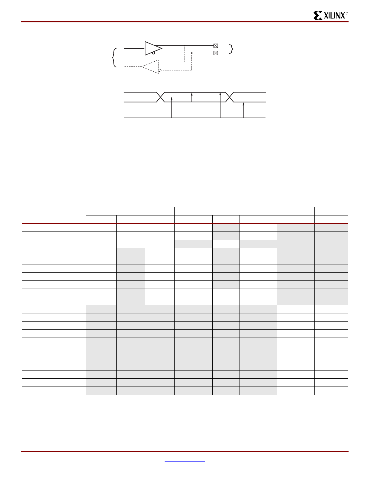
Timing Measurement Methodology
DC and Switching Characteristics
When measuring timing parameters at the programmable
I/Os, different signal standards call for different test
conditions. Ta bl e 2 5 lists the conditions to use for each
open connection, and V
measurement point (V
used at the Output.
is set to zero. The same
T
) that was used at the Input is also
M
standard.
V
(V
The method for measuring Input timing is as follows: A
signal that swings between a Low logic level of V
High logic level of V
is applied to the Input under test.
H
and a
L
Some standards also require the application of a bias
voltage to the V
pins of a given bank to properly set the
REF
input-switching threshold. The measurement point of the
Input signal (V
and V
.
H
) is commonly located halfway between VL
M
The Output test setup is shown in Figure 8. A termination
voltage V
is applied to the termination resistor RT, the other
T
end of which is connected to the Output. For each standard,
R
and VT generally take on the standard values
T
recommended for minimizing signal reflections. If the
T
FPGA Output
Notes:
1. The names shown in parentheses are
used in the IBIS file.
Figure 8:
Output Test Setup
)
REF
(R
R
T
V
(C
C
L
DS312-3_04_102406
REF
(V
M
REF
)
MEAS
)
)
standard does not ordinarily use terminations (for example,
LVCMOS, LVTTL), then R
Table 25:
Single-Ended
LVTTL - 0 3.3 1M 0 1.4
LV CM O S 33 - 0 3.3 1M 0 1.65
LV CM O S 25 - 0 2.5 1M 0 1.25
LV CM O S 18 - 0 1.8 1M 0 0.9
LV CM O S 15 - 0 1.5 1M 0 0.75
LV CM O S 12 - 0 1.2 1M 0 0.6
PCI33_3 Rising - Note 3 Note 3 25 0 0.94
PCI66_3 Rising - Note 3 Note 3 25 0 0.94
PCIX Rising - Note 3 Note 3 25 0 0.94
HSTL_I 0.75 V
HSTL_III 0.9 V
HSTL_I_18 0.9 V
HSTL_II_18 0.9 V
HSTL_III_18 1.1 V
SSTL18_I 0.9 V
SSTL18_II 0.9 V
SSTL2_I 1.25 V
SSTL2_II 1.25 V
Test Methods for Timing Measurement at I/Os
Signal Standard
(IOSTANDARD)
Falling 25 3.3 2.03
Falling 25 3.3 2.03
Falling 25 3.3 2.03
is set to 1MΩ to indicate an
T
Inputs Outputs
V
(V) VL (V) VH (V) RT (Ω) VT (V) VM (V)
REF
– 0.5 V
REF
– 0.5 V
REF
– 0.5 V
REF
– 0.5 V
REF
– 0.5 V
REF
– 0.5 V
REF
– 0.5 V
REF
– 0.75 V
REF
– 0.75 V
REF
+ 0.5 50 0.75 V
REF
+ 0.5 50 1.5 V
REF
+ 0.5 50 0.9 V
REF
+ 0.5 25 0.9 V
REF
+ 0.5 50 1.8 V
REF
+ 0.5 50 0.9 V
REF
+ 0.5 25 0.9 V
REF
+ 0.75 50 1.25 V
REF
+ 0.75 25 1.25 V
REF
Inputs and
Outputs
REF
REF
REF
REF
REF
REF
REF
REF
REF
DS610-3 (v2.0) July 16, 2007 www.xilinx.com 31
Product Specification
Page 32

DC and Switching Characteristics
R
Table 25:
SSTL3_I 1.5 V
SSTL3_II 1.5 V
Test Methods for Timing Measurement at I/Os
Signal Standard
(IOSTANDARD)
V
(V) VL (V) VH (V) RT (Ω)V
REF
Inputs Outputs
– 0.75 V
REF
– 0.75 V
REF
(Continued)
+ 0.75 50 1.5 V
REF
+ 0.75 25 1.5 V
REF
Differential
LVDS_25 -V
LVDS_33 -V
BLVDS_25 -V
MINI_LVDS_25 -V
MINI_LVDS_33 -V
LVPECL_25 -V
LVPECL_33 -V
RSDS_25 -V
RSDS_33 -V
TMDS_33 -V
PPDS_25 -V
PPDS_33 -V
DIFF_HSTL_I_18 0.9 V
DIFF_HSTL_II_18 0.9 V
DIFF_HSTL_III_18 1.1 V
DIFF_HSTL_I 0.9 V
DIFF_HSTL_III 0.9 V
DIFF_SSTL18_I 0.9 V
DIFF_SSTL18_II 0.9 V
DIFF_SSTL2_I 1.25 V
DIFF_SSTL2_II 1.25 V
DIFF_SSTL3_I 1.5 V
DIFF_SSTL3_II 1.5 V
– 0.125 V
ICM
– 0.125 V
ICM
– 0.125 V
ICM
– 0.125 V
ICM
– 0.125 V
ICM
– 0.3 V
ICM
– 0.3 V
ICM
– 0.1 V
ICM
– 0.1 V
ICM
– 0.1 V
ICM
– 0.1 V
ICM
– 0.1 V
ICM
– 0.5 V
REF
– 0.5 V
REF
– 0.5 V
REF
– 0.5 V
REF
– 0.5 V
REF
– 0.5 V
REF
– 0.5 V
REF
– 0.5 V
REF
– 0.5 V
REF
– 0.5 V
REF
– 0.5 V
REF
+ 0.125 50 1.2 V
ICM
+ 0.125 50 1.2 V
ICM
+ 0.125 1M 0 V
ICM
+ 0.125 50 1.2 V
ICM
+ 0.125 50 1.2 V
ICM
+ 0.3 N/A N/A V
ICM
+ 0.3 N/A N/A V
ICM
+ 0.1 50 1.2 V
ICM
+ 0.1 50 1.2 V
ICM
+ 0.1 50 3.3 V
ICM
+ 0.1 50 0.8 V
ICM
+ 0.1 50 0.8 V
ICM
+ 0.5 50 0.9 V
REF
+ 0.5 50 0.9 V
REF
+ 0.5 50 1.8 V
REF
+ 0.5 50 0.9 V
REF
+ 0.5 50 0.9 V
REF
+ 0.5 50 0.9 V
REF
+ 0.5 50 0.9 V
REF
+ 0.5 50 1.25 V
REF
+ 0.5 50 1.25 V
REF
+ 0.5 50 1.5 V
REF
+ 0.5 50 1.5 V
REF
Notes:
1. Descriptions of the relevant symbols are as follows:
V
– The reference voltage for setting the input switching threshold
REF
– The common mode input voltage
V
ICM
V
– Voltage of measurement point on signal transition
M
– Low-level test voltage at Input pin
V
L
V
– High-level test voltage at Input pin
H
– Effective termination resistance, which takes on a value of 1 MΩ when no parallel termination is required
R
T
V
– Termination voltage
T
2. The load capacitance (C
) at the Output pin is 0 pF for all signal standards.
L
3. According to the PCI specification.
Inputs and
Outputs
(V) VM (V)
T
REF
REF
ICM
ICM
ICM
ICM
ICM
ICM
ICM
ICM
ICM
ICM
ICM
ICM
REF
REF
REF
REF
REF
REF
REF
REF
REF
REF
REF
The capacitive load (CL) is connected between the output
and GND.
The Output timing for all standards, as published
from those measurements to produce the final timing
numbers as published in the speed files and data sheet.
in the speed files and the data sheet, is always based on a
C
value of zero.
L
High-impedance probes (less than 1 pF)
are used for all measurements. Any delay that the test
fixture might contribute to test measurements is subtracted
32 www.xilinx.com DS610-3 (v2.0) July 16, 2007
Product Specification
Page 33

R
Using IBIS Models to Simulate Load Conditions in Application
DC and Switching Characteristics
IBIS models permit the most accurate prediction of timing
delays for a given application. The parameters found in the
IBIS model (V
with the parameters used in Tabl e 2 5 (V
not confuse V
model with V
table. A fourth parameter, C
, R
REF
REF
REF
, and V
REF
(the termination voltage) from the IBIS
(the input-switching threshold) from the
REF
) correspond directly
MEAS
, RT, and VM). Do
T
, is always zero. The four
parameters describe all relevant output test conditions. IBIS
models are found in the Xilinx development software as well
as at the following link:
http://www.xilinx.com/xlnx/xil_sw_updates_home.jsp
Delays for a given application are simulated according to its
specific load conditions as follows:
1. Simulate the desired signal standard with the output
driver connected to the test setup shown in Figure 8.
Simultaneously Switching Output Guidelines
This section provides guidelines for the recommended
maximum allowable number of Simultaneous Switching
Outputs (SSOs). These guidelines describe the maximum
number of user I/O pins of a given output signal standard
that should simultaneously switch in the same direction,
while maintaining a safe level of switching noise. Meeting
these guidelines for the stated test conditions ensures that
the FPGA operates free from the adverse effects of ground
and power bounce.
Ground or power bounce occurs when a large number of
outputs simultaneously switch in the same direction. The
output drive transistors all conduct current to a common
voltage rail. Low-to-High transitions conduct to the V
rail; High-to-Low transitions conduct to the GND rail. The
resulting cumulative current transient induces a voltage
difference across the inductance that exists between the die
pad and the power supply or ground return. The inductance
is associated with bonding wires, the package lead frame,
and any other signal routing inside the package. Other
variables contribute to SSO noise levels, including stray
inductance on the PCB as well as capacitive loading at
receivers. Any SSO-induced voltage consequently affects
internal switching noise margins and ultimately signal
quality.
CCO
Use parameter values V
C
is zero.
REF
2. Record the time to V
, RT, and VM from Ta bl e 2 5.
T
.
M
3. Simulate the same signal standard with the output
driver connected to the PCB trace with load. Use the
appropriate IBIS model (including V
and V
values) or capacitive value to represent the
MEAS
REF
, R
REF
, C
REF
,
load.
4. Record the time to V
MEAS
.
5. Compare the results of steps 2 and 4. Add (or subtract)
the increase (or decrease) in delay to (or from) the
appropriate Output standard adjustment (Table 24) to
yield the worst-case delay of the PCB trace.
Generally, the left and right I/O banks (Banks 1 and 3)
support higher output drive current.
Multiply the appropriate numbers from Ta b l e 2 6 and
Tab le 2 7 to calculate the maximum number of SSOs
allowed within an I/O bank. Exceeding these SSO
guidelines might result in increased power or ground
bounce, degraded signal integrity, or increased system jitter.
SSO
/IO Bank = Table 26 x Ta bl e 2 7
MAX
The recommended maximum SSO values assumes that the
FPGA is soldered on the printed circuit board and that the
board uses sound design practices. The SSO values do not
apply for FPGAs mounted in sockets, due to the lead
inductance introduced by the socket.
Table 26:
XC3SD1800A 6 9
XC3SD3400A 6 10
Equivalent V
Device
/GND Pairs per Bank
CCO
Package Style
CS484 FG676
(including Pb-free)
Tab le 2 6 and Ta b l e 2 7 provide the essential SSO
guidelines. For each device/package combination, Ta b l e 26
provides the number of equivalent V
/GND pairs. For
CCO
each output signal standard and drive strength, Table 27
recommends the maximum number of SSOs, switching in
the same direction, allowed per V
/GND pair within an
CCO
I/O bank. The guidelines in Ta bl e 2 7 are categorized by
package style, slew rate, and output drive current.
Furthermore, the number of SSOs is specified by I/O bank.
DS610-3 (v2.0) July 16, 2007 www.xilinx.com 33
Product Specification
Page 34

DC and Switching Characteristics
R
Table 27:
Switching Outputs per V
Recommended Number of Simultaneously
CCO
Signal Standard
(IOSTANDARD)
Single-Ended Standards
LV TT L Sl ow 2
Fast 2
QuietIO 2
LVCMOS33 Slow 2
Fast 2
QuietIO 2
-GND Pair (V
Top, Bottom
(Banks 0,2)
4
6
8
12
16
24
4
6
8
12
16
24
4
6
8
12
16
24
4
6
8
12
16
24
4
6
8
12
16
24
4
6
8
12
16
24
=3.3V)
CCAUX
Package Type
CS484, FG676
Left, Right
(Banks 1,3)
60 60
41 41
29 29
22 22
13 13
11 11
99
10 10
66
55
33
33
33
22
80 80
48 48
36 36
27 27
16 16
13 13
12 12
76 76
46 46
27 27
20 20
13 13
10 10
–9
10 10
88
55
44
44
22
–2
76 76
46 46
32 32
26 26
18 18
14 14
–10
Table 27:
Switching Outputs per V
Recommended Number of Simultaneously
CCO
Signal Standard
(IOSTANDARD)
LVCMOS25 Slow 2
Fast 2
QuietIO 2
LVCMOS18 Slow 2
Fast 2
QuietIO 2
-GND Pair (V
Top, Bottom
(Banks 0,2)
4
6
8
12
16
24
4
6
8
12
16
24
4
6
8
12
16
24
4
6
8
12
16
4
6
8
12
16
4
6
8
12
16
=3.3V)
CCAUX
Package Type
CS484, FG676
Left, Right
(Banks 1,3)
76 76
46 46
33 33
24 24
18 18
–11
–7
18 18
14 14
66
66
33
–3
–2
76 76
60 60
48 48
36 36
36 36
–36
–8
64 64
34 34
22 22
18 18
–13
–10
18 18
99
77
44
–4
–3
64 64
64 64
48 48
36 36
–36
–24
34 www.xilinx.com DS610-3 (v2.0) July 16, 2007
Product Specification
Page 35

R
DC and Switching Characteristics
Table 27:
Switching Outputs per V
Recommended Number of Simultaneously
-GND Pair (V
CCO
CCAUX
=3.3V)
Package Type
CS484, FG676
Signal Standard
(IOSTANDARD)
LVCMOS15 Slow 2
Fast 2
QuietIO 2
LVCMOS12 Slow 2
Fast 2
QuietIO 2
PCI33_3
PCI66_3
PCIX
HSTL_I
HSTL_III
HSTL_I_18
HSTL_II_18
HSTL_III_18
SSTL18_I
SSTL18_II
SSTL2_I
SSTL2_II
SSTL3_I
SSTL3_II
Top, Bottom
4
6
8
12
4
6
8
12
4
6
8
12
4
6
4
6
4
6
(Banks 0,2)
55 55
31 31
18 18
–15
–10
25 25
10 10
66
–4
–3
70 70
40 40
31 31
–31
–20
40 40
–25
–18
31 31
–13
–9
55 55
–36
–36
16 16
–13
–11
–20
–8
17 17
–5
10 8
715
–3
18 18
–9
810
67
Left, Right
(Banks 1,3)
Differential Standards (Number of I/O Pairs or Channels)
LV DS _ 25
LV DS _ 33
BLVDS_25
MINI_LVDS_25
MINI_LVDS_33
LVPECL_25
22
27
–
–
44
22
27
Inputs Only
–
–
Table 27:
Switching Outputs per V
Recommended Number of Simultaneously
-GND Pair (V
CCO
CCAUX
=3.3V)
Package Type
CS484, FG676
Signal Standard
(IOSTANDARD)
LVPECL_33
RSDS_25
RSDS_33
TMDS_33
PPDS_25
PPDS_33
DIFF_HSTL_I_18
DIFF_HSTL_II_18
DIFF_HSTL_III_18
DIFF_HSTL_I
DIFF_HSTL_III
DIFF_SSTL18_I
DIFF_SSTL18_II
DIFF_SSTL2_I
DIFF_SSTL2_II
DIFF_SSTL3_I
DIFF_SSTL3_II
Top, Bottom
(Banks 0,2)
22
27
27
22
27
88
–2
54
–10
–4
37
–1
99
–4
45
33
Left, Right
(Banks 1,3)
Inputs Only
–
–
–
–
–
Notes:
1. Not all I/O standards are supported on all I/O banks. The left and
right banks (I/O banks 1 and 3) support higher output drive
current than the top and bottom banks (I/O banks 0 and 2).
Similarly, true differential output standards, such as LVDS,
RSDS, PPDS, miniLVDS, and TMDS, are only supported in top
or bottom banks (I/O banks 0 and 2). Refer to UG331
Generation FPGA User Guide
2. The numbers in this table are recommendations that assume
sound board lay out practice. This table assumes the following
parasitic factors: combined PCB trace and land inductance per
V
and GND pin of 1.0 nH, receiver capacitive load of 15 pF.
CCO
Test limits are the V
standard.
3. If more than one signal standard is assigned to the I/Os of a given
bank, refer to XAPP689
for information on how to perform weighted average SSO
FPGAs
calculations.
IL/VIH
for additional information.
voltage limits for the respective I/O
:
Managing Ground Bounce in Large
:
Spartan-3
DS610-3 (v2.0) July 16, 2007 www.xilinx.com 35
Product Specification
Page 36

DC and Switching Characteristics
Configurable Logic Block (CLB) Timing
R
Table 28:
CLB (SLICEM) Timing
Symbol Description
Clock-to-Output Times
T
CKO
When reading from the FFX (FFY) Flip-Flop, the time
from the active transition at the CLK input to data
appearing at the XQ (YQ) output
Setup Times
T
T
AS
DICK
Time from the setup of data at the F or G input to the
active transition at the CLK input of the CLB
Time from the setup of data at the BX or BY input to
the active transition at the CLK input of the CLB
Hold Times
T
T
AH
CKDI
Time from the active transition at the CLK input to the
point where data is last held at the F or G input
Time from the active transition at the CLK input to the
point where data is last held at the BX or BY input
Clock Timing
T
T
F
CH
CL
TOG
The High pulse width of the CLB’s CLK signal 0.63 –0.75–ns
The Low pulse width of the CLK signal 0.63 –0.75–ns
Toggle frequency (for export control) 0 770 0 667 MHz
Propagation Times
T
ILO
The time it takes for data to travel from the CLB’s F
(G) input to the X (Y) output
Set/Reset Pulse Width
T
RPW_CLB
The minimum allowable pulse width, High or Low, to
the CLB’s SR input
Speed Grade
-5 -4
Min Max Min Max
Units
–0.60–0.68ns
0.18 –0.36–ns
1.58 –1.88–ns
0.00 –0.00–ns
0.00 –0.00–ns
–0.62–0.71ns
1.33 –1.61–ns
Notes:
1. The numbers in this table are based on the operating conditions set forth in Ta b l e 7 .
36 www.xilinx.com DS610-3 (v2.0) July 16, 2007
Product Specification
Page 37

R
DC and Switching Characteristics
Table 29:
CLB Distributed RAM Switching Characteristics
Symbol Description
Clock-to-Output Times
T
SHCKO
Time from the active edge at the CLK input to data appearing on
the distributed RAM output
Setup Times
T
DS
T
AS
T
WS
Setup time of data at the BX or BY input before the active
transition at the CLK input of the distributed RAM
Setup time of the F/G address inputs before the active transition
at the CLK input of the distributed RAM
Setup time of the write enable input before the active transition at
the CLK input of the distributed RAM
Hold Times
T
DH
T
AH, TWH
Hold time of the BX and BY data inputs after the active transition
at the CLK input of the distributed RAM
Hold time of the F/G address inputs or the write enable input after
the active transition at the CLK input of the distributed RAM
Clock Pulse Width
T
WPH
, T
WPL
Minimum High or Low pulse width at CLK input 0.88 -1.01-ns
Speed Grade
-5 -4
Min Max Min Max
Units
-1.44-1.72ns
-0.07 --0.02-ns
0.18 -0.36-ns
0.30 -0.59-ns
0.13 -0.13-ns
0.01 -0.01-ns
Table 30:
CLB Shift Register Switching Characteristics
Symbol Description
Clock-to-Output Times
T
REG
Time from the active edge at the CLK input to data appearing on
the shift register output
Setup Times
T
SRLDS
Setup time of data at the BX or BY input before the active
transition at the CLK input of the shift register
Hold Times
T
SRLDH
Hold time of the BX or BY data input after the active transition at
the CLK input of the shift register
Clock Pulse Width
T
WPH
, T
WPL
Minimum High or Low pulse width at CLK input 0.90 -1.01-ns
Clock Buffer/Multiplexer Switching Characteristics
Table 31:
Global clock buffer (BUFG, BUFGMUX, BUFGCE) I input to
O-output delay
Global clock multiplexer (BUFGMUX) select S-input setup to I0 and
I1 inputs. Same as BUFGCE enable CE-input
Frequency of signals distributed on global buffers (all sides) F
Clock Distribution Switching Characteristics
Description Symbol Minimum
T
GIO
T
GSI
BUFG
-5 -4
UnitsMin Max Min Max
-4.11-4.82ns
0.13 -0.18-ns
0.16 -0.15-ns
Maximum
Speed Grade
-5 -4
Units
- 0.22 0.23 ns
- 0.56 0.63 ns
0350333MHz
DS610-3 (v2.0) July 16, 2007 www.xilinx.com 37
Product Specification
Page 38

DC and Switching Characteristics
Block RAM Timing
R
Table 32:
Block RAM Timing
Symbol Description
Clock-to-Output Times
T
RCKO_DOA_NC
When reading from block RAM, the delay from the active
transition at the CLK input to data appearing at the DOUT
output
T
RCKO_DOA
Clock CLK to DOUT output (with output register)
Setup Times
T
RCCK_ADDR
T
RDCK_DIB
T
RCCK_ENB
T
RCCK_WEB
T
RCCK_REGCE
Setup time for the ADDR inputs before the active transition
at the CLK input of the block RAM
Setup time for data at the DIN inputs before the active
transition at the CLK input of the block RAM
Setup time for the EN input before the active transition at the
CLK input of the block RAM
Setup time for the WE input before the active transition at the
CLK input of the block RAM
Setup time for the CE input before the active transition at the
CLK input of the block RAM
T
RCCK_RST
Setup time for the RST input before the active transition at
the CLK input of the block
Hold Times
T
RCKC_ADDR
T
RDCK_DIB
T
RCKC_ENB
T
RCKC_WEB
T
RCKC_REGCE
Hold time on the ADDR inputs after the active transition at
the CLK input
Hold time on the DIN inputs after the active transition at the
CLK input
Hold time on the EN input after the active transition at the
CLK input
Hold time on the WE input after the active transition at the
CLK input
Hold time on the CE input after the active transition at the
CLK input
T
RCKC_RST
Hold time on the RST input after the active transition at the
CLK input
Clock Timing
T
BPWH
T
BPWL
High pulse width of the CLK signal 1.56 -1.79-ns
Low pulse width of the CLK signal 1.56 -1.79-ns
Clock Frequency
F
BRAM
Block RAM clock frequency. 0 320 0 280 MHz
Notes:
1. The numbers in this table are based on the operating conditions set forth in Ta b l e 7 .
Speed Grade
-5 -4
Min Max Min Max
Units
-2.38-2.80ns
-1.24-1.45ns
0.40 -0.46-ns
0.29 -0.33-ns
0.51 -0.60-ns
0.64 -0.75-ns
0.34
0.22
-0.40-ns
-0.25-ns
0.09 -0.10-ns
0.09 -0.10-ns
0.09 -0.10-ns
0.09 -0.10-ns
0.09
0.09
-0.10-ns
-0.10-ns
38 www.xilinx.com DS610-3 (v2.0) July 16, 2007
Product Specification
Page 39

R
DSP48A Timing
DC and Switching Characteristics
To reference the DSP48A block diagram, see the
Table 33:
Setup Times for the DSP48A
XtremeDSP DSP48A for Spartan-3A DSP FPGA User Guide
Symbol Description Preadder Multiplier Postadder
Setup Times of Data/Control Pins to the Input Register Clock
T
DSPDCK_AA
T
DSPDCK_DB
T
DSPDCK_CC
T
DSPDCK_DD
T
DSPDCK_OPB
T
DSPDCK_OPOP
A input to A register CLK - - - 0.04 0.04 ns
D input to B register CLK Yes - - 1.64 1.88 ns
C input to C register CLK - - - 0.05 0.05 ns
D input to D register CLK - - - 0.04 0.04 ns
OPMODE input to B register CLK Yes - - 0.37 0.42 ns
OPMODE input to OPMODE register CLK - - - 0.06 0.06 ns
Setup Times of Data Pins to the Pipeline Register Clock
T
DSPDCK_AM
T
DSPDCK_BM
A input to M register CLK -Yes- 3.30 3.79 ns
B input to M register CLK Yes Yes - 4.33 4.97 ns
No Yes
T
DSPDCK_DM
T
DSPDCK_OPM
D input to M register CLK Yes Yes - 4.41 5.06 ns
OPMODE to M register CLK Yes Yes - 4.72 5.42 ns
Setup Times of Data/Control Pins to the Output Register Clock
T
DSPDCK_AP
T
DSPDCK_BP
A input to P register CLK - Yes Yes 4.78 5.49 ns
B input to P register CLK Yes Yes Yes 5.87 6.74 ns
No Yes Yes 4.77 5.48 ns
T
DSPDCK_DP
T
DSPDCK_CP
T
DSPDCK_OPP
D input to P register CLK Yes Yes Yes 5.95 6.83 ns
C input to P register CLK - - Yes 1.90 2.18 ns
OPMODE input to P register CLK Yes Yes Yes 6.25 7.18 ns
(UG431).
Speed Grade
-5 -4
Min Min
- 3.30 3.79 ns
Units
DS610-3 (v2.0) July 16, 2007 www.xilinx.com 39
Product Specification
Page 40

DC and Switching Characteristics
R
Table 34:
Clock to Out, Propagation Delays, and Maximum Frequency for the DSP48A
Symbol Description Preadder Multiplier Postadder
Clock to Out from Output Register Clock to Output Pin
T
DSPCKO_PP
CLK (PREG) to P output - - - 1.26 1.44 ns
Clock to Out from Pipeline Register Clock to Output Pins
T
DSPCKO_PM
CLK (MREG) to P output -YesYes3.163.63ns
- Yes No 1.94 2.23 ns
Clock to Out from Input Register Clock to Output Pins
T
DSPCKO_PA
T
DSPCKO_PB
T
DSPCKO_PC
T
DSPCKO_PD
CLK (AREG) to P output -YesYes6.337.27ns
CLK (BREG) to P output Yes Yes Yes 7.45 8.56 ns
CLK (CREG) to P output - - Yes 3.37 3.87 ns
CLK (DREG) to P output Yes Yes Yes 7.33 8.42 ns
Combinatorial Delays from Input Pins to Output Pins
T
DSPDO_AP
T
DSPDO_BP
A or B input to P output - No Yes 2.78 3.19 ns
- Yes No 4.59 5.28 ns
-YesYes5.656.49ns
T
DSPDO_BP
B input to P output Yes No No 3.49 4.01 ns
Yes Yes No 5.79 6.65 ns
Ye s Ye s Ye s 6 . 7 4 7 . 7 4 n s
T
DSPDO_CP
T
DSPDO_DP
T
DSPDO_OPP
C input to P output - - Yes 2.76 3.17 ns
D input to P output Yes Yes Yes 6.81 7.82 ns
OPMODE input to P output Yes Yes Yes 7.12 8.18 ns
Maximum Frequency
F
MAX
All registers used Yes Yes Yes 287 250 MHz
A1REG or B1REG to PREG
- Yes No 246 214 MHz
- Yes Yes 195 170 MHz
DREG, A0REG, or B0REG to MREG Yes Yes
Speed Grade
-5 -4
Max Max
Units
- 205 178 MHz
40 www.xilinx.com DS610-3 (v2.0) July 16, 2007
Product Specification
Page 41

R
Digital Clock Manager (DCM) Timing
DC and Switching Characteristics
For specification purposes, the DCM consists of three key
components: the Delay-Locked Loop (DLL), the Digital
Frequency Synthesizer (DFS), and the Phase Shifter (PS).
Aspects of DLL operation play a role in all DCM
applications. All such applications inevitably use the CLKIN
and the CLKFB inputs connected to either the CLK0 or the
CLK2X feedback, respectively. Thus, specifications in the
DLL tables (Tab l e 3 5 and Ta bl e 3 6 ) apply to any application
that only employs the DLL component. When the DFS
and/or the PS components are used together with the DLL,
then the specifications listed in the DFS and PS tables
(Ta b l e 3 7 through Ta b l e 4 0 ) supersede any corresponding
ones in the DLL tables. DLL specifications that do not
change with the addition of DFS or PS functions are
presented in Ta bl e 3 5 and Ta b l e 3 6 .
Period jitter and cycle-cycle jitter are two of many different
ways of specifying clock jitter. Both specifications describe
statistical variation from a mean value.
Period jitter is the worst-case deviation from the ideal clock
period over a collection of millions of samples. In a
histogram of period jitter, the mean value is the clock period.
Cycle-cycle jitter is the worst-case difference in clock period
between adjacent clock cycles in the collection of clock
periods sampled. In a histogram of cycle-cycle jitter, the
mean value is zero.
Delay-Locked Loop (DLL)
Table 35:
Input Frequency Ranges
F
CLKIN
Input Pulse Requirements
CLKIN_PULSE CLKIN pulse width as a
Input Clock Jitter Tolerance and Delay Path Variation
CLKIN_CYC_JITT_DLL_LF Cycle-to-cycle jitter at the
CLKIN_CYC_JITT_DLL_HF F
CLKIN_PER_JITT_DLL Period jitter at the CLKIN input
CLKFB_DELAY_VAR_EXT Allowable variation of off-chip feedback delay from
Recommended Operating Conditions for the DLL
Symbol Description
CLKIN_FREQ_DLL Frequency of the CLKIN clock input 5
F
< 150 MHz 40% 60% 40% 60% percentage of the CLKIN
period
(4)
CLKIN input
the DCM output to the CLKFB input
CLKIN
F
> 150 MHz 45% 55% 45% 55% -
CLKIN
F
< 150 MHz - ±300 -±300ps
CLKIN
> 150 MHz - ±150 -±150ps
CLKIN
Speed Grade
-5 -4
(3)
Units
MHz
Min Max Min Max
(2)
-±1-±1ns
-±1-±1ns
280
(3)
(2)
5
250
Notes:
1. DLL specifications apply when any of the DLL outputs (CLK0, CLK90, CLK180, CLK270, CLK2X, CLK2X180, or CLKDV) are in use.
2. The DFS, when operating independently of the DLL, supports lower FCLKIN frequencies. See Ta b l e 3 7 .
3. To support double the maximum effective FCLKIN limit, set the CLKIN_DIVIDE_BY_2 attribute to TRUE. This attribute divides the incoming
clock period by two as it enters the DCM. The CLK2X output reproduces the clock frequency provided on the CLKIN input.
4. CLKIN input jitter beyond these limits might cause the DCM to lose lock.
5. The DCM specifications are guaranteed when both adjacent DCMs are locked
DS610-3 (v2.0) July 16, 2007 www.xilinx.com 41
Product Specification
Page 42

DC and Switching Characteristics
R
Table 36:
Switching Characteristics for the DLL
Speed Grade
-5 -4
Symbol Description Device
Min Max Min Max
Units
Output Frequency Ranges
CLKOUT_FREQ_CLK0 Frequency for the CLK0 and CLK180 outputs All 5 280 5 250 MHz
CLKOUT_FREQ_CLK90 Frequency for the CLK90 and CLK270 outputs 5 200 5 200 MHz
CLKOUT_FREQ_2X Frequency for the CLK2X and CLK2X180 outputs 10 334 10 334 MHz
CLKOUT_FREQ_DV Frequency for the CLKDV output 0.3125 186 0.3125 166 MHz
Output Clock Jitter
(2,3,4)
CLKOUT_PER_JITT_0 Period jitter at the CLK0 output All - ±100 - ±100 ps
CLKOUT_PER_JITT_90 Period jitter at the CLK90 output
CLKOUT_PER_JITT_180 Period jitter at the CLK180 output
CLKOUT_PER_JITT_270 Period jitter at the CLK270 output
CLKOUT_PER_JITT_2X Period jitter at the CLK2X and CLK2X180 outputs
CLKOUT_PER_JITT_DV1 Period jitter at the CLKDV output when performing integer
division
CLKOUT_PER_JITT_DV2 Period jitter at the CLKDV output when performing non-integer
division
Duty Cycle
(4)
CLKOUT_DUTY_CYCLE_DLL Duty cycle variation for the CLK0, CLK90, CLK180, CLK270,
CLK2X, CLK2X180, and CLKDV outputs, including the
BUFGMUX and clock tree duty-cycle distortion
Phase Alignment
(4)
All
- ±150 - ±150 ps
- ±150 - ±150 ps
- ±150 - ±150 ps
- ±[0.5%
of CLKIN
period
+ 100]
- ±[0.5%
of CLKIN
period
+ 100]
- ±150 - ±150 ps
- ±[0.5%
of CLKIN
period
+ 100]
-±[1% of
CLKIN
period
+ 350]
- ±[0.5%
of CLKIN
period
+ 100]
-±[1% of
CLKIN
period
+ 350]
CLKIN_CLKFB_PHASE Phase offset between the CLKIN and CLKFB inputs All - ±150 - ±150 ps
CLKOUT_PHASE_DLL Phase offset between DLL outputs
CLK0 to CLK2X
(not CLK2X180)
All others
-±[1% of
CLKIN
period
+ 100]
-±[1% of
CLKIN
period
+ 150]
-±[1% of
CLKIN
period
+ 100]
-±[1% of
CLKIN
period
+ 150]
Lock Time
LOCK_DLL
(3)
When using the DLL alone: The
time from deassertion at the DCM’s
Reset input to the rising transition
at its LOCKED output. When the
5 MHz <
F
CLKIN
F
< 15 MHz All -5-5ms
CLKIN
> 15 MHz - 600 - 600 μs
DCM is locked, the CLKIN and
CLKFB signals are in phase
Delay Lines
DCM_DELAY_STEP
(5)
Finest delay resolution, averaged over all steps All 15 35 15 35 ps
ps
ps
ps
ps
ps
Notes:
1. The numbers in this table are based on the operating conditions set forth in Ta b l e 7 and Table 35.
2. Indicates the maximum amount of output jitter that the DCM adds to the jitter on the CLKIN input.
3. For optimal jitter tolerance and faster lock time, use the CLKIN_PERIOD attribute.
4. Some jitter and duty-cycle specifications include 1% of input clock period or 0.01 UI. For example, the data sheet specifies a maximum jitter of “±[1%
of CLKIN period + 150]”. Assume the CLKIN frequency is 100 MHz. The equivalent CLKIN period is 10 ns and 1% of 10 ns is 0.1 ns or 100 ps.
According to the data sheet, the maximum jitter is ±[100 ps + 150 ps] = ±250 ps
5. The typical delay step size is 23 ps.
, averaged over all steps.
42 www.xilinx.com DS610-3 (v2.0) July 16, 2007
Product Specification
Page 43
R
DC and Switching Characteristics
Digital Frequency Synthesizer (DFS)
Table 37:
Input Frequency Ranges
F
CLKIN
Input Clock Jitter Tolerance
CLKIN_CYC_JITT_FX_LF Cycle-to-cycle jitter at the CLKIN
CLKIN_CYC_JITT_FX_HF F
CLKIN_PER_JITT_FX Period jitter at the CLKIN input
Notes:
1. DFS specifications apply when either of the DFS outputs (CLKFX or CLKFX180) are used.
2. If both DFS and DLL outputs are used on the same DCM, follow the more restrictive CLKIN_FREQ_DLL specifications in Table 35.
3. CLKIN input jitter beyond these limits may cause the DCM to lose lock.
4. The DCM specifications are guaranteed when both adjacent DCMs are locked
Recommended Operating Conditions for the DFS
Speed Grade
-5 -4
Symbol Description
(2)
CLKIN_FREQ_FX Frequency for the CLKIN input 0.2 333 0.2 333 MHz
(3)
F
< 150 MHz - ±300 -±300ps
input, based on CLKFX output
frequency
CLKFX
> 150 MHz - ±150 -±150ps
CLKFX
Min Max Min Max
-±1-±1ns
Units
Table 38:
Output Frequency Ranges
CLKOUT_FREQ_FX
Output Clock Jitter
CLKOUT_PER_JITT_FX Period jitter at the CLKFX and CLKFX180
Switching Characteristics for the DFS
Symbol Description Device
(2)
(3,4)
Frequency for the CLKFX and CLKFX180 outputs All 5 350 5 311 MHz
outputs.
CLKIN
≤ 20 MHz
All Typ Max Typ Max
Speed Grade
-5 -4
Min Max Min Max
Use the Spartan-3A Jitter Calculator:
www.xilinx.com/bvdocs/publications/
Units
ps
s3a_jitter_calc.zip
CLKIN
> 20 MHz
Duty Cycle
CLKOUT_DUTY_CYCLE_FX Duty cycle precision for the CLKFX and CLKFX180 outputs,
Phase Alignment
CLKOUT_PHASE_FX Phase offset between the DFS CLKFX output and the DLL CLK0
CLKOUT_PHASE_FX180 Phase offset between the DFS CLKFX180 output and the DLL
Lock Time
LOCK_FX
Notes:
1. The numbers in this table are based on the operating conditions set forth in Ta b l e 7 and Table 37.
2. DFS performance requires the additional logic automatically added by ISE 9.1i and later software revisions.
3. For optimal jitter tolerance and faster lock time, use the CLKIN_PERIOD attribute.
4. Maximum output jitter is characterized within a reasonable noise environment (40 SSOs and 25% CLB switching) on an FPGA. Output jitter strongly
5. The CLKFX and CLKFX180 outputs always have an approximate 50% duty cycle.
6. Some duty-cycle and alignment specifications include a percentage of the CLKFX output period. For example, the data sheet specifies a maximum
(5,6)
including the BUFGMUX and clock tree duty-cycle distortion
(6)
output when both the DFS and DLL are used
CLK0 output when both the DFS and DLL are used
(2,3)
depends on the environment, including the number of SSOs, the output drive strength, CLB utilization, CLB switching activities, switching frequency,
power supply and PCB design. The actual maximum output jitter depends on the system application.
CLKFX jitter of “±[1% of CLKFX period + 200]”. Assume the CLKFX output frequency is 100 MHz. The equivalent CLKFX period is 10 ns and 1% of
10 ns is 0.1 ns or 100 ps. According to the data sheet, the maximum jitter is ±[100 ps + 200 ps] = ±300 ps.
The time from deassertion at the DCM’s
Reset input to the rising transition at its
LOCKED output. The DFS asserts LOCKED
when the CLKFX and CLKFX180 signals are
valid. If using both the DLL and the DFS, use
the longer locking time.
F
5 MHz <
<
15 MHz
F
> 15 MHz - 450 - 450 μs
CLKIN
CLKIN
±[1% of
CLKFX
period
+ 100]
All -±[1% of
All - ±200 - ±200 ps
All -±[1% of
All
±[1% of
CLKFX
period
+ 200]
CLKFX
period
+ 350]
CLKFX
period
+ 200]
-5-5ms
±[1% of
CLKFX
period
+ 100]
-±[1% of
-±[1% of
±[1% of
CLKFX
period
+ 200]
CLKFX
period
+ 350]
CLKFX
period
+ 200]
ps
ps
ps
DS610-3 (v2.0) July 16, 2007 www.xilinx.com 43
Product Specification
Page 44

DC and Switching Characteristics
Phase Shifter (PS)
Table 39:
Operating Frequency Ranges
PSCLK_FREQ
(F
PSCLK
Input Pulse Requirements
PSCLK_PULSE PSCLK pulse width as a percentage of the PSCLK period 40% 60% 40% 60%
Recommended Operating Conditions for the PS in Variable Phase Mode
Symbol Description
Frequency for the PSCLK input 1 167 1 167 MHz
)
Speed Grade
-5 -4
Min Max Min Max
R
Units
-
Table 40:
Switching Characteristics for the PS in Variable Phase Mode
Symbol Description Phase Shift Amount Units
Phase Shifting Range
MAX_STEPS
(2)
Maximum allowed number of
DCM_DELAY_STEP steps for a given
CLKIN clock period, where T = CLKIN
clock period in ns. If using
CLKIN < 60 MHz
≥ 60 MHz
CLKIN
±[INTEGER(10 • (T
±[INTEGER(15 • (T
– 3 ns))] steps
CLKIN
– 3 ns))]
CLKIN
CLKIN_DIVIDE_BY_2 = TRUE,
double the clock effective clock
period.
FINE_SHIFT_RANGE_MIN Minimum guaranteed delay for variable phase shifting ±[MAX_STEPS •
ns
DCM_DELAY_STEP_MIN]
FINE_SHIFT_RANGE_MAX Maximum guaranteed delay for variable phase shifting ±[MAX_STEPS •
ns
DCM_DELAY_STEP_MAX]
Notes:
1. The numbers in this table are based on the operating conditions set forth in Tab l e 7 and Table 39.
2. The maximum variable phase shift range, MAX_STEPS, is only valid when the DCM is has no initial fixed phase shifting, that is, the
PHASE_SHIFT attribute is set to 0.
3. The DCM_DELAY_STEP values are provided at the bottom of Tab l e 3 6 .
Miscellaneous DCM Timing
Table 41:
DCM_RST_PW_MIN Minimum duration of a RST pulse width 3
Miscellaneous DCM Timing
Symbol Description Min Max Units
-CLKIN
cycles
44 www.xilinx.com DS610-3 (v2.0) July 16, 2007
Product Specification
Page 45

R
DC and Switching Characteristics
DNA Port Timing
Table 42:
T
Notes:
1. The minimum READ pulse width is 5 ns, and the maximum READ pulse width is 10 μs.
DNA_PORT Interface Timing
Symbol Description Min Max Units
T
DNASSU
T
DNASH
T
DNADSU
T
DNADH
T
DNARSU
T
DNARH
DNADCKO
T
DNACLKF
T
DNACLKL
T
DNACLKH
Setup time on SHIFT before the rising edge of CLK 1.0 –ns
Hold time on SHIFT after the rising edge of CLK 0.5 –ns
Setup time on DIN before the rising edge of CLK 1.0 –ns
Hold time on DIN after the rising edge of CLK 0.5 –ns
Setup time on READ before the rising edge of CLK 5.0 10,000 ns
Hold time on READ after the rising edge of CLK 0.0 –ns
Clock-to-output delay on DOUT after rising edge of CLK 0.5 1.5 ns
CLK frequency 0.0 100 MHz
CLK High time 1.0 ∞ ns
CLK Low time 1.0 ∞ ns
DS610-3 (v2.0) July 16, 2007 www.xilinx.com 45
Product Specification
Page 46

DC and Switching Characteristics
Suspend Mode Timing
R
SUSPEND Input
AWAKE Output
Flip-Flops, Block RAM,
Distributed RAM
FPGA Outputs
FPGA Inputs,
Interconnect
Table 43:
Suspend Mode Timing Parameters
Symbol Description Min Typ Max Units
Entering Suspend Mode
Entering Suspend Mode Exiting Suspend Mode
sw_gwe_cycle
sw_gts_cycle
t
SUSPENDHIGH_AWAKE
t
SUSPEND_GWE
t
SUSPENDLOW_AWAKE
Write Protected
t
SUSPEND_GTS
Defined by SUSPEND constraint
t
SUSPEND_DISABLE
t
SUSPEND_ENABLE
Blocked
Figure 9:
Suspend Mode Timing
t
AWAKE_GWE
t
AWAKE_GTS
DS610-3_08_061207
T
SUSPENDHIGH_AWAKE
T
SUSPENDFILTER
T
SUSPEND_GWE
T
SUSPEND_GTS
T
SUSPEND_DISABLE
Exiting Suspend Mode
T
SUSPENDLOW_AWAKE
T
SUSPEND_ENABLE
T
AWAKE_GWE1
T
AWAKE_GWE512
T
AWAKE_GTS1
T
AWAKE_GTS512
Rising edge of SUSPEND pin to falling edge of AWAKE pin without glitch filter
(
suspend_filter:No
)
Adjustment to SUSPEND pin rising edge parameters when glitch filter
enabled (
suspend_filter:Yes
)
Rising edge of SUSPEND pin until FPGA output pins drive their defined
SUSPEND constraint behavior
Rising edge of SUSPEND pin to write-protect lock on all writable clocked
elements
Rising edge of the SUSPEND pin to FPGA input pins and interconnect
disabled
Falling edge of the SUSPEND pin to rising edge of the AWAKE pin. Does not
include DCM lock time.
Falling edge of the SUSPEND pin to FPGA input pins and interconnect
re-enabled
Rising edge of the AWAKE pin until write-protect lock released on all writable
clocked elements, using
sw_clk:InternalClock
and
sw_gwe_cycle:1
.
Rising edge of the AWAKE pin until write-protect lock released on all writable
clocked elements, using
sw_clk:InternalClock
and
sw_gwe_cycle:512
.
Rising edge of the AWAKE pin until outputs return to the behavior described
in the FPGA application, using
sw_clk:InternalClock
and
sw_gts_cycle:1
Rising edge of the AWAKE pin until outputs return to the behavior described
in the FPGA application, using
sw_gts_cycle:512
.
sw_clk:InternalClock
and
–7–ns
+160 +300 +600 ns
–10–ns
–<5–ns
–340–ns
– 4 to 108 – μs
– 3.7 to 109 – μs
–67–ns
–14– μs
–57–ns
.
–14– μs
Notes:
1. These parameters based on characterization.
:
2. For information on using the Spartan-3A DSP Suspend feature, see XAPP480
Using Suspend Mode in Spartan-3 Generation FPGAs
.
46 www.xilinx.com DS610-3 (v2.0) July 16, 2007
Product Specification
Page 47

R
Configuration and JTAG Timing
General Configuration Power-On/Reconfigure Timing
DC and Switching Characteristics
V
V
CCO
CCINT
(Supply)
V
CCAUX
(Supply)
Bank 2
(Supply)
1.0V
2.0V
1.0V
T
POR
PROG_B
(Input)
T
PL
INIT_B
T
PROG
(Open-Drain)
CCLK
(Output)
Notes:
1. The V
CCINT
, V
CCAUX
, and V
supplies can be applied in any order.
CCO
2. The Low-going pulse on PROG_B is optional after power-on but necessary for reconfiguration without a power cycle.
3. The rising edge of INIT_B samples the voltage levels applied to the mode pins (M0 - M2).
Table 44:
Figure 10:
Power-On Timing and the Beginning of Configuration
Waveforms for Power-On and the Beginning of Configuration
Symbol Description Device
T
POR
(2)
The time from the application of V
Bank 2 supply voltage ramps (whichever occurs last) to the
CCINT
, V
CCAUX
, and V
CCO
rising transition of the INIT_B pin
T
PROG
T
PL
T
INIT
T
ICCK
(2)
(3)
The width of the low-going pulse on the PROG_B pin All 0.5 - μs
The time from the rising edge of the PROG_B pin to the
rising transition on the INIT_B pin
Minimum Low pulse width on INIT_B output All 300 -ns
The time from the rising edge of the INIT_B pin to the
generation of the configuration clock signal at the CCLK
output pin
T
ICCK
All -18ms
XC3SD1800A
XC3SD3400A
All 0.5 4 μs
1.2V
2.5V
or
3.3V
DS529-3_01_112906
All Speed Grades
UnitsMin Max
-2ms
-2ms
Notes:
1. The numbers in this table are based on the operating conditions set forth in Ta bl e 7 . This means power must be applied to all V
and V
CCAUX
lines.
CCINT
, V
CCO
2. Power-on reset and the clearing of configuration memory occurs during this period.
3. This specification applies only to the Master Serial, SPI, and BPI modes.
DS610-3 (v2.0) July 16, 2007 www.xilinx.com 47
Product Specification
,
Page 48

DC and Switching Characteristics
Configuration Clock (CCLK) Characteristics
Table 45:
Symbol Description
T
CCLK1
T
CCLK3
T
CCLK6
T
CCLK7
T
CCLK8
T
CCLK10
T
CCLK12
T
CCLK13
T
CCLK17
T
CCLK22
T
CCLK25
T
CCLK27
T
CCLK33
T
CCLK44
T
CCLK50
T
CCLK100
Master Mode CCLK Output Period by
ConfigRate
CCLK clock period by
ConfigRate
setting
(power-on value)
ConfigRate
Setting
1
3
6
7
8
10
12
13
17
22
25
27
33
44
50
100
Option Setting
Temperature
Range Minimum Maximum Units
Commercial 1,254
Industrial 1,180 ns
Commercial 413
Industrial 390 ns
Commercial 207
Industrial 195 ns
Commercial 178
Industrial 168 ns
Commercial 156
Industrial 147 ns
Commercial 123
Industrial 116 ns
Commercial 103
Industrial 97 ns
Commercial 93
Industrial 88 ns
Commercial 72
Industrial 68 ns
Commercial 54
Industrial 51 ns
Commercial 47
Industrial 45 ns
Commercial 44
Industrial 42 ns
Commercial 36
Industrial 34 ns
Commercial 26
Industrial 25 ns
Commercial 22
Industrial 21 ns
Commercial 11.2
Industrial 10.6 ns
2,000
667
334
286
250
200
167
154
118
91
80
75
61
46
40
20
R
ns
ns
ns
ns
ns
ns
ns
ns
ns
ns
ns
ns
ns
ns
ns
ns
Notes:
1. Set the
ConfigRate
option value when generating a configuration bitstream.
48 www.xilinx.com DS610-3 (v2.0) July 16, 2007
Product Specification
Page 49

R
DC and Switching Characteristics
Table 46:
Master Mode CCLK Output Frequency by
Symbol Description
F
CCLK1
F
CCLK3
F
CCLK6
F
CCLK7
F
CCLK8
F
CCLK10
F
CCLK12
F
CCLK13
F
CCLK17
F
CCLK22
F
CCLK25
F
CCLK27
F
CCLK33
F
CCLK44
F
CCLK50
F
CCLK100
Equivalent CCLK clock frequency
by
ConfigRate
setting
ConfigRate
ConfigRate
Setting
1
(power-on value)
3
6
7
8
10
12
13
17
22
25
27
33
44
50
100
Option Setting
Temperature
Range Minimum Maximum Units
Commercial
Industrial 0.847 MHz
Commercial
Industrial 2.57 MHz
Commercial
Industrial 5.13 MHz
Commercial
Industrial 5.96 MHz
Commercial
Industrial 6.81 MHz
Commercial
Industrial 8.63 MHz
Commercial
Industrial 10.31 MHz
Commercial
Industrial 11.37 MHz
Commercial
Industrial 14.61 MHz
Commercial
Industrial 19.61 MHz
Commercial
Industrial 22.23 MHz
Commercial
Industrial 23.81 MHz
Commercial
Industrial 29.23 MHz
Commercial
Industrial 40.00 MHz
Commercial
Industrial 47.66 MHz
Commercial
Industrial 94.34 MHz
0.400
1.20
2.40
2.80
3.20
4.00
4.80
5.20
6.80
8.80
10.00
10.80
13.20
17.60
20.00
40.00
0.797 MHz
2.42 MHz
4.83 MHz
5.61 MHz
6.41 MHz
8.12 MHz
9.70 MHz
10.69 MHz
13.74 MHz
18.44 MHz
20.90 MHz
22.39 MHz
27.48 MHz
37.60 MHz
44.80 MHz
88.68 MHz
Table 47:
Symbol Description
T
MCCL,
T
MCCH
Table 48:
Master Mode CCLK Output Minimum Low and High Time
Master Mode
CCLK
Minimum Low
and High Time
Commercial
Industrial
595 196 98.3 84.5 74.1 58.4 48.9 44.1 34.2 25.6 22.3 20.9 17.1 12.3 10.4 5.3
560 185 92.6 79.8 69.8 55.0 46.0 41.8 32.3 24.2 21.4 20.0 16.2 11.9 10.0 5.0
Slave Mode CCLK Input Low and High Time
ConfigRate
Setting
Units1 3 6 7 8 10121317222527334450100
ns
ns
Symbol Description Min Max Units
T
SCCL,
T
SCCH
CCLK Low and High time 5
∞
ns
DS610-3 (v2.0) July 16, 2007 www.xilinx.com 49
Product Specification
Page 50

DC and Switching Characteristics
Master Serial and Slave Serial Mode Timing
PROG_B
(Input)
INIT_B
(Open-Drain)
CCLK
(Input/Output)
T
DCC
R
CCSER
T
T
MCCH
SCCH
T
MCCL
T
SCCL
T
CCD
1/F
DIN
(Input)
DOUT
(Output)
Table 49:
Figure 11:
Timing for the Master Serial and Slave Serial Configuration Modes
Waveforms for Master Serial and Slave Serial Configuration
Symbol Description
Clock-to-Output Times
T
CCO
The time from the falling transition on the CCLK pin to data appearing at the
DOUT pin
Setup Times
T
DCC
The time from the setup of data at the DIN pin to the rising transition at the
CCLK pin
Hold Times
T
CCD
The time from the rising transition at the CCLK pin to the point when data is
last held at the DIN pin
Clock Timing
T
CCH
T
CCL
F
CCSER
High pulse width at the CCLK input pin Master See Ta bl e 47
Low pulse width at the CCLK input pin Master See Ta bl e 4 7
Frequency of the clock signal at the
CCLK input pin
Bit n+1
Slave/
Master
Bit n
T
CCO
Bit n-64
Bit n-63
All Speed Grades
DS312-3_05_103105
UnitsMin Max
Bit 0 Bit 1
Both 1.5 10 ns
Both 7 -ns
Master
Slave
0.0
1.0
-ns
Slave See Ta b le 48
Slave See Ta b le 48
No bitstream compression Slave 0 100 MHz
With bitstream compression 0 100 MHz
Notes:
1. The numbers in this table are based on the operating conditions set forth in Ta b l e 7 .
2. For serial configuration with a daisy-chain of multiple FPGAs, the maximum limit is 25 MHz.
50 www.xilinx.com DS610-3 (v2.0) July 16, 2007
Product Specification
Page 51

R
Slave Parallel Mode Timing
PROG_B
(Input)
INIT_B
(Open-Drain)
CSI_B
(Input)
RDWR_B
(Input)
CCLK
(Input)
T
SMCCW
T
SMDCC
T
SMCSCC
T
SMCCD
DC and Switching Characteristics
T
SMCCCS
T
SMWCC
T
MCCH
T
SCCH
1/F
CCPAR
T
T
MCCL
SCCL
D0 - D7
(Inputs)
Notes:
Byte 0 Byte 1 Byte n Byte n+1
DS529-3_02_051607
1. It is possible to abort configuration by pulling CSI_B Low in a given CCLK cycle, then switching RDWR_B Low or High in any subsequent
cycle for which CSI_B remains Low. The RDWR_B pin asynchronously controls the driver impedance of the D0 - D7 bus. When RDWR_B
switches High, be careful to avoid contention on the D0 - D7 bus.
Table 50:
Figure 12:
Timing for the Slave Parallel Configuration Mode
Waveforms for Slave Parallel Configuration
All Speed Grades
Symbol Description
UnitsMin Max
Setup Times
SMDCC
SMCSCC
SMCCW
(2)
The time from the setup of data at the D0-D7 pins to the rising transition at the CCLK pin 7 -ns
Setup time on the CSI_B pin before the rising transition at the CCLK pin 7 -ns
Setup time on the RDWR_B pin before the rising transition at the CCLK pin 17 -ns
T
T
T
Hold Times
T
SMCCD
T
SMCCCS
T
SMWCC
The time from the rising transition at the CCLK pin to the point when data is last held at
the D0-D7 pins
The time from the rising transition at the CCLK pin to the point when a logic level is last
held at the CSO_B pin
The time from the rising transition at the CCLK pin to the point when a logic level is last
held at the RDWR_B pin
1 -ns
0 -ns
0 -ns
Clock Timing
T
CCH
T
CCL
F
CCPAR
The High pulse width at the CCLK input pin 5 -ns
The Low pulse width at the CCLK input pin 5 -ns
Frequency of the clock signal
at the CCLK input pin
No bitstream compression 0 80 MHz
With bitstream compression 0 80 MHz
Notes:
1. The numbers in this table are based on the operating conditions set forth in Tab l e 7 .
2. Some Xilinx documents refer to Parallel modes as “SelectMAP” modes.
DS610-3 (v2.0) July 16, 2007 www.xilinx.com 51
Product Specification
Page 52

DC and Switching Characteristics
Serial Peripheral Interface (SPI) Configuration Timing
PROG_B
(Input)
R
PUDC_B
(Input)
VS[2:0]
(Input)
M[2:0]
(Input)
INIT_B
(Open-Drain)
CCLK
DIN
(Input)
CSO_B
MOSI
T
MINIT
PUDC_B must be stable before INIT_B goes High and constant throughout the configuration process.
<1:1:1>
Mode input pins M[2:0] and variant select input pins VS[2:0] are sampled when INIT_B
goes High. After this point, input values do not matter until DONE goes High, at which
point these pins become user-I/O pins.
<0:0:1>
T
INITM
New ConfigRate active
T
MCCL
T
CCLK1
T
MCCL1TMCCH1
T
CCLK1
n
T
V
Data Data Data Data
T
CSS
T
CCO
Command
(msb)
T
DSU
Command
(msb-1)
T
DH
T
DCC
T
T
CCLK
T
MCCH
CCD
n
n
Pin initially pulled High by internal pull-up resistor if PUDC_B input is Low.
Pin initially high-impedance (Hi-Z) if PUDC_B input is High. External pull-up resistor required on CSO_B.
DS529-3_06_102506
Table 51:
Shaded values indicate specifications on attached SPI Flash PROM.
Figure 13:
Waveforms for Serial Peripheral Interface (SPI) Configuration
Timing for Serial Peripheral Interface (SPI) Configuration Mode
Symbol Description Minimum Maximum Units
T
CCLK1
T
CCLK
T
MINIT
T
INITM
T
CCO
T
DCC
T
CCD
n
Initial CCLK clock period (see Table 45)
CCLK clock period after FPGA loads ConfigRate setting (see Table 45)
Setup time on CSI_B, RDWR_B, and M[2:0] mode pins before the rising
50 -ns
edge of INIT_B
Hold time on CSI_B, RDWR_B, and M[2:0] mode pins after the rising edge
0 -ns
of INIT_B
Address A[25:0] outputs valid after CCLK falling edge See Table 49
Setup time on D[7:0] data inputs before CCLK falling edge See Table 49
Hold time on D[7:0] data inputs after CCLK falling edge See Table 49
52 www.xilinx.com DS610-3 (v2.0) July 16, 2007
Product Specification
Page 53

R
DC and Switching Characteristics
Table 52:
Configuration Timing Requirements for Attached SPI Serial Flash
Symbol Description Requirement Units
T
T
T
T
f
CCS
DSU
DH
V
C
or f
R
SPI serial Flash PROM chip-select time ns
SPI serial Flash PROM data input setup time ns
SPI serial Flash PROM data input hold time ns
SPI serial Flash PROM data clock-to-output time ns
Maximum SPI serial Flash PROM clock frequency (also depends on
specific read command used)
T
CCSTMCCL
T
DSUTMCCL
T
≤
DHTMCCH
T
T
V
MCCLnTDCC
f
-------------------------------- -≥
C
T
CCLKn min
–≤
1
–≤
1
–≤
1
()
T
T
1
CCO
CCO
Notes:
1. These requirements are for successful FPGA configuration in SPI mode, where the FPGA generates the CCLK signal. The
post-configuration timing can be different to support the specific needs of the application loaded into the FPGA.
2. Subtract additional printed circuit board routing delay as required by the application.
MHz
DS610-3 (v2.0) July 16, 2007 www.xilinx.com 53
Product Specification
Page 54

DC and Switching Characteristics
Byte Peripheral Interface (BPI) Configuration Timing
PROG_B
(Input)
R
PUDC_B
(Input)
M[2:0]
(Input)
INIT_B
(Open-Drain)
LDC[2:0]
HDC
CSO_B
CCLK
A[25:0]
D[7:0]
(Input)
T
PUDC_B must be stable before INIT_B goes High and constant throughout the configuration process.
Mode input pins M[2:0] are sampled when INIT_B goes High. After this point,
<0:1:0>
input values do not matter until DONE goes High, at which point the mode pins
become user-I/O pins.
MINIT
T
INITM
Pin initially pulled High by internal pull-up resistor if PUDC_B input is Low.
Pin initially high-impedance (Hi-Z) if PUDC_B input is High.
New ConfigRate active
T
CCLK1
000_0000
Byte 0
T
INITADDR
000_0001
Byte 1
T
CCLK1
T
CCO
Address
T
AVQV
Data DataData
Data
T
T
DCC
CCLKn
AddressAddress
T
CCD
Table 53:
Shaded values indicate specifications on attached parallel NOR Flash PROM.
Figure 14:
Waveforms for Byte-wide Peripheral Interface (BPI) Configuration
Timing for Byte-wide Peripheral Interface (BPI) Configuration Mode
DS529-3_05_112906
Symbol Description Minimum Maximum Units
T
CCLK1
T
CCLK
T
MINIT
T
INITM
T
INITADDR
T
CCO
T
DCC
T
CCD
Initial CCLK clock period (see Tabl e 4 5 )
CCLK clock period after FPGA loads ConfigRate setting (see Ta bl e 45 )
n
Setup time on M[2:0] mode pins before the rising edge of INIT_B 50 -ns
Hold time on M[2:0] mode pins after the rising edge of INIT_B 0 -ns
Minimum period of initial A[25:0] address cycle; LDC[2:0] and HDC are asserted
55T
and valid
Address A[25:0] outputs valid after CCLK falling edge See Tab l e 4 9
Setup time on D[7:0] data inputs before CCLK falling edge See Tabl e 5 0
Hold time on D[7:0] data inputs after CCLK falling edge 0 -ns
CCLK1
cycles
54 www.xilinx.com DS610-3 (v2.0) July 16, 2007
Product Specification
Page 55

R
R
R
B
R
DC and Switching Characteristics
Table 54:
Configuration Timing Requirements for Attached Parallel NOR Flash
Symbol Description Requirement Units
T
CE
(t
)
ELQV
T
OE
(t
)
GLQV
T
ACC
(t
)
AVQ V
T
BYTE
(t
FLQV, tFHQV
Parallel NOR Flash PROM chip-select time ns
Parallel NOR Flash PROM output-enable time ns
Parallel NOR Flash PROM read access time ns
ACCTCCLKn min
For x8/x16 PROMs only: BYTE# to output valid time
)
(3)
BYTE
T
≤
CE
OETINITADD
INITADD
≤
()
T
≤
T
CCOTDCC
INITADD
PC
–––≤
ns
Notes:
1. These requirements are for successful FPGA configuration in BPI mode, where the FPGA generates the CCLK signal. The
post-configuration timing can be different to support the specific needs of the application loaded into the FPGA.
2. Subtract additional printed circuit board routing delay as required by the application.
3. The initial BYTE# timing can be extended using an external, appropriately sized pull-down resistor on the FPGA’s LDC2 pin. The resistor
value also depends on whether the FPGA’s PUDC_B pin is High or Low.
DS610-3 (v2.0) July 16, 2007 www.xilinx.com 55
Product Specification
Page 56

DC and Switching Characteristics
IEEE 1149.1/1553 JTAG Test Access Port Timing
R
TCK
(Input)
T
TMSTCK
TMS
(Input)
T
TDITCK
TDI
(Input)
TDO
(Output)
Figure 15:
Table 55:
Symbol Description
Clock-to-Output Times
T
TCKTDO
Setup Times
T
TDITCK
T
TMSTCK
Hold Times
T
TCKTDI
T
TCKTMS
Clock Timing
T
CCH
T
CCL
T
CCHDNA
T
CCLDNA
F
TCK
Timing for the JTAG Test Access Port
The time from the falling transition on the TCK pin to data appearing at the TDO pin 1.0 11.0 ns
The time from the setup of data at the
TDI pin to the rising transition at the
TCK pin
The time from the setup of a logic level at the TMS pin to the rising transition at the TCK pin 7.0 –ns
The time from the rising transition at
the TCK pin to the point when data is
last held at the TDI pin
The time from the rising transition at the TCK pin to the point when a logic level is last held at the
TMS pin
The High pulse width at the TCK pin All functions except ISC_DNA command 5 –ns
The Low pulse width at the TCK pin 5 –ns
The High pulse width at the TCK pin During ISC_DNA command 10 10,000 ns
The Low pulse width at the TCK pin 10 10,000 ns
Frequency of the TCK signal BYPASS or HIGHZ instructions 0 33 MHz
All functions except those shown below 7.0 –ns
Boundary scan commands
(INTEST, EXTEST, SAMPLE)
All functions except those shown below 0 –ns
Configuration commands (CFG_IN, ISC_PROGRAM) 3.5
All operations except for BYPASS or HIGHZ instructions 20
T
TCKTMS
T
TCKTDI
JTAG Waveforms
T
TCKTDO
T
CCH
1/F
TCK
T
CCL
DS099_06_040703
All Speed
Grades
UnitsMin Max
13.0
0 –ns
Notes:
1. The numbers in this table are based on the operating conditions set forth in Ta b l e 7 .
56 www.xilinx.com DS610-3 (v2.0) July 16, 2007
Product Specification
Page 57

R
DC and Switching Characteristics
Revision History
The following table shows the revision history for this document.
Date Version Revision
04/02/07 1.0 Initial Xilinx release.
05/25/07 1.0.1 Minor edits.
06/18/07 1.2 Updated for v1.29 production speed files. Noted banking rules in Table 11 and Table 12. Added
07/16/07 2.0 Added Low-power options and updated typical values for quiescent current in Ta b l e 9. Updated
DIFF_HSTL_I and DIFF_HSTL_III to Tabl e 1 2 , Table 13, and Table 25. Updated TMDS DC
characteristics in Table 13. Updated I/O Test Method values in Table 25. Added Simultaneously
Switching Output limits in Table 27. Updated DSP48A timing symbols, descriptions, and values in
Tab l e 3 3. Added power-on timing in Table 44. Added CCLK specifications for Commercial in Table 45
through Table 47. Updated Slave Parallel timing in Tab l e 5 0. Updated JTAG specifications in Table 55.
DSP48A timing in Table 33 and Tabl e 3 4 .
DS610-3 (v2.0) July 16, 2007 www.xilinx.com 57
Product Specification
Page 58

DC and Switching Characteristics
R
This page intentionally left blank.
58 www.xilinx.com DS610-3 (v2.0) July 16, 2007
Product Specification
Page 59

<BL
R
Blue
>
Spartan-3A DSP FPGA Family:
Pinout Descriptions
DS610-4 (v2.0) July 16, 2007
Introduction
This section describes how the various pins on a
Spartan™-3A DSP FPGA connect within the supported
component packages and provides device-specific thermal
characteristics. For general information on the pin functions
and the package characteristics, see the
in:
• UG331: Spartan-3 Generation FPGA User Guide
http://www.xilinx.com/bvdocs/userguides/ug331.pdf
Spartan-3A DSP FPGAs are available in both standard and
Pb-free, RoHS versions of each package, with the Pb-free
version adding a “G” to the middle of the package code.
Table 56:
Type/Color
CONFIG
Types of Pins on Spartan-3A DSP FPGAs
Code
I/O
INPUT
DUAL
VREF
CLK
PWR
MGMT
JTAG
Unrestricted, general-purpose user-I/O pin. Most pins can be paired together to form
differential I/Os.
Unrestricted, general-purpose input-only pin. This pin does not have an output structure
or PCI clamp diode.
Dual-purpose pin used in some configuration modes during the configuration process and
then usually available as a user I/O after configuration. If the pin is not used during
configuration, this pin behaves as an I/O-type pin. See UG332:
Configuration User Guide
Dual-purpose pin that is either a user-I/O pin or Input-only pin, or, along with all other
VREF pins in the same bank, provides a reference voltage input for certain I/O standards.
If used for a reference voltage within a bank, all VREF pins within the bank must be
connected.
Either a user-I/O pin or an input to a specific clock buffer driver. Packages have 16 global
clock inputs that optionally clock the entire device. The RHCLK inputs optionally clock the
right half of the device. The LHCLK inputs optionally clock the left half of the device. See
the Using Global Clock Resources chapter in UG331:
Guide
for additional information on these signals.
Dedicated configuration pin, two per device. Not available as a user-I/O pin. Every
package has two dedicated configuration pins. These pins are powered by VCCAUX. See
the UG332:
the DONE and PROG_B signals.
Control and status pins for the power-saving Suspend mode. SUSPEND is a dedicated
pin. AWAKE is a Dual-Purpose pin. Unless Suspend mode is enabled in the application,
AWAKE is available as a user-I/O pin.
Dedicated JTAG pin - 4 per device. Not available as a user-I/O pin. Every package has
four dedicated JTAG pins. These pins are powered by VCCAUX.
Spartan-3 Generation Configuration User Guide
Packaging
for additional information on these signals.
section
Description Pin Name(s) in Type
0
Product Specification
Except for the thermal characteristics, all information for the
standard package applies equally to the Pb-free package.
Pin Types
Most pins on a Spartan-3A DSP FPGA are
general-purpose, user-defined I/O pins. There are,
however, up to 12 different functional types of pins on
Spartan-3A DSP packages, as outlined in Ta b l e 5 6. In the
package footprint drawings that follow, the individual pins
are color-coded according to pin type as in the table.
IO_#
IO_Lxxy_#
IP_#
IP_Lxxy_#
M[2:0]
Spartan-3 Generation
Spartan-3 Generation FPGA User
for additional information on
PUDC_B
CCLK
MOSI/CSI_B
D[7:1]
D0/DIN
CSO_B
RDWR_B
INIT_B
A[25:0]
VS[2:0]
LDC[2:0]
HDC
IP/VREF_#
IP_Lxxy_#/VREF_#
IO/VREF_#
IO_Lxxy_#/VREF_#
IO_Lxxy_#/GCLK[15:0],
IO_Lxxy_#/LHCLK[7:0],
IO_Lxxy_#/RHCLK[7:0]
DONE, PROG_B
SUSPEND, AWAKE
TDI, TMS, TCK, TDO
© 2007 Xilinx, Inc. All rights reserved. All Xilinx trademarks, registered trademarks, patents, and disclaimers are as listed at http://www.xilinx.com/legal.htm.
DS610-4 (v2.0) July 16, 2007 www.xilinx.com 59
Product Specification
All other trademarks are the proper ty of their respective owners. All specifications are subject to change without notice.
Page 60

Pinout Descriptions
R
Table 56:
Type/Color
VCCAUX
VCCINT
Notes:
1. # = I/O bank number, an integer between 0 and 3.
Types of Pins on Spartan-3A DSP FPGAs
Code
GND
VCCO
N.C.
Dedicated ground pin. The number of GND pins depends on the package used. All must
be connected.
Dedicated auxiliary power supply pin. The number of VCCAUX pins depends on the
package used. All must be connected.
Dedicated internal core logic power supply pin. The number of VCCINT pins depends on
the package used. All must be connected to +1.2V.
Along with all the other VCCO pins in the same bank, this pin supplies power to the output
buffers within the I/O bank and sets the input threshold voltage for some I/O standards. All
must be connected.
This package pin is not connected in this specific device/package combination but may be
connected in larger devices in the same package.
Description Pin Name(s) in Type
Package Pins by Type
Each package has three separate voltage supply
inputs—VCCINT, VCCAUX, and VCCO—and a common
ground return, GND. The numbers of pins dedicated to
these functions vary by package, as shown in Ta bl e 5 7.
Table 57:
Package Device
CS484
FG676
Power and Ground Supply Pins by Package
VCCINT VCCAUX VCCO GND
XC3SD1800A 36 24 24 84
XC3SD3400A
XC3SD1800A 23 14 36 77
XC3SD3400A
36 24 24 84
36 24 40 100
(Continued)
A majority of package pins are user-defined I/O or input
pins. However, the numbers and characteristics of these I/O
depend on the device type and the package in which it is
available, as shown in Ta b l e 5 8 . The table shows the
maximum number of single-ended I/O pins available,
assuming that all I
CLK-type pins are used as general-purpose I/O. AWAKE is
counted here as a Dual-Purpose I/O pin. Likewise, the table
shows the maximum number of differential pin-pairs
available on the package. Finally, the table shows how the
total maximum user-I/Os are distributed by pin type,
including the number of unconnected—N.C.—pins on the
device.
GND
VCCAUX
VCCINT
VCCO_#
N.C.
/O-, INPUT-, DUAL-, VREF-, and
Table 58:
Package Device
CS484
FG676
Notes:
1. Some VREFs are on INPUT pins. See pinout tables for details.
Maximum User I/O by Package
Maximum
User I/Os
and
Input-Only
XC3SD1800A 309 60 140 156 41 52 28 32
XC3SD3400A 309 60 140 156 41 52 28 32
XC3SD1800A 519 110 227 314 82 52 39 32
XC3SD3400A 469 60 213 314 34 52 37 32
Maximum
Input-
Only
Maximum
Differential
Pairs
I/O INPUT DUAL VREF
All Possible I/Os by Type
(1)
CLK N.C.
0
0
0
0
Electronic versions of the package pinout tables and footprints are available for download from the Xilinx website.
Using a spreadsheet program, the data can be sorted and
reformatted according to any specific needs. Similarly, the
ASCII-text file is easily parsed by most scripting programs.
http://www.xilinx.com/bvdocs/publications/s3a
60 www.xilinx.com DS610-4 (v2.0) July 16, 2007
dsp_pin.zip
Product Specification
Page 61

R
Package Thermal Characteristics
Pinout Descriptions
The power dissipated by an FPGA application has
implications on package selection and system design. The
power consumed by a Spartan-3A DSP FPGA is reported
using either the XPower Power
Estimator or the XPower
Analyzer calculator integrated in the Xilinx ISE™
development software. Tab le 5 9 provides the thermal
characteristics for the various Spartan-3A DSP device
package offerings. This information is also available using
the Thermal Query tool at
h
ttp://www.xilinx.com/cgi-bin/thermal/thermal.pl.
Table 59:
Package Device
CS484
CSG484
FG676
FGG676
Spartan-3A DSP Package Thermal Characteristics
Junction-to-Case
(θJC)
XC3SD1800A 3.5 7.5 18.5 13.5 12.5 12.0 °C/W
XC3SD3400A 3.0 6.5 18.0 12.5 11.5 11.0 °C/W
XC3SD1800A 5.0 8.5 16.5 12.0 11.0 10.5 °C/W
XC3SD3400A 4.0 7.0 15.5 11.0 10.0 9.5 °C/W
Junction-to-
Board (θJB)
The junction-to-case thermal resistance (θ
) indicates the
JC
difference between the temperature measured on the
package body (case) and the die junction temperature per
watt of power consumption. The junction-to-board (θ
JB
)
value similarly reports the difference between the board and
junction temperature. The junction-to-ambient (θ
) value
JA
reports the temperature difference between the ambient
environment and the junction temperature. The θ
value is
JA
reported at different air velocities, measured in linear feet
per minute (LFM). The “Still Air (0 LFM)” column shows the
θ
value in a system without a fan. The thermal resistance
JA
drops with increasing air flow.
JA
)
Units
Still Air
(0 LFM)
Junction-to-Ambient (θ
at Different Air Flows
250 LFM 500 LFM 750 LFM
Notes:
1. Advance data based on simulation - check for updates in the Thermal Query tool.
DS610-4 (v2.0) July 16, 2007 www.xilinx.com 61
Product Specification
Page 62

Pinout Descriptions
CS484: 484-Ball Chip-Scale Ball Grid Array
R
The 484-ball chip-scale ball grid array, CS484, supports
both the XC3SD1800A and XC3SD3400A FPGAs. There
are no pinout differences between the two devices.
Tab le 6 0 lists all the CS484 package pins. They are sorted
by bank number and then by pin name. Pairs of pins that
form a differential I/O pair appear together in the table. The
table also shows the pin number for each pin and the pin
type, as defined earlier.
An electronic version of this package pinout table and
footprint diagram is available for download from the Xilinx
website at
http://www.xilinx.com/bvdocs/publications/s3adsp_pin.zip
Pinout Table
Table 60:
Bank Pin Name
Spartan-3A DSP CS484 Pinout
CS484
Ball
0 IO_L30N_0 A3 I/O
0 IO_L28N_0 A4 I/O
0 IO_L25N_0 A5 I/O
0 IO_L25P_0 A6 I/O
0 IO_L24N_0/VREF_0 A7 VREF
0 IO_L20P_0/GCLK10 A8 GCLK
0 IO_L18P_0/GCLK6 A9 GCLK
0 IP_0 A10 INPUT
0 IO_L15N_0 A11 I/O
0 IP_0 A12 INPUT
0 IO_L11P_0 A13 I/O
0 IO_L10P_0 A14 I/O
0 IP_0 A15 INPUT
0 IO_L06P_0/VREF_0 A16 VREF
0 IO_L06N_0 A17 I/O
0 IP_0 A18 INPUT
0 IO_L07N_0 A19 I/O
0IO_0 A20I/O
0 IO_L30P_0 B3 I/O
0 IO_L28P_0 B4 I/O
0 IO_L24P_0 B6 I/O
0 IO_L20N_0/GCLK11 B8 GCLK
0 IO_L18N_0/GCLK7 B9 GCLK
0 IO_L15P_0 B11 I/O
0 IO_L11N_0 B13 I/O
0 IO_L10N_0 B15 I/O
0 IO_L03P_0 B17 I/O
0 IO_L02N_0 B19 I/O
0 IO_L07P_0 B20 I/O
Typ e
.
Table 60:
Bank Pin Name
Spartan-3A DSP CS484 Pinout
CS484
Ball
0 IO_L29N_0 C4 I/O
0 IP_0 C5 INPUT
0 IO_L21P_0 C6 I/O
0 IO_L26P_0 C7 I/O
0 IO_L22P_0 C8 I/O
0 IO_L16P_0 C9 I/O
0 IP_0 C10 INPUT
0 IP_0/VREF_0 C11 VREF
0 IO_L14N_0 C12 I/O
0 IO_L14P_0 C13 I/O
0 IP_0 C14 INPUT
0 IO_L12N_0/VREF_0 C15 VREF
0 IO_L08N_0 C16 I/O
0 IO_L03N_0 C17 I/O
0 IO_L02P_0/VREF_0 C18 VREF
0 IO_L01N_0 C19 I/O
0 IO_L29P_0 D5 I/O
0 IO_L21N_0 D6 I/O
0 IO_L26N_0 D7 I/O
0 IO_L22N_0 D9 I/O
0 IO_L16N_0 D10 I/O
0 IO_L09N_0 D13 I/O
0 IO_L12P_0 D14 I/O
0 IO_L08P_0 D15 I/O
0 IP_0 D17 INPUT
0 IP_0 D18 INPUT
0 IO_L01P_0 D19 I/O
0 IP_0 E6 INPUT
0 IO_L31P_0/VREF_0 E7 VREF
0 IO_L27N_0 E8 I/O
0 IP_0 E10 INPUT
0 IO_L19N_0/GCLK9 E11 GCLK
0 IO_L17P_0/GCLK4 E12 GCLK
0 IO_L09P_0 E13 I/O
0 IO_L05P_0 E15 I/O
0 IO_L04P_0 E16 I/O
0 IP_0 E17 INPUT
0 IO_L31N_0/PUDC_B F7 DUAL
0 IO_L27P_0 F8 I/O
0 IO_L23N_0 F9 I/O
0 IO_L19P_0/GCLK8 F10 GCLK
(Continued)
Typ e
62 www.xilinx.com DS610-4 (v2.0) July 16, 2007
Product Specification
Page 63

R
Pinout Descriptions
Table 60:
Bank Pin Name
Spartan-3A DSP CS484 Pinout
CS484
Ball
0 IO_L17N_0/GCLK5 F11 GCLK
0 IP_0 F12 INPUT
0 IO_L13N_0 F13 I/O
0 IO_L13P_0 F14 I/O
0 IO_L05N_0 F15 I/O
0 IO_L04N_0 F16 I/O
0 IO_L23P_0 G8 I/O
0 VCCO_0 B5 VCCO
0 VCCO_0 B10 VCCO
0 VCCO_0 B14 VCCO
0 VCCO_0 B18 VCCO
0 VCCO_0 E9 VCCO
0 VCCO_0 E14 VCCO
1 IO_L02N_1/LDC0 AA22 DUAL
1 IP_L39N_1 C21 INPUT
1 IP_L39P_1/VREF_1 C22 VREF
1 IO_L36P_1/A20 D20 DUAL
1 IO_L37P_1/A22 D21 DUAL
1 IO_L37N_1/A23 D22 DUAL
1 IO_L36N_1/A21 E19 DUAL
1 IO_L35N_1 E20 I/O
1 IO_L33N_1 E22 I/O
1 IO_L38N_1/A25 F18 DUAL
1 IO_L38P_1/A24 F19 DUAL
1 IO_L30N_1/A19 F20 DUAL
1 IO_L35P_1 F21 I/O
1 IO_L33P_1 F22 I/O
1 IO_L34P_1 G17 I/O
1 IO_L34N_1 G18 I/O
1 IO_L30P_1/A18 G19 DUAL
1 IP_L31N_1 G20 INPUT
1 IO_L28N_1 G22 I/O
1 IO_L26P_1/A14 H17 DUAL
1 IO_L26N_1/A15 H18 DUAL
1 IO_L32N_1 H20 I/O
1 IP_L31P_1/VREF_1 H21 VREF
1 IO_L28P_1 H22 I/O
1 IO_L29N_1/A17 J17 DUAL
1 IO_L32P_1 J19 I/O
1 IO_L25N_1/A13 J20 DUAL
1 IP_L27P_1 J21 INPUT
1 IP_L27N_1 J22 INPUT
(Continued)
Typ e
Table 60:
Bank Pin Name
Spartan-3A DSP CS484 Pinout
(Continued)
CS484
Ball
1 IO_L29P_1/A16 K16 DUAL
1 IP_L23N_1 K17 INPUT
1 IO_L24N_1 K18 I/O
1 IO_L24P_1 K19 I/O
1 IO_L25P_1/A12 K20 DUAL
1 IO_L22N_1/A11 K22 DUAL
1 IO_L21N_1/RHCLK7 L17 RHCLK
1 IP_L23P_1/VREF_1 L18 VREF
1 IO_L20N_1/RHCLK5 L20 RHCLK
1 IO_L20P_1/RHCLK4 L21 RHCLK
1 IO_L22P_1/A10 L22 DUAL
1 IO_L18N_1/RHCLK1 M17 RHCLK
1 IO_L21P_1/IRDY1/RHCLK6 M18 RHCLK
1 IO_L19N_1/TRDY1/RHCLK3 M20 RHCLK
1 IO_L17N_1/A9 M22 DUAL
1 IO_L13P_1/A2 N17 DUAL
1 IO_L18P_1/RHCLK0 N18 RHCLK
1 IO_L15N_1/A7 N19 DUAL
1 IO_L15P_1/A6 N20 DUAL
1 IO_L19P_1/RHCLK2 N21 RHCLK
1 IO_L17P_1/A8 N22 DUAL
1 IO_L13N_1/A3 P16 DUAL
1 IP_L12N_1/VREF_1 P17 VREF
1 IO_L10P_1 P19 I/O
1 IP_L16N_1 P20 INPUT
1 IO_L14N_1/A5 P22 DUAL
1 IP_L12P_1 R17 INPUT
1 IO_L10N_1 R18 I/O
1 IO_L07P_1 R19 I/O
1 IO_L07N_1 R20 I/O
1 IP_L16P_1/VREF_1 R21 VREF
1 IO_L14P_1/A4 R22 DUAL
1 IO_L05N_1 T17 I/O
1 IO_L05P_1 T18 I/O
1 IO_L09N_1 T20 I/O
1 IO_L11N_1/VREF_1 T22 VREF
1 IO_L01P_1/HDC U18 DUAL
1 IO_L01N_1/LDC2 U19 DUAL
1 IO_L09P_1 U20 I/O
1 IP_L08N_1/VREF_1 U21 VREF
1 IO_L11P_1 U22 I/O
1 SUSPEND V19
Typ e
PWRMGMT
DS610-4 (v2.0) July 16, 2007 www.xilinx.com 63
Product Specification
Page 64

Pinout Descriptions
R
Table 60:
Bank Pin Name
Spartan-3A DSP CS484 Pinout
CS484
Ball
1 IO_L03N_1/A1 V20 DUAL
1 IP_L08P_1 V22 INPUT
1 IO_L03P_1/A0 W19 DUAL
1 IP_L04N_1/VREF_1 W20 VREF
1 IP_L04P_1 W21 INPUT
1 IO_L06P_1 W22 I/O
1 IO_L02P_1/LDC1 Y21 DUAL
1 IO_L06N_1 Y22 I/O
1 VCCO_1 E21 VCCO
1 VCCO_1 J18 VCCO
1 VCCO_1 K21 VCCO
1 VCCO_1 P18 VCCO
1 VCCO_1 P21 VCCO
1 VCCO_1 V21 VCCO
2 IO_L01P_2/M1 AA3 DUAL
2 IO_L04N_2 AA4 I/O
2 IP_2 AA6 INPUT
2 IO_L08N_2 AA8 I/O
2 IO_L12N_2/D6 AA10 DUAL
2 IO_L16P_2/GCLK14 AA12 GCLK
2 IO_L18N_2/GCLK3 AA14 GCLK
2 IO_L19P_2 AA15 I/O
2 IO_L22P_2/AWAKE AA17
2 IO_L27N_2 AA19 I/O
2 IO_L30P_2 AA20 I/O
2 IP_2/VREF_2 AB2 VREF
2 IO_L01N_2/M0 AB3 DUAL
2 IO_L04P_2 AB4 I/O
2 IO_L05P_2 AB5 I/O
2 IO_L05N_2 AB6 I/O
2 IO_L08P_2 AB7 I/O
2 IO_L09P_2/VS1 AB8 DUAL
2 IO_L09N_2/VS0 AB9 DUAL
2 IO_L12P_2/D7 AB10 DUAL
2 IP_2/VREF_2 AB11 VREF
2 IO_L16N_2/GCLK15 AB12 GCLK
2 IO_L18P_2/GCLK2 AB13 GCLK
2 IO_L1N_2 AB14 I/O
2 IP_2 AB15 INPUT
2 IO_L22N_2/DOUT AB16 DUAL
2 IO_L23P_2 AB17 I/O
2 IO_L23N_2 AB18 I/O
(Continued)
Typ e
PWRMGMT
Table 60:
Bank Pin Name
Spartan-3A DSP CS484 Pinout
CS484
Ball
2 IO_L27P_2 AB19 I/O
2 IO_L30N_2 AB20 I/O
2 IO_L02N_2/CSO_B U7 DUAL
2 IO_L11N_2 U8 I/O
2 IO_L10N_2 U9 I/O
2 IO_L14N_2/D4 U10 DUAL
2 IO_L17P_2/GCLK0 U12 GCLK
2 IO_L20P_2 U13 I/O
2 IO_L25P_2 U14 I/O
2 IO_L25N_2 U15 I/O
2 IO_L28P_2 U16 I/O
2 IO_L02P_2/M2 V6 DUAL
2 IO_L11P_2 V7 I/O
2 IO_L06N_2 V8 I/O
2 IO_L10P_2 V10 I/O
2 IO_L14P_2/D5 V11 DUAL
2 IO_L17N_2/GCLK1 V12 GCLK
2 IO_L20N_2/MOSI/CSI_B V13 DUAL
2 IP_2/VREF_2 V15 VREF
2 IO_L28N_2 V16 I/O
2 IO_L31N_2/CCLK V17 DUAL
2 IP_2/VREF_2 W4 VREF
2 IO_L03P_2 W5 I/O
2 IO_L07N_2/VS2 W6 DUAL
2 IO_L06P_2 W8 I/O
2 IP_2/VREF_2 W9 VREF
2 IP_2 W10 INPUT
2 IP_2/VREF_2 W13 VREF
2 IO_L21N_2 W14 I/O
2 IO_L24P_2/INIT_B W15 DUAL
2 IO_L31P_2/D0/DIN/MISO W17 DUAL
2 IP_2/VREF_2 W18 VREF
2 IO_L03N_2 Y4 I/O
2 IO_L07P_2/RDWR_B Y5 DUAL
2 IP_2 Y6 INPUT
2 IP_2 Y7 INPUT
2 IO_L13P_2 Y8 I/O
2 IO_L13N_2 Y9 I/O
2 IO_L15N_2/GCLK13 Y10 GCLK
2 IO_L15P_2/GCLK12 Y11 GCLK
2 IP_2 Y12 INPUT
2 IO_L21P_2 Y13 I/O
(Continued)
Typ e
64 www.xilinx.com DS610-4 (v2.0) July 16, 2007
Product Specification
Page 65

R
Pinout Descriptions
Table 60:
Bank Pin Name
Spartan-3A DSP CS484 Pinout
CS484
Ball
2 IP_2/VREF_2 Y14 VREF
2 IO_L24N_2/D3 Y15 DUAL
2 IO_L29N_2 Y16 I/O
2 IO_L29P_2 Y17 I/O
2 IO_L26P_2/D2 Y18 DUAL
2 IO_L26N_2/D1 Y19 DUAL
2 VCCO_2 AA5 VCCO
2 VCCO_2 AA9 VCCO
2 VCCO_2 AA13 VCCO
2 VCCO_2 AA18 VCCO
2 VCCO_2 V9 VCCO
2 VCCO_2 V14 VCCO
3 IP_L39N_3/VREF_3 AA1 VREF
3 IO_L02N_3 C1 I/O
3 IO_L02P_3 C2 I/O
3 IP_L04P_3 D1 INPUT
3 IP_L08P_3 D3 INPUT
3 IP_L08N_3 D4 INPUT
3 IP_L04N_3/VREF_3 E1 VREF
3 IO_L09P_3 E3 I/O
3 IO_L09N_3 E4 I/O
3 IO_L06N_3 F1 I/O
3 IO_L06P_3 F2 I/O
3 IO_L01P_3 F3 I/O
3 IO_L03P_3 F4 I/O
3 IO_L03N_3 F5 I/O
3 IO_L11P_3 G1 I/O
3 IO_L01N_3 G3 I/O
3 IO_L07P_3 G5 I/O
3 IO_L07N_3 G6 I/O
3 IO_L11N_3 H1 I/O
3 IO_L14P_3 H2 I/O
3 IO_L05P_3 H3 I/O
3 IO_L05N_3 H4 I/O
3 IO_L10P_3 H5 I/O
3 IO_L10N_3 H6 I/O
3 IO_L14N_3/VREF_3 J1 VREF
3 IP_L16P_3 J3 INPUT
3 IP_L16N_3 J4 INPUT
3 IP_L12P_3 J6 INPUT
3 IP_L12N_3/VREF_3 J7 VREF
3 IO_L19P_3/LHCLK2 K1 LHCLK
(Continued)
Typ e
Table 60:
Bank Pin Name
Spartan-3A DSP CS484 Pinout
CS484
Ball
3 IO_L17P_3 K2 I/O
3 IO_L17N_3 K3 I/O
3 IO_L13P_3 K4 I/O
3 IO_L13N_3 K5 I/O
3 IO_L15P_3 K6 I/O
3 IO_L19N_3/IRDY2/LHCLK3 L1 LHCLK
3 IO_L20P_3/LHCLK4 L3 LHCLK
3 IO_L15N_3 L5 I/O
3 IO_L18P_3/LHCLK0 L6 LHCLK
3 IO_L22P_3/VREF_3 M1 VREF
3 IO_L20N_3/LHCLK5 M2 LHCLK
3 IP_L23P_3 M3 INPUT
3 IO_L18N_3/LHCLK1 M5 LHCLK
3 IO_L21P_3/TRDY2/LHCLK6 M6 LHCLK
3 IO_L22N_3 N1 I/O
3 IP_L31P_3 N3 INPUT
3 IP_L23N_3 N4 INPUT
3 IO_L24N_3 N5 I/O
3 IO_L24P_3 N6 I/O
3 IO_L21N_3/LHCLK7 N7 LHCLK
3 IO_L25P_3 P1 I/O
3 IO_L25N_3 P2 I/O
3 IP_L31N_3 P3 INPUT
3 IO_L32P_3/VREF_3 P4 VREF
3 IO_L26P_3 P6 I/O
3 IO_L28N_3 R1 I/O
3 IO_L28P_3 R2 I/O
3 IO_L34P_3 R3 I/O
3 IO_L32N_3 R5 I/O
3 IO_L26N_3 R6 I/O
3 IO_L30P_3 T1 I/O
3 IP_L27P_3 T3 INPUT
3 IO_L34N_3 T4 I/O
3 IO_L29N_3 T5 I/O
3 IO_L29P_3 T6 I/O
3 IO_L30N_3 U1 I/O
3 IO_L33P_3 U2 I/O
3 IP_L27N_3 U3 INPUT
3 IO_L38P_3 U4 I/O
3 IO_L38N_3 U5 I/O
3 IO_L33N_3 V1 I/O
3 IO_L36N_3 V3 I/O
(Continued)
Typ e
DS610-4 (v2.0) July 16, 2007 www.xilinx.com 65
Product Specification
Page 66

Pinout Descriptions
R
Table 60:
Bank Pin Name
GND GND A1 GND
GND GND A22 GND
GND GND AA7 GND
GND GND AA11 GND
GND GND AA16 GND
GND GND AB1 GND
GND GND AB22 GND
GND GND B7 GND
GND GND B12 GND
GND GND B16 GND
GND GND C3 GND
GND GND C20 GND
GND GND D8 GND
GND GND D11 GND
GND GND D16 GND
GND GND F6 GND
GND GND F17 GND
GND GND G2 GND
GND GND G4 GND
GND GND G9 GND
GND GND G11 GND
GND GND G13 GND
GND GND G15 GND
GND GND G21 GND
GND GND H7 GND
GND GND H8 GND
GND GND H10 GND
GND GND H12 GND
GND GND H14 GND
GND GND H16 GND
Spartan-3A DSP CS484 Pinout
(Continued)
CS484
Ball
3 IO_L36P_3 V4 I/O
3 IO_L35N_3 W1 I/O
3 IO_L37N_3 W2 I/O
3 IO_L37P_3 W3 I/O
3 IO_L35P_3 Y1 I/O
3 IP_L39P_3 Y2 INPUT
3 VCCO_3 E2 VCCO
3 VCCO_3 J2 VCCO
3 VCCO_3 J5 VCCO
3 VCCO_3 N2 VCCO
3 VCCO_3 P5 VCCO
3 VCCO_3 V2 VCCO
Typ e
Table 60:
Bank Pin Name
GND GND H19 GND
GND GND J9 GND
GND GND J11 GND
GND GND J13 GND
GND GND J15 GND
GND GND K8 GND
GND GND K10 GND
GND GND K12 GND
GND GND K14 GND
GND GND L2 GND
GND GND L7 GND
GND GND L9 GND
GND GND L11 GND
GND GND L13 GND
GND GND L15 GND
GND GND L19 GND
GND GND M4 GND
GND GND M8 GND
GND GND M10 GND
GND GND M12 GND
GND GND M14 GND
GND GND M16 GND
GND GND M21 GND
GND GND N9 GND
GND GND N11 GND
GND GND N13 GND
GND GND N15 GND
GND GND P8 GND
GND GND P10 GND
GND GND P12 GND
GND GND P14 GND
GND GND R4 GND
GND GND R7 GND
GND GND R9 GND
GND GND R11 GND
GND GND R13 GND
GND GND R15 GND
GND GND R16 GND
GND GND T2 GND
GND GND T8 GND
GND GND T10 GND
GND GND T12 GND
Spartan-3A DSP CS484 Pinout
CS484
Ball
(Continued)
Typ e
66 www.xilinx.com DS610-4 (v2.0) July 16, 2007
Product Specification
Page 67

R
Pinout Descriptions
Table 60:
Bank Pin Name
GND GND T14 GND
GND GND T15 GND
GND GND T19 GND
GND GND T21 GND
GND GND U6 GND
GND GND U11 GND
GND GND U17 GND
GND GND W7 GND
GND GND W12 GND
GND GND W16 GND
GND GND Y3 GND
GND GND Y20 GND
VCCAUX PROG_B A2 CONFIG
VCCAUX DONE AB21 CONFIG
VCCAUX TCK A21 JTAG
VCCAUX TMS B1 JTAG
VCCAUX TDO B22 JTAG
VCCAUX TDI D2 JTAG
VCCAUX VCCAUX AA2 VCCAUX
VCCAUX VCCAUX AA21 VCCAUX
VCCAUX VCCAUX B2 VCCAUX
VCCAUX VCCAUX B21 VCCAUX
VCCAUX VCCAUX D12 VCCAUX
VCCAUX VCCAUX E5 VCCAUX
VCCAUX VCCAUX E18 VCCAUX
VCCAUX VCCAUX G10 VCCAUX
VCCAUX VCCAUX G12 VCCAUX
VCCAUX VCCAUX G14 VCCAUX
VCCAUX VCCAUX J16 VCCAUX
VCCAUX VCCAUX K7 VCCAUX
VCCAUX VCCAUX L4 VCCAUX
VCCAUX VCCAUX L16 VCCAUX
VCCAUX VCCAUX M7 VCCAUX
VCCAUX VCCAUX M19 VCCAUX
VCCAUX VCCAUX N16 VCCAUX
VCCAUX VCCAUX P7 VCCAUX
VCCAUX VCCAUX T9 VCCAUX
VCCAUX VCCAUX T11 VCCAUX
VCCAUX VCCAUX T13 VCCAUX
VCCAUX VCCAUX V5 VCCAUX
VCCAUX VCCAUX V18 VCCAUX
VCCAUX VCCAUX W11 VCCAUX
Spartan-3A DSP CS484 Pinout
CS484
Ball
(Continued)
Typ e
Table 60:
Bank Pin Name
VCCINT VCCINT G7 VCCINT
VCCINT VCCINT G16 VCCINT
VCCINT VCCINT H9 VCCINT
VCCINT VCCINT H11 VCCINT
VCCINT VCCINT H13 VCCINT
VCCINT VCCINT H15 VCCINT
VCCINT VCCINT J8 VCCINT
VCCINT VCCINT J10 VCCINT
VCCINT VCCINT J12 VCCINT
VCCINT VCCINT J14 VCCINT
VCCINT VCCINT K9 VCCINT
VCCINT VCCINT K11 VCCINT
VCCINT VCCINT K13 VCCINT
VCCINT VCCINT K15 VCCINT
VCCINT VCCINT L8 VCCINT
VCCINT VCCINT L10 VCCINT
VCCINT VCCINT L12 VCCINT
VCCINT VCCINT L14 VCCINT
VCCINT VCCINT M9 VCCINT
VCCINT VCCINT M11 VCCINT
VCCINT VCCINT M13 VCCINT
VCCINT VCCINT M15 VCCINT
VCCINT VCCINT N8 VCCINT
VCCINT VCCINT N10 VCCINT
VCCINT VCCINT N12 VCCINT
VCCINT VCCINT N14 VCCINT
VCCINT VCCINT P9 VCCINT
VCCINT VCCINT P11 VCCINT
VCCINT VCCINT P13 VCCINT
VCCINT VCCINT P15 VCCINT
VCCINT VCCINT R8 VCCINT
VCCINT VCCINT R10 VCCINT
VCCINT VCCINT R12 VCCINT
VCCINT VCCINT R14 VCCINT
VCCINT VCCINT T7 VCCINT
VCCINT VCCINT T16 VCCINT
Spartan-3A DSP CS484 Pinout
CS484
Ball
(Continued)
Typ e
DS610-4 (v2.0) July 16, 2007 www.xilinx.com 67
Product Specification
Page 68

Pinout Descriptions
User I/Os by Bank
R
Table 61 and Ta bl e 6 2 indicates how the user-I/O pins are
distributed between the four I/O banks on the CS484
Table 61:
Package
To p 0 77 49 13 1 6 8
Right 1 78 23 9 30 8 8
Bottom 2 76 33 6 21 8 8
Left 3 78 51 13 0 6 8
Notes:
1. 19 VREF are on INPUT pins.
Table 62:
Package
To p 0 77 49 13 1 6 8
Right 1 78 23 9 30 8 8
Bottom 2 76 33 6 21 8 8
Left 3 78 51 13 0 6 8
User I/Os Per Bank for the XC3SD1800A in the CS484 Package
Maximum I/Os
Edge
TOTAL 309 156 41 52 28 32
I/O Bank
and
Input-Only
I/O INPUT DUAL VREF
User I/Os Per Bank for the XC3SD3400A in the CS484 Package
Maximum I/O
Edge
TOTAL 309 156 41 52 28 32
I/O Bank
and
Input-Only
I/O INPUT DUAL VREF
package. The AWAKE pin is counted as a Dual-Purpose
I/O.
All Possible I/O Pins by Type
(1)
All Possible I/O Pins by Type
(1)
CLK
CLK
Notes:
1. 19 VREF are on INPUT pins.
Footprint Migration Differences
There are no migration footprint differences between the
XC3SD1800A and the XC3SD3400A in the CS484
package.
68 www.xilinx.com DS610-4 (v2.0) July 16, 2007
Product Specification
Page 69

R
Pinout Descriptions
CS484 Footprint
Left Half of Package (top view)
I/O: Unrestricted,
156
general-purpose user I/O.
INPUT: Unrestricted,
41
general-purpose input pin.
DUAL: Configuration,
52
AWAKE pins, then possible
user I/O.
VREF: User I/O or input
28
voltage reference for bank.
CLK: User I/O, input, or
32
clock buffer input.
CONFIG: Dedicated
configuration pins,
3
SUSPEND pin.
JTAG: Dedicated JTAG
4
port pins.
GND: Ground.
84
VCCO: Output voltage
24
supply for bank.
VCCINT: Internal core
36
supply voltage (+1.2V).
VCCAUX: Auxiliary supply
24
voltage
1234567891011
Bank 0
I/O
I/O
PROG_
GND
A
VCCAUX
TMS
B
I/O
C
L02N_3
L02P_3
INPUT
D
L04P_3
INPUT
VCCO_3
L04N_3
E
VREF_3
I/O
F
L06N_3
L06P_3
I/O
G
L11P_3
I/O
H
L11N_3
L14P_3
I/O
VCCO_3
L14N_3
J
VREF_3
I/O
L19P_3
K
L
Bank 3
M
N
P
R
T
U
V
W
Y
A
A
A
B
LHCLK2
I/O
L19N_3
IRDY2
I/O
L22P_3
VREF_3
I/O
L22N_3
I/O
L25P_3
I/O
L28N_3
I/O
L30P_3
I/O
L30N_3
I/O
L33N_3
I/O
L35N_3
I/O
L35P_3
INPUT
L39N_3
VREF_3
GND
L17P_3
L20N_3
LHCLK5
VCCO_3
L25N_3
L28P_3
L33P_3
VCCO_3
L37N_3
INPUT
L39P_3
VCCAUX
INPUT
VREF_2
B
I/O
TDI
I/O
GND
I/O
I/O
GND
I/O
I/O
I/O
GND
I/O
I/O
2
I/O
L30N_0
I/O
L30P_0
GND
INPUT
L08P_3
I/O
L09P_3
I/O
L01P_3
I/O
L01N_3
I/O
L05P_3
INPUT
L16P_3
I/O
L17N_3
I/O
L20P_3
LHCLK4
INPUT
L23P_3
INPUT
L31P_3
INPUT
L31N_3
I/O
L34P_3
INPUT
L27P_3
INPUT
L27N_3
I/O
L36N_3
I/O
L37P_3
GND
I/O
L01P_2
M1
I/O
L01N_2
M0
I/O
L28N_0
I/O
L28P_0
I/O
L29N_0
INPUT
L08N_3
I/O
L09N_3
I/O
L03P_3
GND
I/O
L05N_3
INPUT
L16N_3
I/O
L13P_3
VCCAUX
GND
INPUT
L23N_3
I/O
L32P_3
VREF_3
GND
I/O
L34N_3
I/O
L38P_3
I/O
L36P_3
INPUT
2
VREF_2
I/O
L03N_2
I/O
L04N_2
I/O
L04P_2
I/O
L25N_0
VCCO_0
INPUT
I/O
L29P_0
VCCAUX
I/O
L03N_3
I/O
L07P_3
I/O
L10P_3
VCCO_3
I/O
L13N_3
I/O
L15N_3
I/O
L18N_3
LHCLK1
I/O
L24N_3
VCCO_3
I/O
L32N_3
I/O
L29N_3
I/O
L38N_3
VCCAUX
I/O
L03P_2
I/O
L07P_2
RDWR_B
VCCO_2
I/O
L05P_2
I/O
L24N_0
L25P_0
I/O
L24P_0
I/O
L21P_0
I/O
L21N_0
INPUT
GND
I/O
L07N_3
I/O
L10N_3
INPUT
L12P_3
I/O
L15P_3
I/O
L18P_3
LHCLK0
I/O
L21P_3
TRDY2
I/O
L24P_3
I/O
L26P_3
I/O
L26N_3
I/O
L29P_3
GND
I/O
L02P_2
M2
I/O
L07N_2
VS2
INPUT INPUT
INPUT
I/O
L05N_2
L20P_0
VREF_0
GCLK10
GND
L20N_0
GCLK11
I/O
L26P_0
L22P_0
I/O
L26N_0
I/O
L31P_0
L27N_0
VREF_0
I/O
L31N_0
L27P_0
PUDC_B
VCCINT
L23P_0
GND GND VCCINT GND VCCINT
INPUT
VCCINT GND VCCINT GND
L12N_3
VREF_3
VCCAUX
GND VCCINT GND VCCINT GND
VCCAUX
I/O
VCCINT GND VCCINT GND
L21N_3
LHCLK7
VCCAUX
GND VCCINT GND VCCINT GND
VCCINT GND
I/O
L02N_2
L11N_2
CSO_B
I/O
L11P_2
L06N_2
GND
L06P_2
L13P_2
GND
L08N_2
I/O
L09P_2
L08P_2
I/O
INPUT
L18P_0
GCLK6
I/O
I/O
VCCO_0
L18N_0
GCLK7
I/O
I/O
INPUT
L16P_0
I/O
GND
L22N_0
L16N_0
I/O
VCCO_0
INPUT
I/O
I/O
L19P_0
L23N_0
I/O
GND
VCCAUX
GND VCCINT GND VCCINT
GND VCCINT GND VCCINT
GND VCCINT GND VCCINT
VCCAUX
I/O
I/O
L14N_2
L10N_2
I/O
VCCO_2
L10P_2
INPUT
I/O
I/O
I/O
I/O
VS1
2
VREF_2
I/O
L13N_2
VCCO_2
I/O
L09N_2
VS0
INPUT
L15N_2
GCLK13
L12N_2
L12P_2
I/O
I/O
GCLK8
GND
I/O
D4
I/O
I/O
I/O
D6
I/O
D7
I/O
L15N_0
I/O
L15P_0
INPUT
0
VREF_0
GND
I/O
L19N_0
GCLK9
I/O
L17N_0
GCLK5
GND
VCCAUX
GND
I/O
L14P_2
D5
VCCAUX
I/O
L15P_2
GCLK12
GND
INPUT
2
VREF_2
Bank 2
Figure 16:
CS484 Package Footprint (top view)
DS610-4 (v2.0) July 16, 2007 www.xilinx.com 69
Product Specification
Page 70

Pinout Descriptions
R
12 13 14 15 16 17 18 19 20 21 22
Bank 0
I/O
I/O
I/O
I/O
I/O
I/O
GND
I/O
L10P_0
VCCO_0
INPUT
I/O
L12P_0
VCCO_0
I/O
L13P_0
VCCAUX
INPUT
VREF_0
INPUT
GND
I/O
L14N_0
VCCAUX
I/O
L17P_0
GCLK4
INPUT
VCCAUX
L11P_0
L11N_0
L14P_0
L09N_0
L09P_0
L13N_0
GND VCCINT GND VCCINT GND
VCCINT GND VCCINT GND
GND VCCINT GND VCCINT
VCCINT GND VCCINT GND
GND VCCINT GND VCCINT GND
VCCINT GND VCCINT GND
GND VCCINT GND VCCINT
VCCINT GND VCCINT GND GND
VCCAUX
GND
I/O
I/O
L17P_2
L17P_2
GCLK0
GCLK0
I/O
I/O
L17N_2
L17N_2
GCLK1
GCLK1
GND
INPUT
I/O
L16P_2
GCLK14
I/O
L16N_2
GCLK15
GND GND VCCINT
I/O
I/O
I/O
I/O
I/O
MOSI
MOSI
2
I/O
I/O
I/O
L25P_2
L25P_2
VCCO_2
VCCO_2
I/O
L21N_2
INPUT
VREF_2
I/O
L18N_2
GCLK3
I/O
L19N_2
L20P_2
L20P_2
L20N_2
L20N_2
INPUT
VREF_2
L21P_2
VCCO_2
L18P_2
GCLK2
2
INPUT
INPUT
VREF_2
VREF_2
INPUT
I/O
L06P_0
VREF_0
I/O
GND
L10N_0
I/O
I/O
I/O
I/O
I/O
L08N_0
GND
I/O
L04P_0
I/O
L04N_0
L12N_0
L08P_0
L05P_0
L05N_0
GND VCCINT
VCCAUX
I/O
L29P_1
A16
VCCAUX
VCCAUX
I/O
L13N_1
A3
I/O
I/O
I/O
2
2
I/O
I/O
D3
I/O
I/O
L28P_2
L28P_2
I/O
I/O
L28N_2
L28N_2
GND
I/O
L29N_2
GND
I/O
L22N_2
DOUT
L25N_2
L25N_2
L24P_2
INIT_B
L24N_2
L19P_2
I/O
INPUT
L06N_0
I/O
VCCO_0
L03P_0
I/O
I/O
L02P_0
L03N_0
VREF_0
INPUT INPUT
VCCAUX
INPUT
I/O
GND
L38N_1
A25
I/O
I/O
A14
I/O
A17
I/O
I/O
I/O
A2
I/O
GND
GND
I/O
I/O
CCLK
CCLK
I/O
D0
I/O
I/O
I/O
I/O
L34N_1
I/O
L26N_1
A15
VCCO_1
I/O
L24N_1
INPUT
L23P_1
VREF_1
I/O
L21P_1
IRDY1
I/O
L18P_1
RHCLK0
VCCO_1
I/O
L10N_1
I/O
L05P_1
I/O
I/O
L01P_1
L01P_1
HDC
HDC
VCCAUX
VCCAUX
INPUT
2
VREF_2
I/O
L26P_2
D2
VCCO_2
I/O
L23N_2
L34P_1
L26P_1
L29N_1
INPUT
L23N_1
L21N_1
RHCLK7
L18N_1
RHCLK1
L13P_1
INPUT
L12N_1
VREF_1
INPUT
L12P_1
L05N_1
L31N_2
L31N_2
L31P_2
L29P_2
L22P_2
AWAKE
L23P_2
I/O
L07N_0
I/O
L02N_0
I/O
L01N_0
I/O
L01P_0
I/O
L36N_1
A21
I/O
L38P_1
A24
I/O
L30P_1
A18
GND
I/O
L32P_1
I/O
L24P_1
GND
VCCAUX
I/O
L15N_1
A7
I/O
L10P_1
I/O
L07P_1
GND
I/O
I/O
L01N_1
L01N_1
LDC2
LDC2
SUSPEN
SUSPEN
D
D
I/O
L03P_1
A0
I/O
L26N_2
D1
I/O
L27N_2
I/O
L27P_2
I/O
0
I/O
L07P_0
GND
I/O
L36P_1
A20
I/O
L35N_1
I/O
L30N_1
A19
INPUT
L31N_1
I/O
L32N_1
I/O
L25N_1
A13
I/O
L25P_1
A12
I/O
L20N_1
RHCLK5
I/O
L19N_1
TRDY1
I/O
L15P_1
A6
INPUT
L16N_1
I/O
L07N_1
I/O
L09N_1
I/O
I/O
L09P_1
L09P_1
I/O
I/O
L03N_1
L03N_1
A1
A1
INPUT
L04N_1
VREF_1
GND
I/O
L30P_2
I/O
L30N_2
TCK GND
VCCAUX
INPUT
L39N_1
I/O
L37P_1
A22
VCCO_1
I/O
L35P_1
GND
INPUT
L31P_1
VREF_1
INPUT
L27P_1
VCCO_1
I/O
L20P_1
RHCLK4
GND
I/O
L19P_1
RHCLK2
VCCO_1
INPUT
L16P_1
VREF_1
GND
INPUT
INPUT
L08N_1
L08N_1
VREF_1
VREF_1
VCCO_1
VCCO_1
INPUT
L04P_1
I/O
L02P_1
LDC1
VCCAUX
DONE GND
TDO
INPUT
L39P_1
VREF_1
I/O
L37N_1
A23
I/O
L33N_1
I/O
L33P_1
I/O
L28N_1
I/O
L28P_1
INPUT
L27N_1
I/O
L22N_1
A11
I/O
L22P_1
A10
I/O
L17N_1
A9
I/O
L17P_1
A8
I/O
L14N_1
A5
I/O
L14P_1
A4
I/O
L11N_1
VREF_1
I/O
I/O
L11P_1
L11P_1
INPUT
INPUT
L08P_1
L08P_1
I/O
L06P_1
I/O
L06N_1
I/O
L02N_1
LDC0
Right Half of CS484
A
B
C
D
E
F
G
H
J
K
L
M
N
P
R
T
U
U
V
V
W
Y
A
A
A
B
Package (top view)
Bank 2
70 www.xilinx.com DS610-4 (v2.0) July 16, 2007
Product Specification
Page 71

R
FG676: 676-Ball Fine-Pitch Ball Grid Array
Pinout Descriptions
The 676-ball fine-pitch ball grid array, FG676, supports both
the XC3SD1800A and the XC3SD3400A FPGAs. There are
multiple pinout differences between the two devices. For a
XC3SD1800A FPGA
Tab le 6 3 lists all the FG676 package pins for the
XC3SD1800A FPGA. They are sorted by bank number and
then by pin name. Pairs of pins that form a differential I/O
Pinout Table
Note:
The grayed boxes denote a difference between the
XC3SD1800A and the XC3SD3400A devices.
Table 63:
XC3SD1800A FPGA
Bank XC3SD1800A Pin Name
Spartan-3A DSP FG676 Pinout for
FG676
Ball
0 IO_L43N_0 K11 I/O
0 IO_L39N_0 K12 I/O
0 IO_L25P_0/GCLK4 K14 GCLK
0 IO_L12N_0 K16 I/O
0 IP_0 J10 INPUT
0 IO_L43P_0 J11 I/O
0 IO_L39P_0 J12 I/O
0 IP_0 J13 INPUT
0 IO_L25N_0/GCLK5 J14 GCLK
0 IP_0 J15 INPUT
0 IO_L12P_0 J16 I/O
0 IP_0/VREF_0 J17 VREF
0 IO_L47N_0 H9 I/O
0 IO_L46N_0 H10 I/O
0 IO_L35N_0 H12 I/O
0 IP_0 H13 INPUT
0 IO_L16N_0 H15 I/O
0 IO_L08P_0 H17 I/O
0 IP_0 H18 INPUT
0 IO_L52N_0/PUDC_B G8 DUAL
0 IO_L47P_0 G9 I/O
0 IO_L46P_0 G10 I/O
0 IP_0/VREF_0 G11 VREF
0 IO_L35P_0 G12 I/O
0 IO_L27N_0/GCLK9 G13 GCLK
0 IP_0 G14 INPUT
0 IO_L16P_0 G15 I/O
0 IO_L08N_0 G17 I/O
Type
list of differences and migration advice, see the "Footprint
Migration Differences" section.
pair appear together in the table. The table also shows the
pin number for each pin and the pin type, as defined earlier.
Table 63:
XC3SD1800A FPGA
Bank XC3SD1800A Pin Name
Spartan-3A DSP FG676 Pinout for
(Continued)
FG676
Ball
0 IO_L02P_0/VREF_0 G19 VREF
0 IO_L01P_0 G20 I/O
0 IO_L48P_0 F7 I/O
0 IO_L52P_0/VREF_0 F8 VREF
0 IO_L31N_0 F12 I/O
0IO_L27P_0/GCLK8 F13GCLK
0 IO_L24N_0 F14 I/O
0 IO_L20P_0 F15 I/O
0 IO_L13P_0 F17 I/O
0 IO_L02N_0 F19 I/O
0 IO_L01N_0 F20 I/O
0 IO_L48N_0 E7 I/O
0 IO_L37P_0 E10 I/O
0 IP_0 E11 INPUT
0 IO_L31P_0 E12 I/O
0 IO_L24P_0 E14 I/O
0 IO_L20N_0/VREF_0 E15 VREF
0 IO_L13N_0 E17 I/O
0 IP_0 E18 INPUT
0 IO_L10P_0 E21 I/O
0 IO_L44N_0 D6 I/O
0 IP_0/VREF_0 D7 VREF
0 IO_L40N_0 D8 I/O
0 IO_L37N_0 D9 I/O
0 IO_L34N_0 D10 I/O
0 IO_L32N_0/VREF_0 D11 VREF
0 IP_0 D12 INPUT
0 IO_L30P_0 D13 I/O
0 IP_0/VREF_0 D14 VREF
Type
DS610-4 (v2.0) July 16, 2007 www.xilinx.com 71
Product Specification
Page 72

Pinout Descriptions
R
Table 63:
XC3SD1800A FPGA
Bank XC3SD1800A Pin Name
Spartan-3A DSP FG676 Pinout for
(Continued)
FG676
Ball
0 IO_L22P_0 D16 I/O
0 IO_L21P_0 D17 I/O
0 IO_L17P_0 D18 I/O
0 IO_L11P_0 D20 I/O
0 IO_L10N_0 D21 I/O
0 IO_L05P_0 D22 I/O
0 IO_L06P_0 D23 I/O
0 IO_L44P_0 C5 I/O
0 IO_L41N_0 C6 I/O
0 IO_L42N_0 C7 I/O
0 IO_L40P_0 C8 I/O
0 IO_L34P_0 C10 I/O
0 IO_L32P_0 C11 I/O
0 IO_L30N_0 C12 I/O
0 IO_L28N_0/GCLK11 C13 GCLK
0 IO_L22N_0 C15 I/O
0 IO_L21N_0 C16 I/O
0 IO_L19P_0 C17 I/O
0 IO_L17N_0 C18 I/O
0 IO_L11N_0 C20 I/O
0 IO_L09P_0 C21 I/O
0 IO_L05N_0 C22 I/O
0 IO_L06N_0 C23 I/O
0 IO_L51N_0 B3 I/O
0 IO_L45N_0 B4 I/O
0 IO_L41P_0 B6 I/O
0 IO_L42P_0 B7 I/O
0 IO_L38N_0 B8 I/O
0 IO_L36N_0 B9 I/O
0 IO_L33N_0 B10 I/O
0 IO_L29N_0 B12 I/O
0 IO_L28P_0/GCLK10 B13 GCLK
0 IO_L26P_0/GCLK6 B14 GCLK
0 IO_L23P_0 B15 I/O
0 IO_L19N_0 B17 I/O
0 IO_L18P_0 B18 I/O
0 IO_L15P_0 B19 I/O
0 IO_L14P_0/VREF_0 B20 VREF
0 IO_L09N_0 B21 I/O
Type
Table 63:
XC3SD1800A FPGA
Bank XC3SD1800A Pin Name
Spartan-3A DSP FG676 Pinout for
(Continued)
FG676
Ball
0 IO_L07P_0 B23 I/O
0 IO_L51P_0 A3 I/O
0 IO_L45P_0 A4 I/O
0 IP_0 A7 INPUT
0 IO_L38P_0 A8 I/O
0 IO_L36P_0 A9 I/O
0 IO_L33P_0 A10 I/O
0 IO_L29P_0 A12 I/O
0 IP_0 A13 INPUT
0 IO_L26N_0/GCLK7 A14 GCLK
0 IO_L23N_0 A15 I/O
0 IP_0 A17 INPUT
0 IO_L18N_0 A18 I/O
0 IO_L15N_0 A19 I/O
0 IO_L14N_0 A20 I/O
0 IO_L07N_0 A22 I/O
0 IP_0 G16 INPUT
0 IP_0 E9 INPUT
0 IP_0 D15 INPUT
0 IP_0 D19 INPUT
0 IP_0 B24 INPUT
0 IP_0 A5 INPUT
0 IP_0 A23 INPUT
0 IP_0 F9 INPUT
0 IP_0 E20 INPUT
0 IP_0 A24 INPUT
0 IP_0 G18 INPUT
0 IP_0 F10 INPUT
0 IP_0 F18 INPUT
0 IP_0 E6 INPUT
0 IP_0 D5 INPUT
0 IP_0 C4 INPUT
0 VCCO_0 H11 VCCO
0 VCCO_0 H16 VCCO
0 VCCO_0 E8 VCCO
0 VCCO_0 E13 VCCO
0 VCCO_0 E19 VCCO
0 VCCO_0 B5 VCCO
0 VCCO_0 B11 VCCO
Type
72 www.xilinx.com DS610-4 (v2.0) July 16, 2007
Product Specification
Page 73

R
Pinout Descriptions
Table 63:
XC3SD1800A FPGA
Bank XC3SD1800A Pin Name
Spartan-3A DSP FG676 Pinout for
(Continued)
FG676
Ball
0 VCCO_0 B16 VCCO
0 VCCO_0 B22 VCCO
1 IO_L01P_1/HDC Y20 DUAL
1 IO_L01N_1/LDC2 Y21 DUAL
1 IO_L13P_1 Y22 I/O
1 IO_L13N_1 Y23 I/O
1 IO_L15P_1 Y24 I/O
1 IO_L15N_1 Y25 I/O
1 IP_L16N_1 Y26 INPUT
1 IO_L04P_1 W20 I/O
1 IO_L04N_1 W21 I/O
1 IO_L18P_1 W23 I/O
1 IO_L08P_1 V18 I/O
1 IO_L08N_1 V19 I/O
1 SUSPEND V20
1 IO_L10P_1 V21 I/O
1 IO_L18N_1 V22 I/O
1 IO_L21P_1 V23 I/O
1 IO_L19P_1 V24 I/O
1 IO_L19N_1 V25 I/O
1 IP_L20N_1/VREF_1 V26 VREF
1 IO_L12N_1 U18 I/O
1 IO_L12P_1 U19 I/O
1 IO_L10N_1 U20 I/O
1 IO_L14P_1 U21 I/O
1 IO_L21N_1 U22 I/O
1 IO_L23P_1 U23 I/O
1 IO_L23N_1/VREF_1 U24 VREF
1 IP_L24N_1/VREF_1 U26 VREF
1 IO_L17N_1 T17 I/O
1 IO_L17P_1 T18 I/O
1 IO_L14N_1 T20 I/O
1 IO_L26P_1/A4 T23 DUAL
1 IO_L26N_1/A5 T24 DUAL
1 IO_L27N_1/A7 R17 DUAL
1 IO_L27P_1/A6 R18 DUAL
1 IO_L22P_1 R19 I/O
1 IO_L22N_1 R20 I/O
1 IO_L25P_1/A2 R21 DUAL
Type
PWRMGMT
Table 63:
XC3SD1800A FPGA
Bank XC3SD1800A Pin Name
Spartan-3A DSP FG676 Pinout for
(Continued)
FG676
Ball
1 IO_L25N_1/A3 R22 DUAL
1 IP_L28P_1/VREF_1 R23 VREF
1 IP_L28N_1 R24 INPUT
1 IO_L29P_1/A8 R25 DUAL
1 IO_L29N_1/A9 R26 DUAL
1
1 IO_L30N_1/RHCLK1 P20 RHCLK
1 IO_L30P_1/RHCLK0 P21 RHCLK
1 IO_L37P_1 P22 I/O
1 IO_L33P_1/RHCLK4 P23 RHCLK
1
1 IO_L31P_1/RHCLK2 P26 RHCLK
1 IO_L39N_1/A15 N17 DUAL
1 IO_L39P_1/A14 N18 DUAL
1 IO_L34N_1/RHCLK7 N19 RHCLK
1 IO_L42P_1/A16 N20 DUAL
1 IO_L37N_1 N21 I/O
1 IP_L36N_1 N23 INPUT
1 IO_L33N_1/RHCLK5 N24 RHCLK
1 IP_L32N_1 N25 INPUT
1 IP_L32P_1 N26 INPUT
1 IO_L47N_1 M18 I/O
1 IO_L47P_1 M19 I/O
1 IO_L42N_1/A17 M20 DUAL
1 IO_L45P_1 M21 I/O
1 IO_L45N_1 M22 I/O
1 IO_L38N_1/A13 M23 DUAL
1 IP_L36P_1/VREF_1 M24 VREF
1 IO_L35N_1/A11 M25 DUAL
1 IO_L35P_1/A10 M26 DUAL
1 IO_L55N_1 L17 I/O
1 IO_L55P_1 L18 I/O
1 IO_L53P_1 L20 I/O
1 IO_L50P_1 L22 I/O
1 IP_L40N_1 L23 INPUT
1 IO_L38P_1/A12 L24 DUAL
1 IO_L57N_1 K18 I/O
1 IO_L57P_1 K19 I/O
1 IO_L53N_1 K20 I/O
IO_L34P_1/IRDY1/RHCLK6
IO_L31N_1/TRDY1/RHCLK3
P18 RHCLK
P25 RHCLK
Type
DS610-4 (v2.0) July 16, 2007 www.xilinx.com 73
Product Specification
Page 74

Pinout Descriptions
R
Table 63:
XC3SD1800A FPGA
Bank XC3SD1800A Pin Name
Spartan-3A DSP FG676 Pinout for
(Continued)
FG676
Ball
1 IO_L50N_1 K21 I/O
1 IO_L46N_1 K22 I/O
1 IO_L46P_1 K23 I/O
1 IP_L40P_1 K24 INPUT
1 IO_L41P_1 K25 I/O
1 IO_L41N_1 K26 I/O
1 IO_L59P_1 J19 I/O
1 IO_L59N_1 J20 I/O
1 IO_L62P_1/A20 J21 DUAL
1 IO_L49N_1 J22 I/O
1 IO_L49P_1 J23 I/O
1 IO_L43N_1/A19 J25 DUAL
1 IO_L43P_1/A18 J26 DUAL
1 IO_L64P_1/A24 H20 DUAL
1 IO_L62N_1/A21 H21 DUAL
1 IP_L48N_1 H24 INPUT
1 IP_L44N_1 H25 INPUT
1 IP_L44P_1/VREF_1 H26 VREF
1 IO_L64N_1/A25 G21 DUAL
1 IO_L58N_1 G22 I/O
1 IO_L51P_1 G23 I/O
1 IO_L51N_1 G24 I/O
1 IP_L52N_1/VREF_1 G25 VREF
1 IO_L58P_1/VREF_1 F22 VREF
1 IO_L56N_1 F23 I/O
1 IO_L54N_1 F24 I/O
1 IO_L54P_1 F25 I/O
1 IO_L56P_1 E24 I/O
1 IO_L60P_1 E26 I/O
1 IO_L61N_1 D24 I/O
1 IO_L61P_1 D25 I/O
1 IO_L60N_1 D26 I/O
1 IO_L63N_1/A23 C25 DUAL
1 IO_L63P_1/A22 C26 DUAL
1 IP_L65P_1/VREF_1 B26 VREF
1 IO_L02P_1/LDC1 AE26 DUAL
1 IO_L02N_1/LDC0 AD25 DUAL
1 IO_L05P_1 AD26 I/O
1 IO_L03P_1/A0 AC23 DUAL
Type
Table 63:
XC3SD1800A FPGA
Bank XC3SD1800A Pin Name
Spartan-3A DSP FG676 Pinout for
(Continued)
FG676
Ball
1 IO_L03N_1/A1 AC24 DUAL
1 IO_L05N_1 AC25 I/O
1 IO_L06P_1 AC26 I/O
1 IO_L07P_1 AB23 I/O
1 IO_L07N_1/VREF_1 AB24 VREF
1 IO_L06N_1 AB26 I/O
1 IO_L09P_1 AA22 I/O
1 IO_L09N_1 AA23 I/O
1 IO_L11P_1 AA24 I/O
1 IO_L11N_1 AA25 I/O
1 IP_L16P_1 W25 INPUT
1 IP_L24P_1 U25 INPUT
1 IP_L65N_1 B25 INPUT
1 IP_L20P_1 W26 INPUT
1 IP_L48P_1 H23 INPUT
1 IP_L52P_1 G26 INPUT
1 VCCO_1 W22 VCCO
1 VCCO_1 T19 VCCO
1 VCCO_1 T25 VCCO
1 VCCO_1 N22 VCCO
1 VCCO_1 L19 VCCO
1 VCCO_1 L25 VCCO
1 VCCO_1 H22 VCCO
1 VCCO_1 E25 VCCO
1 VCCO_1 AB25 VCCO
2 IO_L02P_2/M2 Y7 DUAL
2 IO_L05N_2 Y9 I/O
2 IO_L12P_2 Y10 I/O
2 IO_L17P_2/RDWR_B Y12 DUAL
2 IO_L25N_2/GCLK13 Y13 GCLK
2 IO_L27P_2/GCLK0 Y14 GCLK
2 IO_L34N_2/D3 Y15 DUAL
2 IP_2/VREF_2 Y16 VREF
2 IO_L43N_2 Y17 I/O
2 IO_L05P_2 W9 I/O
2 IO_L09N_2 W10 I/O
2 IO_L16N_2 W12 I/O
2 IO_L20N_2 W13 I/O
2 IO_L31N_2 W15 I/O
Type
74 www.xilinx.com DS610-4 (v2.0) July 16, 2007
Product Specification
Page 75

R
Pinout Descriptions
Table 63:
XC3SD1800A FPGA
Bank XC3SD1800A Pin Name
Spartan-3A DSP FG676 Pinout for
(Continued)
FG676
Ball
2 IO_L46P_2 W17 I/O
2 IO_L09P_2 V10 I/O
2 IO_L13P_2 V11 I/O
2 IO_L16P_2 V12 I/O
2 IO_L20P_2 V13 I/O
2 IO_L31P_2 V14 I/O
2 IO_L35P_2 V15 I/O
2 IO_L42P_2 V16 I/O
2 IO_L46N_2 V17 I/O
2 IO_L13N_2 U11 I/O
2 IO_L35N_2 U15 I/O
2 IO_L42N_2 U16 I/O
2 IO_L06N_2 AF3 I/O
2 IO_L07N_2 AF4 I/O
2 IO_L10P_2 AF5 I/O
2 IP_2 AF7 INPUT
2 IO_L18N_2 AF8 I/O
2 IO_L19N_2/VS0 AF9 DUAL
2 IO_L22N_2/D6 AF10 DUAL
2 IO_L24P_2/D5 AF12 DUAL
2 IO_L26P_2/GCLK14 AF13 GCLK
2 IO_L28P_2/GCLK2 AF14 GCLK
2 IP_2/VREF_2 AF15 VREF
2 IP_2/VREF_2 AF17 VREF
2 IO_L36P_2/D2 AF18 DUAL
2 IO_L37P_2 AF19 I/O
2 IO_L39P_2 AF20 I/O
2 IP_2/VREF_2 AF22 VREF
2 IO_L48P_2 AF23 I/O
2 IO_L52P_2/D0/DIN/MISO AF24 DUAL
2 IO_L51P_2 AF25 I/O
2 IO_L06P_2 AE3 I/O
2 IO_L07P_2 AE4 I/O
2 IO_L10N_2 AE6 I/O
2 IO_L11N_2 AE7 I/O
2 IO_L18P_2 AE8 I/O
2 IO_L19P_2/VS1 AE9 DUAL
2 IO_L22P_2/D7 AE10 DUAL
2 IO_L24N_2/D4 AE12 DUAL
Type
Table 63:
XC3SD1800A FPGA
Bank XC3SD1800A Pin Name
Spartan-3A DSP FG676 Pinout for
(Continued)
FG676
Ball
2 IO_L26N_2/GCLK15 AE13 GCLK
2 IO_L28N_2/GCLK3 AE14 GCLK
2 IO_L32N_2/DOUT AE15 DUAL
2 IO_L33P_2 AE17 I/O
2 IO_L36N_2/D1 AE18 DUAL
2 IO_L37N_2 AE19 I/O
2 IO_L39N_2 AE20 I/O
2 IO_L44P_2 AE21 I/O
2 IO_L48N_2 AE23 I/O
2 IO_L52N_2/CCLK AE24 DUAL
2 IO_L51N_2 AE25 I/O
2 IO_L01N_2/M0 AD4 DUAL
2 IO_L08N_2 AD6 I/O
2 IO_L11P_2 AD7 I/O
2 IP_2 AD9 INPUT
2 IP_2 AD10 INPUT
2 IO_L23P_2 AD11 I/O
2 IP_2/VREF_2 AD12 VREF
2 IO_L29P_2 AD14 I/O
2 IO_L32P_2/AWAKE AD15
2 IP_2 AD16 INPUT
2 IO_L33N_2 AD17 I/O
2 IO_L40P_2 AD19 I/O
2 IO_L41P_2 AD20 I/O
2 IO_L44N_2 AD21 I/O
2 IO_L45P_2 AD22 I/O
2 IO_L01P_2/M1 AC4 DUAL
2 IO_L08P_2 AC6 I/O
2 IO_L14P_2 AC8 I/O
2 IO_L15N_2 AC9 I/O
2 IP_2/VREF_2 AC10 VREF
2 IO_L23N_2 AC11 I/O
2 IO_L21N_2 AC12 I/O
2 IP_2 AC13 INPUT
2 IO_L29N_2 AC14 I/O
2 IO_L30P_2 AC15 I/O
2 IO_L38P_2 AC16 I/O
2 IP_2 AC17 INPUT
2 IO_L40N_2 AC19 I/O
Type
PWRMGMT
DS610-4 (v2.0) July 16, 2007 www.xilinx.com 75
Product Specification
Page 76

Pinout Descriptions
R
Table 63:
XC3SD1800A FPGA
Bank XC3SD1800A Pin Name
Spartan-3A DSP FG676 Pinout for
(Continued)
FG676
Ball
2 IO_L41N_2 AC20 I/O
2 IO_L45N_2 AC21 I/O
2 IO_2 AC22 I/O
2 IP_2/VREF_2 AB6 VREF
2 IO_L14N_2 AB7 I/O
2 IO_L15P_2 AB9 I/O
2 IO_L21P_2 AB12 I/O
2 IP_2 AB13 INPUT
2 IO_L30N_2/MOSI/CSI_B AB15 DUAL
2 IO_L38N_2 AB16 I/O
2 IO_L47P_2 AB18 I/O
2 IO_L02N_2/CSO_B AA7 DUAL
2 IP_2/VREF_2 AA9 VREF
2 IO_L12N_2 AA10 I/O
2 IO_L17N_2/VS2 AA12 DUAL
2 IO_L25P_2/GCLK12 AA13 GCLK
2 IO_L27N_2/GCLK1 AA14 GCLK
2 IO_L34P_2/INIT_B AA15 DUAL
2 IO_L43P_2 AA17 I/O
2 IO_L47N_2 AA18 I/O
2 IP_2/VREF_2 AA20 VREF
2 IP_2 AD5 INPUT
2 IP_2 AD23 INPUT
2 IP_2 AC5 INPUT
2 IP_2 AC7 INPUT
2 IP_2 AC18 INPUT
2 IP_2/VREF_2 AB10 VREF
2 IP_2 AB20 INPUT
2 IP_2 AA19 INPUT
2 IP_2 AF2 INPUT
2 IP_2 AB17 INPUT
2 IP_2 Y8 INPUT
2 IP_2 Y11 INPUT
2 IP_2 Y18 INPUT
2 IP_2/VREF_2 Y19 VREF
2 IP_2 W18 INPUT
2 IP_2 AA8 INPUT
2 VCCO_2 W11 VCCO
2 VCCO_2 W16 VCCO
Type
Table 63:
XC3SD1800A FPGA
Bank XC3SD1800A Pin Name
Spartan-3A DSP FG676 Pinout for
(Continued)
FG676
Ball
2 VCCO_2 AE5 VCCO
2 VCCO_2 AE11 VCCO
2 VCCO_2 AE16 VCCO
2 VCCO_2 AE22 VCCO
2 VCCO_2 AB8 VCCO
2 VCCO_2 AB14 VCCO
2 VCCO_2 AB19 VCCO
3 IO_L53P_3 Y1 I/O
3 IO_L53N_3 Y2 I/O
3 IP_L54P_3 Y3 INPUT
3 IO_L57P_3 Y5 I/O
3 IO_L57N_3 Y6 I/O
3 IP_L50P_3 W1 INPUT
3 IP_L50N_3/VREF_3 W2 VREF
3 IO_L52P_3 W3 I/O
3 IO_L52N_3 W4 I/O
3 IO_L63N_3 W6 I/O
3 IO_L63P_3 W7 I/O
3 IO_L47P_3 V1 I/O
3 IO_L47N_3 V2 I/O
3 IP_L46N_3 V4 INPUT
3 IO_L49N_3 V5 I/O
3 IO_L59N_3 V6 I/O
3 IO_L59P_3 V7 I/O
3 IO_L61N_3 V8 I/O
3 IO_L44P_3 U1 I/O
3 IO_L44N_3 U2 I/O
3 IP_L46P_3 U3 INPUT
3 IO_L42N_3 U4 I/O
3 IO_L49P_3 U5 I/O
3 IO_L51N_3 U6 I/O
3 IO_L56P_3 U7 I/O
3 IO_L56N_3 U8 I/O
3 IO_L61P_3 U9 I/O
3 IO_L38P_3 T3 I/O
3 IO_L38N_3 T4 I/O
3 IO_L42P_3 T5 I/O
3 IO_L51P_3 T7 I/O
3 IO_L48N_3 T9 I/O
Type
76 www.xilinx.com DS610-4 (v2.0) July 16, 2007
Product Specification
Page 77

R
Pinout Descriptions
Table 63:
XC3SD1800A FPGA
Bank XC3SD1800A Pin Name
Spartan-3A DSP FG676 Pinout for
(Continued)
FG676
Ball
3 IO_L48P_3 T10 I/O
3 IO_L36P_3/VREF_3 R1 VREF
3 IO_L36N_3 R2 I/O
3 IO_L37P_3 R3 I/O
3 IO_L37N_3 R4 I/O
3 IO_L40P_3 R5 I/O
3 IO_L40N_3 R6 I/O
3 IO_L45N_3 R7 I/O
3 IO_L45P_3 R8 I/O
3 IO_L43N_3 R9 I/O
3 IO_L43P_3/VREF_3 R10 VREF
3 IO_L33P_3/LHCLK2 P1 LHCLK
3
3 IO_L34N_3/LHCLK5 P3 LHCLK
3 IO_L34P_3/LHCLK4 P4 LHCLK
3 IO_L39N_3 P6 I/O
3 IO_L39P_3 P7 I/O
3 IO_L41P_3 P8 I/O
3 IO_L41N_3 P9 I/O
3 IO_L35N_3/LHCLK7 P10 LHCLK
3 IO_L31P_3 N1 I/O
3 IO_L31N_3 N2 I/O
3 IO_L30N_3 N4 I/O
3 IO_L30P_3 N5 I/O
3 IO_L32P_3/LHCLK0 N6 LHCLK
3 IO_L32N_3/LHCLK1 N7 LHCLK
3
3 IO_L29N_3/VREF_3 M1 VREF
3 IO_L29P_3 M2 I/O
3 IO_L27N_3 M3 I/O
3 IO_L27P_3 M4 I/O
3 IO_L28P_3 M5 I/O
3 IO_L28N_3 M6 I/O
3 IO_L26N_3 M7 I/O
3 IO_L26P_3 M8 I/O
3 IO_L21N_3 M9 I/O
3 IO_L21P_3 M10 I/O
3 IO_L25N_3 L3 I/O
3 IO_L25P_3 L4 I/O
IO_L33N_3/IRDY2/LHCLK3
IO_L35P_3/TRDY2/LHCLK6
P2 LHCLK
N9 LHCLK
Type
Table 63:
XC3SD1800A FPGA
Bank XC3SD1800A Pin Name
Spartan-3A DSP FG676 Pinout for
(Continued)
FG676
Ball
3 IO_L18N_3 L7 I/O
3 IO_L15N_3 L9 I/O
3 IO_L15P_3 L10 I/O
3 IP_L24N_3 K1 INPUT
3 IO_L23N_3 K2 I/O
3 IO_L23P_3 K3 I/O
3 IO_L22N_3 K4 I/O
3 IO_L22P_3 K5 I/O
3 IO_L18P_3 K6 I/O
3 IO_L13P_3 K7 I/O
3 IO_L05N_3 K8 I/O
3 IO_L05P_3 K9 I/O
3 IP_L24P_3 J1 INPUT
3 IP_L20N_3/VREF_3 J2 VREF
3 IP_L20P_3 J3 INPUT
3 IO_L19N_3 J4 I/O
3 IO_L19P_3 J5 I/O
3 IO_L13N_3 J6 I/O
3 IO_L10P_3 J7 I/O
3 IO_L01P_3 J8 I/O
3 IO_L01N_3 J9 I/O
3 IO_L17N_3 H1 I/O
3 IO_L17P_3 H2 I/O
3 IP_L12N_3/VREF_3 H4 VREF
3 IO_L10N_3 H6 I/O
3 IO_L03N_3 H7 I/O
3 IP_L16N_3 G1 INPUT
3 IO_L14P_3 G3 I/O
3 IO_L09N_3 G4 I/O
3 IO_L03P_3 G6 I/O
3 IO_L11N_3 F2 I/O
3 IO_L14N_3 F3 I/O
3 IO_L07N_3 F4 I/O
3 IO_L09P_3 F5 I/O
3 IO_L11P_3 E1 I/O
3 IO_L07P_3 E3 I/O
3 IO_L06N_3 E4 I/O
3 IO_L06P_3 D3 I/O
3 IP_L04N_3/VREF_3 C1 VREF
Type
DS610-4 (v2.0) July 16, 2007 www.xilinx.com 77
Product Specification
Page 78

Pinout Descriptions
R
Table 63:
XC3SD1800A FPGA
Bank XC3SD1800A Pin Name
GND GND W8 GND
GND GND W14 GND
GND GND W19 GND
GND GND W24 GND
GND GND V3 GND
GND GND U10 GND
GND GND U13 GND
GND GND U17 GND
Spartan-3A DSP FG676 Pinout for
(Continued)
FG676
Ball
3 IP_L04P_3 C2 INPUT
3 IO_L02N_3 B1 I/O
3 IO_L02P_3 B2 I/O
3 IP_L66P_3 AE1 INPUT
3 IP_L66N_3/VREF_3 AE2 VREF
3 IO_L65P_3 AD1 I/O
3 IO_L65N_3 AD2 I/O
3 IO_L60N_3 AC1 I/O
3 IO_L64P_3 AC2 I/O
3 IO_L64N_3 AC3 I/O
3 IO_L60P_3 AB1 I/O
3 IO_L55P_3 AA2 I/O
3 IO_L55N_3 AA3 I/O
3 IP_L58N_3/VREF_3 AA5 VREF
3 IP_L16P_3 G2 INPUT
3 IP_L12P_3 G5 INPUT
3 IP_L08P_3 D2 INPUT
3 IP_L62P_3 AB3 INPUT
3 IP_L58P_3 AA4 INPUT
3 IP_L08N_3 D1 INPUT
3 IP_L62N_3 AB4 INPUT
3 IP_L54N_3 Y4 INPUT
3 VCCO_3 W5 VCCO
3 VCCO_3 T2 VCCO
3 VCCO_3 T8 VCCO
3 VCCO_3 P5 VCCO
3 VCCO_3 L2 VCCO
3 VCCO_3 L8 VCCO
3 VCCO_3 H5 VCCO
3 VCCO_3 E2 VCCO
3 VCCO_3 AB2 VCCO
Type
Table 63:
XC3SD1800A FPGA
Bank XC3SD1800A Pin Name
GND GND T1 GND
GND GND T6 GND
GND GND T12 GND
GND GND T14 GND
GND GND T16 GND
GND GND T21 GND
GND GND T26 GND
GND GND R11 GND
GND GND R13 GND
GND GND R15 GND
GND GND P12 GND
GND GND P16 GND
GND GND P19 GND
GND GND P24 GND
GND GND N3 GND
GND GND N8 GND
GND GND N11 GND
GND GND N15 GND
GND GND M12 GND
GND GND M14 GND
GND GND M16 GND
GND GND L1 GND
GND GND L6 GND
GND GND L11 GND
GND GND L13 GND
GND GND L15 GND
GND GND L21 GND
GND GND L26 GND
GND GND K10 GND
GND GND K17 GND
GND GND J24 GND
GND GND H3 GND
GND GND H8 GND
GND GND H14 GND
GND GND H19 GND
GND GND F1 GND
GND GND F6 GND
GND GND F11 GND
GND GND F16 GND
Spartan-3A DSP FG676 Pinout for
(Continued)
FG676
Ball
Type
78 www.xilinx.com DS610-4 (v2.0) July 16, 2007
Product Specification
Page 79
R
Pinout Descriptions
Table 63:
XC3SD1800A FPGA
Bank XC3SD1800A Pin Name
GND GND F21 GND
GND GND F26 GND
GND GND C3 GND
GND GND C9 GND
GND GND C14 GND
GND GND C19 GND
GND GND C24 GND
GND GND AF1 GND
GND GND AF6 GND
GND GND AF11 GND
GND GND AF16 GND
GND GND AF21 GND
GND GND AF26 GND
GND GND AD3 GND
GND GND AD8 GND
GND GND AD13 GND
GND GND AD18 GND
GND GND AD24 GND
GND GND AA1 GND
GND GND AA6 GND
GND GND AA11 GND
GND GND AA16 GND
GND GND AA21 GND
GND GND AA26 GND
GND GND A1 GND
GND GND A6 GND
GND GND A11 GND
GND GND A16 GND
GND GND A21 GND
GND GND A26 GND
VCCAUX DONE AB21 CONFIG
VCCAUX PROG_B A2 CONFIG
VCCAUX TDI G7 JTAG
VCCAUX TDO E23 JTAG
VCCAUX TMS D4 JTAG
VCCAUX TCK A25 JTAG
VCCAUX VCCAUX V9 VCCAUX
VCCAUX VCCAUX U14 VCCAUX
VCCAUX VCCAUX T22 VCCAUX
Spartan-3A DSP FG676 Pinout for
(Continued)
FG676
Ball
Type
Table 63:
XC3SD1800A FPGA
Bank XC3SD1800A Pin Name
VCCAUX VCCAUX P17 VCCAUX
VCCAUX VCCAUX N10 VCCAUX
VCCAUX VCCAUX L5 VCCAUX
VCCAUX VCCAUX K13 VCCAUX
VCCAUX VCCAUX J18 VCCAUX
VCCAUX VCCAUX E5 VCCAUX
VCCAUX VCCAUX E16 VCCAUX
VCCAUX VCCAUX E22 VCCAUX
VCCAUX VCCAUX AB5 VCCAUX
VCCAUX VCCAUX AB11 VCCAUX
VCCAUX VCCAUX AB22 VCCAUX
VCCINT VCCINT U12 VCCINT
VCCINT VCCINT T11 VCCINT
VCCINT VCCINT T13 VCCINT
VCCINT VCCINT T15 VCCINT
VCCINT VCCINT R12 VCCINT
VCCINT VCCINT R14 VCCINT
VCCINT VCCINT R16 VCCINT
VCCINT VCCINT P11 VCCINT
VCCINT VCCINT P13 VCCINT
VCCINT VCCINT P14 VCCINT
VCCINT VCCINT P15 VCCINT
VCCINT VCCINT N12 VCCINT
VCCINT VCCINT N13 VCCINT
VCCINT VCCINT N14 VCCINT
VCCINT VCCINT N16 VCCINT
VCCINT VCCINT M11 VCCINT
VCCINT VCCINT M13 VCCINT
VCCINT VCCINT M15 VCCINT
VCCINT VCCINT M17 VCCINT
VCCINT VCCINT L12 VCCINT
VCCINT VCCINT L14 VCCINT
VCCINT VCCINT L16 VCCINT
VCCINT VCCINT K15 VCCINT
Spartan-3A DSP FG676 Pinout for
(Continued)
FG676
Ball
Type
DS610-4 (v2.0) July 16, 2007 www.xilinx.com 79
Product Specification
Page 80

Pinout Descriptions
User I/Os by Bank
Table 64 indicates how the available user-I/O pins are distributed between the four I/O banks on the FG676 package. The
AWAKE pin is counted as a Dual-Purpose I/O.
R
Table 64:
Package
User I/Os Per Bank for the XC3SD1800A in the FG676 Package
Maximum I/Os
Edge
I/O Bank
and
Input-Only
I/O INPUT DUAL VREF
All Possible I/O Pins by Type
(1)
To p 0 128 82 28 1 9 8
Right 1 130 67 15 30 10 8
Bottom 2 129 68 21 21 11 8
Left 3 132 97 18 0 9 8
TOTAL 519 314 82 52 39 32
Notes:
1. 28 VREF are on INPUT pins.
CLK
80 www.xilinx.com DS610-4 (v2.0) July 16, 2007
Product Specification
Page 81

R
INPUT
INPUT
INPUT
Pinout Descriptions
FG676 Footprint -
XC3SD1800A FPGA
Left Half of Package (top
view)
I/O: Unrestricted,
general-purpose user I/O.
314
INPUT: Unrestricted,
general-purpose input pin.
82
DUAL: Configuration,
AWAKE pins, then possible
52
user I/O.
VREF: User I/O or input
voltage reference for bank.
39
CLK: User I/O, input, or
clock buffer input.
32
CONFIG: Dedicated
configuration pins,
3
SUSPEND pin.
JTAG: Dedicated JTAG
port pins.
4
GND: Ground
77
VCCO: Output voltage
supply for bank.
36
12345678910111213
Bank 0
PROG_
B
I/O
L02P_3
INPUT
L04P_3
∇
INPUT
L08P_3
∇
VCCO_3
I/O
L11N_3
INPUT
L16P_3
∇
I/O
L17P_3
INPUT
L20N_3
VREF_3
I/O
L23N_3
VCCO_3
I/O
L29P_3
I/O
L31N_3
I/O
L33N_3
IRDY2
LHCLK3
I/O
L36N_3
VCCO_3
I/O
L51P_0
I/O
L51N_0
GND
I/O
L06P_3
I/O
L07P_3
I/O
L14N_3
I/O
L14P_3
GND
INPUT
L20P_3
I/O
L23P_3
I/O
L25N_3
I/O
L27N_3
GND
I/O
L34N_3
LHCLK5
I/O
L37P_3
I/O
L38P_3
GND
A
I/O
B
L02N_3
L04N_3
C
VREF_3
INPUT
L08N_3
D
∇
I/O
E
L11P_3
GND
F
INPUT
L16N_3
G
∇
I/O
H
L17N_3
INPUT
J
L24P_3
INPUT
K
L24N_3
GND
L
I/O
L29N_3
M
VREF_3
I/O
N
L31P_3
I/O
Bank 3
L33P_3
P
LHCLK2
I/O
L36P_3
R
VREF_3
GND
T
I/O
L45P_0
I/O
L45N_0
INPUT
∇
TMS
I/O
L06N_3
I/O
L07N_3
I/O
L09N_3
L12N_3
VREF_3
I/O
L19N_3
I/O
L22N_3
I/O
L25P_3
I/O
L27P_3
I/O
L30N_3
I/O
L34P_3
LHCLK4
I/O
L37N_3
I/O
L38N_3
VCCO_0
VCCAUX
VCCO_3
VCCAUX
VCCO_3
INPUT
∇
I/O
L44P_0
INPUT
∇
I/O
L09P_3
INPUT
L12P_3
∇
I/O
L19P_3
I/O
L22P_3
I/O
L28P_3
I/O
L30P_3
I/O
L40P_3
I/O
L42P_3
GND
I/O
L41P_0
I/O
L41N_0
I/O
L44N_0
INPUT
∇
GND
I/O
L03P_3
I/O
L10N_3
I/O
L13N_3
I/O
L18P_3
GND
I/O
L28N_3
I/O
L32P_3
LHCLK0
I/O
L39N_3
I/O
L40N_3
GND
INPUT
∇
I/O
L42P_0
I/O
L42N_0
INPUT
VREF_0
I/O
L48N_0
I/O
L48P_0
TDI
I/O
L03N_3
I/O
L10P_3
I/O
L13P_3
I/O
L18N_3
I/O
L26N_3
I/O
L32N_3
LHCLK1
I/O
L39P_3
I/O
L45N_3
I/O
L51P_3
I/O
L38P_0
I/O
L38N_0
I/O
L40P_0
I/O
L40N_0
VCCO_0
I/O
L52P_0
VREF_0
I/O
L52N_0
PUDC_B
GND
I/O
L01P_3
I/O
L05N_3
VCCO_3
I/O
L26P_3
GND
I/O
L41P_3
I/O
L45P_3
VCCO_3
I/O
I/O
L36P_0
L33P_0
I/O
I/O
L36N_0
L33N_0
I/O
GND
L34P_0
I/O
I/O
L37N_0
L34N_0
INPUT
I/O
L37P_0
∇
INPUT ∇INPUT
∇
I/O
I/O
L47P_0
L46P_0
I/O
I/O
L47N_0
L46N_0
I/O
INPUT
L01N_3
I/O
GND
L05P_3
I/O
I/O
L15N_3
L15P_3
I/O
I/O
L21N_3
L21P_3
I/O
L35P_3
VCCAUX
TRDY2
LHCLK6
I/O
I/O
L35N_3
L41N_3
LHCLK7
I/O
I/O
L43P_3
L43N_3
VREF_3
I/O
I/O
L48N_3
L48P_3
GND
VCCO_0
I/O
L32P_0
I/O
L32N_0
VREF_0
INPUT
GND
INPUT
VREF_0
VCCO_0
I/O
L43P_0
I/O
L43N_0
GND VCCINT GND
VCCINT GND VCCINT
GND VCCINT VCCINT
VCCINT GND VCCINT
GND VCCINT GND
VCCINT GND VCCINT
I/O
L29P_0
I/O
L29N_0
I/O
L30N_0
INPUT
I/O
L31P_0
I/O
L31N_0
I/O
L35P_0
I/O
L35N_0
I/O
L39P_0
I/O
L39N_0
INPUT
I/O
L28P_0
GCLK10
I/O
L28N_0
GCLK11
I/O
L30P_0
VCCO_0
I/O
L27P_0
GCLK8
I/O
L27N_0
GCLK9
INPUT
INPUT
VCCAUX
VCCINT: Internal core
supply voltage (+1.2V).
23
VCCAUX: Auxiliary supply
voltage.
14
Note:
The boxes with
triangles inside indicate
pin differences from the
XC3SD3400A device.
Please see the
"Footprint Migration
Differences" section for
more information.
Figure 17:
I/O
I/O
INPUT
I/O
I/O
I/O
I/O
L56P_3
I/O
L59P_3
I/O
L63P_3
I/O
L02P_2
M2
I/O
L02N_2
CSO_B
I/O
L14N_2
INPUT
∇
I/O
L11P_2
I/O
L11N_2
INPUT
∇
I/O
L56N_3
I/O
L61N_3
GND
INPUT
∇
INPUT
∇
VCCO_2
I/O
L14P_2
GND
I/O
L18P_2
I/O
L18N_2
L61P_3
VCCAUX
L05P_2
L05N_2
INPUT
VREF_2
L15P_2
L15N_2
INPUT INPUT
L19P_2
L19N_2
W
U
V
Y
A
A
A
B
A
C
A
D
A
E
A
F
L44P_3
I/O
L47P_3
INPUT
L50P_3
I/O
L53P_3
GND
I/O
L60P_3
I/O
L60N_3
I/O
L65P_3
INPUT
L66P_3
GND
L44N_3
I/O
L47N_3
INPUT
L50N_3
VREF_3
I/O
L53N_3
I/O
L55P_3
VCCO_3
I/O
L64P_3
I/O
L65N_3
INPUT
L66N_3
VREF_3
INPUT
∇
L46P_3
GND
I/O
L52P_3
INPUT
L54P_3
∇
I/O
L55N_3
INPUT
L62P_3
∇
I/O
L64N_3
GND
I/O
L06P_2
I/O
L06N_2
L42N_3
INPUT
L46N_3
I/O
L52N_3
INPUT
L54N_3
∇
INPUT
L58P_3
∇
INPUT
L62N_3
∇
I/O
L01P_2
M1
I/O
L01N_2
M0
I/O
L07P_2
I/O
L07N_2
L49P_3
I/O
L49N_3
VCCO_3
I/O
L57P_3
L58N_3
VREF_3
VCCAUX
INPUT
∇
INPUT
∇
VCCO_2
I/O
L10P_2
L51N_3
I/O
L59N_3
I/O
L63N_3
I/O
L57N_3
GND
INPUT
VREF_2
I/O
L08P_2
I/O
L08N_2
I/O
L10N_2
GND
Bank 2
FG676 Package Footprint for XC3SD1800A FPGA (top view)
I/O
I/O
I/O
I/O
I/O
I/O
VS1
I/O
VS0
GND
I/O
L09P_2
I/O
L09N_2
I/O
L12P_2
I/O
L12N_2
INPUT
VREF_2
∇
INPUT
VREF_2
I/O
L22P_2
D7
I/O
L22N_2
D6
I/O
L13N_2
I/O
L13P_2
VCCO_2
INPUT
∇
GND
VCCAUX
I/O
L23N_2
I/O
L23P_2
VCCO_2
GND
VCCINT GND
I/O
I/O
L16P_2
L20P_2
I/O
I/O
L16N_2
L20N_2
I/O
I/O
L17P_2
L25N_2
RDWR_B
GCLK13
I/O
I/O
L17N_2
L25P_2
VS2
GCLK12
I/O
INPUT
L21P_2
I/O
INPUT
L21N_2
INPUT
GND
VREF_2
I/O
I/O
L24N_2
L26N_2
D4
GCLK15
I/O
I/O
L24P_2
L26P_2
D5
GCLK14
DS610-4 (v2.0) July 16, 2007 www.xilinx.com 81
Product Specification
Page 82

Pinout Descriptions
INPUT
∇
INPUT
∇
INPUT
INPUT
∇
INPUT
_
R
14 15 16 17 18 19 20 21 22 23 24 25 26
I/O
I/O
L26N_0
L23N_0
GCLK7
I/O
I/O
L26P_0
L23P_0
GCLK6
I/O
GND
L22N_0
INPUT
INPUT
VREF_0
∇
I/O
I/O
L20N_0
L24P_0
VREF_0
I/O
I/O
L24N_0
L20P_0
I/O
INPUT
L16P_0
I/O
GND
L16N_0
I/O
INPUT
L25N_0
GCLK5
I/O
VCCINT
L25P_0
GCLK4
VCCINT GND VCCINT
GND
VCCO_0
I/O
L21N_0
I/O
L22P_0
VCCAUX
GND
INPUT
∇
VCCO_0
I/O
L12P_0
I/O
L12N_0
INPUT
L19N_0
L19P_0
L21P_0
L13N_0
L13P_0
L08N_0
L08P_0
INPUT
VREF_0
L55N_1
GND VCCI NT GND VCCINT
VCCINT GND VCCINT
VCCINT VCCINT GND
VCCINT GND VCCINT
GND VCCI NT GND
I/O
VCCAUX
L35N_2
I/O
I/O
L31P_2
L35P_2
I/O
GND
L31N_2
I/O
I/O
L27P_2
L34N_2
GCLK0
D3
I/O
I/O
L27N_2
L34P_2
GCLK1
INIT_B
I/O
L30N_2
VCCO_2
MOSI
CSI
B
I/O
I/O
L29N_2
L30P_2
I/O
I/O
L32P_2
L29P_2
AWAKE
I/O
I/O
L28N_2
L32N_2
GCLK3
DOUT
I/O
INPUT
L28P_2
VREF_2
GCLK2
I/O
L42N_2
I/O
L42P_2
VCCO_2
INPUT
VREF_2
GND
I/O
L38N_2
I/O
L38P_2
INPUT
VCCO_2
GND
L39N_1
VCCAUX
L27N_1
L17N_1
L46N_2
L46P_2
L43N_2
L43P_2
INPUT
INPUT
L33N_2
L33P_2
INPUT
VREF_2
I/O
I/O
I/O
I/O
I/O
I/O
I/O
GND
I/O
I/O
A15
I/O
A7
I/O
GND
I/O
I/O
I/O
I/O
∇
I/O
I/O
I/O
L18N_0
I/O
L18P_0
I/O
L17N_0
I/O
L17P_0
INPUT
INPUT
∇
INPUT
∇
INPUT
VCCAUX
I/O
L57N_1
I/O
L55P_1
I/O
L47N_1
I/O
L39P_1
A14
I/O
L34P_1
IRDY1
RHCLK6
I/O
L27P_1
A6
I/O
L17P_1
I/O
L12N_1
I/O
L08P_1
INPUT
∇
INPUT
∇
I/O
L47N_2
I/O
L47P_2
INPUT
∇
GND
I/O
L36N_2
D1
I/O
L36P_2
D2
I/O
L15N_0
I/O
L15P_0
GND
INPUT
∇
VCCO_0
I/O
L02N_0
I/O
L02P_0
VREF_0
GND
I/O
L59P_1
I/O
L57P_1
VCCO_1
I/O
L47P_1
I/O
L34N_1
RHCLK7
GND
I/O
L22P_1
VCCO_1
I/O
L12P_1
I/O
L08N_1
GND
INPUT
VREF_2
∇
INPUT
∇
VCCO_2
I/O
L40N_2
I/O
L40P_2
I/O
L37N_2
I/O
L37P_2
I/O
L14N_0
I/O
L14P_0
VREF_0
I/O
L11N_0
I/O
L11P_0
INPUT
∇
I/O
L01N_0
I/O
L01P_0
I/O
L64P_1
A24
I/O
L59N_1
I/O
L53N_1
I/O
L53P_1
I/O
L42N_1
A17
I/O
L42P_1
A16
I/O
L30N_1
RHCLK1
I/O
L22N_1
I/O
L14N_1
I/O
L10N_1
SUSPEND
I/O
L04P_1
I/O
L01P_1
HDC
INPUT
VREF_2
INPUT
∇
I/O
L41N_2
I/O
L41P_2
I/O
L39N_2
I/O
L39P_2
GND
I/O
L09N_0
I/O
L09P_0
I/O
L10N_0
I/O
L10P_0
GND
I/O
L64N_1
A25
I/O
L62N_1
A21
I/O
L62P_1
A20
I/O
L50N_1
GND
I/O
L45P_1
I/O
L37N_1
I/O
L30P_1
RHCLK0
I/O
L25P_1
A2
GND
I/O
L14P_1
I/O
L10P_1
I/O
L04N_1
I/O
L01N_1
LDC2
GND
DONE
I/O
L45N_2
I/O
L44N_2
I/O
L44P_2
GND
I/O
L07N_0
VCCO_0
I/O
L05N_0
I/O
L05P_0
VCCAUX
I/O
L58P_1
VREF_1
I/O
L58N_1
VCCO_1
I/O
L49N_1
I/O
L46N_1
I/O
L50P_1
I/O
L45N_1
VCCO_1
I/O
L37P_1
I/O
L25N_1
A3
VCCAUX
I/O
L21N_1
I/O
L18N_1
VCCO_1
I/O
L13P_1
I/O
L09P_1
VCCAUX
I/O
2
I/O
L45P_2
VCCO_2
INPUT
VREF_2
INPUT ∇INPUT
∇
INPUT
I/O
L07P_0
∇
I/O
GND
L06N_0
I/O
I/O
L06P_0
L61N_1
I/O
TDO
L56P_1
I/O
I/O
L56N_1
L54N_1
I/O
I/O
L51P_1
L51N_1
INPUT
INPUT
L48P_1
L48N_1
∇
∇
I/O
GND
L49P_1
I/O
INPUT
L46P_1
L40P_1
I/O
INPUT
L38P_1
L40N_1
A12
I/O
INPUT
L38N_1
L36P_1
A13
VREF_1
I/O
INPUT
L33N_1
L36N_1
RHCLK5
I/O
GND
L33P_1
RHCLK4
INPUT
INPUT
L28P_1
L28N_1
VREF_1
I/O
I/O
L26P_1
L26N_1
A4
A5
I/O
I/O
L23N_1
L23P_1
VREF_1
I/O
I/O
L21P_1
L19P_1
I/O
GND
L18P_1
I/O
I/O
L13N_1
L15P_1
I/O
I/O
L09N_1
L11P_1
I/O
I/O
L07N_1
L07P_1
VREF_1
I/O
I/O
L03P_1
L03N_1
A0
A1
INPUT
GND
∇
I/O
I/O
L52N_2
L48N_2
CCLK
I/O
I/O
L52P_2
D0
L48P_2
DIN/MIS O
TCK GND
INPUT
L65N_1
∇
I/O
L63N_1
A23
I/O
L61P_1
VCCO_1
I/O
L54P_1
L52N_1
VREF_1
INPUT
L44N_1
∇
I/O
L43N_1
A19
I/O
L41P_1
VCCO_1
I/O
L35N_1
A11
INPUT
L32N_1
I/O
L31N_1
TRDY1
RHCLK3
I/O
L29P_1
A8
VCCO_1
INPUT
L24P_1
∇
I/O
L19N_1
INPUT
L16P_1
∇
I/O
L15N_1
I/O
L11N_1
VCCO_1
I/O
L05N_1
I/O
L02N_1
LDC0
I/O
L51N_2
I/O
L51P_2
Bank 2
Bank 0
L65P_1
VREF_1
I/O
L63P_1
A22
I/O
L60N_1
I/O
L60P_1
GND
INPUT
L52P_1
∇
L44P_1
VREF_1
I/O
L43P_1
A18
I/O
L41N_1
GND
I/O
L35P_1
A10
INPUT
L32P_1
I/O
L31P_1
RHCLK2
I/O
L29N_1
A9
GND
L24N_1
VREF_1
L20N_1
VREF_1
INPUT
L20P_1
∇
INPUT
L16N_1
∇
GND
I/O
L06N_1
I/O
L06P_1
I/O
L05P_1
I/O
L02P_1
LDC1
GND
Right Half of FG676
A
B
C
D
E
F
G
H
J
K
L
M
N
Bank 1
P
R
T
U
V
W
Y
A
A
A
B
A
C
A
D
A
E
A
F
Package (top view)
82 www.xilinx.com DS610-4 (v2.0) July 16, 2007
Product Specification
Page 83

R
XC3SD3400A FPGA
Pinout Descriptions
Tab le 6 5 lists all the FG676 package pins for the
XC3SD3400A FPGA. They are sorted by bank number and
then by pin name. Pairs of pins that form a differential I/O
pair appear together in the table. Tab le 6 5 also shows the
pin number for each pin and the pin type, as defined earlier.
Pinout Table
Note:
The grayed boxes denote a difference between the
XC3SD1800A and the XC3SD3400A devices.
Table 65:
XC3SD3400A FPGA
Bank XC3SD3400A Pin Name
Spartan-3A DSP FG676 Pinout for
FG676
Ball
0 IO_L43N_0 K11 I/O
0 IO_L39N_0 K12 I/O
0 IO_L25P_0/GCLK4 K14 GCLK
0 IO_L12N_0 K16 I/O
0 IP_0 J10 INPUT
0 IO_L43P_0 J11 I/O
0 IO_L39P_0 J12 I/O
0 IP_0 J13 INPUT
0 IO_L25N_0/GCLK5 J14 GCLK
0 IP_0 J15 INPUT
0 IO_L12P_0 J16 I/O
0 IP_0/VREF_0 J17 VREF
0 IO_L47N_0 H9 I/O
0 IO_L46N_0 H10 I/O
0 IO_L35N_0 H12 I/O
0 IP_0 H13 INPUT
0 IO_L16N_0 H15 I/O
0 IO_L08P_0 H17 I/O
0 IP_0 H18 INPUT
0 IO_L52N_0/PUDC_B G8 DUAL
0 IO_L47P_0 G9 I/O
0 IO_L46P_0 G10 I/O
0 IP_0/VREF_0 G11 VREF
0 IO_L35P_0 G12 I/O
0 IO_L27N_0/GCLK9 G13 GCLK
0 IP_0 G14 INPUT
0 IO_L16P_0 G15 I/O
0 IO_L08N_0 G17 I/O
0 IO_L02P_0/VREF_0 G19 VREF
0 IO_L01P_0 G20 I/O
Type
An electronic version of this package pinout table and
footprint diagram is available for download from the Xilinx
website at:
Table 65:
XC3SD3400A FPGA
Bank XC3SD3400A Pin Name
http://www.xilinx.com/bvdocs/publications/s3adsp_pin.zip
Spartan-3A DSP FG676 Pinout for
(Continued)
FG676
Ball
0 IO_L48P_0 F7 I/O
0 IO_L52P_0/VREF_0 F8 VREF
0 IO_L31N_0 F12 I/O
0 IO_L27P_0/GCLK8 F13 GCLK
0 IO_L24N_0 F14 I/O
0 IO_L20P_0 F15 I/O
0 IO_L13P_0 F17 I/O
0 IO_L02N_0 F19 I/O
0 IO_L01N_0 F20 I/O
0 IO_L48N_0 E7 I/O
0 IO_L37P_0 E10 I/O
0 IP_0 E11 INPUT
0 IO_L31P_0 E12 I/O
0 IO_L24P_0 E14 I/O
0 IO_L20N_0/VREF_0 E15 VREF
0 IO_L13N_0 E17 I/O
0 IP_0 E18 INPUT
0 IO_L10P_0 E21 I/O
0 IO_L44N_0 D6 I/O
0 IP_0/VREF_0 D7 VREF
0 IO_L40N_0 D8 I/O
0 IO_L37N_0 D9 I/O
0 IO_L34N_0 D10 I/O
0 IO_L32N_0/VREF_0 D11 VREF
0 IP_0 D12 INPUT
0 IO_L30P_0 D13 I/O
0 IP_0/VREF_0 D14 VREF
0 IO_L22P_0 D16 I/O
0 IO_L21P_0 D17 I/O
0 IO_L17P_0 D18 I/O
0 IO_L11P_0 D20 I/O
0 IO_L10N_0 D21 I/O
Type
DS610-4 (v2.0) July 16, 2007 www.xilinx.com 83
Product Specification
Page 84

Pinout Descriptions
R
Table 65:
XC3SD3400A FPGA
Bank XC3SD3400A Pin Name
Spartan-3A DSP FG676 Pinout for
(Continued)
FG676
Ball
0 IO_L05P_0 D22 I/O
0 IO_L06P_0 D23 I/O
0 IO_L44P_0 C5 I/O
0 IO_L41N_0 C6 I/O
0 IO_L42N_0 C7 I/O
0 IO_L40P_0 C8 I/O
0 IO_L34P_0 C10 I/O
0 IO_L32P_0 C11 I/O
0 IO_L30N_0 C12 I/O
0 IO_L28N_0/GCLK11 C13 GCLK
0 IO_L22N_0 C15 I/O
0 IO_L21N_0 C16 I/O
0 IO_L19P_0 C17 I/O
0 IO_L17N_0 C18 I/O
0 IO_L11N_0 C20 I/O
0 IO_L09P_0 C21 I/O
0 IO_L05N_0 C22 I/O
0 IO_L06N_0 C23 I/O
0 IO_L51N_0 B3 I/O
0 IO_L45N_0 B4 I/O
0 IO_L41P_0 B6 I/O
0 IO_L42P_0 B7 I/O
0 IO_L38N_0 B8 I/O
0 IO_L36N_0 B9 I/O
0 IO_L33N_0 B10 I/O
0 IO_L29N_0 B12 I/O
0 IO_L28P_0/GCLK10 B13 GCLK
0 IO_L26P_0/GCLK6 B14 GCLK
0 IO_L23P_0 B15 I/O
0 IO_L19N_0 B17 I/O
0 IO_L18P_0 B18 I/O
0 IO_L15P_0 B19 I/O
0 IO_L14P_0/VREF_0 B20 VREF
0 IO_L09N_0 B21 I/O
0 IO_L07P_0 B23 I/O
0 IO_L51P_0 A3 I/O
0 IO_L45P_0 A4 I/O
0 IO_L38P_0 A8 I/O
0 IO_L36P_0 A9 I/O
Type
Table 65:
XC3SD3400A FPGA
Bank XC3SD3400A Pin Name
Spartan-3A DSP FG676 Pinout for
(Continued)
FG676
Ball
0 IO_L33P_0 A10 I/O
0 IO_L29P_0 A12 I/O
0 IP_0 A13 INPUT
0 IO_L26N_0/GCLK7 A14 GCLK
0 IO_L23N_0 A15 I/O
0 IP_0 A17 INPUT
0 IO_L18N_0 A18 I/O
0 IO_L15N_0 A19 I/O
0 IO_L14N_0 A20 I/O
0 IO_L07N_0 A22 I/O
0 VCCO_0 H11 VCCO
0 VCCO_0 H16 VCCO
0 VCCO_0 E8 VCCO
0 VCCO_0 E13 VCCO
0 VCCO_0 E19 VCCO
0 VCCO_0 B5 VCCO
0 VCCO_0 B11 VCCO
0 VCCO_0 B16 VCCO
0 VCCO_0 B22 VCCO
0 VCCO_0 A7 VCCO
1 IO_L01P_1/HDC Y20 DUAL
1 IO_L01N_1/LDC2 Y21 DUAL
1 IO_L13P_1 Y22 I/O
1 IO_L13N_1 Y23 I/O
1 IO_L15P_1 Y24 I/O
1 IO_L15N_1 Y25 I/O
1 IP_1 Y26 INPUT
1 IO_L04P_1 W20 I/O
1 IO_L04N_1 W21 I/O
1 IO_L18P_1 W23 I/O
1 IO_L08P_1 V18 I/O
1 IO_L08N_1 V19 I/O
1 SUSPEND V20
1 IO_L10P_1 V21 I/O
1 IO_L18N_1 V22 I/O
1 IO_L21P_1 V23 I/O
1 IO_L19P_1 V24 I/O
1 IO_L19N_1 V25 I/O
1 IP_1/VREF_1 V26 VREF
Type
PWRMGMT
84 www.xilinx.com DS610-4 (v2.0) July 16, 2007
Product Specification
Page 85

R
Pinout Descriptions
Table 65:
XC3SD3400A FPGA
Bank XC3SD3400A Pin Name
Spartan-3A DSP FG676 Pinout for
(Continued)
FG676
Ball
1 IO_L12N_1 U18 I/O
1 IO_L12P_1 U19 I/O
1 IO_L10N_1 U20 I/O
1 IO_L14P_1 U21 I/O
1 IO_L21N_1 U22 I/O
1 IO_L23P_1 U23 I/O
1 IO_L23N_1/VREF_1 U24 VREF
1 IP_1/VREF_1 U26 VREF
1 IO_L17N_1 T17 I/O
1 IO_L17P_1 T18 I/O
1 IO_L14N_1 T20 I/O
1 IO_L26P_1/A4 T23 DUAL
1 IO_L26N_1/A5 T24 DUAL
1 IO_L27N_1/A7 R17 DUAL
1 IO_L27P_1/A6 R18 DUAL
1 IO_L22P_1 R19 I/O
1 IO_L22N_1 R20 I/O
1 IO_L25P_1/A2 R21 DUAL
1 IO_L25N_1/A3 R22 DUAL
1 IP_L28P_1/VREF_1 R23 VREF
1 IP_L28N_1 R24 INPUT
1 IO_L29P_1/A8 R25 DUAL
1 IO_L29N_1/A9 R26 DUAL
1 IO_L34P_1/IRDY1/RHCLK6 P18 RHCLK
1 IO_L30N_1/RHCLK1 P20 RHCLK
1 IO_L30P_1/RHCLK0 P21 RHCLK
1 IO_L37P_1 P22 I/O
1 IO_L33P_1/RHCLK4 P23 RHCLK
IO_L31N_1/TRDY1/RHCLK3
1
1 IO_L31P_1/RHCLK2 P26 RHCLK
1 IO_L39N_1/A15 N17 DUAL
1 IO_L39P_1/A14 N18 DUAL
1 IO_L34N_1/RHCLK7 N19 RHCLK
1 IO_L42P_1/A16 N20 DUAL
1 IO_L37N_1 N21 I/O
1 IP_L36N_1 N23 INPUT
1 IO_L33N_1/RHCLK5 N24 RHCLK
1 IP_L32N_1 N25 INPUT
1 IP_L32P_1 N26 INPUT
P25 RHCLK
Type
Table 65:
XC3SD3400A FPGA
Bank XC3SD3400A Pin Name
Spartan-3A DSP FG676 Pinout for
(Continued)
FG676
Ball
1 IO_L47N_1 M18 I/O
1 IO_L47P_1 M19 I/O
1 IO_L42N_1/A17 M20 DUAL
1 IO_L45P_1 M21 I/O
1 IO_L45N_1 M22 I/O
1 IO_L38N_1/A13 M23 DUAL
1 IP_L36P_1/VREF_1 M24 VREF
1 IO_L35N_1/A11 M25 DUAL
1 IO_L35P_1/A10 M26 DUAL
1 IO_L55N_1 L17 I/O
1 IO_L55P_1 L18 I/O
1 IO_L53P_1 L20 I/O
1 IO_L50P_1 L22 I/O
1 IP_L40N_1 L23 INPUT
1 IO_L38P_1/A12 L24 DUAL
1 IO_L57N_1 K18 I/O
1 IO_L57P_1 K19 I/O
1 IO_L53N_1 K20 I/O
1 IO_L50N_1 K21 I/O
1 IO_L46N_1 K22 I/O
1 IO_L46P_1 K23 I/O
1 IP_L40P_1 K24 INPUT
1 IO_L41P_1 K25 I/O
1 IO_L41N_1 K26 I/O
1 IO_L59P_1 J19 I/O
1 IO_L59N_1 J20 I/O
1 IO_L62P_1/A20 J21 DUAL
1 IO_L49N_1 J22 I/O
1 IO_L49P_1 J23 I/O
1 IO_L43N_1/A19 J25 DUAL
1 IO_L43P_1/A18 J26 DUAL
1 IO_L64P_1/A24 H20 DUAL
1 IO_L62N_1/A21 H21 DUAL
1 IP_1 H24 INPUT
1 IP_1/VREF_1 H26 VREF
1 IO_L64N_1/A25 G21 DUAL
1 IO_L58N_1 G22 I/O
1 IO_L51P_1 G23 I/O
1 IO_L51N_1 G24 I/O
Type
DS610-4 (v2.0) July 16, 2007 www.xilinx.com 85
Product Specification
Page 86

Pinout Descriptions
R
Table 65:
XC3SD3400A FPGA
Bank XC3SD3400A Pin Name
Spartan-3A DSP FG676 Pinout for
(Continued)
FG676
Ball
1 IP_1/VREF_1 G25 VREF
1 IO_L58P_1/VREF_1 F22 VREF
1 IO_L56N_1 F23 I/O
1 IO_L54N_1 F24 I/O
1 IO_L54P_1 F25 I/O
1 IO_L56P_1 E24 I/O
1 IO_L60P_1 E26 I/O
1 IO_L61N_1 D24 I/O
1 IO_L61P_1 D25 I/O
1 IO_L60N_1 D26 I/O
1 IO_L63N_1/A23 C25 DUAL
1 IO_L63P_1/A22 C26 DUAL
1 IP_1/VREF_1 B26 VREF
1 IO_L02P_1/LDC1 AE26 DUAL
1 IO_L02N_1/LDC0 AD25 DUAL
1 IO_L05P_1 AD26 I/O
1 IO_L03P_1/A0 AC23 DUAL
1 IO_L03N_1/A1 AC24 DUAL
1 IO_L05N_1 AC25 I/O
1 IO_L06P_1 AC26 I/O
1 IO_L07P_1 AB23 I/O
1 IO_L07N_1/VREF_1 AB24 VREF
1 IO_L06N_1 AB26 I/O
1 IO_L09P_1 AA22 I/O
1 IO_L09N_1 AA23 I/O
1 IO_L11P_1 AA24 I/O
1 IO_L11N_1 AA25 I/O
1 VCCO_1 W22 VCCO
1 VCCO_1 T19 VCCO
1 VCCO_1 T25 VCCO
1 VCCO_1 N22 VCCO
1 VCCO_1 L19 VCCO
1 VCCO_1 L25 VCCO
1 VCCO_1 H22 VCCO
1 VCCO_1 H25 VCCO
1 VCCO_1 E25 VCCO
1 VCCO_1 AB25 VCCO
2 IO_L02P_2/M2 Y7 DUAL
2 IO_L05N_2 Y9 I/O
Type
Table 65:
XC3SD3400A FPGA
Bank XC3SD3400A Pin Name
Spartan-3A DSP FG676 Pinout for
(Continued)
FG676
Ball
2 IO_L12P_2 Y10 I/O
2 IO_L17P_2/RDWR_B Y12 DUAL
2 IO_L25N_2/GCLK13 Y13 GCLK
2 IO_L27P_2/GCLK0 Y14 GCLK
2 IO_L34N_2/D3 Y15 DUAL
2 IP_2/VREF_2 Y16 VREF
2 IO_L43N_2 Y17 I/O
2 IO_L05P_2 W9 I/O
2 IO_L09N_2 W10 I/O
2 IO_L16N_2 W12 I/O
2 IO_L20N_2 W13 I/O
2 IO_L31N_2 W15 I/O
2 IO_L46P_2 W17 I/O
2 IO_L09P_2 V10 I/O
2 IO_L13P_2 V11 I/O
2 IO_L16P_2 V12 I/O
2 IO_L20P_2 V13 I/O
2 IO_L31P_2 V14 I/O
2 IO_L35P_2 V15 I/O
2 IO_L42P_2 V16 I/O
2 IO_L46N_2 V17 I/O
2 IO_L13N_2 U11 I/O
2 IO_L35N_2 U15 I/O
2 IO_L42N_2 U16 I/O
2 IO_L06N_2 AF3 I/O
2 IO_L07N_2 AF4 I/O
2 IO_L10P_2 AF5 I/O
2 IO_L18N_2 AF8 I/O
2 IO_L19N_2/VS0 AF9 DUAL
2 IO_L22N_2/D6 AF10 DUAL
2 IO_L24P_2/D5 AF12 DUAL
2 IO_L26P_2/GCLK14 AF13 GCLK
2 IO_L28P_2/GCLK2 AF14 GCLK
2 IP_2/VREF_2 AF15 VREF
2 IP_2/VREF_2 AF17 VREF
2 IO_L36P_2/D2 AF18 DUAL
2 IO_L37P_2 AF19 I/O
2 IO_L39P_2 AF20 I/O
2 IP_2/VREF_2 AF22 VREF
Type
86 www.xilinx.com DS610-4 (v2.0) July 16, 2007
Product Specification
Page 87

R
Pinout Descriptions
Table 65:
XC3SD3400A FPGA
Bank XC3SD3400A Pin Name
Spartan-3A DSP FG676 Pinout for
(Continued)
FG676
Ball
2 IO_L48P_2 AF23 I/O
2 IO_L52P_2/D0/DIN/MISO AF24 DUAL
2 IO_L51P_2 AF25 I/O
2 IO_L06P_2 AE3 I/O
2 IO_L07P_2 AE4 I/O
2 IO_L10N_2 AE6 I/O
2 IO_L11N_2 AE7 I/O
2 IO_L18P_2 AE8 I/O
2 IO_L19P_2/VS1 AE9 DUAL
2 IO_L22P_2/D7 AE10 DUAL
2 IO_L24N_2/D4 AE12 DUAL
2 IO_L26N_2/GCLK15 AE13 GCLK
2 IO_L28N_2/GCLK3 AE14 GCLK
2 IO_L32N_2/DOUT AE15 DUAL
2 IO_L33P_2 AE17 I/O
2 IO_L36N_2/D1 AE18 DUAL
2 IO_L37N_2 AE19 I/O
2 IO_L39N_2 AE20 I/O
2 IO_L44P_2 AE21 I/O
2 IO_L48N_2 AE23 I/O
2 IO_L52N_2/CCLK AE24 DUAL
2 IO_L51N_2 AE25 I/O
2 IO_L01N_2/M0 AD4 DUAL
2 IO_L08N_2 AD6 I/O
2 IO_L11P_2 AD7 I/O
2 IP_2 AD9 INPUT
2 IP_2 AD10 INPUT
2 IO_L23P_2 AD11 I/O
2 IP_2/VREF_2 AD12 VREF
2 IO_L29P_2 AD14 I/O
2 IO_L32P_2/AWAKE AD15
2 IP_2 AD16 INPUT
2 IO_L33N_2 AD17 I/O
2 IO_L40P_2 AD19 I/O
2 IO_L41P_2 AD20 I/O
2 IO_L44N_2 AD21 I/O
2 IO_L45P_2 AD22 I/O
2 IO_L01P_2/M1 AC4 DUAL
2 IO_L08P_2 AC6 I/O
Type
PWRMGMT
Table 65:
XC3SD3400A FPGA
Bank XC3SD3400A Pin Name
Spartan-3A DSP FG676 Pinout for
(Continued)
FG676
Ball
2 IO_L14P_2 AC8 I/O
2 IO_L15N_2 AC9 I/O
2 IP_2/VREF_2 AC10 VREF
2 IO_L23N_2 AC11 I/O
2 IO_L21N_2 AC12 I/O
2 IP_2 AC13 INPUT
2 IO_L29N_2 AC14 I/O
2 IO_L30P_2 AC15 I/O
2 IO_L38P_2 AC16 I/O
2 IP_2 AC17 INPUT
2 IO_L40N_2 AC19 I/O
2 IO_L41N_2 AC20 I/O
2 IO_L45N_2 AC21 I/O
2 IO_2 AC22 I/O
2 IP_2/VREF_2 AB6 VREF
2 IO_L14N_2 AB7 I/O
2 IO_L15P_2 AB9 I/O
2 IO_L21P_2 AB12 I/O
2 IP_2 AB13 INPUT
2 IO_L30N_2/MOSI/CSI_B AB15 DUAL
2 IO_L38N_2 AB16 I/O
2 IO_L47P_2 AB18 I/O
2 IO_L02N_2/CSO_B AA7 DUAL
2 IP_2/VREF_2 AA9 VREF
2 IO_L12N_2 AA10 I/O
2 IO_L17N_2/VS2 AA12 DUAL
2 IO_L25P_2/GCLK12 AA13 GCLK
2 IO_L27N_2/GCLK1 AA14 GCLK
2 IO_L34P_2/INIT_B AA15 DUAL
2 IO_L43P_2 AA17 I/O
2 IO_L47N_2 AA18 I/O
2 IP_2/VREF_2 AA20 VREF
2 VCCO_2 W11 VCCO
2 VCCO_2 W16 VCCO
2 VCCO_2 AF7 VCCO
2 VCCO_2 AE5 VCCO
2 VCCO_2 AE11 VCCO
2 VCCO_2 AE16 VCCO
2 VCCO_2 AE22 VCCO
Type
DS610-4 (v2.0) July 16, 2007 www.xilinx.com 87
Product Specification
Page 88

Pinout Descriptions
R
Table 65:
XC3SD3400A FPGA
Bank XC3SD3400A Pin Name
Spartan-3A DSP FG676 Pinout for
(Continued)
FG676
Ball
2 VCCO_2 AB8 VCCO
2 VCCO_2 AB14 VCCO
2 VCCO_2 AB19 VCCO
3 IO_L53P_3 Y1 I/O
3 IO_L53N_3 Y2 I/O
3 IP_3 Y3 INPUT
3 IO_L57P_3 Y5 I/O
3 IO_L57N_3 Y6 I/O
3 IP_L50P_3 W1 INPUT
3 IP_L50N_3/VREF_3 W2 VREF
3 IO_L52P_3 W3 I/O
3 IO_L52N_3 W4 I/O
3 IO_L63N_3 W6 I/O
3 IO_L63P_3 W7 I/O
3 IO_L47P_3 V1 I/O
3 IO_L47N_3 V2 I/O
3 IP_L46N_3 V4 INPUT
3 IO_L49N_3 V5 I/O
3 IO_L59N_3 V6 I/O
3 IO_L59P_3 V7 I/O
3 IO_L61N_3 V8 I/O
3 IO_L44P_3 U1 I/O
3 IO_L44N_3 U2 I/O
3 IP_L46P_3 U3 INPUT
3 IO_L42N_3 U4 I/O
3 IO_L49P_3 U5 I/O
3 IO_L51N_3 U6 I/O
3 IO_L56P_3 U7 I/O
3 IO_L56N_3 U8 I/O
3 IO_L61P_3 U9 I/O
3 IO_L38P_3 T3 I/O
3 IO_L38N_3 T4 I/O
3 IO_L42P_3 T5 I/O
3 IO_L51P_3 T7 I/O
3 IO_L48N_3 T9 I/O
3 IO_L48P_3 T10 I/O
3 IO_L36P_3/VREF_3 R1 VREF
3 IO_L36N_3 R2 I/O
3 IO_L37P_3 R3 I/O
Type
Table 65:
XC3SD3400A FPGA
Bank XC3SD3400A Pin Name
Spartan-3A DSP FG676 Pinout for
(Continued)
FG676
Ball
3 IO_L37N_3 R4 I/O
3 IO_L40P_3 R5 I/O
3 IO_L40N_3 R6 I/O
3 IO_L45N_3 R7 I/O
3 IO_L45P_3 R8 I/O
3 IO_L43N_3 R9 I/O
3 IO_L43P_3/VREF_3 R10 VREF
3 IO_L33P_3/LHCLK2 P1 LHCLK
3 IO_L33N_3/IRDY2/LHCLK3 P2 LHCLK
3 IO_L34N_3/LHCLK5 P3 LHCLK
3 IO_L34P_3/LHCLK4 P4 LHCLK
3 IO_L39N_3 P6 I/O
3 IO_L39P_3 P7 I/O
3 IO_L41P_3 P8 I/O
3 IO_L41N_3 P9 I/O
3 IO_L35N_3/LHCLK7 P10 LHCLK
3 IO_L31P_3 N1 I/O
3 IO_L31N_3 N2 I/O
3 IO_L30N_3 N4 I/O
3 IO_L30P_3 N5 I/O
3 IO_L32P_3/LHCLK0 N6 LHCLK
3 IO_L32N_3/LHCLK1 N7 LHCLK
3 IO_L35P_3/TRDY2/LHCLK6 N9 LHCLK
3 IO_L29N_3/VREF_3 M1 VREF
3 IO_L29P_3 M2 I/O
3 IO_L27N_3 M3 I/O
3 IO_L27P_3 M4 I/O
3 IO_L28P_3 M5 I/O
3 IO_L28N_3 M6 I/O
3 IO_L26N_3 M7 I/O
3 IO_L26P_3 M8 I/O
3 IO_L21N_3 M9 I/O
3 IO_L21P_3 M10 I/O
3 IO_L25N_3 L3 I/O
3 IO_L25P_3 L4 I/O
3 IO_L18N_3 L7 I/O
3 IO_L15N_3 L9 I/O
3 IO_L15P_3 L10 I/O
3 IP_L24N_3 K1 INPUT
Type
88 www.xilinx.com DS610-4 (v2.0) July 16, 2007
Product Specification
Page 89

R
Pinout Descriptions
Table 65:
XC3SD3400A FPGA
Bank XC3SD3400A Pin Name
Spartan-3A DSP FG676 Pinout for
(Continued)
FG676
Ball
3 IO_L23N_3 K2 I/O
3 IO_L23P_3 K3 I/O
3 IO_L22N_3 K4 I/O
3 IO_L22P_3 K5 I/O
3 IO_L18P_3 K6 I/O
3 IO_L13P_3 K7 I/O
3 IO_L05N_3 K8 I/O
3 IO_L05P_3 K9 I/O
3 IP_L24P_3 J1 INPUT
3 IP_L20N_3/VREF_3 J2 VREF
3 IP_L20P_3 J3 INPUT
3 IO_L19N_3 J4 I/O
3 IO_L19P_3 J5 I/O
3 IO_L13N_3 J6 I/O
3 IO_L10P_3 J7 I/O
3 IO_L01P_3 J8 I/O
3 IO_L01N_3 J9 I/O
3 IO_L17N_3 H1 I/O
3 IO_L17P_3 H2 I/O
3 IP_3/VREF_3 H4 VREF
3 IO_L10N_3 H6 I/O
3 IO_L03N_3 H7 I/O
3 IP_3 G1 INPUT
3 IO_L14P_3 G3 I/O
3 IO_L09N_3 G4 I/O
3 IO_L03P_3 G6 I/O
3 IO_L11N_3 F2 I/O
3 IO_L14N_3 F3 I/O
3 IO_L07N_3 F4 I/O
3 IO_L09P_3 F5 I/O
3 IO_L11P_3 E1 I/O
3 IO_L07P_3 E3 I/O
3 IO_L06N_3 E4 I/O
3 IO_L06P_3 D3 I/O
3 IP_3/VREF_3 C1 VREF
3 IO_L02N_3 B1 I/O
3 IO_L02P_3 B2 I/O
3 IP_L66P_3 AE1 INPUT
3 IP_L66N_3/VREF_3 AE2 VREF
Type
Table 65:
XC3SD3400A FPGA
Bank XC3SD3400A Pin Name
GND GND W8 GND
GND GND W14 GND
GND GND W19 GND
GND GND W24 GND
GND GND W25 GND
GND GND V3 GND
GND GND U10 GND
GND GND U13 GND
GND GND U17 GND
GND GND U25 GND
GND GND T1 GND
GND GND T6 GND
GND GND T12 GND
GND GND T14 GND
GND GND T16 GND
GND GND T21 GND
GND GND T26 GND
GND GND R11 GND
GND GND R13 GND
GND GND R15 GND
Spartan-3A DSP FG676 Pinout for
(Continued)
FG676
Ball
3 IO_L65P_3 AD1 I/O
3 IO_L65N_3 AD2 I/O
3 IO_L60N_3 AC1 I/O
3 IO_L64P_3 AC2 I/O
3 IO_L64N_3 AC3 I/O
3 IO_L60P_3 AB1 I/O
3 IO_L55P_3 AA2 I/O
3 IO_L55N_3 AA3 I/O
3 IP_3/VREF_3 AA5 VREF
3 VCCO_3 W5 VCCO
3 VCCO_3 T2 VCCO
3 VCCO_3 T8 VCCO
3 VCCO_3 P5 VCCO
3 VCCO_3 L2 VCCO
3 VCCO_3 L8 VCCO
3 VCCO_3 H5 VCCO
3 VCCO_3 E2 VCCO
3 VCCO_3 C2 VCCO
3 VCCO_3 AB2 VCCO
Type
DS610-4 (v2.0) July 16, 2007 www.xilinx.com 89
Product Specification
Page 90

Pinout Descriptions
R
Table 65:
XC3SD3400A FPGA
Bank XC3SD3400A Pin Name
GND GND P12 GND
GND GND P16 GND
GND GND P19 GND
GND GND P24 GND
GND GND N3 GND
GND GND N8 GND
GND GND N11 GND
GND GND N15 GND
GND GND M12 GND
GND GND M14 GND
GND GND M16 GND
GND GND L1 GND
GND GND L6 GND
GND GND L11 GND
GND GND L13 GND
GND GND L15 GND
GND GND L21 GND
GND GND L26 GND
GND GND K10 GND
GND GND K17 GND
GND GND J24 GND
GND GND H3 GND
GND GND H8 GND
GND GND H14 GND
GND GND H19 GND
GND GND G2 GND
GND GND G5 GND
GND GND G16 GND
GND GND F1 GND
GND GND F6 GND
GND GND F11 GND
GND GND F16 GND
GND GND F21 GND
GND GND F26 GND
GND GND E9 GND
GND GND D2 GND
GND GND D15 GND
GND GND D19 GND
GND GND C3 GND
Spartan-3A DSP FG676 Pinout for
(Continued)
FG676
Ball
Type
Table 65:
XC3SD3400A FPGA
Bank XC3SD3400A Pin Name
GND GND C9 GND
GND GND C14 GND
GND GND C19 GND
GND GND C24 GND
GND GND B24 GND
GND GND B25 GND
GND GND AF1 GND
GND GND AF6 GND
GND GND AF11 GND
GND GND AF16 GND
GND GND AF21 GND
GND GND AF26 GND
GND GND AD3 GND
GND GND AD5 GND
GND GND AD8 GND
GND GND AD13 GND
GND GND AD18 GND
GND GND AD23 GND
GND GND AD24 GND
GND GND AC5 GND
GND GND AC7 GND
GND GND AC18 GND
GND GND AB3 GND
GND GND AB10 GND
GND GND AB20 GND
GND GND AA1 GND
GND GND AA4 GND
GND GND AA6 GND
GND GND AA11 GND
GND GND AA16 GND
GND GND AA19 GND
GND GND AA21 GND
GND GND AA26 GND
GND GND A1 GND
GND GND A5 GND
GND GND A6 GND
GND GND A11 GND
GND GND A16 GND
GND GND A21 GND
Spartan-3A DSP FG676 Pinout for
(Continued)
FG676
Ball
Type
90 www.xilinx.com DS610-4 (v2.0) July 16, 2007
Product Specification
Page 91

R
Pinout Descriptions
Table 65:
XC3SD3400A FPGA
Bank XC3SD3400A Pin Name
GND GND A23 GND
GND GND A26 GND
VCCAUX DONE AB21 CONFIG
VCCAUX PROG_B A2 CONFIG
VCCAUX TDI G7 JTAG
VCCAUX TDO E23 JTAG
VCCAUX TMS D4 JTAG
VCCAUX TCK A25 JTAG
VCCAUX VCCAUX W26 VCCAUX
VCCAUX VCCAUX V9 VCCAUX
VCCAUX VCCAUX U14 VCCAUX
VCCAUX VCCAUX T22 VCCAUX
VCCAUX VCCAUX P17 VCCAUX
VCCAUX VCCAUX N10 VCCAUX
VCCAUX VCCAUX L5 VCCAUX
VCCAUX VCCAUX K13 VCCAUX
VCCAUX VCCAUX J18 VCCAUX
VCCAUX VCCAUX H23 VCCAUX
VCCAUX VCCAUX G26 VCCAUX
VCCAUX VCCAUX F9 VCCAUX
VCCAUX VCCAUX E5 VCCAUX
VCCAUX VCCAUX E16 VCCAUX
VCCAUX VCCAUX E20 VCCAUX
VCCAUX VCCAUX E22 VCCAUX
VCCAUX VCCAUX D1 VCCAUX
VCCAUX VCCAUX AF2 VCCAUX
VCCAUX VCCAUX AB4 VCCAUX
VCCAUX VCCAUX AB5 VCCAUX
VCCAUX VCCAUX AB11 VCCAUX
VCCAUX VCCAUX AB17 VCCAUX
VCCAUX VCCAUX AB22 VCCAUX
VCCAUX VCCAUX A24 VCCAUX
VCCINT VCCINT Y4 VCCINT
VCCINT VCCINT Y8 VCCINT
VCCINT VCCINT Y11 VCCINT
VCCINT VCCINT Y18 VCCINT
VCCINT VCCINT Y19 VCCINT
VCCINT VCCINT W18 VCCINT
VCCINT VCCINT U12 VCCINT
Spartan-3A DSP FG676 Pinout for
(Continued)
FG676
Ball
Type
Table 65:
XC3SD3400A FPGA
Bank XC3SD3400A Pin Name
VCCINT VCCINT T11 VCCINT
VCCINT VCCINT T13 VCCINT
VCCINT VCCINT T15 VCCINT
VCCINT VCCINT R12 VCCINT
VCCINT VCCINT R14 VCCINT
VCCINT VCCINT R16 VCCINT
VCCINT VCCINT P11 VCCINT
VCCINT VCCINT P13 VCCINT
VCCINT VCCINT P14 VCCINT
VCCINT VCCINT P15 VCCINT
VCCINT VCCINT N12 VCCINT
VCCINT VCCINT N13 VCCINT
VCCINT VCCINT N14 VCCINT
VCCINT VCCINT N16 VCCINT
VCCINT VCCINT M11 VCCINT
VCCINT VCCINT M13 VCCINT
VCCINT VCCINT M15 VCCINT
VCCINT VCCINT M17 VCCINT
VCCINT VCCINT L12 VCCINT
VCCINT VCCINT L14 VCCINT
VCCINT VCCINT L16 VCCINT
VCCINT VCCINT K15 VCCINT
VCCINT VCCINT G18 VCCINT
VCCINT VCCINT F10 VCCINT
VCCINT VCCINT F18 VCCINT
VCCINT VCCINT E6 VCCINT
VCCINT VCCINT D5 VCCINT
VCCINT VCCINT
VCCINT VCCINT
Spartan-3A DSP FG676 Pinout for
(Continued)
FG676
Ball
C4
AA8
VCCINT
VCCINT
Type
DS610-4 (v2.0) July 16, 2007 www.xilinx.com 91
Product Specification
Page 92
Pinout Descriptions
User I/Os by Bank
Table 66 indicates how the available user-I/O pins are
distributed between the four I/O banks on the FG676
package. The AWAKE pin is counted as a Dual-Purpose
I/O.
R
Table 66:
Package
To p 0 111 82 11 1 9 8
Right 1 123 67 8 30 10 8
Bottom 2 112 68 6 21 9 8
Left 3 123 97 9 0 9 8
User I/Os Per Bank for the XC3SD3400A in the FG676 Package
Maximum I/Os
Edge
I/O Bank
and
Input-Only
I/O INPUT DUAL VREF
All Possible I/O Pins by Type
(1)
CLK
TOTAL 46931434523732
Notes:
1. 26 VREF are on INPUT pins.
92 www.xilinx.com DS610-4 (v2.0) July 16, 2007
Product Specification
Page 93
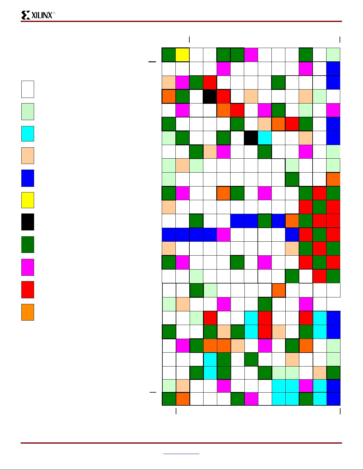
R
Pinout Descriptions
FG676 Footprint -
XC3SD3400A FPGA
Left Half of Package (top
view)
I/O: Unrestricted,
general-purpose user I/O.
314
INPUT: Unrestricted,
general-purpose input pin.
34
DUAL: Configuration,
AWAKE pins, then possible
52
user I/O.
VREF: User I/O or input
voltage reference for bank.
37
CLK: User I/O, input, or
clock buffer input.
32
CONFIG: Dedicated
configuration pins
3
SUSPEND pin.
JTAG: Dedicated JTAG
port pins.
4
GND: Ground
100
VCCO: Output voltage
supply for bank.
40
VCCINT: Internal core
supply voltage (+1.2V).
36
VCCAUX: Auxiliary supply
voltage.
24
Note:
The boxes with
question marks inside
indicate pin differences
from the XC3SD1800A
device. Please see the
"Footprint Migration
Differences" section for
more information.
,
12345678910111213
A
B
L02N_3
INPUT
VREF_3
C
VCCAUX
D
E
L11P_3
F
INPUT ∇GND
G
H
L17N_3
INPUT
J
L24P_3
INPUT
K
L24N_3
L
L29N_3
M
VREF_3
N
L31P_3
Bank 3
L33P_3
P
LHCLK2
L36P_3
R
VREF_3
T
U
L44P_3
V
L47P_3
INPUT
W
L50P_3
Y
L53P_3
A
A
A
L60P_3
B
A
L60N_3
C
A
L65P_3
D
A
INPUT
L66P_3
E
A
F
GND
I/O
∇
∇
I/O
GND
I/O
GND
I/O
I/O
I/O
I/O
GND
I/O
I/O
I/O
GND
I/O
I/O
I/O
GND
PROG_
B
I/O
L02P_3
VCCO_3
∇
GND
∇
VCCO_3
I/O
L11N_3
∇
I/O
L17P_3
INPUT
L20N_3
VREF_3
I/O
L23N_3
VCCO_3
I/O
L29P_3
I/O
L31N_3
I/O
L33N_3
IRDY2
LHCLK3
I/O
L36N_3
VCCO_3
I/O
L44N_3
I/O
L47N_3
INPUT
L50N_3
VREF_3
I/O
L53N_3
I/O
L55P_3
VCCO_3
I/O
L64P_3
I/O
L65N_3
INPUT
L66N_3
VREF_3
VCCAUX
∇
I/O
I/O
L51P_0
L45P_0
I/O
I/O
L51N_0
L45N_0
VCCINT
GND
∇
I/O
TMS
L06P_3
I/O
I/O
L07P_3
L06N_3
I/O
I/O
L14N_3
L07N_3
I/O
I/O
L14P_3
L09N_3
INPUT
VREF_3
GND
∇
INPUT
I/O
L20P_3
L19N_3
I/O
I/O
L23P_3
L22N_3
I/O
I/O
L25N_3
L25P_3
I/O
I/O
L27N_3
L27P_3
I/O
GND
L30N_3
I/O
I/O
L34N_3
L34P_3
LHCLK5
LHCLK4
I/O
I/O
L37P_3
L37N_3
I/O
I/O
L38P_3
L38N_3
INPUT
I/O
L46P_3
L42N_3
INPUT
GND
L46N_3
I/O
I/O
L52P_3
L52N_3
INPUT ∇VCCINT
∇
GND
I/O
L55N_3
∇
VCCAUX
GND
∇
∇
I/O
I/O
L01P_2
L64N_3
M1
I/O
GND
L01N_2
M0
I/O
I/O
L06P_2
L07P_2
I/O
I/O
L06N_2
L07N_2
GND
∇
VCCO_0
I/O
L44P_0
VCCINT
∇
VCCAUX
I/O
L09P_3
GND
∇
VCCO_3
I/O
L19P_3
I/O
L22P_3
VCCAUX
I/O
L28P_3
I/O
L30P_3
VCCO_3
I/O
L40P_3
I/O
L42P_3
I/O
L49P_3
I/O
L49N_3
VCCO_3
I/O
L57P_3
INPUT
VREF_3
∇
VCCAUX
GND
∇
GND
∇
VCCO_2
I/O
L10P_2
GND
I/O
L41P_0
I/O
L41N_0
I/O
L44N_0
VCCINT
∇
GND
I/O
L03P_3
I/O
L10N_3
I/O
L13N_3
I/O
L18P_3
GND
I/O
L28N_3
I/O
L32P_3
LHCLK0
I/O
L39N_3
I/O
L40N_3
GND
I/O
L51N_3
I/O
L59N_3
I/O
L63N_3
I/O
L57N_3
GND
INPUT
VREF_2
I/O
L08P_2
I/O
L08N_2
I/O
L10N_2
GND
VCCO_0
∇
I/O
L42P_0
I/O
L42N_0
INPUT
VREF_0
I/O
L48N_0
I/O
L48P_0
TDI
I/O
L03N_3
I/O
L10P_3
I/O
L13P_3
I/O
L18N_3
I/O
L26N_3
I/O
L32N_3
LHCLK1
I/O
L39P_3
I/O
L45N_3
I/O
L51P_3
I/O
L56P_3
I/O
L59P_3
I/O
L63P_3
I/O
L02P_2
M2
I/O
L02N_2
CSO_B
I/O
L14N_2
GND
∇
I/O
L11P_2
I/O
L11N_2
VCCO_2
∇
I/O
L38P_0
I/O
L38N_0
I/O
L40P_0
I/O
L40N_0
VCCO_0
I/O
L52P_0
VREF_0
I/O
L52N_0
PUDC_B
GND
I/O
L01P_3
I/O
L05N_3
VCCO_3
I/O
L26P_3
GND
I/O
L41P_3
I/O
L45P_3
VCCO_3
I/O
L56N_3
I/O
L61N_3
GND
VCCINT
∇
VCCINT
∇
VCCO_2
I/O
L14P_2
GND
I/O
L18P_2
I/O
L18N_2
I/O
I/O
L36P_0
L33P_0
I/O
I/O
L36N_0
L33N_0
I/O
GND
L34P_0
I/O
I/O
L37N_0
L34N_0
GND
I/O
L37P_0
∇
VCCAUX
VCCINT
∇
∇
I/O
I/O
L47P_0
L46P_0
I/O
I/O
L47N_0
L46N_0
I/O
INPUT
L01N_3
I/O
GND
L05P_3
I/O
I/O
L15N_3
L15P_3
I/O
I/O
L21N_3
L21P_3
I/O
L35P_3
VCCAUX
TRDY2
LHCLK6
I/O
I/O
L35N_3
L41N_3
LHCLK7
I/O
I/O
L43P_3
L43N_3
VREF_3
I/O
I/O
L48N_3
L48P_3
I/O
GND
L61P_3
I/O
VCCAUX
L09P_2
I/O
I/O
L05P_2
L09N_2
I/O
I/O
L05N_2
L12P_2
INPUT
I/O
VREF_2
L12N_2
GND
I/O
L15P_2
I/O
INPUT
L15N_2
VREF_2
INPUT INPUT
I/O
I/O
L19P_2
L22P_2
VS1
I/O
I/O
L19N_2
L22N_2
VS0
GND
VCCO_0
I/O
L32P_0
I/O
L32N_0
VREF_0
INPUT
GND
INPUT
VREF_0
VCCO_0
I/O
L43P_0
I/O
L43N_0
GND VCCINT GND
VCCINT GND VCCINT
GND VCCINT VCCINT
VCCINT GND VCCINT
GND VCCINT GND
VCCINT GND VCCINT
I/O
VCCINT GND
L13N_2
I/O
L13P_2
VCCO_2
VCCINT
∇
GND
VCCAUX
∇
I/O
L23N_2
I/O
L23P_2
VCCO_2
D7
GND
D6
Bank 2
Bank 0
I/O
L29P_0
I/O
L29N_0
I/O
L30N_0
INPUT
I/O
L31P_0
I/O
L31N_0
I/O
L35P_0
I/O
L35N_0
I/O
L39P_0
I/O
L39N_0
I/O
L16P_2
I/O
L16N_2
I/O
L17P_2
RDWR_B
I/O
L17N_2
VS2
I/O
L21P_2
I/O
L21N_2
INPUT
VREF_2
I/O
L24N_2
D4
I/O
L24P_2
D5
INPUT
I/O
L28P_0
GCLK10
I/O
L28N_0
GCLK11
I/O
L30P_0
VCCO_0
I/O
L27P_0
GCLK8
I/O
L27N_0
GCLK9
INPUT
INPUT
VCCAUX
I/O
L20P_2
I/O
L20N_2
I/O
L25N_2
GCLK13
I/O
L25P_2
GCLK12
INPUT
INPUT
GND
I/O
L26N_2
GCLK15
I/O
L26P_2
GCLK14
Figure 18:
FG676 Package Footprint for XC3SD3400A FPGA (top view)
DS610-4 (v2.0) July 16, 2007 www.xilinx.com 93
Product Specification
Page 94

Pinout Descriptions
_
R
14 15 16 17 18 19 20 21 22 23 24 25 26
I/O
I/O
L26N_0
L23N_0
GCLK7
I/O
I/O
L26P_0
L23P_0
GCLK6
I/O
GND
L22N_0
GND
INPUT
VREF_0
∇
I/O
I/O
L20N_0
L24P_0
VREF_0
I/O
I/O
L24N_0
L20P_0
I/O
INPUT
L16P_0
I/O
GND
L16N_0
I/O
INPUT
L25N_0
GCLK5
I/O
VCCINT
L25P_0
GCLK4
VCCINT GND VCCINT
GND
VCCO_0
I/O
L21N_0
I/O
L22P_0
VCCAUX
GND
GND
∇
VCCO_0
I/O
L12P_0
I/O
L12N_0
INPUT
L19N_0
L19P_0
L21P_0
L13N_0
L13P_0
L08N_0
L08P_0
INPUT
VREF_0
L55N_1
GND VCCI NT GND VCCINT
VCCINT GND VCCINT
VCCINT VCCINT GND
VCCINT GND VCCINT
GND VCCI NT GND
I/O
VCCAUX
L35N_2
I/O
I/O
L31P_2
L35P_2
I/O
GND
L31N_2
I/O
I/O
L27P_2
L34N_2
GCLK0
D3
I/O
I/O
L27N_2
L34P_2
GCLK1
INIT_B
I/O
L30N_2
VCCO_2
MOSI
CSI
B
I/O
I/O
L29N_2
L30P_2
I/O
I/O
L32P_2
L29P_2
AWAKE
I/O
I/O
L28N_2
L32N_2
GCLK3
DOUT
I/O
INPUT
L28P_2
VREF_2
GCLK2
I/O
L42N_2
I/O
L42P_2
VCCO_2
INPUT
VREF_2
GND
I/O
L38N_2
I/O
L38P_2
INPUT
VCCO_2
GND
L39N_1
VCCAUX
L27N_1
L17N_1
L46N_2
L46P_2
L43N_2
L43P_2
VCCAUX
INPUT
L33N_2
L33P_2
INPUT
VREF_2
I/O
I/O
I/O
I/O
VCCINT
I/O
VCCINT
I/O
I/O
VCCAUX
GND
I/O
I/O
A15
I/O
A7
I/O
GND
I/O
VCCINT
I/O
VCCINT ∇VCCINT
I/O
I/O
∇
I/O
I/O
I/O
L18N_0
I/O
L18P_0
I/O
L17N_0
I/O
L17P_0
INPUT
∇
∇
INPUT
I/O
L57N_1
I/O
L55P_1
I/O
L47N_1
I/O
L39P_1
A14
I/O
L34P_1
IRDY1
RHCLK6
I/O
L27P_1
A6
I/O
L17P_1
I/O
L12N_1
I/O
L08P_1
∇
I/O
L47N_2
I/O
L47P_2
GND
∇
GND
I/O
L36N_2
D1
I/O
L36P_2
D2
I/O
L15N_0
I/O
L15P_0
GND
GND
∇
VCCO_0
I/O
L02N_0
I/O
L02P_0
VREF_0
GND
I/O
L59P_1
I/O
L57P_1
VCCO_1
I/O
L47P_1
I/O
L34N_1
RHCLK7
GND
I/O
L22P_1
VCCO_1
I/O
L12P_1
I/O
L08N_1
GND
∇
GND
∇
VCCO_2
I/O
L40N_2
I/O
L40P_2
I/O
L37N_2
I/O
L37P_2
I/O
L14N_0
I/O
L14P_0
VREF_0
I/O
L11N_0
I/O
L11P_0
VCCAUX
∇
I/O
L01N_0
I/O
L01P_0
I/O
L64P_1
A24
I/O
L59N_1
I/O
L53N_1
I/O
L53P_1
I/O
L42N_1
A17
I/O
L42P_1
A16
I/O
L30N_1
RHCLK1
I/O
L22N_1
I/O
L14N_1
I/O
L10N_1
SUSPEN
D
I/O
L04P_1
I/O
L01P_1
HDC
INPUT
VREF_2
GND
∇
I/O
L41N_2
I/O
L41P_2
I/O
L39N_2
I/O
L39P_2
GND
I/O
L09N_0
I/O
L09P_0
I/O
L10N_0
I/O
L10P_0
GND
I/O
L64N_1
A25
I/O
L62N_1
A21
I/O
L62P_1
A20
I/O
L50N_1
GND
I/O
L45P_1
I/O
L37N_1
I/O
L30P_1
RHCLK0
I/O
L25P_1
A2
GND
I/O
L14P_1
I/O
L10P_1
I/O
L04N_1
I/O
L01N_1
LDC2
GND
DONE
I/O
L45N_2
I/O
L44N_2
I/O
L44P_2
GND
I/O
L07N_0
VCCO_0
I/O
L05N_0
I/O
L05P_0
VCCAUX
I/O
L58P_1
VREF_1
I/O
L58N_1
VCCO_1
I/O
L49N_1
I/O
L46N_1
I/O
L50P_1
I/O
L45N_1
VCCO_1
I/O
L37P_1
I/O
L25N_1
A3
VCCAUX
I/O
L21N_1
I/O
L18N_1
VCCO_1
I/O
L13P_1
I/O
L09P_1
VCCAUX
I/O
2
I/O
L45P_2
VCCO_2
INPUT
VREF_2
GND
∇
I/O
L07P_0
I/O
L06N_0
I/O
L06P_0
TDO
I/O
L56N_1
I/O
L51P_1
VCCAUX
∇
I/O
L49P_1
I/O
L46P_1
INPUT
L40N_1
I/O
L38N_1
A13
INPUT
L36N_1
I/O
L33P_1
RHCLK4
INPUT
L28P_1
VREF_1
I/O
L26P_1
A4
I/O
L23P_1
I/O
L21P_1
I/O
L18P_1
I/O
L13N_1
I/O
L09N_1
I/O
L07P_1
I/O
L03P_1
A0
GND
∇
I/O
L48N_2
I/O
L48P_2
VCCAUX
TCK GND
∇
GND ∇GND
∇
I/O
GND
L63N_1
A23
I/O
I/O
L61N_1
L61P_1
I/O
VCCO_1
L56P_1
I/O
I/O
L54N_1
L54P_1
INPUT
I/O
VREF_1
L51N_1
∇
VCCO_1
INPUT
∇
∇
I/O
GND
L43N_1
A19
INPUT
I/O
L40P_1
L41P_1
I/O
VCCO_1
L38P_1
A12
INPUT
I/O
L36P_1
L35N_1
VREF_1
A11
I/O
INPUT
L33N_1
L32N_1
RHCLK5
I/O
L31N_1
GND
TRDY1
RHCLK3
I/O
INPUT
L29P_1
L28N_1
A8
I/O
VCCO_1
L26N_1
A5
I/O
GND
L23N_1
∇
VREF_1
I/O
I/O
L19P_1
L19N_1
GND
GND
∇
I/O
I/O
L15P_1
L15N_1
I/O
I/O
L11P_1
L11N_1
I/O
VCCO_1
L07N_1
VREF_1
I/O
I/O
L03N_1
L05N_1
A1
I/O
GND
L02N_1
LDC0
I/O
I/O
L52N_2
L51N_2
CCLK
I/O
I/O
L52P_2
L51P_2
D0
Bank 2
Bank 0
INPUT
VREF_1
∇
I/O
L63P_1
A22
I/O
L60N_1
I/O
L60P_1
GND
VCCAUX
∇
INPUT
VREF_1
∇
I/O
L43P_1
A18
I/O
L41N_1
GND
I/O
L35P_1
A10
INPUT
L32P_1
I/O
L31P_1
RHCLK2
I/O
L29N_1
A9
GND
INPUT
VREF_1
∇
INPUT
VREF_1
∇
VCCAUX
∇
INPUT
∇
GND
I/O
L06N_1
I/O
L06P_1
I/O
L05P_1
I/O
L02P_1
LDC1
GND
Right Half of FG676
A
B
C
D
E
F
G
H
J
K
L
M
N
Bank 1
P
R
T
U
V
W
Y
A
A
A
B
A
C
A
D
A
E
A
F
Package (top view)
94 www.xilinx.com DS610-4 (v2.0) July 16, 2007
Product Specification
Page 95

R
Footprint Migration Differences
Pinout Descriptions
There are multiple migration footprint differences between
the XC3SD1800A and the XC3SD3400A in the FG676
package. These migration footprint differences are shown in
Tab le 6 7 . Migration from the XC3S1400A Spartan-3A
Table 67:
FG676
Ball
G16 IP_0 0 IP_0 0 GND GND G16
G18 N.C. N.C. IP_0 0 VCCINT VCCINT G18
F10 IP_0 0 IP_0 0 VCCINT VCCINT F10
F18 N.C. N.C. IP_0 0 VCCINT VCCINT F18
E20 IP_0 0 IP_0 0 VCCAUX VCCAUX E20
D15 IP_0 0 IP_0 0 GND GND D15
D19 IP_0 0 IP_0 0 GND GND D19
B24 N.C. N.C. IP_0 0 GND GND B24
A23 IP_0 0 IP_0 0 GND GND A23
A24 N.C. N.C. IP_0 0 VCCAUX VCCAUX A24
Y26 IP_L16N_1 1 IP_L16N_1 1 IP_1 1 Y26
W25 IP_L16P_1 1 IP_L16P_1 1 GND GND W25
W26 IP_L20P_1 1 IP_L20P_1 1 VCCAUX VCCAUX W26
V26 IP_L20N_1/
U25 IP_L24P_1 1 IP_L24P_1 1 GND GND U25
U26 IP_L24N_1/
H23 IP_L48P_1 1 IP_L48P_1 1 VCCAUX VCCAUX H23
H24 IP_L48N_1 1 IP_L48N_1 1 IP_1 1 H24
H25 IP_L44N_1 1 IP_L44N_1 1 VCCO_1 1 H25
H26 IP_L44P_1/
G25 IP_L52N_1/
G26 IP_L52P_1 1 IP_L52P_1 1 VCCAUX VCCAUX G26
B25 IP_L65N_1 1 IP_L65N_1 1 GND GND B25
B26 IP_L65P_1/
FG676 Footprint Migration Differences
Spartan-3A Spartan-3A DSP Spartan-3A DSP
XC3S1400A
Typ e
F9 N.C. N.C. IP_0 0 VCCAUX VCCAUX F9
E6 N.C. N.C. IP_0 0 VCCINT VCCINT E6
E9 N.C. N.C. IP_0 0 GND GND E9
D5 N.C. N.C. IP_0 0 VCCINT VCCINT D5
C4 IP_0 0 IP_0 0 VCCINT VCCINT C4
A5 IP_0 0 IP_0 0 GND GND A5
A7 IP_0 0 IP_0 0 VCCO_0 0 A7
VREF_1
VREF_1
VREF_1
VREF_1
VREF_1
XC3S1400A
Bank
1 IP_L20N_1/
1 IP_L24N_1/
1 IP_L44P_1/
1 IP_L52N_1/
1 IP_L65P_1/
XC3SD1800A
Typ e
VREF_1
VREF_1
VREF_1
VREF_1
VREF_1
device in the FG676 package to a Spartan-3A DSP device
in the FG676 package is also possible. The XC3S1800A pin
migration differences have been added to Ta b l e 6 7 for
designs migrating between these devices.
XC3SD1800A
Bank
1 IP_1/VREF_1 1 V26
1 IP_1/VREF_1 1 U26
1 IP_1/VREF_1 1 H26
1 IP_1/VREF_1 1 G25
1 IP_1/VREF_1 1 B26
XC3SD3400A
Typ e
XC3SD3400A
Bank
FG676
Ball
DS610-4 (v2.0) July 16, 2007 www.xilinx.com 95
Product Specification
Page 96

Pinout Descriptions
R
Table 67:
FG676 Footprint Migration Differences
(Continued)
Spartan-3A Spartan-3A DSP Spartan-3A DSP
FG676
Ball
Y8 N.C. N.C. IP_2 2 VCCINT VCCINT Y8
Y11 IP_2 2 IP_2 2 VCCINT VCCINT Y11
Y18 N.C. N.C. IP_2 2 VCCINT VCCINT Y18
Y19 N.C. N.C. IP_2/VREF_2 2 VCCINT VCCINT Y19
W18 N.C. N.C. IP_2 2 VCCINT VCCINT W18
AF2 IP_2 2 IP_2 2 VCCAUX VCCAUX AF2
AF7 IP_2 2 IP_2 2 VCCO_2 2 AF7
AD5 N.C. N.C. IP_2 2 GND GND AD5
AD23 N.C. N.C. IP_2 2 GND GND AD23
AC5 N.C. N.C. IP_2 2 GND GND AC5
AC7 IP_2 2 IP_2 2 GND GND AC7
AC18 IP_2 2 IP_2 2 GND GND AC18
AB10 IP_2/VREF_2 2 IP_2/VREF_2 2 GND GND AB10
AB17 IP_2 2 IP_2 2 VCCAUX VCCAUX AB17
AB20 IP_2 2 IP_2 2 GND GND AB20
AA8 N.C. N.C. IP_2 2 VCCINT VCCINT AA8
AA19 IP_2 2 IP_2 2 GND GND AA19
AC22 N.C. N.C. IO_2 2 IO_2 2 AC22
Y3 IP_L54P_3 3 IP_L54P_3 3 IP_3 3 Y3
Y4 IP_L54N_3 3 IP_L54N_3 3 VCCINT VCCINT Y4
H4 IP_L12N_3/
G1 IP_L16N_3 3 IP_L16N_3 3 IP_3 3 G1
G2 IP_L16P_3 3 IP_L16P_3 3 GND GND G2
G5 IP_L12P_3 3 IP_L12P_3 3 GND GND G5
D1 IP_L08N_3 3 IP_L08N_3 3 VCCAUX VCCAUX D1
D2 IP_L08P_3 3 IP_L08P_3 3 GND GND D2
C1 IP_L04N_3/
C2 IP_L04P_3 3 IP_L04P_3 3 VCCO_3 3 C2
AB3 IP_L62P_3 3 IP_L62P_3 3 GND GND AB3
AB4 IP_L62N_3 3 IP_L62N_3 3 VCCAUX VCCAUX AB4
AA4 IP_L58P_3 3 IP_L58P_3 3 GND GND AA4
AA5 IP_L58N_3/
XC3S1400A
Typ e
VREF_3
VREF_3
VREF_3
XC3S1400A
Bank
3 IP_L12N_3/
3 IP_L04N_3/
3 IP_L58N_3/
XC3SD1800A
Typ e
VREF_3
VREF_3
VREF_3
XC3SD1800A
Bank
3 IP_3/VREF_3 3 H4
3 IP_3/VREF_3 3 C1
3 IP_3/VREF_3 3 AA5
XC3SD3400A
Typ e
XC3SD3400A
Bank
FG676
Ball
Migration Recommendations
There are multiple pinout differences between the
XC3SD1800A and the XC3SD3400A FPGAs in the FG676
package. Please note the differences between the two
devices from Ta bl e 6 7 and take the necessary precautions.
96 www.xilinx.com DS610-4 (v2.0) July 16, 2007
Product Specification
Page 97
R
Pinout Descriptions
Revision History
The following table shows the revision history for this document.
Date Version Revision
04/02/07 1.0 Initial Xilinx release.
05/25/07 1.1 Updates to Tab l e 58 , Table 60, Table 61, Table 62, Table 63, Table 64, Table 65, Table 66. Corrected
06/18/07 1.2 Updated for Production release.
07/16/07 2.0 Added Low-power options.. Added advance thermal data to Table 59.
VREF pins in XC3S1800A FG676 (Table 67). Updated FG676 package footprints for XC3SD1800A
FPGA (Figure 17) and XC3SD3400A FPGA (Figure 18). Minor edits.
SPARTAN-3A DSP
SPARTAN-3A DSP
www.xilinx.com/spartan3adsp
DS610-4 (v2.0) July 16, 2007 www.xilinx.com 97
Product Specification
Page 98

Pinout Descriptions
R
This page intentionally left blank.
98 www.xilinx.com DS610-4 (v2.0) July 16, 2007
Product Specification
 Loading...