

Page 1
0
R
Platform Cable USB
DS300 (v3.2) May 14, 2008
00
Features
Platform Cable USB has these features:
• Supported on Windows and Red Hat Enterprise Linux
• Automatically senses and adapts to target I/O voltage
• Interfaces to devices operating at 5V (TTL), 3.3V
(LVCMOS), 2.5V, 1.8V, and 1.5V
• LED Status Indicator
• CE, USB-IF, and FCC compliant
• Intended for development — not recommended for
production programming
• Pb-free (RoHS-compliant)
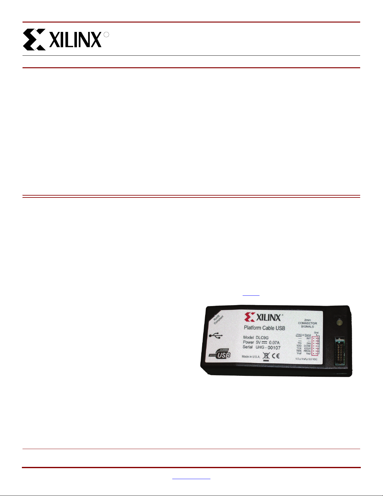
Platform Cable USB Description
Platform Cable USB (Figure 1) is a high-performance
download cable attaching to user hardware for the purpose of
programming or configuring any of the following Xilinx devices:
• ISP Configuration PROMs
• CPLDs
• FPGAs
Platform Cable USB attaches to the USB port on a desktop
or laptop PC with an off-the-shelf Hi-Speed USB A-B cable.
It derives all operating power from the hub port controller.
No external power supply is required. A sustained slaveserial FPGA configuration transfer rate of 24 Mb/s is
possible in a Hi-Speed USB environment. Actual transfer
rates can vary if bandwidth of the hub is being shared with
other USB peripheral devices.
Product Specification
• Configures all Xilinx
♦ All Virtex
♦ All Spartan
♦ XC9500 / XC9500XL / XC9500XV CPLDs
♦ CoolRunner™ XPLA3 / CoolRunner-II CPLDs
♦ XC18V00 ISP PROMs
♦ Platform Flash XCF00S/XCF00P/XL PROMs
♦ XC4000 series FPGAs
®
®
devices
FPGA families
®
FPGA families
• Programs serial peripheral interface (SPI) flash PROMs
the Platform Flash XL configuration and storage device. Target
clock speeds are selectable from 750 kHz to 24 MHz.
Platform Cable USB attaches to target systems using a
14-conductor ribbon cable designed for high-bandwidth data
transfers. An optional adapter that allows attachment of a
flying lead set is included for backward compatibility with
target systems that do not use the ribbon cable connector.
Note:
The next generation, Platform Cable USB II, is now available.
Please refer to the DS593, Platform Cable USB II, for details.
X-Ref Target - Figure 1
Device configuration and programming operations using
Platform Cable USB are supported by iMPACT download
software using Boundary-Scan (IEEE 1149.1 / IEEE 1532),
slave-serial mode, or serial peripheral interface (SPI). Platform
Cable USB supports indirect (via an FPGA IEEE 1149.1
[JTAG] port) programming of select flash memories including
© 2004–2008 Xilinx, Inc. All rights reserved. XILINX, the Xilinx logo, Virtex, Spartan, ISE and other designated brands included herein are trademarks of Xilinx in the United
States and other countries. All other trademarks are the property of their respective owners.
DS300 (v3.2) May 14, 2008 www.xilinx.com
Product Specification 1
Figure 1: Xilinx Platform Cable USB
DS300_01_081006
Page 2
Platform Cable USB
R
Top View
All dimensions are in inches.
Side View
STATU S
1.00
0.65
4.55
2.10
ds300_02_081006
Made in U.S.A.
1 2 3 4 5
Serial UHG -
Model DLC9G
Platform Cable USB
Power 5V 0.07A
2mm
CONNECTOR
SIGNALS
R
Vref
PROG
CCLK
DONE
DIN
INIT
----
or Serial
1.5 < Vref < 5.0 VDC
Vref
TMS
TCK
TDO
TDI
----
JTAG
----
Gnd
HI-SPEED
CERTIFIED
USB
RoHS
Compliant
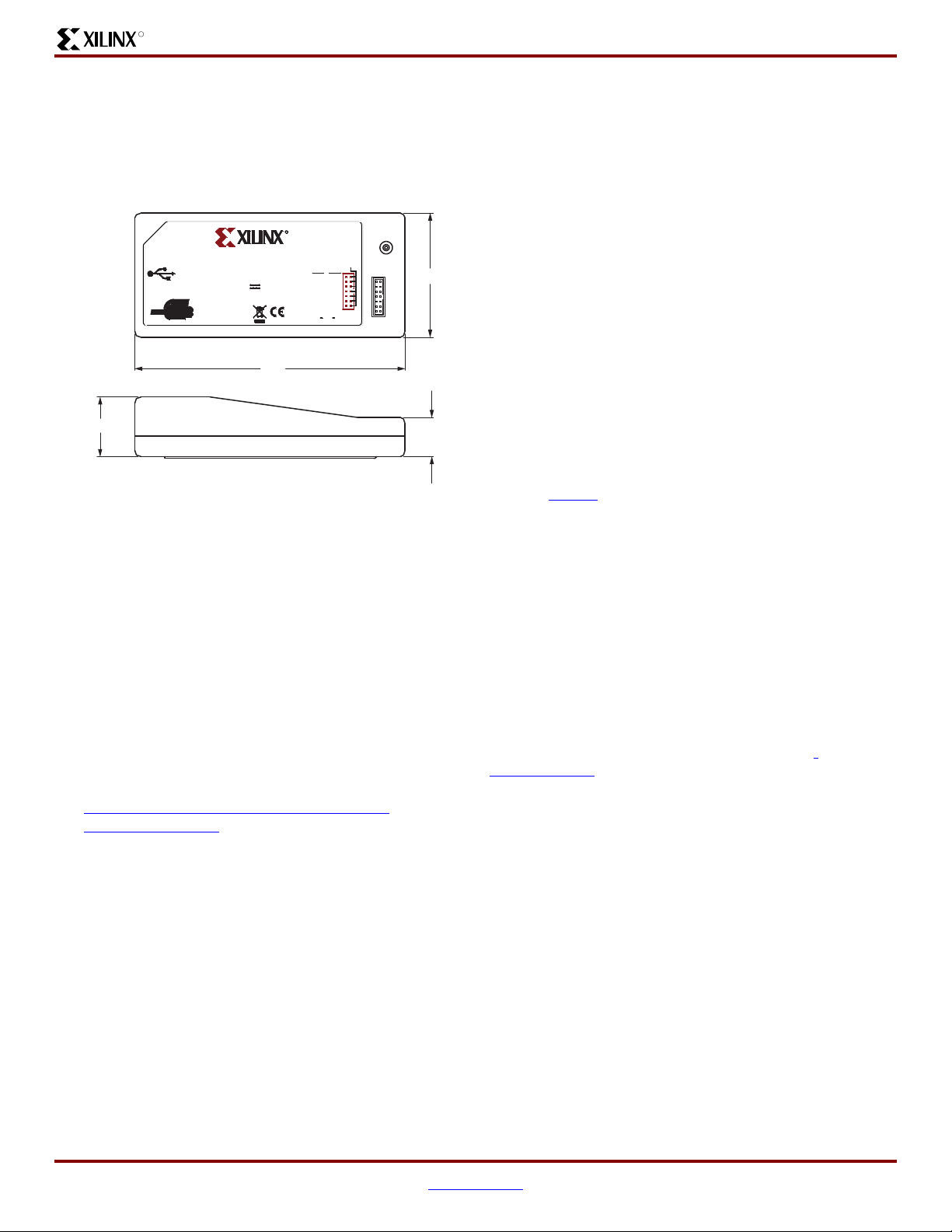
Physical Description
The Platform Cable USB electronics are housed in a
recyclable, fire-retardant plastic case (Figure 2). An internal
EMI shield attenuates internally generated emissions and
protects against susceptibility to radiated emissions.
X-Ref Target - Figure 2
Figure 2: Plastic Case Physical Dimensions
Operation
This section describes how to connect and use Platform
Cable USB.
Minimum Host Computer Requirements
The host computer must contain a USB Host Controller with
one or more USB ports. The controller can reside on the PC
motherboard, or can be added using a PCI expansion card
or PCMCIA card.
Platform Cable USB is supported on systems that meet the
Xilinx ISE
go to:
and select the ISE tool of choice. Platform Cable USB is
designed to take full advantage of the bandwidth of USB 2.0
ports, but it is also backward-compatible with USB 1.1 ports.
Refer to "Hub Types and Cable Performance," page 15 for
additional information on connection environments and
bandwidth.
®
system requirements. For environmental details,
http://www.xilinx.com/products/design_resources/
design_tool/index.htm
hubs, or external self-powered hubs), including legacy USB
1.1 hubs. However, performance is not optimal when
attached to USB 1.1 hubs (refer to "Hot Plug and Play,"
page 5 for an explanation of USB enumeration).
Note:
than 100 mA from the host USB port. The legacy DLC9 cable
model requires 230 mA to operate in USB 2.0 Hi-Speed mode or
150 mA to operate in USB 2.0/1.1 full-speed mode. Some older
root hubs or external bus-powered hubs might restrict devices to
100 mA. The legacy DLC9 cable model does not enumerate on
hubs with the 100 mA restriction.
The DLC9G and legacy DLC9LP cable models draw less
Device Driver Installation
A proprietary device driver is required to use Platform Cable
USB. Xilinx ISE software releases and service packs
incorporate this device driver beginning with version 6.3.03i
for the Windows operating system or 7.1i for the Linux
operating system. Platform Cable USB is not recognized by
the operating system until an appropriate Xilinx ISE,
ChipScope™ Pro or Platform Studio (EDK) software
installation has been completed.
Refer to UG344
, USB Cable Installation Guide, for a
complete guide to installation of the Platform Cable USB
and its device drivers.
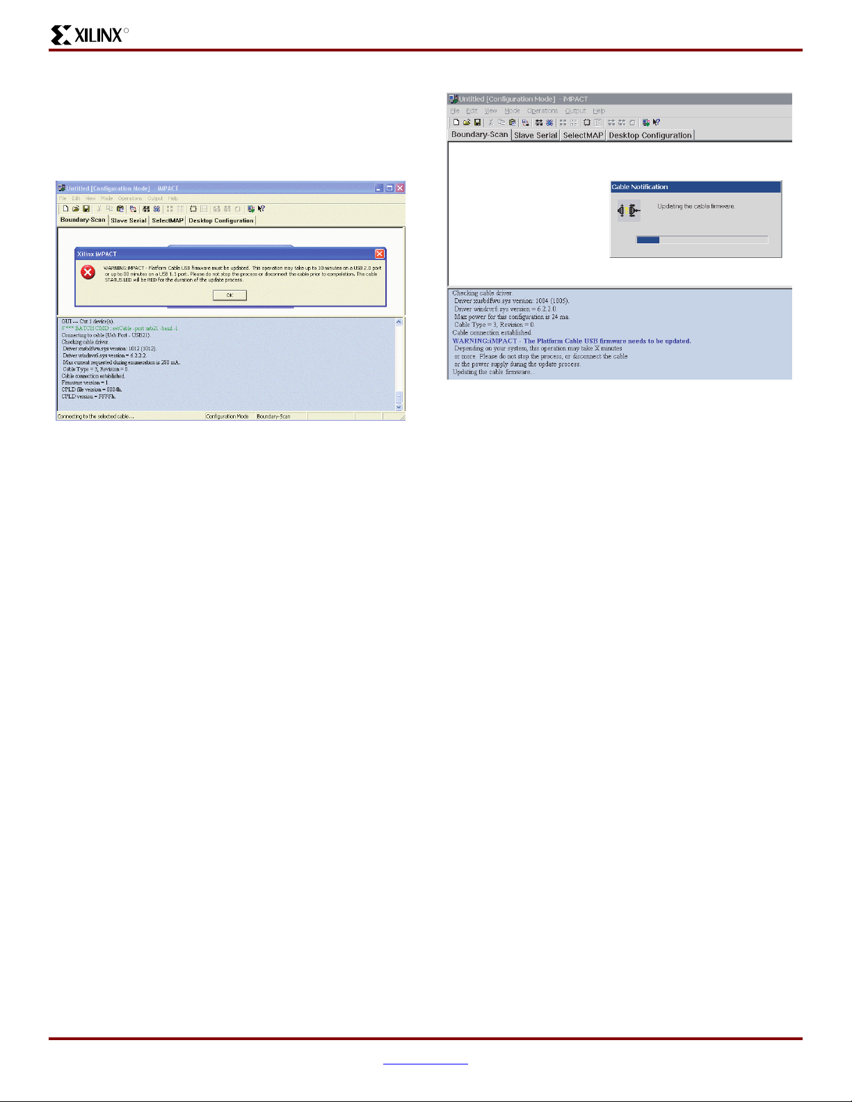
Firmware Updates
Platform Cable USB is a RAM-based product. Application
code is downloaded each time the cable is detected by the
host operating system. USB protocol guarantees that the
code is successfully downloaded.
All files necessary for successful cable communication are
included with every Xilinx ISE software installation CD.
Revised application code is periodically distributed in
subsequent software releases. ISE Service Pack and
WebPACK™ releases can be downloaded from
www.xilinx.com. Project Navigator automatically checks for
new releases when an Internet connection is detected.
When Xilinx applications are invoked and a connection is
established with Platform Cable USB, version information for
several software components is displayed in a command log.
Platform Cable USB also contains an embedded in-circuit
programmable CPLD. Each time a Xilinx application is
invoked, the firmware version for the CPLD is examined.
The CPLD is automatically reprogrammed over the cable if
the firmware version is out of date (see Figure 3).
Although a rare event, when CPLD reprogramming is
necessary, the CPLD reprogramming process can take
considerable time and must not be interrupted once started.
The reprogramming time via a USB 2.0 port can typically
take 10 to 15 minutes. Reprogramming time varies
depending on the ISE software version, the type of USB
port, and the performance of the host system. Later
versions of the ISE software can reprogram CPLDs faster
than older versions.
Operating Power
Platform Cable USB is a bus-powered device that draws
less than 100 mA from the host USB port under all
operating conditions, automatically adapting to the
capabilities of the host USB port to achieve the highest
possible performance.
Platform Cable USB enumerates on any USB port type (for
example, USB ports on root hubs, external bus-powered
DS300 (v3.2) May 14, 2008 www.xilinx.com
Product Specification 2
Page 3
Platform Cable USB
R
DS300_03_112504
DS300_04_110604
During a CPLD update, the Status LED illuminates red, and
a progress bar indicates communication activity (see
Figure 4). CPLD updates should never be interrupted. When
an update is complete, the Status LED returns to either
amber or green, and the cable is ready for normal operation.
X-Ref Target - Figure 3
Figure 3: CPLD Update Notification
X-Ref Target - Figure 4
Figure 4: CPLD Update Progress Bar
DS300 (v3.2) May 14, 2008 www.xilinx.com
Product Specification 3
Page 4
Platform Cable USB
R
ds300_05_112904
ds300_06_112904
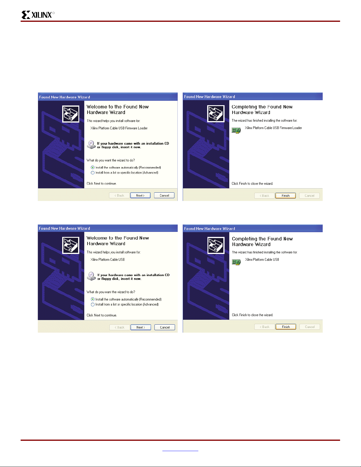
Found New Hardware Wizard (for Windows Only)
Platform Cable USB should be disconnected from the host system during the initial software installation. The first time a
cable is attached after software installation, Windows invokes the Found New Hardware wizard and registers device drivers
for the Platform Cable USB Firmware Loader (see Figure 5) and for the Platform Cable USB itself (see Figure 6).
Windows invokes the Found New Hardware flow each time Platform Cable USB is plugged into a different physical USB port
for the first time. The wizard screens could be slightly different for Windows 2000 environments.
X-Ref Target - Figure 5
X-Ref Target - Figure 6
Figure 5: a) Firmware Loader PID Detected; b) Firmware Loader Driver Registered
Figure 6: a) Application PID Detected; b) Application Driver Registered
DS300 (v3.2) May 14, 2008 www.xilinx.com
Product Specification 4
Page 5
Platform Cable USB
R
DS300_07_110604
DS300_08_110604
DS300_09_110604
Hot Plug and Play
The cable can be attached and removed from the host
computer without the need to power-down or reboot. There
is a momentary delay after connecting the cable to an
available port before the Status LED illuminates. This
process is called enumeration.
When Platform Cable USB completes the enumeration
process on a Windows system, a "Programming cables" entry
appears in the Windows Device Manager (see Figure 7). To
display Device Manager, right-click on My Computer, then
select Properties → Hardware → Device Manager.
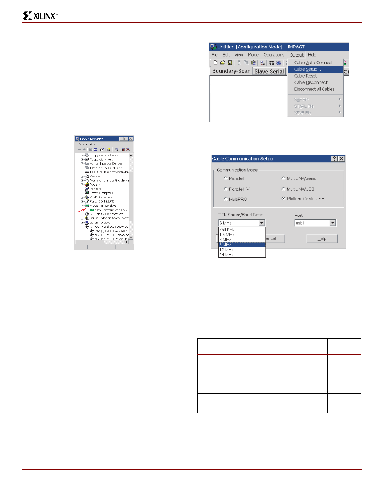
X-Ref Target - Figure 7
X-Ref Target - Figure 8
Figure 8: iMPACT Cable Selection Drop-Down Menu
X-Ref Target - Figure 9
Figure 7: Device Manager Cable Identification
iMPACT Configuration Cable Selection
Platform Cable USB can be designated as the "active"
configuration cable by following the auto-connect sequence
for configuring devices that is displayed when first starting
an iMPACT session.
Note:
as the "active" cable if both PC4 and Platform Cable USB are
connected simultaneously.
Alternatively, the cable can be manually selected using
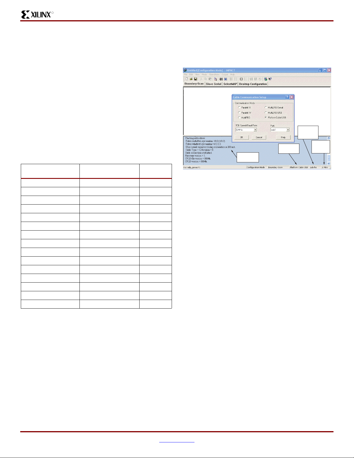
the Output → Cable Setup option on the iMPACT toolbar
(see Figure 8).
When the Cable Communications Setup dialog box is
displayed (Figure 9), the Communication Mode radio
button must be set to "Platform Cable USB."
Before switching from the Boundary-Scan mode to the Slave
Serial mode or vice versa, use Output → Cable Disconnect.
After the mode switch is complete, reestablish the cable
connection using the Output → Cable Setup dialog.
If an iMPACT session is active when the cable is removed,
the Status bar immediately indicates "No Connection."
During the auto-connect sequence, iMPACT selects PC4
Figure 9: iMPACT Cable Communication Setup Dialog
Configuration Clock Speed
The Platform Cable USB configuration clock
(TCK_CCLK_SCK) frequency is selectable. Ta bl e 1 shows
the complete set of available TCK_CCLK_SCK speed
selections for high-power USB ports.
Tab l e 1 : Speed Selection for High-Power Ports
Selection
124MHz
212MHz
3 (default) 6 MHz
43MHz
51.5MHz
6 750 kHz
In slave-serial or SPI mode, the TCK_CCLK_SCK speed
can be set to any one of the available selections. By default,
the TCK_CCLK_SCK speed is set to 6 MHz. Users should
take care to select a TCK_CCLK_SCK frequency that
matches the slave-serial clock (CCLK or SPI clock)
specification of the target device.
TCK_CCLK_SCK
Frequency
Units
DS300 (v3.2) May 14, 2008 www.xilinx.com
Product Specification 5
Page 6
Platform Cable USB
R
DS300_10_111904
Active Cable
Identification
Full-Speed or
High-Speed
Connection
Active
TCK_CCLK
Frequency
Command Log
Text Display
In Boundary-Scan mode, iMPACT 7.1i (and later) queries
the BSDL file of each device in a target Boundary-Scan
chain to determine the maximum Boundary-Scan clock
(JTAG TCK) frequency. iMPACT 7.1i (and later)
automatically restricts the available TCK_CCLK_SCK
selections to frequencies that are less than or equal to the
CPLD version = 0004h
Cable Connection Established
Note: The actual revision number can be expected to change
with new software releases.
X-Ref Target - Figure 10
slowest device in the chain. By default, iMPACT 7.1i (or
later) selects either 6 MHz or the highest common
frequency when any device in the Boundary-Scan chain is
not capable of 6 MHz operation. Tab l e 2 shows the
maximum supported JTAG TCK frequency for a variety of
Xilinx devices. See the device data sheet or BSDL file for
maximum JTAG TCK specifications.
Note:
TCK_CCLK_SCK selections in Boundary-Scan mode.
Accordingly, users should take care to select a TCK_CCLK_SCK
frequency that matches the JTAG TCK specifications for the
slowest device in the target Boundary-Scan chain.
iMPACT versions earlier than 7.1i do not restrict the
Tab l e 2 : Maximum JTAG Clock Frequencies
Device Family
XC9500/XL/XV 10 MHz
XPLA3 10 MHz
CoolRunner-II 33 MHz
XC18V00 10 MHz
XCF00S/XCF00P 15 MHz
Virtex 33 MHz
Virtex-II 33 MHz
Virtex-II Pro 33 MHz
Virtex-4 33 MHz
Virtex-5 33 MHz
Spartan 5 MHz
Spartan-II 33 MHz
Spartan-3 33 MHz
Spartan-3A 10 MHz
Spartan-3E 10 MHz
Maximum JTAG Clock
Frequency
Units
Figure 10: iMPACT Status Bar
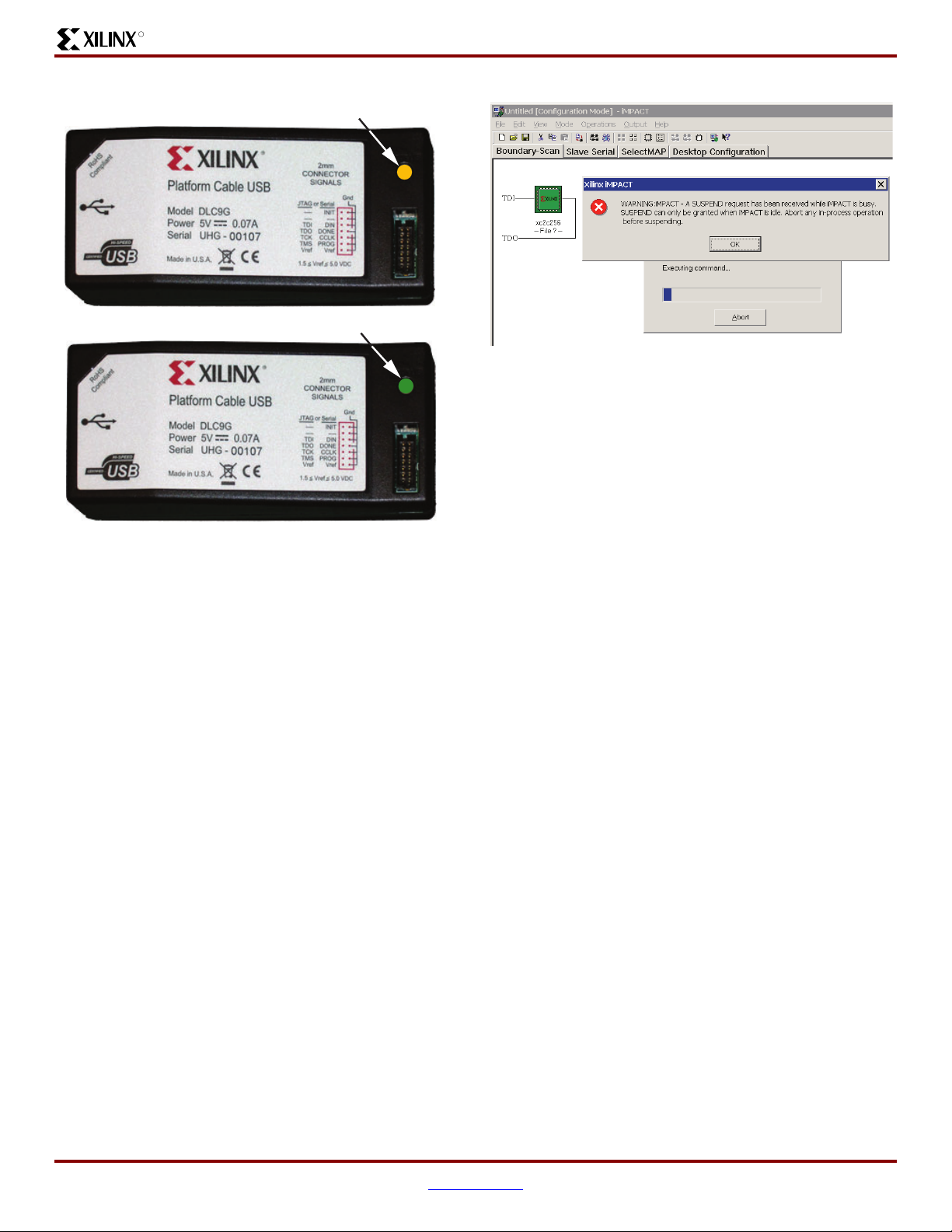
Status Indicator
Platform Cable USB uses a bi-color Status LED to indicate
the presence of target voltage. When the ribbon cable is
connected to a mating connector on the target system, the
Status LED is illuminated as a function of the voltage
present on pin 2 (V
Users must design their system hardware with pin 2
attached to a voltage plane that supplies the JTAG, SPI, or
slave-serial pins on the target device(s). Some devices have
separate power pins for this purpose (VAUX), while others
have a common supply for both VCCIO and the JTAG pins
(TCK, TMS, TDI, and TDO). Refer to the target device Data
Sheet for details on slave-serial or JTAG pins.
The Status LED is amber (see Figure 11) when any one or
more of the following conditions exist:
REF
).
• The ribbon cable is not connected to a target system
A Status bar on the bottom edge of the iMPACT GUI
provides useful information about operating conditions. If
the host port is USB 1.1, Platform Cable USB connects at
full-speed, and the Status bar shows "usb-fs." If the host
port is USB 2.0, Platform Cable USB connects at Hi-Speed
• The target system is not powered
• The voltage on the V
pin is < +1.5V
REF
The Status LED is green when all of the following
conditions exist:
and the Status bar shows "usb-hs."
• The ribbon cable is connected to a target system
The active TCK_CCLK_SCK frequency is shown in the
lower right-hand corner of the Status bar (see Figure 10).
The command log also includes information about
communication with the cable. When the cable is selected
using the Cable Communication Setup dialog box, the
• The target system is powered
• The voltage on the V
pin is ≥ +1.5V
REF
The Status LED is Off whenever Platform Cable USB enters a
Suspend state, or is disconnected from a powered USB port.
command log indicates:
Firmware version = 1
CPLD file version = 0004h
DS300 (v3.2) May 14, 2008 www.xilinx.com
Product Specification 6
Page 7
Platform Cable USB
R
ds300_11a_113004
X-Ref Target - Figure 11
Amber indicates no target voltage
Green indicates target voltage present
Figure 11: Status LEDs Indicating Target Voltage
Suspend State
DS300_11_081006
X-Ref Target - Figure 12
Figure 12: Suspend Warning When iMPACT Is Busy
The target interface logic, including drivers for
TCK_CCLK_SCK, TMS_PROG_SS, and TDI_DIN_MOSI,
is not powered in the Suspend mode. These signals float
to any DC bias level provided by the target hardware
during Suspend.
Note:
in Suspend mode. This is equivalent to a physical disconnect of
the cable. When operation resumes, it is necessary to manually reestablish a connection to the cable using the Output → Cable
Setup toolbar selection.
Some computers remove power entirely from the USB port
Every USB device, including Platform Cable USB, can be
placed into a Suspend state by the host operating system.
This can occur during any of the following usage scenarios:
• The Suspend function key on a laptop computer is
pressed.
• The display panel of a laptop is placed in the closed
position for transport while applications are running.
• There is an extended period of time without data
transfer activity on the cable when connected to a
battery-powered laptop.
• There is an extended period of time without data transfer
activity on the cable when connected to a desktop PC
configured with an "Energy Efficiency" option.
The purpose of the Suspend state is to reduce overall
power consumption. Suspend requests can be either global
or port-specific.
Platform Cable USB must consume less than 500 µA from
the hub port when it enters the Suspend state.
Consequently, the Status LED is turned off and remains off
until commanded to resume.
If an iMPACT operation is in progress when Suspend is
attempted, iMPACT displays a message indicating that
Suspend is blocked until the operation is complete or is
prematurely terminated (Figure 12).
Platform Cable USB Connections
This section of the data sheet discusses physical
connections from Platform Cable USB to the host PC and
the target system.
High-Performance Ribbon Cable
A 6" ribbon cable is supplied and recommended for
connection to target systems (refer to Figure 13). The cable
incorporates multiple signal-ground pairs and facilitates
error-free connections.
To take advantage of the ribbon cable, a mating connector
must be incorporated into the target system. This connector
is normally installed only during prototype checkout. When
the production hardware is functional and the ISP devices
can be configured from alternate sources, the connector can
be eliminated as a cost reduction option. Maintaining the
footprint for this connector is a wise choice if space permits.
The connector is a 2 mm shrouded keyed header. See
"Target Interface Connectors," page 8 for vendor part
numbers and pin assignments.
DS300 (v3.2) May 14, 2008 www.xilinx.com
Product Specification 7
Page 8

Platform Cable USB
R
DS300_12_090506
DS300_14_113004
ds300_15_110804
X-Ref Target - Figure 13
Figure 13: High-Performance Ribbon Cable
Notes:
1. Ribbon Cable: 14 conductor, 1.0 mm center, round conductor flat
cable, 28 AWG (7 x 36) stranded conductors, gray PVC with pin 1
edge marked.
2. 2 mm ribbon female polarized connector, IDC connection to
ribbon. Contacts are beryllium copper plated, 30 micro-inches
gold plating over 50 micro-inches nickel. The connectors mate to
0.5 mm square posts on 2 mm centers.
3. One ribbon cable is supplied with the Platform Cable USB.
Additional ribbon cables can be purchased separately (see
"Ordering Information," page 19).
Notes:
1. This method of connection is not recommended because it can
result in poor signal integrity. Additionally, damage can result if
the leads are unintentionally connected to high voltages.
2. One flying wire adapter with wires is supplied with the Platform
Cable USB. Additional flying wire adapters with wires can be
purchased separately (see "Ordering Information," page 19).
Physical Connection to the Host
Each Platform Cable USB includes a detachable, Hi-Speed
certified 1.8 meter A-B cable (Figure 16). Under no
circumstances should user-supplied cables exceed 5 meters.
Sub-channel cables (intended for low-speed 1.5 Mb/s
signaling) should not be used with Platform Cable USB.
A standard series B receptacle is incorporated into the left
side of the case for mating with the detachable Hi-Speed A-B
cable. A separate chassis ground is attached to the A-B cable
drain wire and returns ESD current to the host system ground.
X-Ref Target - Figure 16
Flying Wire Adapter
An adapter is provided for attachment to legacy target
systems that do not incorporate a shrouded male 2 mm
connector (Figure 14). The adapter makes it possible to use
flying wires for connection to distributed terminals on a
target system.
The adapter is a small circuit board with two connectors
(Figure 15). The connector on the bottom side of the
adapter mates with the 14-pin Platform Cable USB male
2 mm connector. A 7-pin right-angle header on the top
side of the adapter mates with the standard Xilinx flying
wire set (included).
X-Ref Target - Figure 14
RoHS
Compliant
HI-SPEED
CERTIFIED
USB
R
Platform Cable USB
Model DLC9G
Power 5V 0.07A
Serial UHG -
1 2 3 4 5
Made in U.S.A.
Figure 14: Flying Wire Adapter (Top) with Wires
X-Ref Target - Figure 15
2mm
CONNECTOR
SIGNALS
JTAG
orSerial
----
INIT
----
----
TDI
DIN
DONE
TDO
TCK
CCLK
TMS
PROG
Vref
Vref
1.5 < Vref < 5.0 VDC
STATU S
Gnd
R
JTAG | SERIAL Vref | Vref
ADAPTER
GND | GND
TCK | CCLK
--- | INIT
TDO | DONE
TDI | DIN
TMS | PROG
DS300_13_081006
Figure 16: Standard A-B Host Interface
Cable and Series B Receptacle
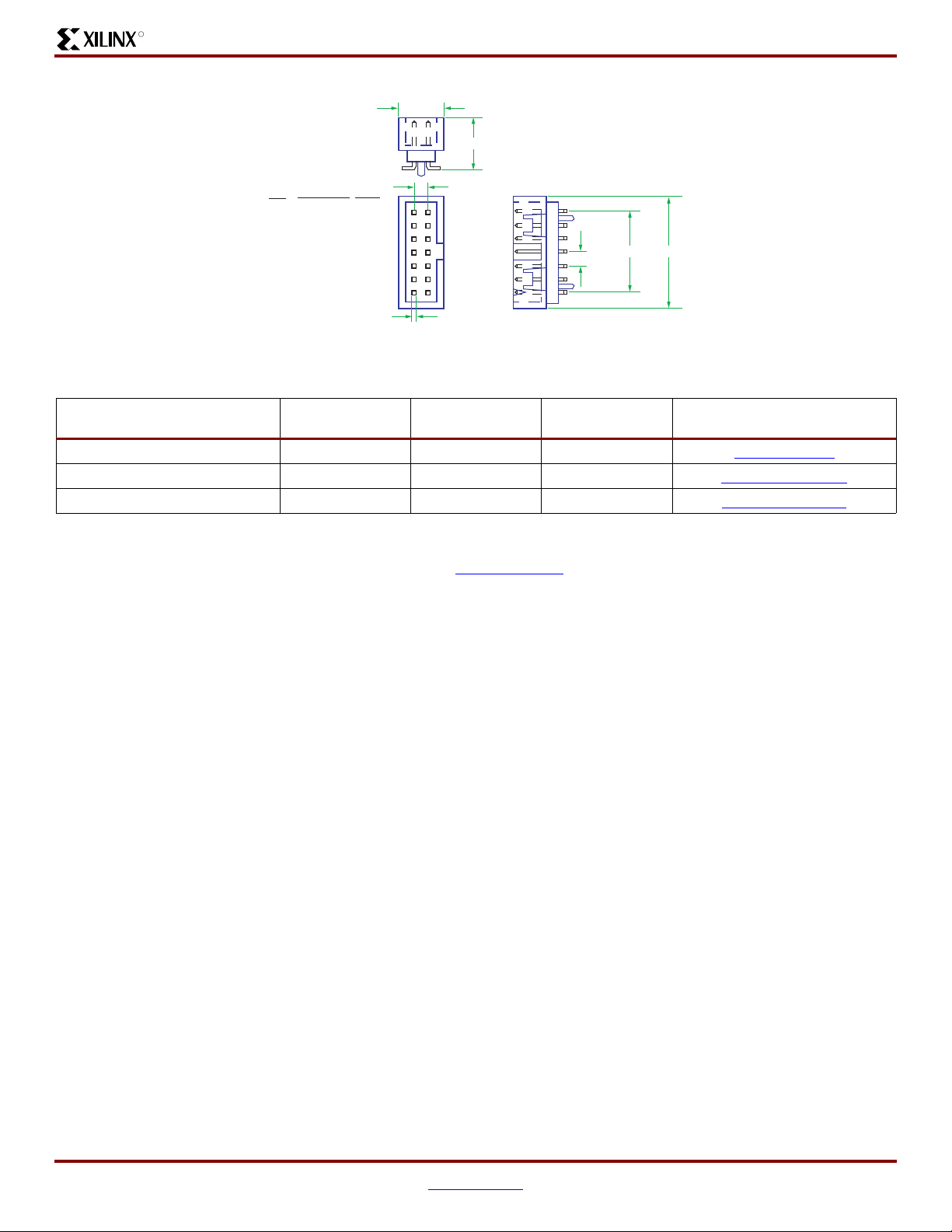
Target Interface Connectors
Mating connectors for attachment of the high-performance
ribbon cable to a target system are available in both
through-hole and surface mount configurations (Figure 17).
Shrouded and/or keyed versions should always be used to
guarantee proper orientation when inserting the cable. The
connector requires only 0.162 in
The target system voltage applied to pin 2 of this connector
is used as a reference for the output buffers that drive the
TDI_DIN_MOSI, TCK_CCLK_SCK, and TMS_PROG_SS
pins.Ta bl e 3 provides some third-party sources for mating
connectors that are compatible with the Platform Cable
USB ribbon cable.
2
of board space.
Figure 15: Flying Wire Adapter (Side) w/o Wires
DS300 (v3.2) May 14, 2008 www.xilinx.com
Product Specification 8
Page 9
R
X-Ref Target - Figure 17
Platform Cable USB
0.248"
0.299"
SPI
NC
NC
MOSI
MISO
SCK
SS
V
REF
JTAGSlave Serial
NCINIT 14
NCNC 12
TDIDIN 10
TDODONE
8
TCKCCLK
6
TMSPROG
4
V
V
REF
REF
2
0.0787" (2 mm)
GND
13
11
GND
9
GND
7
GND
5
GND
3
GND
(1)
1
GND
0.020" (0.5 mm) SQ. TYP.
0.0787"
TYP.
0.656"
0.472"
DS300_16_021507
Figure 17: Target Interface Connector Dimensions and Signal Assignments
Tab l e 3 : Mating Connectors for 2 mm Pitch, 14-Conductor Ribbon Cable
Manufacturer
(1)
SMT,
Vertical
Molex 87832-1420 87831-1420 87833-1420 www.molex.com
FCI 98424-G52-14 98414-G06-14 98464-G61-14 www.fciconnect.com
Comm Con Connectors 2475-14G2 2422-14G2 2401R-G2-14 www.commcon.com
Notes:
1. Some manufacturer pin assignments do not conform to Xilinx pin assignments. Please refer to the manufacturer’s data sheet for more information.
2. Additional ribbon cables can be purchased separately from the Xilinx Online Store
Through-Hole,
Vertical
Through-Hole,
Right Angle
.
Web Site
DS300 (v3.2) May 14, 2008 www.xilinx.com
Product Specification 9
Page 10

R
TDI_DIN_MOSI and TMS_PROG_SS Timing Specifications
DS300_17_021707
TDI_DIN_MOSI Changes
on Negative Edge of
TCK_CCLK_SCK (G2)
TMS_PROG_SS Changes on Negative
Edge of TCK_CCLK_SCK (G1)
Platform Cable USB
For JTAG, SPI, and slave-serial configuration modes, the
TDI_DIN_MOSI and TMS_PROG_SS outputs change on
falling edges of TCK_CCLK_SCK (Figure 18). Target
devices sample TDI_DIN_MOSI and TMS_PROG_SS on
rising edges of TCK_CCLK_SCK. The minimum setup time
T
TTSU(MIN)
for target device sampling of TDI_DIN_MOSI or
TMS_PROG_SS is:
T
TTSU(MIN)
=T
CLK/2
– T
CPD(MAX)
= 20.83 ns – 9.2 ns
= 11.63 ns
X-Ref Target - Figure 18
where T
and T
CPD(MAX)
is the TCK_CCLK_SCK Low time at 24 MHz,
CLK/2
is the maximum TDI_DIN_MOSI or
TMS_PROG_SS propagation delay relative to
TCK_CCLK_SCK inherent in the output stage of the cable.
Reducing the TCK_CCLK_SCK frequency increases the
data setup time at the target.
Note:
at 24 MHz might not be possible when using a VREF below 3.3V
due to the increased propagation delay through the output buffer
stage of the cable.
Timing specifications apply when VREF = 3.3V. Operation
Figure 18: TDI_DIN_MOSI and TMS_PROG_SS Timing with Respect to TCK_CCLK_SCK
TDO/MISO Timing Issues
When read operations are being performed in Boundary-Scan
or SPI mode, there must be sufficient time during each onehalf clock cycle for TDO/MISO to propagate back to the cable
for sampling. Figure 19, Figure 20, page 11, and Figure 21,
page 11 illustrate a potential problem when a 24 MHz
TCK_CCLK_SCK frequency is selected. An output buffer in
Platform Cable USB introduces a phase delay of 4 ns between
the cable and the target. (See cursors C1 and C2 in Figure 19,
page 11 for the CBL_TCK to TCK_CCLK_SCK delay.)
The target device has a variable propagation delay from the
negative edge of TCK_CCLK_SCK to assertion of
TDO_DONE_MISO. (Refer to Figure 20 for the
TCK_CCLK_SCK to TDO_DONE_MISO delay.) For
DS300 (v3.2) May 14, 2008 www.xilinx.com
Product Specification 10
example, Figure 20 shows a 12 ns TDO delay for an
XC2C256-VQ100 CPLD.
Finally, signal conditioning circuitry in Platform Cable USB
introduces a third phase delay of approximately 12 ns between
TDO_DONE_MISO and the logic that samples the signal.
Note:
CBL_TDO delay.)
(Refer to Figure 21, page 11 for the TDO_DONE_MISO to
Data is sampled approximately 11 ns after the rising edge of
CBL_TCK. The total propagation delay must be carefully
considered to successfully operate at 24 MHz. Refer to
Figure 30, page 18 for set-up timing requirements.
Page 11

Platform Cable USB
R
DS300_18_110204
DS300_19_110204
DS300_20_110204
X-Ref Target - Figure 19
Figure 19: TDO_DONE_MISO Timing with Respect to TCK_CCLK_SCK (CBL_TCK to TCK_CCLK_SCK Delay)
X-Ref Target - Figure 20
Figure 20: TDO_DONE_MISO Timing with Respect to TCK_CCLK_SCK (TCK_CCLK_SCK to TDO_DONE_MISO Delay)
X-Ref Target - Figure 21
Figure 21: TDO_DONE_MISO Timing with Respect to TCK_CCLK_SCK (TDO_DONE_MISO to CBL_TDO Delay)
DS300 (v3.2) May 14, 2008 www.xilinx.com
Product Specification 11
Page 12

Platform Cable USB
R
I/O
XFCE PIN
V
CC33_SW
CPLD
2 mm Connector
Internal
Three-State
Control
High-Z
V
REF_A
V
REF_A
NC7SZ125
DS300_22_120904
DS300_22_113004
I/O
XFCE PIN
CPLD
2 mm Connector
V
REF_A
V
CC33
BAT54
LT1719
DS300_23_120904
Target Reference Voltage Sensing (V
REF
Platform Cable USB incorporates an over-voltage clamp on
the V
clamped voltage (V
pin of the 2 mm ribbon cable connector. The
REF
) supplies a high-slew-rate buffer
REF_A
(NC7SZ125) that drives each of the three output signals.
V
must be a regulated voltage.
REF
Note:
Do not insert a current-limiting resistor in the target system
between the VREF supply and pin 2 on the 2 mm connector.
No damage to Platform Cable USB occurs if the A-B cable
is unplugged from the host while the ribbon cable or flying
leads are attached to a powered target system. Similarly, no
damage to target systems occurs if Platform Cable USB is
powered and attached to the target system while the target
system power is off.
Buffers for the output signals (TCK_CCLK_SCK,
TMS_PROG_SS, and TDI_DIN_MOSI) are set to high-Z
when V
linearly tracks voltage changes on the V
1.40V ≤ V
approximately 3.30V when 3.30 ≤ V
Refer to Ta bl e 4 for the relationship between V
drops below 1.40V. The output buffer amplitude
REF
≤ 3.30V. Amplitude is clamped at
REF
REF
pin when
REF
≤ 5.00V.
REF
voltage
and output signal amplitude.
a defined logic level when the buffers are set to high-Z. The
)
pull-up resistors terminate to V
X-Ref Target - Figure 22
REF_A
.
Figure 22: Target Interface Driver Topology
Refer to Figure 23 to determine the expected value of
V
X-Ref Target - Figure 23
as a function of V
REF_A
REF
.
Tab l e 4 : Output Signal Level as a Function of the V
V
Voltage on Target
REF
System (VDC)
0.00 ≤ V
1.40 ≤ V
3.30 ≤ V
< 1.40 High-Z Amber
REF
< 3.30 V
REF
≤ 5.00 ≅ 3.3 Green
REF
Output Signal
Levels (VDC)
REF
Status LED
Color
Green
Notes:
1. There are weak pull-up resistors to VREF_A on each of the three
output drivers (TCK_CCLK_SCK, TMS_PROG_SS, and
TDI_DIN_MOSI). The output drivers are active only during
configuration and programming operations. Between operations,
the drivers are set to high-Z.
Xilinx applications actively drive the outputs to logic 1 before
setting the respective buffer to high-Z, avoiding the
possibility of a slow rise-time transition caused by a charge
path through the pull-up resistor into parasitic capacitance
on the target system.
Output Driver Structure
Platform Cable USB drives three target signals:
TCK_CCLK_SCK, TMS_PROG_SS, and TDI_DIN_MOSI.
Each of these signals incorporates the same driver
topology. A Xilinx XC2C256 Coolrunner-II CPLD generates
the output signals.
REF
Figure 23: V
as a Function of V
REF_A
REF
Input Receiver Structure
A Schottky diode is used to protect the TDO_DONE_MISO
voltage comparator (Figure 24). In effect, Platform Cable
USB looks for voltages below V
tolerates voltages much higher than V
could be terminated to a supply other than V
X-Ref Target - Figure 24
MAX to detect logic 0, and
IL
because TDO
REF_A
REF
.
Each signal is routed to an external NC7SZ125 high-speed
CMOS buffer (Figure 22). Series-damping resistors (30Ω)
reduce reflections. Weak pull-up resistors (20 kΩ) maintain
DS300 (v3.2) May 14, 2008 www.xilinx.com
Product Specification 12
Figure 24: Target Interface Receiver Topology
Page 13

Platform Cable USB
R
SN65LVDS105
Four Differential
Drivers
SN65LVDS2 (2)
TCK_CCLK
TCK_CCLK_1
1
4
TCK_CCLK_4
DS300_24_110804
Locate driver package adjacent to 2mm connector
Route A & B traces for each differential
pair in parallel with equal length and
consistent spacing
Series Termination Resistor
Locate one receiver adacent
to each target device
Four
Buffered
Clocks
Signal Integrity
Platform Cable USB uses high-slew-rate buffers to drive
TCK_CCLK_SCK, TMS_PROG_SS, and TDI_DIN_MOSI.
Each buffer has a 30Ω series termination resistor. Users
should pay close attention to PCB layout to avoid
transmission line effects. Visit the Xilinx Signal Integrity
Central website, and see specifically Xilinx Application Note
XAPP361, Planning for High Speed XC9500XV Designs, for
detailed signal integrity assistance.
If the target system has only one programmable device, the
2 mm connector should be located as close as possible to
the target device. If there are multiple devices in a single
chain on the target system, users should consider buffering
TCK_CCLK_SCK. Differential driver/receiver pairs provide
excellent signal quality when the rules identified in
Figure 25 are followed. Buffering is essential if target
devices are distributed over a large PCB area.
Each differential driver and/or receiver pair contributes
approximately 5 ns of propagation delay. This is
insignificant when using 12 MHz or slower clock speeds.
Each differential receiver can drive multiple target devices if
there are no branches on the PCB trace and the total trace
length is less than four inches. A series termination resistor
should be placed adjacent to the single-ended output of the
differential receiver.
X-Ref Target - Figure 25
Figure 25: Differential Clock Buffer Example
Note:
TCK_CCLK_SCK and the 24 MHz clock rate is used, it is
recommended that the same buffer type also be provided for
TMS_PROG_SS. This maintains a consistent phase relationship
between TCK_CCLK_SCK and TMS_PROG_SS. A buffer is not
needed for TDI_DIN_MOSI, because it sees only one load.
If the target system incorporates a buffer for
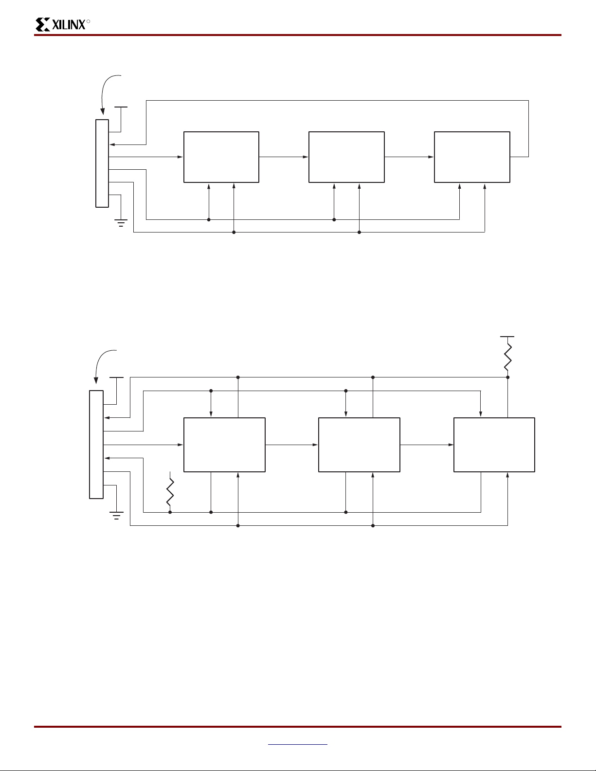
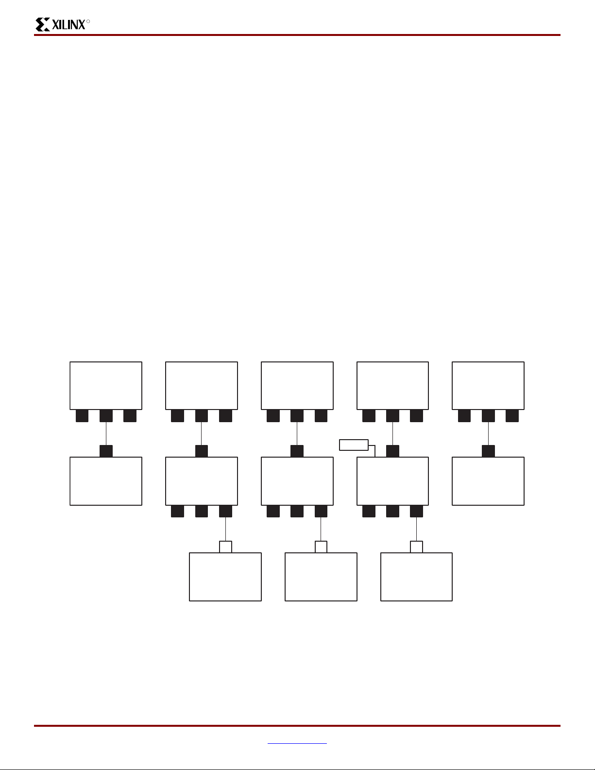
Target System Connections
Multiple devices can be cascaded when using either JTAG
or slave-serial topology in target systems. Figure 27,
page 14 shows typical JTAG connections, and Figure 28,
page 14 shows an example of slave-serial routing.
The Platform Cable USB can connect directly to a single
SPI flash device. Figure 26 shows example SPI flash
connections. Refer to XAPP951
with SPI Serial Flash, for a detailed reference design
showing the cable connections for programming an FPGA
bitstream into a SPI flash device.
The DONE pin on FPGAs can be programmed to be an
open-drain or active driver. For cascaded slave-serial
topologies, an external pull-up resistor should be used, and
all devices should be programmed for open-drain operation.
If the 2 mm connector is located a significant distance from
the target device, it is best to buffer TCK_CCLK_SCK, at a
minimum. These diagrams are intended to represent the
logical relationship between Platform Cable USB and target
devices. Refer to "Signal Integrity," page 13 for additional
buffering and termination information.
, Configuring Xilinx FPGAs
X-Ref Target - Figure 26
+3.3V
2 mm
Connector
V
2
REF
MISOD8
MOSIQ10
SSS4
SCK C6
(2)
GND
Notes:
1. The example shows pin names for an STMicrosystems M25Pxx serial flash
2. Attach the following 2 mm connector pins to digital ground: 1, 3, 5, 7, 9, 11, 13.
3. Typically, an FPGA and other s
X
device. SPI flash devices from other vendors can have different pin names and
requirements. See the SPI flash data sheet for the equivalent pins and device
requirements.
connected to the SPI bus. The other devices on the SPI bus must be disabled
when the cable is connected to the 2 mm connector to avoid signal contention.
When a Xilinx FPGA is connected to the SPI bus, the FPGA PROG_B pin can
be held Low to ensure the FPGA pins are kept in a high-impedance state.
SPI Bus
(3)
lave SPI devices, which are not shown, are
+3.3V
VCC
ST Micro
M25Pxx
(1)
Serial Flash
GND
W
HOLD
DS300_30_021607
Figure 26: Example of SPI Topology
‘1’
‘1’
DS300 (v3.2) May 14, 2008 www.xilinx.com
Product Specification 13
Page 14
R
X-Ref Target - Figure 27
ISP
PROM
TDOTDI
TCKTMS
FPGA
DS300_26_031006
TDI
TCKTMS
CPLD
TDOTDI
TCKTMS
TMS
TCK
TDI
TDO
GND
(2)
V
REF
2
X
8
10
4
6
2 mm
Connector
TDO
V
CCAUX
(1)
Notes:
1. Example implies that V
CCO
, V
CCJ
, V
CC_CONFIG
and V
CCAUX
for various devices are set to the
same voltage. See device data sheets for appropriate JTAG voltage-supply levels.
2. Attach the following 2 mm connector pins to digital ground: 1, 3, 5, 7, 9, 11, 13.
X-Ref Target - Figure 28
Figure 27: Example of JTAG Chain Topology
Platform Cable USB
(2)
V
CCAUX
V
REF
DONE
PROG
DIN
INIT
CCLK
(3)
GND
2 mm Connector
(2)
V
CCAUX
2
8
DONE
DONE
PROG PROGPROG
4
10
FPGA
DOUTDIN
1
FPGA
DOUTDIN
2
14
6
VCCO
INIT
CCLK
INIT
CCLK
X
Notes:
1. Set Mode pins (M2-M0) on each FPGA to Slave-serial mode when using the USB cable, so that CCLK is treated
as an input.
2. V
is 3.3V for Virtex-II FPGAs, 2.5V for Virtex-II Pro FPGAs, or 2.5V for Spartan-3/3E FPGAs. The V
CCAUX
for Spartan-3A FPGAs can be 2.5V or 3.3V. Virtex-4/5 serial configuration pins are on a dedicated
VCC_CONFIG (VCCO_0), 2.5V supply. Other FPGA families do not have a separate V
CCAUX
supply.
3. Attach the following 2 mm connector pins to digital ground: 1, 3, 5, 7, 9, 11, 13.
Figure 28: Example of Cascaded Slave-Serial Topology
Optional
Pull-Up
FPGA
INIT
CCAUX
DONE
DOUTDIN
n
CCLK
DS300_25_021507
DS300 (v3.2) May 14, 2008 www.xilinx.com
Product Specification 14
Page 15
R
Hub Types and Cable Performance
1.X Root Hub
Platform Cable
USB
12 Mb/s Bus Speed
1.X Root Hub
Platform Cable
USB
2.0 Root Hub
Platform Cable
USB
480 Mb/s Bus Speed
2.0 External
Bus-Powered
Hub
12 Mb/s Bus Speed
2.0 External
Bus-Powered
Hub
Platform Cable
USB
2.0 Root Hub
480 Mb/s Bus Speed
2.0 External
Self-Powered
Hub
500
mA
500
mA
< 500
mA
500
mA
500
mA
< 500
mA
2.0 Root Hub
Platform Cable
USB
500
mA
480 Mb/s Bus Speed
500
mA
(A) (B) (C) (D) (E)
Powe r
DS300_27_021607
Ty pi c ally, enumerates
at full-speed because
bus-powered external
hub supplies < 500 mA
per port — Possible
degraded performance
due to slow bus speed
Enumerates at
full-speed because
root hub only
operates at full-speed
— Degraded
performance due to
slow bus speed
Enumerates at
Hi-Speed since external
self-powered hub can
supply 500 mA per port
— Best performance
due to high bus speed
Enumerates at
full-speed because
root hub only
operates at full
speed —
Degraded
performance due
to slow bus speed
Enumerates at
Hi-Speed since
root hub can
supply 500 mA
per port — Best
performance due
to high bus speed
Platform Cable USB
There are two important hub specifications that affect the
performance of Platform Cable USB: maximum port current
and total bandwidth.
Maximum Port Current
Platform Cable USB is a bus-powered device that draws
less than 100 mA from the host USB port under all
operating conditions.
Note:
than 100 mA from the host USB port. The legacy DLC9 cable
model requires 230 mA to operate in USB 2.0 Hi-Speed mode or
150 mA to operate in USB 2.0/1.1 full-speed mode. Some older
root hubs or external bus-powered hubs might restrict devices to
100 mA. The legacy DLC9 cable model does not enumerate on
hubs with the 100 mA restriction.
The DLC9G and legacy DLC9LP cable models draw less
Total Bandwidth
The maximum achievable bandwidth for a single USB 1.1
full-speed device is 8 Mb/s. The maximum theoretical
bandwidth for a single USB 2.0 Hi-Speed device is 56 Mb/s.
X-Ref Target - Figure 29
Because hub bandwidth must be shared among all
connected devices, actual bandwidth could be lower.
If Platform Cable USB is attached to a 1.1 hub, configuration
speed is degraded. Communication overhead and protocol
limit any given device to approximately 30% of total
bandwidth. For 1.1 hubs, the best achievable throughput is
approximately 3.6 Mb/s (refer to Figure 29).
If an external 2.0 hub is attached to a 1.1 root hub, operation
is at full speed (refer to Figure 29B). Hi-Speed USB
operation is guaranteed only if Platform Cable USB is
attached directly to a 2.0 root hub, or to an external selfpowered 2.0 hub that is connected to a 2.0 root hub (refer to
Figure 29D and Figure 29E).
If Platform Cable USB is attached to an external, buspowered 2.0 hub, it could enumerate as a full-speed device
(refer to Figure 29C). Bus-powered hubs can deliver a total
of 500 mA to all connected devices. If individual ports on
bus-powered hubs are limited to less than 150 mA, Platform
Cable USB does not enumerate and is unavailable for use
by host software applications.
Figure 29: Platform Cable USB Performance with Various Hub Types
DS300 (v3.2) May 14, 2008 www.xilinx.com
Product Specification 15
Page 16
R
Interface Pin Descriptions
Tab l e 5 : SS/JTAG/SPI Port: 14-Pin Ribbon Cable Connector
Ribbon
Cable
Number
2V
Slave-Serial
Configuration
Mode
V
REF
JTAG
Configuration
Mode
–In
REF
Programming
4PROG – –Out
6 CCLK – – Out
8DONE – – In
10 DIN – – Out
12 N/C N/C – –
14 INIT – – BIDIR
4– TMS –Out
6– TCK –Out
8– TDO –In
10 – TDI – Out
10 – – MOSI Out
8– – MISOIn
6– – SCKOut
4– – SSOut
(2)
SPI
Mode
Type Description
Platform Cable USB
Target Reference Voltage.
voltage bus on the target system that serves the JTAG, slave-serial
interface. or SPI. For example, when programming a Coolrunner-II
device using the JTAG port, V
bus.
V
AUX
Configuration Reset. This pin is used to force a reconfiguration of
the target FPGA(s). It should be connected to the PROG_B pin of
the target FPGA for a single-device system, or to the PROG_B pin
of all FPGAs in parallel in a daisy-chain configuration.
Configuration Clock. FPGAs load one configuration bit per CCLK
cycle in slave-serial mode. CCLK should be connected to the CCLK
pin on the target FPGA for a single-device configuration, or to the
CCLK pin of all FPGAs in parallel in a daisy-chain configuration.
Configuration Done. This pin indicates to Platform Cable USB
that target FPGAs have received the entire configuration bitstream.
It should be connected to the Done pin on all FPGAs in parallel for
daisy-chained configurations. Additional CCLK cycles are issued
following the positive transition of Done to insure that the
configuration process is complete.
Configuration Data Input. This is the serial input data stream for
target FPGAs. It should be connected to the DIN pin of the target
FPGA in a single-device system, or to the DIN pin of the first FPGA
in a daisy-chain configuration.
Reserved. This pin is reserved for Xilinx diagnostics and should
not be connected to any target circuitry.
Configuration Initialize. This pin indicates that configuration
memory is being cleared. It should be connected to the INIT_B pin
of the target FPGA for a single-device system, or to the INIT_B pin
on all FPGAs in parallel in a daisy-chain configuration.
Test Mode Select. This is the JTAG mode signal that establishes
appropriate TAP state transitions for target ISP devices. It should
be connected to the TMS pin on all target ISP devices that share
the same data stream.
Test Clock. This is the clock signal for JTAG operations, and
should be connected to the TCK pin on all target ISP devices that
share the same data stream.
Test Data Out. This is the serial data stream received from the
TDO pin on the last device in a JTAG chain.
Test Data In. This is the serial data stream transmitted to the TDI
pin on the first device in a JTAG chain.
SPI Master-Output Slave-Input. This pin is the target serial input
data stream for SPI operations and should be connected to the D
pin on the SPI flash PROM.
SPI Master-Input, Slave-Output. This pin is the target serial
output data stream for SPI operations and should be connected to
(2)
the Q
pin on the SPI flash PROM.
SPI Clock. This pin is the clock signal for SPI operations and
should be connected to the C
SPI Select. This pin is the active-Low SPI chip select signal. This
should be connected to the S
(3)
This pin should be connected to a
should be connected to the target
REF
(2)
pin on the SPI flash PROM.
(2)
pin on the SPI flash PROM.
(2)
DS300 (v3.2) May 14, 2008 www.xilinx.com
Product Specification 16
Page 17
Platform Cable USB
R
Tab l e 5 : SS/JTAG/SPI Port: 14-Pin Ribbon Cable Connector (Cont’d)
Ribbon
Cable
Number
1, 3, 5, 7,
9, 11, 13
Slave-Serial
Configuration
Mode
JTAG
Configuration
Mode
Programming
––––
Notes:
1. All odd pins (1, 3, 5, 7, 9, 11, and 13) should be connected to digital ground on the target end of the ribbon cable. Minimum crosstalk is
achieved when using all grounds.
2. The listed SPI pin names match those of SPI flash memories from STMicroelectronics. Pin names of compatible SPI devices from other
vendors can be different. Consult the vendor's SPI device data sheet for corresponding pin names.
Caution! The PROG_B pin of the FPGA, which is connected to a target SPI device, must be asserted Low during SPI programming to
ensure the FPGA does not contend with the SPI programming operation.
3. The target reference voltage must be regulated and must not have a current-limiting resistor in series with the V
(2)
SPI
Mode
Type Description
Digital Ground.
(1)
REF
pin.
Platform Cable USB Operating Characteristics
Tab l e 6 : Absolute Maximum Ratings
Symbol Description Conditions Value Units
V
Bus
V
REF
I
REF
T
I
CC1
I
CC2
I
CCSU
I
OUT
A
USB Port Supply Voltage 5.25 V
Target Reference Voltage 6.00 V
Target Supply Current V
Operating Temperature 70
Dynamic Current
Dynamic Current
(1)
(2)
Suspend Current V
= 5.25V 110 mA
REF
V
= 5.25V; TCK = 24 MHz 90 mA
BUS
V
= 5.25V; TCK = 6 MHz 75 mA
BUS
= 5.25V 350 μA
BUS
o
DC Output Current (TCK_CCLK_SCK,
TMS_PROG_SS, TDI_DIN_MOSI,
+
24 mA
and INIT)
C
Notes:
1. Operating at Hi-Speed on a USB 2.0 port. The I
DLC9 cable model I
value is 230 mA.
CC1
2. Operating at full-speed on a low-power USB 1.1 port. The I
legacy DLC9 cable model I
value is 98 mA.
CC2
value in the table applies to the DLC9G and legacy DLC9LP cable models. The legacy
CC1
table value applies to the DLC9G and legacy DLC9LP cable models. The
CC2
3. Exposure to Absolute Maximum Rating conditions for extended periods of time can affect product reliability. These are stress ratings only and
functional operation of the product at these or any other condition beyond those listed under Recommended Operating Conditions is not implied.
Tab l e 7 : Recommended DC Operating Conditions
Symbol Description Conditions Min Max Units
V
V
I
T
V
V
Bus
REF
REF
T
SIG
OH
V
OH
V
V
V
A
OL
OL
IH
IL
USB Port Supply Voltage 4.00 5.25 V
Target Reference Voltage 1.5 5.00 V
Target Supply Current V
= 3.30V 1 18 mA
REF
Operating Temperature 0 70
Storage Temperature –40 +85
High-Level Output Voltage V
Low-Level Output Voltage V
High-Level Output Voltage V
Low-Level Output Voltage V
High-Level Input Voltage V
Low-Level Input Voltage V
= 3.3V; I
REF
= 3.3V; I
REF
= 1.5V; I
REF
= 1.5V; I
REF
= 1.5V 1.2 V
REF
= 1.5V 0.4 V
REF
= –8 mA 3.0 V
OH
= 8 mA 0.4 V
OH
= –8 mA 1.3 V
OH
= 8 mA 0.4 V
OH
o
C
o
C
DS300 (v3.2) May 14, 2008 www.xilinx.com
Product Specification 17
Page 18

Platform Cable USB
R
TCK_CCLK_SCK
T
TSU
T
CLK
TDO_DONE_MISO
T
CSU
T
CPD
T
TPD
DS300_28_021707
Notes:
1. All times are in nanoseconds and are relative to the target system interface connector.
2. T
TSU
Min is the minimum setup time guaranteed by Platform Cable USB relative to the positive edge of TCK_CCLK_SCK.
3. T
CSU
Min is the minimum setup required by Platform Cable USB to properly sample TDO_DONE_MISO.
4. Propagation delays associated with buffers on the target system must be taken into account to satisfy the minimum setup times.
Target device samples TMS_PROG_SS and
TDI_DIN_MOSI on positive edge of TCK_CCLK_SCK
Target device asserts TDO_DONE_MISO
on negative edge of TCK_CCLK_S
CK
Platform cable USB samples
TDO_DONE_MISO approxi-
mately 15 ns after positive
edge of TCK_CCLK_SCK
TMS_PROG_SS/
TDI_DIN_MOSI
Platform Cable USB asserts
TMS_PROG_SS and TDI_DIN_MOSI
on negative edge of TCK_CCLK_SCK
Tab l e 8 : AC Operating Characteristics
Symbol Description Conditions Min Max Units
T
T
T
T
T
CLK
CPD
TSU
CSU
TPD
Clock Period
Cable Propagation Delay Time
TDI_DIN_MOSI (TMS_PROG_SS)
relative to the negative edge
of TCK_CCLK_SCK @ 24 MHz
Target Setup Time
TDI_DIN_MOSI (TMS_PROG_SS)
relative to the positive edge
of TCK_CCLK_SCK @ 24 MHz
Cable Setup Time
TDO_DONE_MISO relative to the
positive edge
of TCK_CCLK_SCK @ 24 MHz
Target Propagation Delay Time
TDO_DONE_MISO relative to the
negative edge
of TCK_CCLK_SCK @ 24 MHz
TCK_CCLK_SCK_S
CK frequency:
Target system V
Target system V
Target system V
Target system V
REF
REF
REF
REF
750 kHz 41.66 ns
24 MHz 1333 ns
3.3V 9.2 ns
:
2.5V TBD ns
1.8V TBD ns
3.3V 11 ns
:
2.5V TBD ns
1.8V TBD ns
3.3V 11 ns
:
2.5V TBD ns
1.8V TBD ns
3.3V 10 ns
:
2.5V TBD ns
1.8V TBD ns
X-Ref Target - Figure 30
DS300 (v3.2) May 14, 2008 www.xilinx.com
Product Specification 18
Figure 30: Platform Cable USB Timing Diagram
Page 19

Platform Cable USB
R
FCC Notice
This equipment has been tested and found to comply with
the limits for a Class A digital device, pursuant to Part 15 of
Industry Canada Information
This Class A digital apparatus complies with Canadian
ICES-003.
the FCC Rules. These limits are designed to provide
reasonable protection against harmful interference when
the equipment is operated in a commercial environment.
This equipment generates, uses, and can radiate radio
frequency energy and, if not installed and used in
accordance with the data sheet, could cause harmful
interference to radio communications. Operation of this
equipment in a residential area is likely to cause harmful
interference, in which case, the user is required to correct
the interference at his own expense.
Marking Information
Tab l e 9 : Marking Information for Cable Models
Model Name Serial Prefix Description
DLC9G UHG Low-power, RoHS-compliant
cable.
Legacy Cable Models
DLC9LP ULP Legacy low-power cable.
(Not available)
DLC9 UH Original cable. (Not available)
Ordering Information
Tab l e 1 0: Ordering Information for Platform Cable USB and Accessories
Part Name Part Number Description
Low-power, RoHS-compliant Platform Cable USB.
Platform Cable USB - Pb-Free HW-USB-G
Platform Cable USB Fly Leads - Pb-Free HW-USB-FLYLEADS-G Additional flying wire adapter with wires.
14-pin Ribbon Cable HW-RIBBON14 Additional 14-pin ribbon cable.
Includes 1.8 meter A-B USB cable, 14-pin ribbon
cable, flying wire adapter, and flying wires.
DS300 (v3.2) May 14, 2008 www.xilinx.com
Product Specification 19
Page 20

R
Revision History
The following table shows the revision history for this document.
Date Version Revision
12/10/04 1.0 Initial Xilinx release.
03/14/06 1.1 • Added Table 3, page 9.
• Figure 27 and Figure 28, page 14 updated for clarity.
• Other minor edits and revisions.
04/14/06 2.0 Added Pb-free (RoHS Compliant) Platform Cable USB details to data sheet.
06/14/06 2.0.1 Minor edits for consistent use of the term, Pb-free.
03/02/07 3.0 • Promoted data sheet to Product Specification from Advance Product Specification.
• Updated cable connection and signal descriptions to include SPI flash support.
• Added marking information for the DLC9G, legacy DLC9LP, and original DLC9 cables to Ta b le 9 ,
page 19.
• Updated the "Platform Cable USB Operating Characteristics," page 17 to show the characteristics
of the low-power, Pb-free DLC9G cable.
• Updated all cable top labels and pictures with cable top labels with the new "Pb-free" HW-USB-G
label.
08/24/07 3.1 Updated "Ordering Information," page 19, adding Table 10, page 19.
05/14/08 3.2 • Updated document template.
• Updated URLs.
• Updated trademark notations.
Platform Cable USB
Notice of Disclaimer
THE XILINX HARDWARE FPGA AND CPLD DEVICES REFERRED TO HEREIN (“PRODUCTS”) ARE SUBJECT TO THE TERMS AND
CONDITIONS OF THE XILINX LIMITED WARRANTY WHICH CAN BE VIEWED AT http://www.xilinx.com/warranty.htm. THIS LIMITED
WARRANTY DOES NOT EXTEND TO ANY USE OF PRODUCTS IN AN APPLICATION OR ENVIRONMENT THAT IS NOT WITHIN THE
SPECIFICATIONS STATED IN THE XILINX DATA SHEET. ALL SPECIFICATIONS ARE SUBJECT TO CHANGE WITHOUT NOTICE.
PRODUCTS ARE NOT DESIGNED OR INTENDED TO BE FAIL-SAFE OR FOR USE IN ANY APPLICATION REQUIRING FAIL-SAFE
PERFORMANCE, SUCH AS LIFE-SUPPORT OR SAFETY DEVICES OR SYSTEMS, OR ANY OTHER APPLICATION THAT INVOKES
THE POTENTIAL RISKS OF DEATH, PERSONAL INJURY, OR PROPERTY OR ENVIRONMENTAL DAMAGE (“CRITICAL
APPLICATIONS”). USE OF PRODUCTS IN CRITICAL APPLICATIONS IS AT THE SOLE RISK OF CUSTOMER, SUBJECT TO
APPLICABLE LAWS AND REGULATIONS.
DS300 (v3.2) May 14, 2008 www.xilinx.com
Product Specification 20
 Loading...