

Page 1

DPU for Convolutional
Neural Network v1.2
DPU IP Product Guide
PG338 (v1.2) March 26, 2019
Page 2

03/26/2019 Version 1.2
Build the PetaLinux Project
Updated descrption.
Build the Demo
Updated figure.
Demo Execution
Updated code.
03/08/2019 Version 1.1
Table 6: Reg_dpu_base_addr
Updated descrption.
Figure 10: DPU Configuration
Updated figure.
Build the PetaLinux Project
Updated code.
Build the Demo
Updated descrption.
03/05/2019 Version 1.1
Chapter 6: Example Design
Added chapter regarding the DPU targeted reference
02/28/2019 Version 1.0
Initial release
N/A
Send Feedback
Revision History
The following table shows the revision history for this document.
Section Revision Summary
design.
DPU IP Product Guide www.xilinx.com 2
PG338 (v1.2) March 26, 2019
Page 3

Send Feedback
Table of Contents
Revision History .......................................................................................................................................................................... 2
IP Facts .................................................................................................................................................................................... 5
Introduction ................................................................................................................................................................................. 5
Chapter 1: Overview ...................................................................................................................................................................... 6
Introduction ................................................................................................................................................................................. 6
Development Tools
Example System with DPU ...................................................................................................................................................... 8
DNNDK .......................................................................................................................................................................................... 8
Licensing and Ordering Information .................................................................................................................................. 9
Chapter 2: Product Specification
Hardware Architecture
DSP with Enhanced Utilization (DPU_EU)
Register Space .......................................................................................................................................................................... 13
Interrupts .................................................................................................................................................................................... 17
Chapter 3: DPU Configuration
Introduction .............................................................................................................................................................................. 18
Configuration Options .......................................................................................................................................................... 19
DPU Performance on Different Devices ......................................................................................................................... 22
Performance of Different Models ..................................................................................................................................... 22
I/O Bandwidth Requirements ............................................................................................................................................. 23
.................................................................................................................................................................... 7
............................................................................................................................................ 10
........................................................................................................................................................... 10
....................................................................................................................... 11
................................................................................................................................................. 18
Chapter 4: Clocking and Resets
Introduction ................................................................................................................................................................
Clock Domain ........................................................................................................................................................................... 24
Reference Clock Generation ............................................................................................................................................... 25
Reset ............................................................................................................................................................................................ 27
Chapter 5: Development Flow ................................................................................................................................................ 28
Customizing and Generating the Core in MPSoC ...................................................................................................... 28
Chapter 6: Example Design ...................................................................................................................................................... 33
DPU IP Product Guide www.xilinx.com 3
PG338 (v1.2) March 26, 2019
.............................................................................................................................................. 24
.............. 24
Page 4

Table of Contents
Send Feedback
Introduction .............................................................................................................................................................................. 33
Hardware Design Flow .......................................................................................................................................................... 36
Software Design Flow ............................................................................................................................................................ 39
Appendix A: Legal Notices ....................................................................................................................................................... 43
References ................................................................................................................................................................................. 43
Please Read: Important Legal Notices ............................................................................................................................ 43
DPU IP Product Guide www.xilinx.com 4
PG338 (v1.2) March 26, 2019
Page 5

Introduction
DPU IP Facts Table
Supported
Zynq®-7000 SoC and
Supported User
Chapter 3: DPU
Design Files
Encrypted RTL
Example Design
Verilog
Constraint File
Xilinx Design Constraints (XDC)
Supported
Design Entry
Vivado® Design Suite
Simulation
N/A
Synthesis
Vivado Synthesis
Provided by Xilinx at the Xilinx Support web page
Send Feedback
IP Facts
The Xilinx® Deep Learning Processor Unit (DPU) is
a configurable engine dedicated for convolutional
neural network. The computing parallelism can be
configured according to the selected device and
application. It includes a set of efficiently optimized
instructions. It can support most convolutional
neural networks, such as VGG, ResNet, GoogLeNet,
YOLO, SSD, MobileNet, FPN, etc.
Features
•
One
slave AXI interface for accessing
configuration and status registers.
• One master interface for accessing instructions.
• Supports configurable AXI master interface with
64 or 128 bits for accessing data.
• Supports individual configuration of each
channel.
• Supports optional interrupt request generation.
• Some highlights of DPU functionality include:
o Configurable hardware architecture includes:
B512, B800, B1024, B1152, B1600, B2304,
B3136, and B4096
o Configurable core number up to three
o Convolution and deconvolution
o Max pooling
o ReLu and Leaky ReLu
o Concat
o Elementwise
o Dilation
o Reorg
o Fully connected layer
o Batch Normalization
o Split
Core Specifics
Device Family
Interfaces
Resources
Provided with Core
S/W Driver
Tested Design Flows
Notes:
1. Linux OS and driver support information are available from
DPU
TRD or DNNDK.
2. If the requirement is on Zynq-7000 SoC, contact your local
FAE.
3. For the supported versions of the tools, see the Vivado
Design Suite User Guide: Release Notes Installation, and
Licensing (UG973).
UltraScale+™ MPSoC Family
Memory-mapped AXI interfaces
See
Configuration
Included in PetaLinux
Support
DPU IP Product Guide www.xilinx.com 5
PG338 (v1.2) March 26, 2019
Page 6

Host
CPU
RAM
High Speed D at a Tube
DPU
High
Performance
Sched uler
Instruction
Fetch Unit
Globa l Memory Pool
Hybrid Compu tin g Array
PE
PE
PE
PE
X22327-022019
Send Feedback
Chapter 1: Overview
Introduction
The Xilinx® Deep Learning Processor Unit (DPU) is a programmable engine dedicated for convolutional
neural network. The unit contains register configure module, data controller module, and convolution
computing module. There is a specialized instruction set for DPU, which enables DPU to work efficiently
for many convolutional neural networks. The deployed convolutional neural network in DPU includes
VGG, ResNet, GoogLeNet, YOLO, SSD, MobileNet, FPN, etc.
The DPU IP can be integrated as a block in the programmable logic (PL) of the selected Zynq®-7000
SoC and Zynq UltraScale™+ MPSoC devices with direct connections to the processing system (PS). To
use DPU, you should prepare the instructions and input image data in the specific memory address that
DPU can access. The DPU operation also requires the application processing unit (APU) to service
interrupts to coordinate data transfer.
The top-level block diagram of DPU is shown in Figure 1.
DPU IP Product Guide www.xilinx.com 6
PG338 (v1.2) March 26, 2019
Figure 1: Top-Level Block Diagram
Page 7

Chapter 1: Overview
Hardware Platform
DPU Driver
Lib
API
Vivado
DPU
Example Thi rd Pa rty
bitfile
X22328-022019
Send Feedback
Development Tools
Use the Xilinx Vivado Design Suite to integrate DPU into your own project. Vivado Design Suite 2018.2
or later version is recommended. Previous versions of Vivado can also be supported. For requests,
contact your sales representative.
Device Resources
The DPU logic resource is optimized and scalable across Xilinx UltraScale+ MPSoC and Zynq-7000
devices. For the detailed resource utilization, refer to
Chapter 3: DPU Configuration
.
How to Run DPU
The DPU operation depends on the driver which is included in the Xilinx Deep Neural Network
Development Kit (DNNDK) toolchain.
You can download the free developer resources from the Xilinx website:
https://www.xilinx.com/products/design-tools/ai-inference/ai-developer-hub.html#edge
Refer to the DNNDK User Guide (UG1327) to obtain an essential guide on how to run a DPU with
DNNDK tools. The basic development flow is shown in the following figure. First, use Vivado to
generate the bitstream. Then, download the bitstream to the target board and install the DPU driver.
For instructions on how to install the DPU driver and dependent libraries, refer to the DNNDK User
Guide (UG1327).
DPU IP Product Guide www.xilinx.com 7
PG338 (v1.2) March 26, 2019
Figure 2: Basic Development Flow
Page 8

Chapter 1: Overview
DPU
Cam era
AXI Inte rcon nect
Controller
DDR
ARM R5
DisplayPort
USB3.0
SATA3.1
PCI e G e n2
GigE
USB2.0
UART
SPI
Quad SPI
NAND
SD
dem os aic gam ma
Co lor_
conversion
DMA
AXI
Interconnect
AXI
Interconnect
MIPI
CSI2
AXI Inte rcon nect
MIPI
CSI2
X22329-030719
Send Feedback
Example System with DPU
The figure below shows an example system block diagram with the Xilinx UltraScale+ MPSoC using a
camera input. DPU is integrated into the system through AXI interconnect to perform deep learning
inference tasks such as image classification, object detection, and semantic segmentation.
Figure 3: Example System with Integrated DPU
DNNDK
Deep Neural Network Development Kit (DNNDK) is a full-stack deep learning toolchain for inference
with the DPU.
As shown in Figure 4, DNNDK is composed of Deep Compression Tool (DECENT), Deep Neural Network
Compiler (DNNC), Neural Network Runtime (N2Cube), and DPU Profiler.
DPU IP Product Guide www.xilinx.com 8
PG338 (v1.2) March 26, 2019
Page 9

Chapter 1: Overview
DECENT N2Cub e
DNN C
Prof ile r
OS
H ost CP U
DPU
X22330-022019
Industry-standard
Libraries
Loader
Operating System
H ost C P U
Deep Learning App
(DPU -accele rated)
Prof ile r
Libarary
DPU Driver
DPU
Us er Spac e
Kernel Space
Hardware Platform
X22331-022019
Send Feedback
Figure 4: DNNDK Toolchain
The instructions of DPU are generated offline with DNNDK.
Figure 5
illustrates the hierarchy of executing
deep learning applications on the target hardware platform with DPU.
Figure 5: Application Execution Hierarchy
Licensing and Ordering Information
This IP module is provided at no additional cost under the terms of the Xilinx End User License.
Information about this and other IP modules is available at the Xilinx Intellectual Property page. For
information on pricing and availability of other Xilinx IP modules and tools, contact your local Xilinx sales
representative.
DPU IP Product Guide www.xilinx.com 9
PG338 (v1.2) March 26, 2019
Page 10

Instruction
Schedu l e r
CPU (DNNDK)
Memory Controller
Bus
Fetcher
Decoder
Di spa tc h er
On-Chip B u ff e r
Controller
Data Mover
On-Chip BRAM
BRAM Read e r/Writer
Computing
En g i ne
Conv
En g i ne
Misc
En g i ne
PE
PE
PE
Processing Sys te m (PS)
Programmable Logic (PL)
Off-Chip Me mory
X22332-022019
Send Feedback
Chapter 2: Product Specification
Hardware Architecture
The detailed hardware architecture of DPU is shown in Figure 6. After start-up, DPU fetches instructions
from the off-chip memory and parses instructions to operate the computing engine. The instructions
are generated by the DNNDK compiler where substantial optimizations have been performed.
To improve the efficiency, abundant on-chip memory in Xilinx® devices is used to buffer the
intermediate data, input, and output data. The data is reused as much as possible to reduce the
memory bandwidth. Deep pipelined design is used for the computing engine. Like other accelerators,
the computational arrays (PE) take full advantage of the fine-grained building blocks, which includes
multiplier, adder, accumulator, etc. in Xilinx devices.
DPU IP Product Guide www.xilinx.com 10
PG338 (v1.2) March 26, 2019
Figure 6: DPU Hardware Architecture
Page 11

Chapter 2: Product Specification
IMG
ram
IMG
ram
WGT
ram
A
D
B
B
RES
+
×
DSP48 Slice
A+D
M
clk 1x
IMG
ram
IMG
ram
WGT
ram
A
D
B
+
×
DSP48 Slice
A+D
M
clk 2x
WGT
ram
RES
0
DLY
RES
1
OUT
0
OUT
1
+
A
DLY
D
DLY
B0
Async
B1
Async
D
Async
A
Async
B
B
SEL
PCIN
P
PCOUT
PCOUT
RES
0
clk 1x
clk 1x
X22333-022019
Send Feedback
DSP with Enhanced Utilization (DPU_EU)
In the previous DPU version, the general logic and DSP slices work in the same clock domain, though
technically the latter can run at a higher frequency. To enhance the utilization of DSP slices in DPU, the
advanced DPU_EU version was designed.
The EU in “DPU_EU” means enhanced utilization of DSP slices. DSP Double Data Rate (DDR) technique is
used to improve the performance achieved with the device. Therefore, two input clocks for DPU is
needed, one for general logic, and the other for DSP slices. The difference between DPU and DPU_EU is
shown in Figure 7.
All DPU mentioned in this document refer to DPU_EU, unless otherwise specified.
Port Descriptions
The DPU top-level interfaces are shown in the following figure.
DPU IP Product Guide www.xilinx.com 11
PG338 (v1.2) March 26, 2019
Figure 7: Difference between DPU and DPU_EU
Figure 8: DPU_EU IP Port
Page 12

Chapter 2: Product Specification
S_AXI
Memory mapped
32
I/O
32-bit Memory mapped AXI interface
s_axi_aclk
Clock
1 I AXI clock input for S_AXI
s_axi_aresetn
Reset
1 I Active-Low reset for S_AXI
dpu_2x_clk
Clock
1 I Input clock used for DSP unit in DPU.
dpu_2x_resetn
Reset
1 I Active-Low reset for DSP unit
m_axi_dpu_aclk
Clock
1 I Input clock used for DPU general logic.
m_axi_dpu_aresetn
Reset
1 I Active-Low reset for DPU general logic
DPUx_M_AXI_INSTR
Memory mapped
32
I/O
32-bit Memory mapped AXI interface
DPUx_M_AXI_DATA0
Memory mapped
128
I/O
128-bit Memory mapped AXI interface
DPUx_M_AXI_DATA1
Memory mapped
128
I/O
128-bit Memory mapped AXI interface
dpu_interrupt
Interrupt
1~3
O
Active-High interrupt output from DPU.
Send Feedback
The DPU I/O signals are listed and described in
Table 1: DPU Signal Description
Table 1
.
Signal Name
Interface Type Width I/O Description
AXI slave interface
AXI master interface
AXI master interface
AXI master interface
for registers.
The frequency is two times of
m_axi_dpu_aclk.
for instruction of DPU.
for DPU data fetch.
for DPU data fetch.
The data width is decided by the DPU
number.
Notes:
1. If only input ports are needed, you can edit the ports in the block diagram and declare at
interface level.
the
port
PG338 (v1.2) March 26, 2019
DPU IP Product Guide www.xilinx.com 12
Page 13

Chapter 2: Product Specification
Reg_dpu_reset
0x004
32
R/W
[0] – reset of DPU core 0
Reg_dpu_isr
0x608
32 R [0] – interrupt status of DPU core 0
Send Feedback
Register Space
The DPU IP implements registers in the programmable logic.
registers are accessible from the host CPU through the S_AXI interface.
Table 2 shows the DPU IP registers. These
Reg_dpu_reset
The reg_dpu_reset register controls the resets of all DPU cores integrated in the DPU IP. The lower three
bits of this register control the reset of up to three DPU cores respectively. All the reset signals are
active-High. The details of reg_dpu_reset is shown in Table 2.
Table 2: Reg_dpu_reset
Register Address
Offset
Width Type Description
[1] – reset of DPU core 1
[2] – reset of DPU core 2
Reg_dpu_isr
The reg_dpu_isr register represents the interrupt status of all DPU cores integrated in the DPU IP. The
lower three bits of this register shows the interrupt status of up to three DPU cores respectively. The
details of reg_dpu_irq is shown in Table 3.
Register Address
Table 3: Reg_dpu_isr
Width Type Description
Offset
[1] – interrupt status of DPU core 1
[2] – interrupt status of DPU core 2
DPU IP Product Guide www.xilinx.com 13
PG338 (v1.2) March 26, 2019
Page 14
Chapter 2: Product Specification
Reg_dpu0_start
0x220
32
R/W
Control the start-up of DPU core0.
Reg_dpu1_start
0x320
32
R/W
Control the start-up of DPU core1.
Reg_dpu2_start
0x420
32
R/W
Control the start-up of DPU core2.
Reg_dpu0_instr_addr
0x20c
32
R/W
[0] –The instruction start address in
Reg_dpu1_instr_addr
0x30c
32
R/W
[0] –The instruction start address in
Reg_dpu2_instr_addr
0x40c
32
R/W
[0] –The instruction start address in
Send Feedback
Reg_dpu_start
The reg_dpu_start register is the start signal for DPU core. There is one start register for each DPU core.
The details of reg_dpu_start is shown in Table 4.
Table 4: Reg_dpu_start
Register Address
Width Type Description
Offset
BReg_dpu_instr_addr
The reg_dpu_instr_addr register is used to indicate the instruction address of DPU core. There are three
registers which are reg_dpu0_instr_addr, reg_dpu1_instr_addr, and reg_dpu2_instr_addr. The details of
reg_dpu_instr_addr are shown in Table 5.
Table 5: Reg_dpu_instr_addr
Register Address
Offset
Width Type Description
external memory for DPU core0.
Reg_dpu_base_addr
The reg_dpu_base_addr register is used to indicate the address of input image and parameters for DPU
calculation in the external memory. The width of dpu_base_addr is 40 bits so it can support an address
space up to 1 TB. All registers are 32 bits wide, so two registers are required to represent a 40-bit wide
dpu_base_addr. The reg_dpu0_base_addr0_l represents the lower 32 bits of the base address0 in DPU
core0, and the reg_dpu0_base_addr0_h represents the upper eight bits of the base address0 in DPU
core0.
There are eight groups of DPU base address for each DPU core and in total 24 groups of DPU base
address for up to three DPU cores. The details of reg_dpu_base_addr are shown in Table 6.
DPU IP Product Guide www.xilinx.com 14
PG338 (v1.2) March 26, 2019
external memory for DPU core1.
external memory for DPU core2.
Page 15

Chapter 2: Product Specification
Reg_dpu0_base_addr0_l
0x224
32
R/W
The lower 32 bits of the base address0 of DPU core0.
Reg_dpu0_base_addr0_h
0x228
32
R/W
The lower 8 bits in the register represent the upper 8
Reg_dpu0_base_addr1_l
0x22C
32
R/W
The lower 32 bits of the base address1 of DPU core0.
Reg_dpu0_base_addr1_h
0x230
32
R/W
The lower 8 bits in the register represent the upper 8
Reg_dpu0_base_addr2_l
0x234
32
R/W
The lower 32 bits of the base address2 of DPU core0.
Reg_dpu0_base_addr2_h
0x238
32
R/W
The lower 8 bits in the register represent the upper 8
Reg_dpu0_base_addr3_l
0x23C
32
R/W
The lower 32 bits of the base address3 of DPU core0.
Reg_dpu0_base_addr3_h
0x240
32
R/W
The lower 8 bits in the register represent the upper 8
Reg_dpu0_base_addr4_l
0x244
32
R/W
The lower 32 bits of the base address4 of DPU core0.
Reg_dpu0_base_addr4_h
0x248
32
R/W
The lower 8 bits in the register represent the upper 8
Reg_dpu0_base_addr5_l
0x24C
32
R/W
The lower 32 bits of the base address5 of DPU core0.
Reg_dpu0_base_addr5_h
0x250
32
R/W
The lower 8 bits in the register represent the upper 8
Reg_dpu0_base_addr6_l
0x254
32
R/W
The lower 32 bits of the base address6 of DPU core0.
Reg_dpu0_base_addr6_h
0x258
32
R/W
The lower 8 bits in the register represent the upper 8
Reg_dpu0_base_addr7_l
0x25C
32
R/W
The lower 32 bits of the base address7 of DPU core0.
Reg_dpu0_base_addr7_h
0x260
32
R/W
The lower 8 bits in the register represent the upper 8
Reg_dpu1_base_addr0_l
0x324
32
R/W
The lower 32 bits of the base address0 of DPU core1.
Reg_dpu1_base_addr0_h
0x328
32
R/W
The lower 8 bits in the register represent the upper 8
Reg_dpu1_base_addr1_l
0x32C
32
R/W
The lower 32 bits of the base address1 of DPU core1.
Reg_dpu1_base_addr1_h
0x330
32
R/W
The lower 8 bits in the register represent the upper 8
Reg_dpu1_base_addr2_l
0x334
32
R/W
The lower 32 bits of the base address2 of DPU core1.
Reg_dpu1_base_addr2_h
0x338
32
R/W
The lower 8 bits in the register represent the upper 8
Reg_dpu1_base_addr3_l
0x33C
32
R/W
The lower 32 bits of the base address3 of DPU core1.
Send Feedback
Table 6: Reg_dpu_base_addr
Register Address
Offset
Width Type Description
bits of the base address0 of DPU core0.
bits of the base address1 of DPU core0.
bits of the base address2 of DPU core0.
bits of the base address3 of DPU core0.
bits of the base address4 of DPU core0.
bits of the base address5 of DPU core0.
bits of the base address6 of DPU core0.
bits of the base address7 of DPU core0.
bits of the base address0 of DPU core1.
bits of the base address1 of DPU core1.
bits of the base address2 of DPU core1.
DPU IP Product Guide www.xilinx.com 15
PG338 (v1.2) March 26, 2019
Page 16

Chapter 2: Product Specification
Reg_dpu1_base_addr3_h
0x340
32
R/W
The lower 8 bits in the register represent the upper 8
Reg_dpu1_base_addr4_l
0x344
32
R/W
The lower 32 bits of the base address4 of DPU core1.
Reg_dpu1_base_addr4_h
0x348
32
R/W
The lower 8 bits in the register represent the upper 8
Reg_dpu1_base_addr5_l
0x34C
32
R/W
The lower 32 bits of the base address5 of DPU core1.
Reg_dpu1_base_addr5_h
0x350
32
R/W
The lower 8 bits in the register represent the upper 8
Reg_dpu1_base_addr6_l
0x354
32
R/W
The lower 32 bits of the base address6 of DPU core1.
Reg_dpu1_base_addr6_h
0x358
32
R/W
The lower 8 bits in the register represent the upper 8
Reg_dpu1_base_addr7_l
0x35C
32
R/W
The lower 32 bits of the base address7 of DPU core1.
Reg_dpu1_base_addr7_h
0x360
32
R/W
The lower 8 bits in the register represent the upper 8
Reg_dpu2_base_addr1_l
0x42C
32
R/W
The lower 32 bits of the base address1 of DPU core2.
Reg_dpu2_base_addr1_h
0x430
32
R/W
The lower 8 bits in the register represent the upper 8
Reg_dpu2_base_addr2_l
0x434
32
R/W
The lower 32 bits of the base address2 of DPU core2.
Reg_dpu2_base_addr2_h
0x438
32
R/W
The lower 8 bits in the register represent the upper 8
Reg_dpu2_base_addr3_l
0x43C
32
R/W
The lower 32 bits of the base address3 of DPU core2.
Reg_dpu2_base_addr3_h
0x440
32
R/W
The lower 8 bits in the register represent the upper 8
Reg_dpu2_base_addr4_l
0x444
32
R/W
The lower 32 bits of the base address4 of DPU core2.
Reg_dpu2_base_addr4_h
0x448
32
R/W
The lower 8 bits in the register represent the upper 8
Reg_dpu2_base_addr5_l
0x44C
32
R/W
The lower 32 bits of the base address5 of DPU core2.
Reg_dpu2_base_addr5_h
0x450
32
R/W
The lower 8 bits in the register represent the upper 8
Reg_dpu2_base_addr6_l
0x454
32
R/W
The lower 32 bits of the base address6 of DPU core2.
Reg_dpu2_base_addr6_h
0x458
32
R/W
The lower 8 bits in the register represent the upper 8
Reg_dpu2_base_addr7_l
0x45C
32
R/W
The lower 32 bits of the base address7 of DPU core2.
Reg_dpu2_base_addr7_h
0x460
32
R/W
The lower 8 bits in the register represent the upper 8
Send Feedback
bits of the base address3 of DPU core1.
bits of the base address4 of DPU core1.
bits of the base address5 of DPU core1.
bits of the base address6 of DPU core1.
bits of the base address7 of DPU core1.
bits of the base address1 of DPU core2.
bits of the base address2 of DPU core2.
bits of the base address3 of DPU core2.
bits of the base address4 of DPU core2.
bits of the base address5 of DPU core2.
bits of the base address6 of DPU core2.
DPU IP Product Guide www.xilinx.com 16
PG338 (v1.2) March 26, 2019
bits of the base address7 of DPU core2.
Page 17
Chapter 2: Product Specification
Send Feedback
Interrupts
Upon the completion of one DPU task, an interrupt from DPU occurs to signal the completion of the
task. The active-High of the Reg_dpu0_start means the start of a DPU task for DPU core0. At the end of
the DPU task, DPU sends an interrupt and one bit in the register Reg_dpu_isr is set to 1. The position of
the active bit in the Reg_dpu_isr depends on the number of DPU cores. For example, when the DPU
core1 finishes a task while the DPU core 0 is still working, the Reg_dpu_isr is set as 2, the lowest bit is 0,
and the lower bit is 1.
The data width of dpu_interrupt is determined by the number of DPU cores. When the parameter of
DPU_NUM is set to 2, it means the DPU IP is integrated with two DPU cores, and the data width of the
dpu_interrupt signal is two bits. The lower bit represents the DPU core 0 interrupt and the higher bit
represents the DPU core1 interrupt.
The interrupt connection between the DPU and PS is described in the Device Tree file, which indicates
the interrupt number of DPU connected to the PS. The reference connection is shown as Figure 9.
Figure 9: Reference Connection for DPU Interrupt
Notes:
1. If DPU is working with the DNNDK package, you should connect the dpu_interrupt at the 10th bit in
the irq signal of PS. For example, if the DPU_NUM is set as 2, the 2-bit dpu_interrupt should connect
with irq10 and irq11 of PS.
irq7~irq0 corresponds to pl_ps_irq0[7:0].
2.
3.
irq15~irq8 corresponds to pl_ps_irq1[7:0].
DPU IP Product Guide www.xilinx.com 17
PG338 (v1.2) March 26, 2019
Page 18

Kernel Sizes
W: 1-16 H: 1-16
Strides
W: 1-4 H:1-4
Padding_w
1: kernel_w-1
Padding_h
1: kernel_h-1
Input Size
Arbitrary
Input Channel
1 – 256*channel_parallel
Output Channel
1 – 256*channel_parallel
Activation
ReLU & LeakyReLU
dilation * input_channel <= 256 * channel_parallel
Kernel Sizes
W: 1-16 H: 1-16
stride_w * output_channel <= 256 *
Stride_h
Arbitrary
Padding_w
1: kernel_w-1
Padding_h
1: kernel_h-1
Input Size
Arbitrary
Input Channel
1 – 256 * channel_parallel
Output Channel
1 – 256 * channel_parallel
Activation
ReLU & LeakyReLU
Kernel Sizes
W: 1-16 H: 1-16
Strides
W: 1-4 H:1-4
Padding
W: 1-4 H: 1-4
Send Feedback
Chapter 3: DPU Configuration
Introduction
The DPU IP provides some user-configurable parameters to optimize the resources or the support of
different features. You can select different configurations to use on the preferred DSP slices, LUT, block
RAM, and UltraRAM utilization based on the programmable logic resources that are allowed. There is
also an option to determine the number of DPU cores that will be used.
The deep neural network features and the associated parameters supported by DPU is shown in the
following table.
Table 7: Deep Neural Network Features and Parameters Supported by DPU
Features Description
Convolution
Deconvolution
Max Pooling
Dilation
Stride_w
&& stride_w == 1 && stride_h == 1
channel_parallel
DPU IP Product Guide www.xilinx.com 18
PG338 (v1.2) March 26, 2019
Page 19

Input channel
1 – 256*channel_parallel
Input size
arbitrary
Concat
Output channel
1 – 256*channel_parallel
stride * stride * input_channel <= 256 *
Input_channel
Input_channel <= 2048*channel_parallel
Output_channel
Arbitrary
Send Feedback
Element Wise
Chapter 3: DPU Configuration
Reorg Strides
FC
Notes:
1. The parameter channel_parallel is determined by the DPU configuration
channel_parallel
. For example, the
channel_parallel of DPU-B1152 is 12, the channel_parallel of DPU-B4096 is 16.
Configuration Options
You can configure the DPU with some predefined options which includes DPU core number, DPU
convolution architecture, DSP cascade, DSP usage, and UltraRAM usage. These options enable the DPU
IP configurable in terms of DSP slice, LUT, block RAM, and UltraRAM utilization.
configuration.
Figure 10
shows the DPU
DPU IP Product Guide www.xilinx.com 19
PG338 (v1.2) March 26, 2019
Figure 10: DPU Configuration
Page 20

Chapter 3: DPU Configuration
B512
4 8 8
512
B800
4
10
10
800
B1024
8 8 8
1024
B1152
4
12
12
1150
B1600
8
10
10
1600
B2304
8
12
12
2304
B3136
8
14
14
3136
B4096
8
16
16
4096
Send Feedback
DPU Core Number
You can use up to three DPU cores can be included in one IP. Multiple DPU cores can be used to achieve
higher performance. Consequently, it consumes more programmable logic resource.
If the requirement is to integrate more than three cores, send the request to a Xilinx® sales
representative.
DPU Convolution Architecture
The DPU IP can be configured with different convolution architectures which is related to the
parallelism of the convolution unit. The optional architecture for DPU IP includes
B1152, B1600, B2304, B3136, and B4096.
There are three dimensions of parallelism in the DPU convolution architecture - pixel parallelism, input
channel parallelism, and output channel parallelism. The input channel parallelism is always equal to the
output channel parallelism. The different convolution architecture requires different programmable
logic resource. The larger convolution architecture can achieve higher performance with more
resources. The parallelism for different convolution architecture is listed in Table 8.
Table 8: Parallelism for Different Convolution Architecture
B512, B800, B1024,
Convolution
Architecture
Notes:
Pixel
Input Channel
Parallelism
Parallelism (ICP)
(PP)
Output Channel
Parallelism
(OCP)
Peak Ops
(operations/per
clk)
1. In each clock cycle, the convolution array finishes a multiplication and an accumulation, which
are two operations. So, the peak operations per cycle is equal to PP*ICP*OCP*2.
DSP Cascade
You can select the maximal length of DSP48E slice cascade chain. Typically, the larger cascade length
indicates less logic resources, but it might lead to worse timing. The smaller cascade length might
use more fabric resources which is not economical for small devices. Xilinx recommends selecting the
mid-value, which is 4, in the first iteration and adjust the value if the timing is not met.
DPU IP Product Guide www.xilinx.com 20
PG338 (v1.2) March 26, 2019
Page 21

B512
20177
31782
69.5
98
B512
20759
33572
69.5
66
B800
20617
35065
87
142
B800
21050
33752
87
102
B1024
27377
46241
101.5
194
B1024
29155
49823
101.5
130
B1152
28698
46906
117.5
194
B1152
30043
49588
117.5
146
B1600
30877
56267
123
282
B1600
33130
60739
123
202
B2304
34379
67481
161.5
386
B2304
37055
72850
161.5
290
B3136
38555
79867
203.5
506
B3136
41714
86132
203.5
394
B4096
40865
92630
249.5
642
B4096
44583
99791
249.5
514
Send Feedback
DSP Usage
You can select whether DSP48E slices are used for the accumulation in the DPU convolution module.
If the low DSP usage is selected, the DPU IP will use DSP slices for multiplication only in the
convolution. In the high DSP usage mode, the DSP slice will be used for both multiplication and
accumulation. As a result, the high DSP usage consumes more DSP slices and less LUT. The difference
Chapter 3: DPU Configuration
of logic utilization between high and low DSP usage is shown in
Xilinx ZCU102 platform without Depthwise Conv, Average Pooling, Relu6, and Leaky Relu features.
Table 9: Resources of Different DSP Usage
Table 9
. The data is tested on the
High DSP Usage Low DSP Usage
Arch LUT Register BRAM DSP Arch LUT Register BRAM DSP
DPU IP Product Guide www.xilinx.com 21
PG338 (v1.2) March 26, 2019
Page 22

Chapter 3: DPU Configuration
Z7020
B1152x1
200
230 Gops
ZU2
B1152x1
370
426 Gops
ZU3
B2304x1
370
852 Gops
ZU5
B4096x1
350
1.4 Tops
ZU7EV
B4096x2
330
2.7 Tops
ZU9
B4096x3
333
4.1 Tops
Send Feedback
UltraRAM
Some Zynq® UltraScale+™ MPSoC devices have both block RAM (BRAM) and UltraRAM as the on-chip
memory. The DPU IP uses BRAM by default, however, you can use UltraRAM to replace BRAM according
to the available memory resources. Note the number filled in the UltraRAM row in
be the actual utilization, because the minimum cache unit in DPU needs two or three UltraRAM
depending on the different DPU architecture. The final utilization is shown in
Figure 10
Figure 11
might not
.
Figure 11: Summary Page of DPU Configuration
DPU Performance on Different Devices
Table 10
shows the peak performance of the DPU on different devices.
Table 10: DPU_EU Performance (GOPs) on Different Device
Device
DPU
Configuration
Frequency
(MHz)
Peak Performance
Performance of Different Models
In this section, the performance of several models is given for reference. The result was measured on
the Xilinx ZCU102 board with 3x B4096_EU cores at 333 MHz (DSP slices ran at 666 MHz) and DNNDK
v2.08, shown in Table 11.
DPU IP Product Guide www.xilinx.com 22
PG338 (v1.2) March 26, 2019
Page 23

Inception-v1
3.2
224*224
405
ResNet50
7.7
224*224
175
SqueezeNet
0.698
224*224
1048
Tiny-YOLO
6.97
448*448
220
YOLO-V2
82.5
640*640
24
Pruned YOLO-V2
18.4
640*640
120
YOLO-V3
53.7
512*256
43
Pruned YOLO-V3-
4
512*256
115
Inception-v1
1704
890
4626
2474
Resnet50
2052
1017
5298
3132
SSD
1516
684
5724
2049
Pruned YOLO-V3
2076
986
6453
3290
Send Feedback
Chapter 3: DPU Configuration
Table 11: Performance of Different Models
Network Model
Workload
(Gops per
Input Image
Resolution
Frame per second (FPS)
image)
Notes:
1. The pruned models
were generated by the Xilinx pruning tool.
I/O Bandwidth Requirements
When different neural networks run in the DPU, the I/O bandwidth requirement is different. Even the
I/O bandwidth requirement of different layers in one neural network are different. The I/O bandwidth
requirements for some neural networks, averaged by layer have been tested with one DPU core running
at full speed. The peak and average I/O bandwidth requirements of three different neural networks are
shown in Table 12. The table only shows the number of two commonly used DPU (B1152 and B4096).
Note that when multiple DPU cores run in parallel, each core might not be able to run at full speed due
to the limitation of I/O bandwidth.
If one DPU core needs to run at full speed, the peak I/O bandwidth required shall be met. The I/O
bandwidth is mainly used for accessing data though the AXI master interfaces (Dpu0_M_AXI_DATA0 and
Dpu0_M_AXI_DATA1).
DPU IP Product Guide www.xilinx.com 23
PG338 (v1.2) March 26, 2019
Table 12: I/O Bandwidth Requirements for DPU-B1152 and DPU-B4096
DPU-B1152 DPU-4096
Network Model
Peak (MB/s) Average (MB/s) Peak (MB/s) Average (MB/s)
Page 24

PL
s_axi_clk
DPU
Regi ster
Configure
Data Controller
Calcula t ion Unit
m_axi_dpu_aclk
dpu_2x_aclk
X22334-022019
Send Feedback
Chapter 4: Clocking and Resets
Introduction
There are three clock domains in the DPU IP: the register, the data controller, and the computation
unit. The three input clocks can be configured depending on the requirements. Therefore, the
corresponding reset for the three input clocks shall be configured correctly.
Clock Domain
Figure 12
shows the three clock domains.
Register Clock
The input
data though the S_AXI interface and the related clock of S_AXI is
configure is updated at a very low frequency and most of those registers are configured at the start of a
task. Xilinx® recommends that the frequency of the
DPU IP Product Guide www.xilinx.com 24
PG338 (v1.2) March 26, 2019
s_axi_clk
Figure 12: Clock Domain in DPU
is used for the register configure module. This module receives the DPU configure
s_axi_clk
s_axi_clk
is set as 100 MHz.
. The register for DPU
Page 25

MMCM
RST
CL KIN
CL KO UT
BUF GCE_DIV
CE
CLR
I
O
BUF GCE_DIV_CL K2_INST
dpu_clk_2x
BUF GCE_DIV
CE
CLR
I
O
BUF GCE_DIV_CL K1_INST
dpu_clk
clk_in1
reset n
X22335-022019
Send Feedback
Data Controller Clock
Chapter 4: Clocking and Resets
The primary function of the data controller module is to schedule the data flow in the DPU IP. The data
controller module works with
happens in the data controller clock domain, so
master interface in the DPU IP. You should connect
m_axi_dpu_aclk
. The data transfer between DPU and external memory
m_axi_dpu_aclk
m_axi_dpu_aclk
is also the AXI clock for the AXI_MM
with the AXI_MM master clock.
Computation Clock
The DSP slides in the computation unit module are in the
dpu_2x_clk
frequency of the data controller module. Therefore, the frequency of the
m_axi_dpu_aclk
the
. Furthermore, the two related clocks must be edge-aligned.
Reference Clock Generation
There are three input clocks for the DPU in which t
times the
m_axi_dpu_aclk
recommended circuit design is shown in
and the two clocks must be synchronous to meet the timing closure. The
Figure 13
he frequency of the
.
dpu_2x_clk
domain, which doubles the clock
dpu_2x_clk
should be twice
should be two
You can instantiate an MMCM and two BUFGCE_DIV to design this circuit. The frequency of clk_in1 is
arbitrary and the frequency of output clock CLKOUT in the MMCM should be the frequency of
dpu_clk_2x. The BUFGCE_DIV_CLK1_INST obtains the clock of whichever frequency is half of the
dpu_clk_2x. The dpu_clk and dpu_clk_2x are generated by the same clock, so they are
synchronous. The two BUFGCE_DIVs enable the skew between the two clocks to significantly decrease,
which helps with timing closure.
Using Clock Wizard
You can instantiate a clock wizard IP to generate the above circuit
frequency of
maximum frequency of AXI-HP interfaces in Xilinx UltraScale+™ MPSoC devices. Therefore, the frequency
DPU IP Product Guide www.xilinx.com 25
PG338 (v1.2) March 26, 2019
s_axi_aclk
Figure 13: Reference Circuit
is set to 100 MHz and
. In this reference design, the
m_axi_dpu_aclk
is set to 333 MHz, which is also the
Page 26

Send Feedback
of the
dpu_2x_clk
tab is shown in
Chapter 4: Clocking and Resets
should be set to 666 MHz. The recommended configuration of the Clocking Options
Figure 14
. Note that the parameter of the Primitive must be set to Auto.
Figure 14: Recommended Clocking Options of Clock Wizard
Matched Routing
Select the Matched Routing for the m_axi_dpu_aclk and dpu_2x_clk in the Output Clocks tab of
the Clock Wizard IP. When the Matched Routing setting enables the two clocks that are both generated
through a BUFGCE_DIV, the skew between the two clocks has significantly decreased. The related
configuration is shown in Figure 15.
DPU IP Product Guide www.xilinx.com 26
PG338 (v1.2) March 26, 2019
Figure 15: Matched Routing in Clock Wizard
Page 27

Send Feedback
Chapter 4: Clocking and Resets
Reset
There are three input clocks for the DPU IP, each of which has a corresponding reset. You must
guarantee each pair of clocks and resets is generated in a synchronous clock domain. If the related
clocks and resets are not matched, the DPU might not work properly. A recommended solution is to
instantiate a Processor System Reset IP to generate a matched reset for each clock. The reference
design is shown in Figure 16.
Figure 16: Reference Design for Resets
DPU IP Product Guide www.xilinx.com 27
PG338 (v1.2) March 26, 2019
Page 28

Send Feedback
Chapter 5: Development Flow
Customizing and Generating the Core in MPSoC
The
following
Design Suite:
• Add DPU IP into Repository
• Add DPU IP into Block Design
• Configure DPU Parameters
• Connect DPU with a Processing System in the Xilinx SoC
• Assign Register Address for DPU
• Generate Bitstream
sections describe the development flow on how to
use the DPU IP
with the Vivado®
• Generate BOOT.BIN
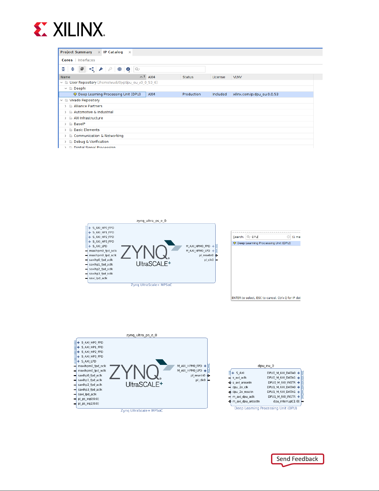
Add DPU IP into Repository
In the Vivado GUI, click Project Manager > IP Catalog. In the IP Catalog tab, right-click and select Add
Repository (Figure 17), then select the location of the DPU IP. This will appear in the IP Catalog page
(Figure 18).
Figure 17: Add Repository
DPU IP Product Guide www.xilinx.com 28
PG338 (v1.2) March 26, 2019
Page 29
Send Feedback
Figure 18: DPU IP in Repository
Add DPU IP into Block Design
Search DPU IP in the block design interface and add DPU IP into the block design. The procedure is
shown in Figure 19 and Figure 20.
Chapter 5: Development Flow
DPU IP Product Guide www.xilinx.com 29
PG338 (v1.2) March 26, 2019
Figure 19: Search DPU IP
Figure 20: Add DPU IP into Block Design
Page 30

Chapter 5: Development Flow
Send Feedback
Configure DPU Parameters
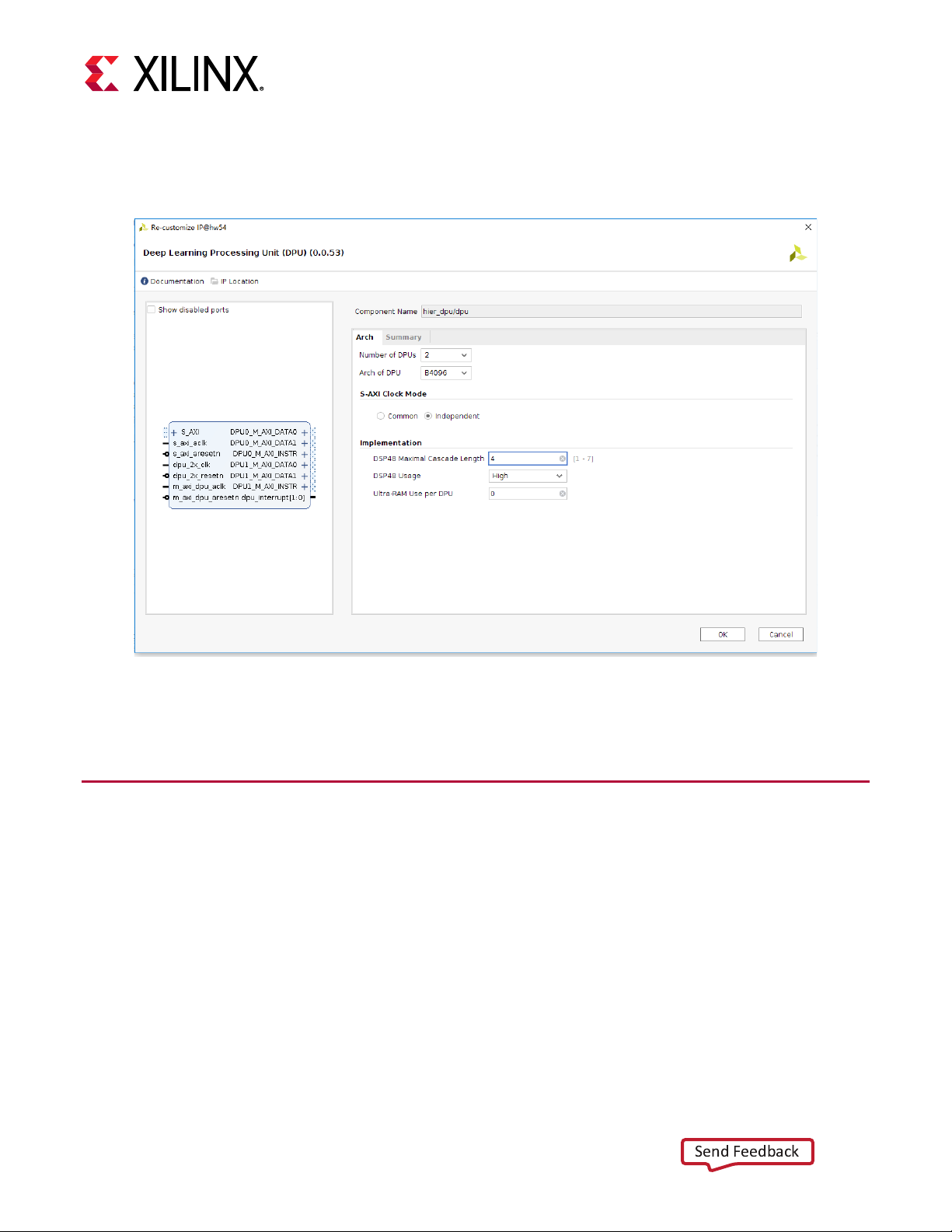
You can configure the DPU IP as shown in Figure 21. The details about these parameters can be found
in
Chapter 3: DPU Configuration
.
Figure 21: Configure DPU
Connect DPU with a Processing System in the Xilinx SoC
No matter how many DPU cores are configured, there is only one slave interface in the DPU IP. Each
DPU core has three master interfaces, one for instruction fetch and the other two for data fetch. The
number of master interfaces in the DPU IP depends on the DPU_NUM parameter.
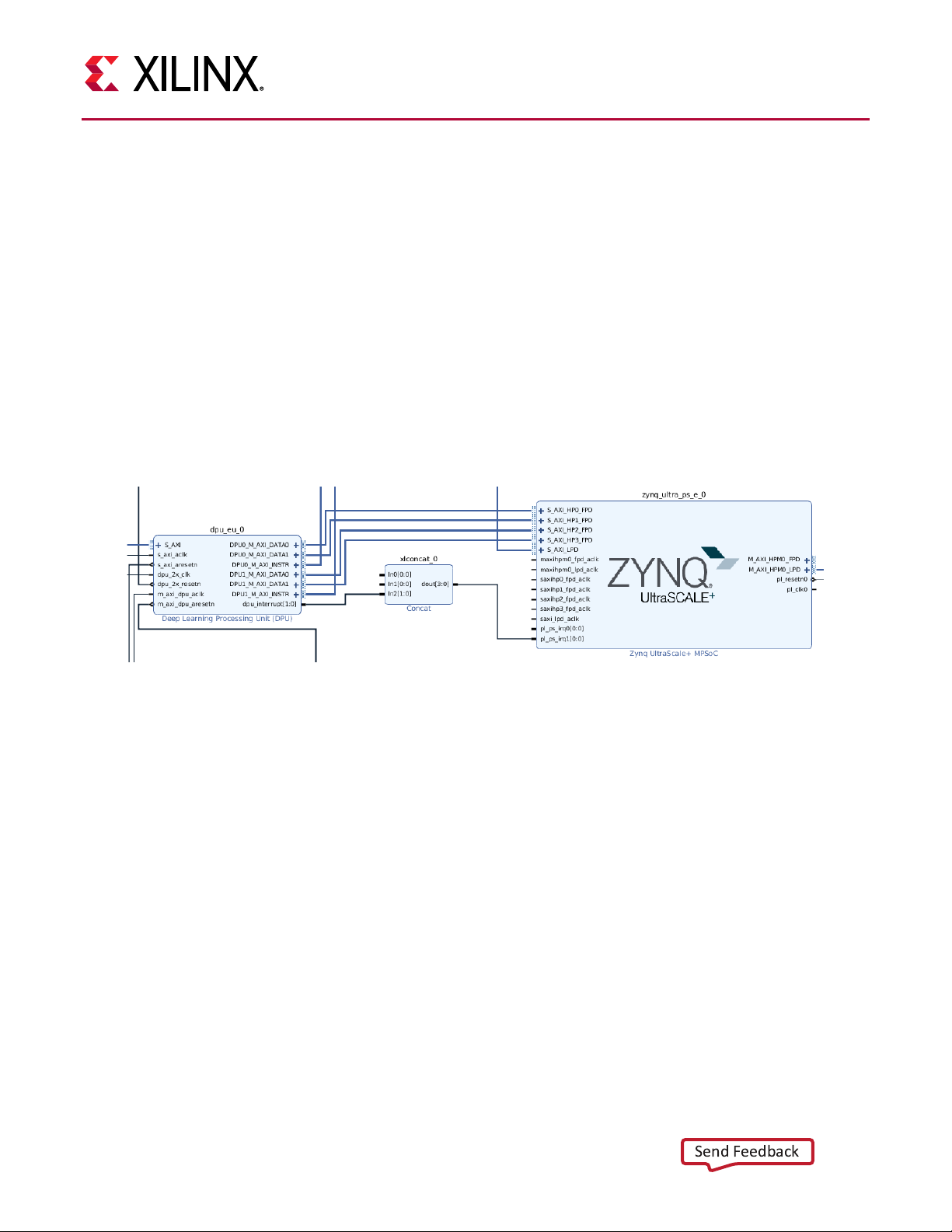
You can connect the DPU to a processing system (PS) with any kind of interconnections. You must
ensure the DPU can correctly access the DDR memory space. Generally, an AXI data transaction passes
an Interconnect IP, the delay of data transaction will increase. The delay of the data transmission
between the DPU and the Interconnect will reduce the DPU performance. Therefore, Xilinx
recommends that each data fetch master interface in the DPU connects to the PS through a direct
connection rather than through an AXI Interconnect IP. The reference connection between the DPU and
PS in the Xilinx UltraScale+™ MPSoC is shown as Figure 22.
®
DPU IP Product Guide www.xilinx.com 30
PG338 (v1.2) March 26, 2019
Page 31

Send Feedback
Chapter 5: Development Flow
Figure 22: Connect DPU with PS of MPSoC
Assign Register Address for DPU
When the DPU connection is complete, the next step is to assign the register address of the AXI slave
interface. The minimum space needed for the DPU is 16 MB. The DPU slave interface can be assigned to
any starting address accessible by the host CPU.
Note: When building a custom system with the pre-built Linux environment in the DNNDK package, the
DPU slave interface must be connected to the M_AXI_HPM0_LPD PS Master and the DPU base address
must be set to 0x8F00_000 with a range of 16 MB. The DPU register address in the driver and device tree
file in the DNNDK package is fixed at 0x8F00_0000. If the address in the driver and device tree file is the
same as the address assigned in Vivado, you can connect the DPU slave interface to any master interface
in the PS and allocate any address for the DPU.
The reference address assignments of the DPU with the DNNDK package are shown in Figure 23.
DPU IP Product Guide www.xilinx.com 31
PG338 (v1.2) March 26, 2019
Page 32

Chapter 5: Development Flow
Send Feedback
Figure 23: Assign DPU Address
Generate Bitstream
Click Generate Bitstream in Vivado shown in Figure 24.
Figure 24: Generate Bitstream
Generate BOOT.BIN
You can use the Vivado SDK or PetaLinux to generate the BOOT.BIN file. For boot image creation using
the Vivado SDK, refer to the Zynq UltraScale+ MPSoC Embedded Design Tutorial (UG1209). For
PetaLinux, use the PetaLinux Tools Documentation Reference Guide (UG1144).
DPU IP Product Guide www.xilinx.com 32
PG338 (v1.2) March 26, 2019
Page 33

Send Feedback
Chapter 6: Example Design
Introduction
The Xilinx® DPU targeted reference design (TRD) provides instructions on how to use DPU with a Xilinx
SoC platform to build and run deep neural network applications. The TRD uses the Vivado® IP
integrator flow for building the hardware design and Xilinx Yocto PetaLinux flow for software design.
The Zynq® UltraScale+™ MPSoC platform is used to create this TRD. It can also be used for a Zynq7000 SoC platform with the same flow.
This appendix describes the architecture of the reference design and provides a functional description
of its components. It is organized as follows:
• DPU TRD Overview provides a high-level overview of the Zynq UltraScale+ MPSoC device
architecture, the reference design architecture, and a summary of key features.
• Hardware Design Flow gives an overview of how to use Xilinx Vivado Design Suite to generate
the reference hardware design.
• Software Design Flow describes the design flow of project creation in the PetaLinux
environment.
• Demo Execution describes how to run the application created by the TRD.
DPU TRD Overview
The TRD creates an image classification application running a popular deep neural network model,
Resnet50, on a Xilinx UltraScale+ MPSoC device. The overall functionality of the TRD is partitioned
between the Processing System (PS) and Programmable Logic (PL), where DPU resides for optimal
performance.
The following figure shows the TRD block diagram. The host communicates with the ZCU102 board
through Ethernet or UART port. The input images for a TRD are stored in an SD card. When the TRD is
running, the input data is loaded into DDR memory, then DPU reads the data from the DDR memory
and writes the results back to DDR memory. The result displays on the host screen from the APU
through Ethernet or UART port.
DPU IP Product Guide www.xilinx.com 33
PG338 (v1.2) March 26, 2019
Page 34

Chapter 6: Example Design
Send Feedback
Figure 25: DPU TRD Overview
The application code used in the DPU TRD is from main.cc in the Resnet50 example in the DNNDK
package. For more information about the DNNDK package, refer to the DNNDK User Guide (UG1327).
Requirements
The following summarizes the requirements of the TRD.
Target platforms:
• ZCU102 evaluation board, production silicon. See ZCU102 Evaluation Board User Guide
(UG1182).
Xilinx tools:
• Vivado Design Suite 2018.2
• PetaLinux 2018.2
Hardware peripherals:
• SD
• Ethernet
• UART
Linux or Windows host system:
• Serial terminal
• Network terminal
DPU IP Product Guide www.xilinx.com 34
PG338 (v1.2) March 26, 2019
Page 35

Send Feedback
Design Files
Design files are in the following directory structure.
Chapter 6: Example Design
Note: DPU_IP is in the
pl/srcs/dpu_ip/
Figure 26: Directory Structure
directory.
DPU IP Product Guide www.xilinx.com 35
PG338 (v1.2) March 26, 2019
Page 36

Chapter 6: Example Design
Send Feedback
Hardware Design Flow
This section describes how to create the DPU reference design project in the Xilinx Vivado Design Suite
and generate the bit file. The parameters of DPU IP in the reference design are configured accordingly.
Both the connections of the DPU interrupt and the assignment addresses for DPU in the reference
design should not be modified. If those connections or assignment address have been modified, the
reference design might not work properly.
Board Setup
The following figure shows the ZCU102 board with interfaces identified.
DPU IP Product Guide www.xilinx.com 36
PG338 (v1.2) March 26, 2019
Figure 27: ZCU102 Board
Page 37

Send Feedback
ZCU102 Board Configuration
1. Connect the Micro USB cable into the ZCU102 Board Micro USB UART (J83) and the other end into
an open USB port on the host PC. This cable is used for UART over USB communication.
2. Insert the SD card with the content of image folder into the SD card slot.
3. Set the SW6 switches and configure the boot setting to boot from SD as shown here.
Figure 28: Boot from SD
4. Connect 12V power to the ZCU102 6-Pin Molex connector.
Chapter 6: Example Design
5. Switch on SW1 to power on the ZCU102 board.
Project Build Flow
This section is about how to build the reference Vivado project with Vivado 2018.2. For information
about setting up your Vivado environment, refer to the Vivado Design Suite User Guide (UG910).
Building the hardware design consists of the following steps:
Building the Hardware Design on Linux
1. Open a Linux terminal.
2. Change the directory to
3. Create the Vivado IP integrator project and invoke the GUI by running the following command:
% vivado -source scripts/trd_prj.tcl
Building the Hardware Design on Windows
1. Select Start > All Programs > Xilinx Design Tools > Vivado 2018.2 > Vivado 2018.2.
2. On the Quick Start screen, click Tcl Console.
$TRD_HOME/pl.
3. Type the following command in the Tcl console:
DPU IP Product Guide www.xilinx.com 37
PG338 (v1.2) March 26, 2019
cd $TRD_HOME/pl
source scripts/trd_prj.tcl
After running the scripts, the Vivado IP integrator block design appears as shown in the following
figure.
Page 38

Chapter 6: Example Design
Send Feedback
Figure 29: TRD Block Design
4. In the GUI, click Generate Bitstream to generate the bit file, as shown in the following figure.
DPU IP Product Guide www.xilinx.com 38
PG338 (v1.2) March 26, 2019
Figure 30: Generate Bitstream
Page 39
Send Feedback
Chapter 6: Example Design
DPU Configuration
The version of the DPU IP integrated in the TRD is DPU_v1.3.0. The default parameters of DPU in the
reference design project is shown in the following figure.
Figure 31: DPU Configuration Page
Those parameters of DPU can be configured in case of different resource requirements. For more
information about DPU and its parameters, refer to
Chapter 3: DPU Configuration
.
Software Design Flow
This section shows how to generate BOOT.BIN using the PetaLinux build.
PetaLinux Design Flow
Install PetaLinux
Install PetaLinux as described in the PetaLinux Tools Documentation Reference Guide (UG1144).
DPU IP Product Guide www.xilinx.com 39
PG338 (v1.2) March 26, 2019
Page 40

Chapter 6: Example Design
Send Feedback
Set PetaLinux Variable
Set the following PetaLinux environment variable $PETALINUX:
% source <path/to/petalinux-installer>/Petalinux-v2018.2/petalinux-v2018.2final/settings.sh
% echo $PETALINUX
% export TRD_HOME=<path/to/downloaded/zipfile>/zcu102-dpu-trd-2018-2
Build the PetaLinux Project
Use the following commands to create the PetaLinux project:
% cd $TRD_HOME/apu/dpu_petalinux_bsp
% petalinux-create -t project -s xilinx-dpu-trd-zcu102-v2018.2.bsp
% cd zcu102-dpu-trd-2018-2
% petalinux-config ––get-hw-description=$TRD_HOME/pl/pre-built --oldconfig
% petalinux-build
If the pre-built design is needed, use the ––get-hw-description path below.
If the new generated/modified design is needed, change the $TRD_HOME/pl/pre-built path to
$TRD_HOME/pl/prj/zcu102.sdk/.
Create BOOT.BIN
Use the following to create the BOOT.BIN file:
% cd images/linux
% petalinux-package --boot --fsbl zynqmp_fsbl.elf --u-boot u-boot.elf --pmufw
pmufw.elf --fpga system.bit
This section describes how to run the executables generated by the TRD. Connect to ZCU102 board
through UART or Ethernet. Note the login/password on the ZCU102 board is
root/root.
Build the Demo
This section describes how to build the resnet50 example from the source. The pre-built resnet50 under
$TRD_HOME/images can be used to skip this step. The following example runs on one of the DPU
cores only. For a multi-threading example, refer to the DNNDK User Guide (UG1327).
1. First, extract the SDK:
% cd $TRD_HOME/apu/apps
% ./sdk.sh -d ./sdk -y
You can use the pre-generated sdk.sh under $TRD_HOME/apu/apps or use petalinux-build
-s to generate your own sdk.sh. If the permission is denied running sdk.sh, run chmod 777
sdk.sh.
2. Build the resnet50:
DPU IP Product Guide www.xilinx.com 40
PG338 (v1.2) March 26, 2019
% cd $TRD_HOME/apu/apps/resnet50
% make
Page 41

Send Feedback
Demo Execution
To run the demo:
Chapter 6: Example Design
1. After generating the BOOT.BIN file, copy BOOT.BIN and image.ub (which is in
image/linux folder)
to the SD card.
2. Copy the common directory in $TRD_HOME/images to the SD card.
3. Copy the pre-built resnet50 in $TRD_HOME/images/resnet50 or the newly generated resnet50 in
$TRD_HOME/apu/apps/resnet50/build to the resnet50 directory on the SD card (for example,
/home/resnet50). If the directory does not exist, create a new directory.
4. Insert the SD card into the ZCU102 and boot up the board. After the Linux boot, run as follows:
% cd /home/resnet50/
% ./resnet50
The screenshot is shown in Figure 32.
The input images name is displayed in each line beginning with “Load image”, followed by the expected
result of the input image. The predicted results of DPU is below, and the top-5 prediction probability of
image classification are printed. If the Top-0 predict results are the same as the expected result, then
the DPU is working properly.
DPU IP Product Guide www.xilinx.com 41
PG338 (v1.2) March 26, 2019
Page 42

Chapter 6: Example Design
Send Feedback
Figure 32: Running Results
DPU IP Product Guide www.xilinx.com 42
PG338 (v1.2) March 26, 2019
Page 43

Send Feedback
Appendix A: Legal Notices
References
These documents provide supplemental material useful with this product guide:
1. DNNDK User Guide (UG1327)
2. Zynq UltraScale+ MPSoC Embedded Design Tutorial (UG1209)
3. PetaLinux Tools Documentation Reference Guide (UG1144)
4. ZCU102 Evaluation Board User Guide (UG1182)
Please Read: Important Legal Notices
The information disclosed to you hereunder (the “Materials”) is provided solely for the selection and use of Xilinx products. To the maximum
extent permitted by applicable law: (1) Materials are made available "AS IS" and with all faults, Xilinx hereby DISCLAIMS ALL WARRANTIES
AND CONDITIONS, EXPRESS, IMPLIED, OR STATUTORY, INCLUDING BUT NOT LIM ITED TO WARRA NTIES OF MERCHAN T ABILIT Y,
NON-INFRINGEMENT, OR FITNESS FOR ANY PARTICULAR PURPOSE; and (2) Xilinx shall not be liable (whether in contract or tort,
including negligence, or under any other theory of liability) for any loss or damage of any kind or nature related to, arising under, or in
connection with, the Materials (including your use of the Materials), including for any direct, indirect, special, incidental, or consequential loss
or damage (including loss of data, profits, goodwill, or any type of loss or damage suffered as a result of any action brought by a third party)
even if such damage or loss was reasonably foreseeable or Xilinx had been advised of the possibility of the same. Xilinx assumes no
obligation to correct any errors contained in the Materials or to notify you of updates to the Materials or to product specifications. You may not
reproduce, modify, distribute, or publicly display the Materials without prior written consent. Certain products are subject to the terms and
conditions of Xilinx’s limited warranty, please refer to Xilinx’s Terms of Sale which can be viewed at https://www.xilinx.com/legal.htm#tos; IP
cores may be subject to warranty and support terms contained in a license issued to you by Xilinx. Xilinx products are not designed or
intended to be fail-safe or for use in any application requiring fail-safe performance; you assume sole risk and liability for use of Xilinx products
in such critical applications, please refer to Xilinx’s Terms of Sale which can be viewed at https://www.xilinx.com/legal.htm#tos.
AUTOMOTIVE APPLICATIONS DISCLAIMER
AUTOMOTIVE PRODUCTS (IDENTIFIED AS “XA” IN THE PART NUMBER) ARE NOT WARRANTED FOR USE IN THE DEPLOYMENT OF
AIRBAGS OR FOR USE IN APPLICATIONS THAT AFFECT CONTROL OF A VEHICLE (“SAFETY APPLICATION”) UNLESS THERE IS A
SAFETY CONCEPT OR REDUNDANCY FEATURE CONSISTENT WITH THE ISO 26262 AUTOMOTIVE SAFETY STANDARD (“SAFETY
DESIGN”). CUSTOMER SHALL, PRIOR TO USING OR DISTRIBUTING ANY SYSTEMS THAT INCORPORATE PRODUCTS,
THOROUGHLY TEST SUCH SYSTEMS FOR SAFETY PURPOSES. USE OF PRODUCTS IN A SAFETY APPLICATION WITHOUT A
SAFETY DESIGN IS FULLY AT THE RISK OF CUSTOMER, SUBJECT ONLY TO APPLICABLE LAWS AND REGULATIONS GOVERNING
LIMITATIONS ON PRODUCT LIABILITY.
© Copyright 2019 Xilinx, Inc. Xilinx, the Xilinx logo, Artix, ISE, Kintex, Spartan, Virtex, Zynq, and other designated brands included herein are
trademarks of Xilinx in the United States and other countries. AMBA, AMBA Designer, Arm, ARM1176JZ-S, CoreSight, Cortex, PrimeCell,
Mali, and MPCore are trademarks of Arm Limited in the EU and other countries. PCI, PCIe, and PCI Express are trademarks of PCI-SIG and
used under license. All other trademarks are the property of their respective owners.
DPU IP Product Guide www.xilinx.com 43
PG338 (v1.2) March 26, 2019
 Loading...