

Page 1

INSTRUCTION MANUAL
Model
75
Arbitrary
Waveform Generator
0
1986
Wavetek
This document contains information
proprietary to
Wavetek and is provided solely for instrument
operation and maintenance. The information in this
document may not be duplicated in any manner without the prior approval in writing from Wavetek.
WAVETEIQ
WAVETEK SAN DIEGO, INC.
9045
Balboa Ave.. San Diego, CA
92123
P.
0.
Box
85265.
San Diego. CA
921 38
Tel
61 912792200
TWX
91 013352007
Manual Revision
2/89
Manual Part Number:
1300-00-0366
Scans
by
ArtekMedia
O
2006
Page 2

Scans
BY
Artek
Media
Artek
Media
1042
Plummer
Cir.SW
Rochester,
MN
55902
www
.artekmedia
.co
m
"High
resolution
scans
of
obsolete
technical
manuals"
if
your
looking
foraquality
scanned
technical
manual
in
PDF
format please
visit
our
WEB
site
at
www
.artekmedia
.co
m
or
drop
us
an
email
at
manuals
@
artekme
dia
.co
m
and
we
will
be
happy
to
email
you
a
current
list
of the
manuals
we
have
available
.
If
you
don't
see
the
manualyou
need
on
the
list
drop
us
a
line
anyway
we
may
stillbeable
to
point
you
to
other
sources.If
you
have an
existing
manual
you
would
like
scanned
please
write
for
details,
This
can
often
be
done
very
reasonablyinconsideration
for
adding
your
manual
to
our
library
.
Typically
the
scans
in
our
manuals
are
done
as
follows
;
1)
Typed
text
pages
are
typically
scanned
in
black
and
white
at
300
dpi
.
2)
Photo
pages
are
typically
scanned
in
gray
scale
mode
at
600
dpi
3)
Schematic
diagram
pages
are
typically
scanned
in
black
and
white
at
600
dpi
unless
the
original
manual
had
colored
high
lighting
(asisthe
case
for
some
70's
vintage
Tektronix
manuals)
.
if
you
purchased
this
manual
from
us
(typically
through
our
Ebay
name
of
ArtekMedia)
thank
you
very
much
.Ifyou
received
this
from
a
well-meaning
"friend"
for
free
we
would
appreciate
your
treating
this
much
like
you
would
"share
ware".By
that
we
mean
a
donation
of at
least
$5-10
per
manual
is
appreciated
in
recognition
of
the time
(a
manualcan
take as
much
as40hours
to
reproduce,
book,
link
etc
.),
energy
and
qualityofeffort
that
went
into
preserving
this
manual
.
Donations
via
PayPal
goto:
manmanuals@artekmedia
.co
m
or
can
be
mailedtous
the
address
above
.
Dave&Lynn
Henderson
Artek
Media
Page 3

CONTENTS
SECTION
1
GENERAL DESCRIPTION
1.1 MODEL 75
.................................................
1-1
........................................
1.2 WAVEFORM EDITING 1-1
.......................................
1.2.1 Standard Waveforms 1-1
......................................
1.2.2 Rubber Band Editing 1-1
............................
1.2.3 Digital Amplitude and Digital Offset 1-1
1.2.4 Point Edit
................................................
1-1
......................................
1.3 STANDARD FEATURES 1-1
........................
1.3.1 81 92 x 4095 Point Waveform Resolution 1-1
................................
1.3.2 Crystal Controlled Frequency 1-1
..........................................
1.3.3 Operating Modes 1-1
..................................
1.3.4 Internal Waveform Counter 1-1
1.3.5 Hold Function
.............................................
1-1
...........................................
1.3.6 Return Function 1-2
.........................................
1.3.7 Stored Waveforms 1-2
...............................
1.3.8 Non-Volatile Instrument Set-Up 1-2
...........................................
1.3.9 Series Operation 1-2
.........................................
1.3.1 0 Parallel Operation 1-2
...................................
1.3.1 1 Communications Options 1-2
...........................................
1.4 SPECIFICATIONS 1-2
.......................................
1.4.1 Standard Waveforms 1-2
..........................................
1.4.2 Operational Mode 1-2
.......................................
1.4.3 Waveform Resolution 1-2
..............................................
1.4.4 Sample Rate 1-2
............................................
1.4.5 Output Signals 1-3
......................................
1.4.6 Output Characteristics 1-3
...................................................
1.4.7 Inputs 1-3
1.4.8 Trigger Sources
...........................................
1-3
..............................
1.4.9 Communication Ports (Optional) 1-4
................................................
1.4.10 General 1-4
1.4.11 Options
.................................................
1-4
SECTION
2
INITIAL PREPARATION
....................................
2.1 UNPACKING INSPECTION 2-1
..................................
2.2 ELECTRICAL INSTALLATION 2-1
.........................................
2.2.1 Power Connection 2-1
...................................
2.2.2 Verifying the Line Voltage 2-1
..................................
2.2.3 Fuse and Voltage Selection 2-2
.......................................
2.2.4 Signal Connections 2-3
......................................
2.2.5 Interface Connections 2-3
.............................................
2.2.6 GPlB Address 2-4
......................
2.2.7
RS-232
Baud Rate and DTElDCE Selection 2-4
..............................
2.2.8 Connecting the RS-232 Interface 2-5
..............................
2.3 INITIAL CHECKOUT PROCEDURE 2-7
Scans
by
Artekhledia
O
2006
Page 4

CONTENTS (Continued)
SECTION
3
OPERATION
...
......
3.1 INTRODUCTION
.........
...........
3-1
....
3.2 CONTROLS, CONNECTORS. AND INDICATORS
..........
3-1
.................................
3.3 OPERATION
......
3-7
.......
3.4 INITIAL SETUP
......
................... 3-7
................................
3.5 EDITING WAVEFORMS 3-7
...........................
3.6 THUMBTACKS AND CURSOR 3-8
...........................
3.7 RUBBER BAND EDITING 3-8
3.8 INSERTING STANDARD WAVEFORMS
................ 3-8
3.9 DIGITAL AMPLITUDE
...............................
.
.
3-8
......
.........
3.1 0 NORMALIZING
......
. 3-8
.....
3.11 DIGITAL OFFSET
.............................
3-8
........................................
3.1 2 POINT EDITING 3-8
.............................
3.1 3 START AND STOP ADDRESSES 3-11
............................
3.1 4 WAVEFORM PARAMETERS 3-11
............
3.1 4.1 Waveform Frequency, Period, and Sample Freq 3-11
3.1 4.2 External Reference
................................
3-12
3.1 4.3 Waveform Amplitude
..........................
...
3-12
............................
3.1 4.4 Waveform Offset
...
3-12
................................
3.1 5 OPERATIONAL MODES 3-12
3.1 5.1 Continuous Mode
...............................
. .
3-12
......................................
3.1 5.2 Triggered Mode 3-12
3.15.3 Gated Mode
.............................
........ 3-12
.........................................
3.1 5.4 Toggled Mode 3-12
.....
3.15.5 Burst Mode
.......................
. .
3-1 3
....
3.16 SETTING AND CLEARING BREAK POINTS
...........
3-13
.............................
3.1 7 SYNC ADDRESS AND PHASE 3-13
......
3.1 8 STORllVG AND RECALLING WAVEFORMS
.......
3-13
3.19 CHAINED OPERATION
...............................
3-13
................................
3.20 WAVEFORM COUNTER 3-13
..................................
3.21 WAVEFORM HOLD 3-13
....................................
3.22 RETURN TO START 3-13
................................
3.23 LOW BATTERY INDICATOR 3-14
3.24 SERIES OPERATION
...............................
. 3-14
3.25 PARALLEL OPERATION
....................
...
3-14
.....................
3.26 GPlB CONTROLS (Option 001 Only) 3-15
...........................
3.26.1 GPlB Address DIP Switches 3-15
.........................................
3.26.2 Setup Menu Key 3-15
.........................................
3.26.3 BLIFFR Soft Key 3-15
........................................
3.26.4 ADRS Soft Key 3-15
.....................................
3.26.5 LOCAL Soft Key 3-15
.........................................
3.26.6 Control Knob 3-15
.................
3.27 GENERAL PLIRPOSE INTERFACE BUS (GPIB) 3-16
.................................
3.27.1 Bus Line Definitions 3-17
...................................
3.27.2 Handshake Sequence 3-18
..........................................
3.27.3 Commands 3-18
........................................
3.27.4 Listen Address 3-18
............................................
3.27.5 Talk Address 3-18
....................
.....
...
3.27.6 Secondary Address
..
..
3-18
....................................
3.27.7 Universal Commands 3-18
Scans
by
ArtekMedia
O
2006
Page 5

CONTENTS (Continued)
3.27.8 Addressed Commands
..................................
3-19
3.27.9 Data Transfer
.......................................
3-19
3.28 MODEL 75
GPlB PROGRAMMIIVG
.......................
3-19
3.28.1 General Programming Information
..................
3-19
3.28.2 Characters
.....................................
. . 3-19
3.28.3 Action and Parameter Commands
...............
...
3-20
3.28.4 Action Commands
.....................
.......
3-20
.....
3.28.5 Programming Parameters
......................
3-20
3.28.6 Sending Waveforms to the Model 75
.......
...........
3-20
3.28.7 High Speed Binary Waveform Transfer
.........
3-21
...
3.28.8 Reading Waveforms From the Model 75
...
3-21
..............................
3.28.9 Programming Reference Guide 3-21
...........
3.29 ERRORS - GPlB REPORTING
...........
3-26
............................................
3.29.1 Class 1 Errors 3-26
.........................................
3.29.2 Class 2 Errors 3-27
......................................
3.29.3 Class 3 Errors 3-27
3.30 RS-2326 CONTROLS
.....
. .
.
.
3-27
....
3.30.1 Setup Menu Key 3-27
3.30.2 BUFFR Soft Key
. . .
. 3-28
....................................
3.30.3 LOCAL Soft Key 3-28
...
3.30.4 HAND Soft Key
.
. . .
3-28
..................................
3.30.5 Control Knob 3-28
.........................................
3.30.6 Baud Rate Switch 3-28
...
......
3.31 GENERAL RS-2326 INFORMATION
.....
3-28
......
3.31.1 Characters
......
...
.
. 3-29
.........
3.31.2 RS-2326 Terminators ..... 3-29
............................
3.31.3 Action and Parameter Commands 3-30
.....
3.31.4 Action Commands
. .
.......
.
. 3-30
...
....
3.31.5 Programming Parameters
...........
3-30
.........................
3.31.6 Sending Waveforms to the Model 75 3-31
3.31.7 Reading Waveforms from the Model 75
.....................
3-31
3.31.8 Programming Reference Guide
...........................
3-31
...
3.32 ERRORS - RS-232-C
REPORTING
....................
3-31
3.32.1 Class 1 Errors
........................................
3-31
....
3.32.2 Class 2 Errors
....
3-32
3.32.3 Class 3 Errors
. .....
.....................
3-32
SECTION
4
CIRCUIT DESCRIPTION
4 1 INTRODUCTION 4-1
4 2 DETAILED CIRCUIT DESCRIPTION 4-1
4 2 1
S~gnal Path 4-1
4 2 2
T~m~ng And Tr~gger~ng 4-9
4 2 3 Instrument Control 4-1 2
4 2 4
Commun~cat~on Optlons 4-1 8
4 2 5 Power Supply 4-1 9
Scans
by
ArtekMedia
O
2006
Page 6

CONTENTS (Continued)
SECTION
5
CALIBRATION
SCOPE
................................
5-1
...........
..........................
FACTORY REPAIR
....
..... 5-1
REQUIRED TEST EQUIPMENT
... .................. 5-1
CALIBRATION
.
.
......
........
..............
5-1
AMPLITUDE
..................... ...........
5-3
OFFSET
....................................
......
5-4
FREQUENCY
..................................
....
5-5
OUTPUT WAVEFORM
RISE AND FALL TIME
.................
5-6
................
SUM IN
........................
5-7
SECTION
6
TROUBLESHOOTING
6.1 FACTORY REPAIR
................................... 6-1
6.2 BEFORE YOU START
..................................
6-1
6.2.1 Isolating a Problem
......................................
6-1
6.2.2 Troubleshooting Dynamic Digital Circuits
....................
6-3
6.3 TROUBLESHOOTING GUIDES
............................... 6-3
6.3.1 Power Supply
...........................................
6-3
6.3.2 Microprocessor and Main Memory
.........................
6-16
6.4 TROUBLESHOOTING
l NDlVlDUAL COMPONENTS
.................
6-20
6.4.1 Transistor
..........................................
3-20
6.4.2 Diode
............................................
6-20
6.4.3 Operational Amplifier
...............................
6-23
6.4.4 Field Effect Transistor (FET)
..............................
6-20
................................
6.4.5 Capacitor
....
6-20
6.4.6 Logic Levels
........................................
6-20
SECTION
7
PARTS LIST AND SCHEMATICS
7.1 DRAWINGS
.......................................
7-1
.............................................
7.2 ERRATA 7-1
7.3 ORDERING PARTS
.................................
7-1
APPENDIX
APPENDIX A AMERICAN STANDARD CODE FOR INFORMATION INTERCHANGE
(ASCII)
.................................................. A-1
APPENDIX B MODEL 75 QUICK REFERENCE GUIDE
.............................
B-1
Scans
by
ArtekMedia
O
2006
Page 7
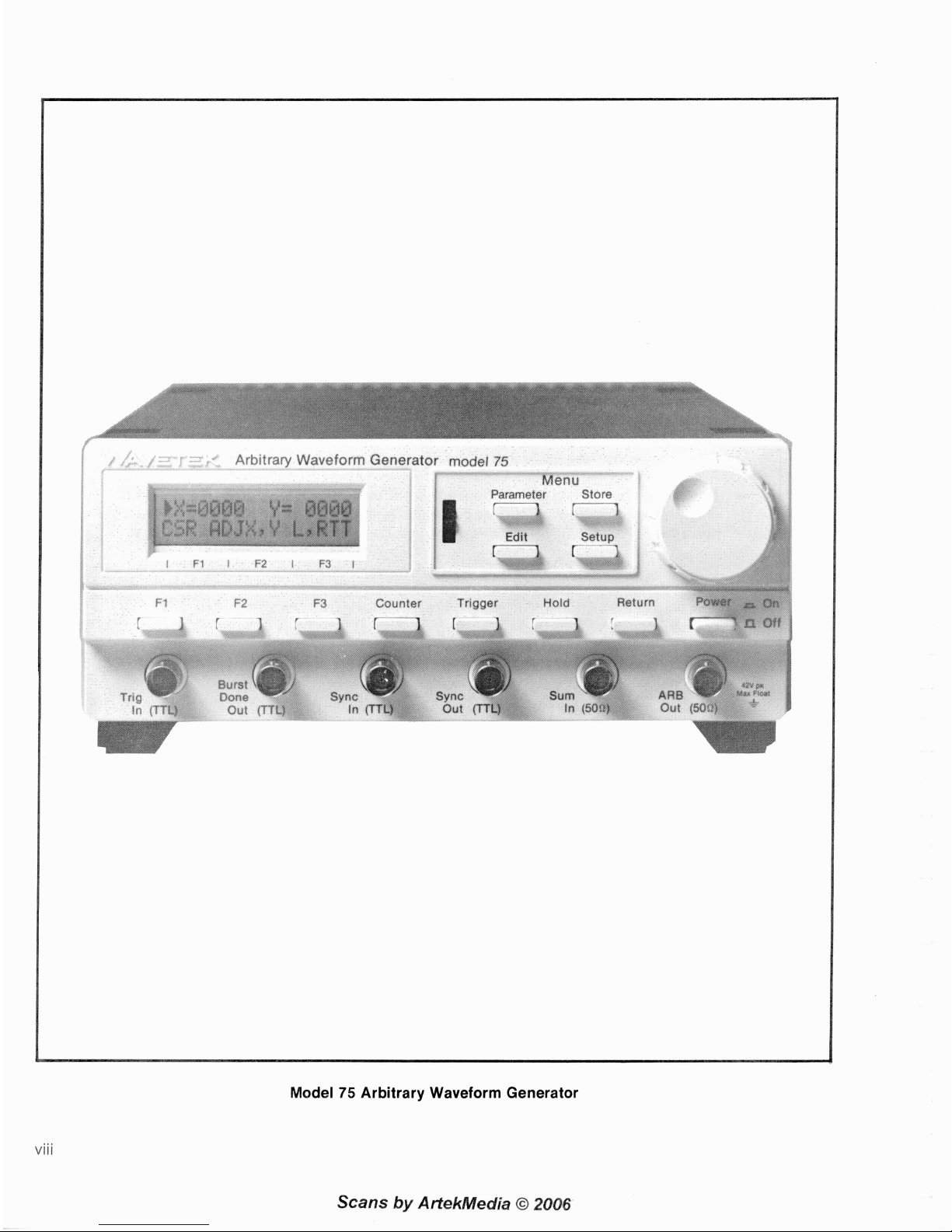
viii
Model
75
Arbitrary Waveform Generator
Scans
by
ArtekMedia
O
2006
Page 8

GENERAL DESCRIPTION
1.1 MODEL 75
The Model 75 is a versatile, yet easy to use arbitrary
waveform generator. It contains advanced waveform
editing features that allow the user to easily create and
edit complex waveforms.
1.2 WAVEFORM EDITING
The editing featuresare based on a pair of points called
"thumbtacks". These thumbtacks are placed at each
end of the portion of the waveform to be edited, then the
appropriate editing feature is invoked. The thumbtacks
will appear as bright dots on an oscilloscope using Z-axis
modulation.
1.2.1 Standard Waveforms
Standard waveforms are inserted between the thumbtacks. Astandard waveform can be the entire waveform
or only part of it. The standard waveforms are sine,
cosine, inverse sine, haversine (inverse cosine), triangle,
square, ramp up, ramp down, and dc. These standard
waveforms can then be edited using the other editing
features if desired.
1.2.2 Rubber Band Editing
Rubber band editing is analogous tostretching a rubber
band between two thumbtacks. A cursor is placed
between the thumbtacks which can be moved in either
theXor they direction.The waveform is then stretched
from each thumbtack to the cursor in real time.
1.2.3 Digital Amplitude and Digital Offset
The sectionof the waveform that is between the thumbtacks can beadjusted in amplitude and offset in real time
without affecting the rest of the waveform.
1.2.4 Point Edit
Individual points of the waveform can also be adjusted
in real time.
1.3 STANDARD FEATURES
1.3.1 81 92 x 4095 Point Waveform Resolution
The waveforms have a vertical resolution of 4095 points
and a horizontal resolution adjustable from 2 to 8192
points. The waveform memory is broken up into four
blocks of 2048 horizontal points. This can be used as one
waveform of up to 8192 points or as four different
waveforms (one active and three stored) of up to 2048
points each.
1.3.2 Crystal Controlled Frequency
The waveform clock (sample frequency) is crystal con-
trolled and adjustable from 20
mHz to 2 MHz (500 ns to
50s), allowing a waveform periodof 1 ps to 11 3.8 hours.
The frequency is adjustable as either waveform frequency, waveform period, or sample frequency. An
external
TTL
level clock of up to 2 MHz can also be used
as the waveform clock (sample freq).
1.3.3 Operating Modes
The Model 75 can operate in continuous, triggered,
gated, toggled, or burst modes. All modes except continuous are initiated (triggered) by either a front panel
pushbutton or an external signal. In these modes the
waveform stops at break points which can be inserted
anywhere in the waveform (by default one breakpoint will
be at the start address), then waits for another trigger.
In burst mode, a predetermined number of waveforms
(from
1
to 1,048,575) is generated before stopping.
1.3.4 Internal Waveform Counter
In gated, toggled, and burst modes an internal counter
can be used to display the number of complete
waveforms since the last trigger. This is particularly
useful for monitoring a burst of waveforms or counting
the number of waveforms for fatigue testing.
1.3.5 Hold Function
A front panel pushbutton or external signal will cause
the waveform to stop at the current output level and
remain there until the hold is released.
Scans
by
ArtekMedia
O
2006
Page 9

1.3.6 Return Function
A front panel pushbutton or external signal will cause
the output to ramp back to the start value. The rate of
this ramp is adjustable from
0 (instant return tostart) to
100 ms per vertical point.
1.3.7 Stored Waveforms
Three additional waveforms may be stored (with their
parameter settings) in waveform memory. These may
later be recalled into, or exchanged with the active
waveform. This feature is only available with horizontal
resolutions of 2048 points or less.
1.3.8 Nonvolatile Instrument Setup
The complete instrument setup is stored in battery
backed up memory so that it will not have to be reset
after the power has been turned off.
1.3.9 Series Operation
Several Model 75's can be connected in series, each one
producing a burst of waveforms, with their outputs
summed together (using the "sum in" connector). This
can be used to produce long waveforms or unusual
sequences such as 50 "normal" waveforms and then
1 "abnormal" waveform.
1.3.1 0 Parallel Operation
Several Model 75's can be connected in parallel to create
phase coherent arbitrary waveforms. The phase relationship is completely adjustable with a resolution equal to
the horizontal resolution of the waveform. This feature
is useful in three axis mechanical testing and multi-phase
power applications.
1.3.1 1 Communications Options
Either an IEEE-488or RS232Ccommunication interface
is available to transfer waveform data and control the
Model 75 from a computer.
1.4 SPECIFICATIONS
1.4.1 Standard Waveforms
DC, square, triangle, up-ramp, down-ramp, sine, cosine,
inverse sine, and haversine waveforms are provided.
Each of these waveforms can be stored into the
waveform memory between thumbtacks automatically,
and then edited with the waveform editing functions if
desired.
1.4.2 Operational Modes
Continuous
Output runs repetitively from the programmed start
address to the programmed stop address.
Triggered
Output quiescent until triggered by external signal or
front panel pushbutton, then runs until another break
point is encountered. Break points can be inserted
anywhere in the waveform with the default break point
at the beginning of the waveform.
Gated
Same as triggered mode except that the output is continuous for the duration of the gate signal and until the
first break point encountered after the gate signal ends.
Burst
Same as in the triggered mode except that a program-
mable number of waveforms is counted before the
waveforms stop. The maximum burst is 1,048,575
waveforms.
Toggled
The output is quiescent until triggered. It then runs continuously until another trigger stops the waveform at the
next break point.
1.4.3 Waveform Resolution
Normal Waveform
2048 points horizontal
x
4095 points vertical.
Chained Waveform
81 92 points horizontal
x
4095 points vertical. Stored
waveforms are not available with chained operation.
1.4.4 Sample Rate
Range
0.02 Hz to 2.0 MHz (50
s to 500 ns)
Waveform Period and Frequency
The actual waveform period is the number of horizontal
points (from start to stop address) times the sample time.
This can range from 1 microsecond for a square wave
to 11 3.8 hours for a waveform using all 81 92 points.
Frequency Resolution
4 digits
Frequency Accuracy
+
0.01 5
'10
Repeatability (24 Hr)
+
25 ppm
Temperature Coefficient
<5 ppml°C
Scans
by
Artekhledia
O
2006
Page 10

1.4.5
Output Signals Z-Axis Out
Amplitude
This signal is a pulse, adjustable in amplitude from 2 to
14 volts, that is used to modulate the Z-axis of an
Range:
+
0.005 to 5 Vp into 509 (0.01 to 10 VP-P into
oscilloscope when using the waveform editingfeatures.
509). + 0.01 to 1 OVp into an open circuit (0.02 to 20Vp-p
The logic polarity is also selectable.
into an open circuit).
Resolution: 3 digits.
Accuracy:
+
1.8% of setting and + 2.5 mVfor amplitude
1.4.7
Inputs
+
offset 20.5V.
k
1.8% of setting and ? 0.25 mV for 0.5V > amplitude
sum
In (509)
+
offset 250 mV.
The signal at this input is added to the arbitrary waveform
+
1.8% of setting and + 25 pV for 50 mV > amplitude
to produce an output (at waveform out)of the sum of the
+
offset.
two. A peak input of
+
5V w~ll produce an output equal
Repeatability (24 Hr):
k
0.1
O/O
of setting.
to the amplitude setting. Input is fuse protected.
Tem~erature Coefficient: 61 50 ppml°C of setting.
Accuracy is
4% (2% if internal fuse is shorted).
Offset
Trig In (TTL)
lm~edance is 100 KR. Sianal is used to control the
Range:
+
5~ to - 5V into 50R
(-
10V to + 1 OV into an
ge"erator in the trigger, gaie, toggle, and burst modes.
open circuit). Absolute amplitude
PIUS
offset may not
Slope polarity is selectable,
exceed + 5V into 50R
(+
10V into an open circuit).
Svnc In
(TTL)
Resolution: 3 digits.
lkpedanbe is 100 KR. A high input causes the waveform
Accuracy:
2% of setting and + 15 mV for amplitude
+
to restart at the start address. Primarily used for syn-
offset
20.5V.
chronizing several arbitrary waveform generators in
2% of setting and k 1.5 mVfor 0.5V>amplitude + off-
parallel operation.
set 250
mV.
Ref In (TTL)
2% of setting and + 0.1 5 mV for 50 mV > amplitude
+
Impedance is 100 KR. This signal input is used for the
offset.
sample clock when the external ref is selected.
Repeatability (24 Hr):
+
5 mV and + 0.1
O/O
of setting.
Temperature Coefficient:
6(+
1 mV + 150 ppm)l°C of
setting.
1.4.6
Outputs
ARB Out
(50R)
Source of primary waveform output.
Maximum
amplitude is
+
5 Vp into 50R. Output is fuse protected.
Sync Out
(TTL)
Will drive up to 10 LSTTL loads.This is a pulse 1 sample
time wide that is usually used to sync an oscilloscope
or another ARB generator. Pulse position is adjustable
to any point in the waveform.
Burst Done Out (TTL)
Will drive up to 10 LSTrL loads. ATTL low indicates that
the waveform is running. TTL high indicates that the
instrument is waiting for a trigger in triggered, gated,
toggle, or burst modes. Used primarily to start another
ARB generator in series operation.
Ref Out (TTL)
Will drive up to 10 LSTTL loads. This pulse train at the
sample frequency is used primarily as a reference
source for other ARB generators in series operation or
in parallel operation.
Hold In
Impedance is 100 KR. ATTL low or switch closure at this
input causes the generator to stop at the current output
level and remain there until released by a TTL high or
switch opening.
Return In
Impedance is 100 KR.
ATTLlowor switch closureat this
input causes the output level to ramp back to the start
value.
'The ramp rate is front panel selectable from 0 to
100 ms per point.
1.4.8
Trigger Sources
Manual
Use the Trigger pushbutton switch on front panel to
operate internal trigger circuitry. The slope polarity can
be set via the display menus.
External
Use the communication
ports(GPIB or RS-232C)or the
Trig In connector on front panel. Trig In connector frequency input can be up to 1 MHz. The slope polaritycan
be set via the display menus.
Scans
by
ArtekMedia O 2006
Page 11
1.4.9 Waveform Characteristics
Horizontal Resolution
Up to 81 92 points.
Vertical Resolution
4095 bits
(
-
2047 to + 2047).
RiselFall Time
<350 ns.
1.4.10 Communication Ports (Optional)
IEEE-488 Port (Option 001)
Type:
IEEE-488-1978 compatible, non-isolated, double
buffered.
Address: 0-30, internal DIP switch selectable or front
panel selectable.
Subsets:
SHl, AHl, T6, TEO, L4, SRl, RLI, PPO, DCl,
CO. El.
RS-232-C Serial Port (Option 002)
Communication is full duplex
(bi-directional) with
CTSIDTR or XONIXOFF handshaking.
Connector: Rear panel mounted DB-25 (female) with
DCE or DTE configuration.
Data Format: 8 bits, no parity, one stop bit
Data Rate: 14 steps internal switch selectable (50, 75,
1
10,134.5,150,200,300,600,1200,1800,2400,4800,
9600, 19,200).
1.4.1 1 General
Environmental
Temperature Range: + 23°C + 5°C for specified operation, operates
0 to + 50°C, - 20 to + 75°C for storage.
WarmupTime: 20 minutes for specified(guaranteed for
1 year) operation.
Vibration: 5 to 55 Hz with maximum of
29 at 55 Hz.
Shock:
309, 11 ms half sine.
Altitude: Sea level to 10,000 ft. for operation. Sea level
to 40,000 ft. for storage.
Relative Humidity:
95% at 25°C and at sea level
(non-condensing).
Dimensions: 21 cm (8.27 in.) wide,
10 cm (3.94 in.) high,
32.3 cm (1 2.72 in.) deep.
Weight: 3.55 kg (7.8 Ib) net, 4.68 kg (1 0.3 Ib) shipping.
Power: 90 to 128,180 to 256 rms; 48 to 66 Hz; 1 phase;
<25 VA.
1.4.1 2 Options
001: IEEE-488 (GPIB) Port
For instrument control or entering waveform data.
002:
RS-232-C Serial Port
For instrument control or entering waveform data.
NOTE
Options
001
and
002
are mutually exclusive.
Scans
by
ArtekMedia
O
2006
Page 12

INITIAL PREPARATION
2.1 UNPACKING INSPECTION
After carefully unpacking the instrument, visually inspect
all external parts for possibledamage toconnectors, surface areas, etc. If damage is discovered, filea claim with
the carrier who transported the unit. The shipping container and packing material should be saved in case
reshipment is required.
2.2 ELECTRICAL INSTALLATION
2.2.1 Power Connection
WARNING
To preclude injury
ordeath due toshock, the
third wire earth ground must be continuous
to the facility power outlet. Before connect-
ing to the facility power outlet, examine
extension cords, autotransformers, etc.,
between the instrument and the facility power
outlet for acontinuous earth ground
path.The
earth ground path can be identified at the plug
on the instrument power cord; of three terminals, the earth ground terminal is the nonmatching shape, usually cylindrical.
CAUTION
To prevent damage to the instrument, check
for proper match of line and instrument
voltage and proper fuse type and rating.
Line Voltage
Refer to table 2-1 to determine the proper selection of
the line voltage connector. Unless otherwise specified
at the time of purchase, this instrument was shipped from
the factory with the power transformer connected for
operation on a
1 1
5
Vac line supply and with a 318 amp
fuse. If the unit is shipped for
11
5
Vac operation, there
will be no markings or tags on the unit. If the unit is
shipped for 220
Vac operation, there will be a 220 Vac
tag on the rear panel of the unit and a 3/16 amp fuse
installed.
2.2.2 Verifying the Line Voltage
To verify the line voltage (or change the fuse), the
operator must first remove the top and bottom covers.
Remove the top and bottom using the following steps and
figure 2-1.
1. Remove two (2) screws holding top and bottom
covers to rear panel.
2. Slide both covers (together as a unit) to the rear and
remove from the chassis assembly.
Figure 2-1. Top and Bottom Cover Removal
After the covers have been removed, the line voltage can
be checked by viewing the voltage label through the
inspection hole as shown in figure 2-2.
INSPECTION SLOT
GUARD PLATE
'
REAR PANEL
Figure 2-2. Line Voltage Inspection Hole
Scans
by
ArtekMedia
O
2006
Page 13

2.2.3 Fuse and Voltage Selection
If
the line voltage is not correct according to table 2-1,
perform the following steps and refer to figure 2-3 for
steps 1 and 2, and figure 2-4 for steps 3 thru 6
tochange
the line voltage and fuse.
1. Remove the two screws holding guard plate to the
rear panel.
2. Remove the guard plate from the rear panel.
GUARD
PLATE
SCREWS
/
VOLTAGE
SELECTOR
CONNECTOR
F
U
AC
PRIMARY
-
VOLTAGE
SELECTOR
Figure 2-3. Guard Plate Removal
Figure 2-4. Fuse and Voltage Selection
3. Remove the voltage selector connector from the ac
primary board. Rotate the connector until the correct voltage selector indicator is on top.
4. Reinstall the voltage selector connector.
5. Remove the fuse and install new fuse as called out
in table
2-1.
Connector Voltage
Position Range
90
to 128 Vac 318 amp
Table 2-1. VoltagelFuse Selection
220V
WARNING
Because lethal voltages are exposed, do
not apply ac power to the unit until the
guard plate is attached to the unit.
Reassembly
Refer to figure 2-5 for step 1 and figure 2-6 for steps 2
thru 5.
1. Insert the guard plate over the ac primary board and
voltage selector connector and align with screw
holes in the rear panel. Secure with two screws.
180
to
256 Vac
BOARD
311 6 amp
Figure 2-5. Rear Chassis Assembly
Scans
by
ArtekMedia
63
2006
Page 14

Figure
2-6.
Top and Bottom Cover Installation
2. Turn the instrument upside down, position the
bottom cover over the guard shield and rear panel.
Slide the bottom cover forward approximately two
(2) inches while engaging the
topcover shield slides
(see figure 2-6, detail A) and the outside slide rails
(see figure 2-6, detail B).
3.
Turn the instrument right side up. Install the topcover
using the same procedure as in step
2.
4. Align the rear of both the topand bottom cover with
each each other so that the cover interlocks are
properly mated. Once mated, hold the covers firmly
together and slide the chassis assembly into top and
bottom covers.
CAUTION
When sliding on the bottom cover, avoid
moving the ribbon cables located
nearthe
power transformer.
5. Secure covers to unit using two screws as shown
in figure 2-1
.
2.2.4
Signal Connections
Use RG58U 509 coaxial cables equipped with BNC connectors to distribute signals when connecting this instrument to associated equipment.
NOTE
Signal ground may be floated up to
_t
42V
with respect to chassisground. Bea ware that
all signal grounds are common and must all
be floated together.
2.2.5
Interface Connections
The GPlB (Option 001) 110 rear panel connector is an
Amphenol 57-10240 or equivalent and connects to a
GPlB bus cable connector (available from Wavetek in
1 and 2 meter lengths).
NOTE
The terms
"GP1B"and "IEEE-488"are used
synonymously in this manual.
Scans
by
Artekhledia
O
2006
Page 15

2.2.6 GPlB Address
For Option 001 instruments on the General Purpose
Interface Bus (GPIB), ensure that the instrument GPlB
address is correct. The GPlB default address can be
changed by resetting the internal DIP switch (for access,
remove the top cover, see paragraphs 2.2.2 and 2.2.3)
or changed temporarily by pressing the front panel ADRS
soft key and rotating the Control knob when the GPlB
address is displayed.
The switch sections are labeled from 1 thru 5 and their
OPEN position noted (OPEN
=
Binary "0" in table 2-2).
To verify the address, press ADRS soft key on the front
panel.
Table 2-2. GPlB Address Code
Device / Listen I Talk
1
1
2
3
4 5
Listen
1
Talk
2.2.7 The RS-2324 Connectors
The RS-232C 110 rear panel pin connections and signal
names are given in table
2-3. The panel connector is a
DB-25 female connector (see figure 2-7) and will connect to a standard
RS-232C cable (interface type
E).
The data format is an 8-bit, no parity, one stop bit. The
baud rate is selectable from those listed in table 2-5 using
dip switch
S1 (figure 2-8).
Table 2-3. RS-232-C Data InlOut
40
4
1
42
(Remaining Pins Not Connected)
43
'Transmit Data
'Receive Data
3~equest to Send
4~lear to Send
'Data Set Ready
'Receive Line Signal Detect
7~ata Terminal Ready
Pin
2
3
4
5
6
7
8
20
-
/
RS-232-C Connector
Name
TXD'
RXD~
RTS3
CTS~
DSR5
SIG GRD
RLSD'
DTR~
Direction (DCE
Configuration)
IN
OUT
N IC
OUT
OUT
-
OUT
IN
Z-AXIS
out
I60011
1
Ref Ref
Hold
In
Out
In
In
ITTLI ITTL) lTTLl ITTLI
Direction (DTE
Configuration)
OUT
IN
OUT
IN
IN
-
IN
OUT
nnnnnnnnn
Figure 2-7. RS-232-C Connector Pinouts
NOTE:
Address
31
is
not allowed
Scans
by
ArtekMedia
O
2006
Page 16

The following is a description of pin functions. Actual
installation is covered in paragraph 2.2.8.
In the DCE configuration, pins 2 and 3 are data input and
output respectively and must be used. Pin 5 may be used
to indicate that the Model 75 is ready to receive data.
Pin 20 tells the Model 75 that the connected device is
ready to receive data, but may be connected to pin 6 of
the Model 75 if the other device is always ready. Pin 7
is signal ground and must be used. Pins 6 and 8 will be
positive (asserted) when the Model 75 is on.
In the DTE configuration, pins 2 and 3 are data output
and input respectively and must be used. Pin 4 will be
positive whenever the Model 75 is On. Pin 5 tells the
Model 75 that the connected device is ready to receive
data.
If
the other device is always ready, pins 4 and 5
of the Model 75 may be connected together. Pins 6 and
8 are properly terminated inputs but have no function.
Pin
20
will be positive when the Model 75 is ready to
receive data. Pin 7 is signal ground and must be used.
1. Determine if the other device is a DCE device or a
DTE device. If this is not explicitly spelled out you
will need to look at the pin out for its connector. If
pin 2 is the data output, the device is a DTE (most
computers). If pin 3 is the data output, the device
is a DCE (most modems). Configure the Model 75
as the opposite type of device by connecting the
internal optioncable to theappropriate
header(see
figure 2-8).
In most cases a straight through cable can be used
to connect the Model 75 with the other device. The
Model 75 only requires the connection of pins 2, 3,
5,7, and 20 but the other device may require more.
Examples of typical cable assemblies are shown in
figure
2-9. However, there are many interpretations
of the
RS-232Cstandard and either of the following
procedures (a or b) should be used to ensure that
the control and handshake signals are properly
connected.
The handshaking method is front panel selectable as
a. If the Model 75 is configured as a DCE then;
CTSIDTR (hardware) or XONIXOFF (see paragraph 3-32
for more information).
(1) Pin 7 (signal ground) is always connected
straight through.
2.2.8 Connecting the RS-232-C Interface
Before connecting the Model 75 using the RS-232C
interface, the correct configuration (DCE or DTE) must
be selected and the internal ribbon cable connected to
either the DCE or DTE location (see figure 2-8) on the
RS-232-C option board. To determine which configuration is correct, you will need the manual for the device
to which you are connecting the Model 75. The following assumes that the other device has a DB-25,
RS-232-C connector.
DCE
HEADER
Figure 2-8. Baud Rate Switch and DTElDCE
Connections
(2) Pins 2 and 3 are connected straight through
if
DCEIDTE configuration is correct.
(3) Pin 5 of the Model 75 will need to be con-
nected to an input of the other device that
will enable and disable the character
transmission from that device. If the other
device does not support this, XONIXOFF
handshaking will be required and pin 5 can
be left disconnected.
(4) Pin 20 of the Model 75 should be connected
to an output pin on the other device that
indicates when it is ready to accept data.
If the other device does not have such a pin
but is not always ready, it can send
XOFFs
and XONs to indicate readiness. When
using this method, or if the other device is
always ready
toaccept data, this pin can be
connected to an always positive pin on the
other
deviceor topin 60r 8on the Model 75.
(5) Pins 6 and 8 are always positive when the
power is on and can be connected to any
pins on the other device that require being
held positive.
b. If the Model 75 is configured as a DTE then;
(1) Pin 7 (signal ground) is always connected
straight through.
(2) Pins 2 and 3 are connected straight through
if
DCEIDTE configuration is correct.
Scans
by
ArtekMedia
O
2006
Page 17

(3) Pin 20 of the Model 75 will need to be con-
nected to an input of the other device that
will enable (positive) and disable (negative)
the character transmission from that
device. If the other device does not support
this,
XONIXOFF handshaking will be
required and pin
20 can be left dis-
connected.
(4)
Pin 5 of the Model 75 should be connected
to an output pin on the other device that
indicates whether or not it is ready to accept
data. If the other devicedoes not have such
a pin but is not always ready, it can send
XOFFs and XONs to indicate readiness.
When using this method, or if the other
device is always ready to accept data, this
IBM-PC
APPLE
II
WITH SUPER SERIAL CARD
IBM-PC IN COMMUNICATIONS MODE
MODEL 75 MODEL 75
(DCE) APPLE II
DB-25
FEMALE
DB-25 DB-25
MALE MALE
DB-25
MALE
WAVETEK MODEL
6000
APPLE MACINTOSH
6000
MODEL 75 MODEL 75
(DCE) MACINTOSH (DTE)
D 6-25
MALE
D 6-25 DE-9
MALE MALE
Figure
2-9.
Typical Examples
of
Serial Cables
DB-25
MALE
2-6
Scans
by
Artekhledia
O
2006
Page 18

pin can be connected to an always positive
pin on the other device or to pin 4 on the
Model 75.
(5) Pin 4 is always positive when the power is
on and can be connected to any pin on the
other device that requires being held
positive.
(6) Pins 6and 8are properly terminated inputs
but have no function.
NOTE
Anypins not mentioned in the previous list are
not connected in the Model
75and therefore
can be connected to anything if the connections are already present in the cable.
3. The handshaking method is front panel selectable
as
CTSIDTR (hardware) or XONIXOFF (see para-
graph 3.31 for more information).
4. Set the baud
rateon the Model 75 to the highest rate
that is available on both the Model 75 and the other
device by setting the dip switches (figure 2-8)
according to table
2-4.
5. Configure the other device for the same baud rate
as in step 4, 1 stop bit, 8 data bits, and no parity.
Table 2-4. RS-232-C DIP Switch Settings
Baud Rate
SW1-4 SW1-3 SW1-2 SW1-1
Closed
Open
Open
Closed
Open
Open
Closed
Open
Closed
Open
Open
Closed
Open
Closed
Open
Open
Closed
Closed
Open
Closed
Closed
Closed
Open
Open
Closed
Open
1
Open I Closed
Closed
1
(3;:;
I
Closed
Open Open
Closed
Closed
Closed
Open
Closed
Closed
Open
*This is the factory set position
NOTE
1.
SW1-5 should always be OPEN
2.
Factory connector configuration is DCE
Closed
Closed
Closed
Open
Open
Open
Open
Open
Open
Closed
Closed
2.3 INITIAL CHECKOUT PROCEDURE
The Model 75 ARB waveform generator
will
supply a
variety of waveforms at the ARB Out connector that can
be modified at will using the front panel controls. In order
toverify the operation of the controls and the functions1
modeslvalues that they control, the generator must first
be set up to produce an output and then the effect of the
controls on the output and the display indications noted.
While this procedure verifies functional operation of this
instrument, it does not verify the
calibration.Thevalues
shown are typical values and should only be used as a
guide. Required tools and test equipment are shown in
table
2-5.
Closed
Open
Open
Open
Table 2-5. Test Equipment and Tools
Instrument Comments
Oscilloscope
*
50R Feedthrough
BNC Tee
BNC Coax Cable
Signal Source*
Frequency
Counter
Dual channel. 20 MHz rnin bandwidth with external trigger and Zaxis capability.
2% accuracy, 2W
1 male to 2 female
RG58U, Q 3 ft. length (4 each)
1 MHz capability with square
wave (1 0 Vp-p into
50R) and TTL
output.
Capable of both frequency and
period measurements.
*Check the oscilloscope manual to determine the
maximum allowable Z-axis input voltage. Do not
exceed that voltage.
*A second Model 75 can be used as the signal source.
For the TTL signal requirements, use the Ref Out
connector on the rear panel and use the SAMPL
soft key to set the frequency. For the 1 kHz, 10 Vp-p
signal, use the STOP soft key to set the stop address
to 1999, use the FREQ soft key to set the frequency,
and use the FUNC and EXEC soft keys to select a
square wave. See section 3 for more detail.
To verify the overall operation of the Model 75 ARB
waveform generator, follow the procedure in table
2-6.
Refer to the referenced figures and tables for appropriate
test equipment connections and settings. Refer to figure
3-1 and paragraph 3.2 for control and connector
locations.
Scans
by
ArtekMedia
O
2006'
Page 19

Table
2-6.
Checkout Procedure
Step
1
ControllSwitch
Power
PositionlOperation
Press On
ObservationlComments
Display indicates "WAVETEK MODEL 75".
I I
Adjust the LCD viewing control for best contrast.
--
-
-
This step verifies the "Reset" functions of the Model 75.
Press three times
Press once
Press once
2
Display indicates "RESET Ver
x.xx".
Display indicates "RESET Ver x.xx
X".
Setup
F2 (Reset)
F3 (Exec)
This step verifies the "Z-Axis" functions of the Model 75.
Setup
F2 (ZLOGIC)
Control knob
Control knob
F1 (ZLEVL)
Control knob
Control knob
Press once
Press once
Rotate until display
indicates "ZLOGIC
POS".
Rotate until display
indicates "ZLOGIC
NEG".
Press once
Rotate CW until
display indicates
"ZLEVEL
14V".
Rotate CCW to step
display through the
selectable settings.
Connect the Model 75 as shown in figure 2-10. Set
equipment controls as indicated in table
2-7.
Display indicates "ZLOGIC NEG" or "ZLOGIC POS".
Oscilloscope will indicate a dc level of
0
Vdc + 1V
with positive-going pulses.
Oscilloscope will indicate a dc level of
2,
4,
6,
8, 10,
12, or 14 Vdc with negative-going pulses.
Oscilloscope will indicate a dc level of
+
14V
+_
1V
with negative-going pulses.
Oscilloscope will indicate the selected voltage
+_
1V
with negative-going pulses. Leave Setting at "ZLEVEL
2V".
This step sets the "Z-Axis Out" voltage level and polarity.
Control knob Rotate CW or CCW
to set acceptable
contrast between
trace and thumb-
tacks. Adjust oscilloscope intensity if
required.
Connect the Model 75 as shown in figure 2-1 1. Set
equipment controls as indicated in table
2-8.
If thumbtack intensity is too bright at + 2V, terminate
the Z-axis cable with a 50Q load. If the thumbtacks are
dimmed instead of intensified, set ZLOGIC to POS.
Scans
by
ArtekMedia
O
2006
Page 20

Table 2-6. Checkout Procedure (Continued)
This step verifies the "Waveform Memory'' functions of the Model 75.
Store
F2 (CHAIN)
Control knob
ObservationlComments
F3 (EXEC)
Edit
F1 (FUNC)
Control knob
PositionlOperation Step
F3 (EXEC)
ControllSwitch
Edit
F1 (START)
Control knob
Control knob
F2 (STOP)
Control knob
Control knob
Store
F2 (CHAIN)
Control knob
F3 (EXEC)
Edit
F1 (FUNC)
F3 (EXEC)
Press two times
Press once
Rotate until display
indicates "CHAIN
8K".
Press once
Press two times
Press once
Rotate until display
indicates "FUNC
SINE"
Press once
Press two times
Press once
Rotate CW
Rotate CCW
Press once
Rotate CCW
Rotate CW
Press two times
Press once
Rotate until display
indicates "CHAIN
2K".
Press once
Press two times
Press once
Press once
Reset the oscilloscope horizontal sweep to 1
msIDIV.
Oscilloscope will indicate slightly more than one cycle
of the sine wave at approximately 10 Vp-p.
Display will indicate
">ST = 0000 SP = 8191
".
Oscilloscope waveform start point will move from left
to right until waveform disappears. Display will now
indicate
">ST = 81 91 SP = 81 91
".
Oscilloscope waveform start point will move from right
to left until waveform is complete. Display will now
indicate
">ST = 0000 SP = 81 91
".
Display will indicate "ST = 0000 >SP = 81 91.
Oscilloscope waveform stop point will move from right
to left until the waveform disappears. The display will
now indicate "ST
=
0000 >SP = 0000".
Oscilloscope waveform stop point will move from left
to right until the waveform is complete. The display
will
now indicate "ST = 0000 >SP = 81 91
".
Display indicates "CHAIN 8K"
Display indicates "FUNC SINE".
Set the oscilloscope sweep to
.5
mslDIV.
Display will indicate "FUNC SINE X". Oscilloscope
will display less than 3 cycles of a sine wave of approximately 10 Vp-p.
Scans
by
ArtekMedia
O
2006
Page 21

Table
2-6.
Checkout Procedure (Continued)
This step verifies the "Amplitude Control" functions of the Model
75.
Step
This step verifies the "Offset" functions of the Model
75.
ControllSwitch
Display will indicate "AMPL 5.000 Vp".
Oscilloscope amplitude decreases smoothly to
minimum of approximately
10 mVp-p. Display will now
indicate "AMPL 5.00
mVp".
6
This step verifies the "Frequency" functions of the Model
75.
PositionlOperation
7
ObservationlComments
Parameter
F1 (AMPL)
Control knob
Press two times
Press once
Rotate CCW
F2 (OFFSET)
Control knob
Control knob
Control knob
F1 (AMPL)
Control knob
F3 (SAMPL)
Connect a coax cable from the Ref Out connector on
the Model 75 rear panel to the frequency counter input.
Set frequency counter to frequency mode.
Press once
Control knob
Display will indicate "SAMPL 1.0000 MHz'' and counter
will indicate approximately 1 MHz.
Press once
Rotate CW
Rotate CCW
Rotate CW until
display indicates
"OFFSET 0.0
mV".
Press once
Rotate CW until
display indicates
"AMPL 5.000 Vp".
Rotate CCW until
display indicates
"SAMPL 500.0
KHz".
Counter will indicate approximately 500 kHz.
Display will indicate "OFFSET 0.0
mV".
Reset oscilloscope vertical gain to 2VIDIV.
Oscilloscope will increase smoothly to approximately
5.1 OV. The display will now indicate
"OFFSET5.1 OV".
Oscilloscope level decreases smoothly to
approxi-
mately - 5.10V. Display will now indicate "OFFSET
-
5.10V".
Resolution near zero is much greater so that the level
will change slower as zero is approached and passed.
Scans
by
Artekhledia
O
2006
Page 22
Table
2-6.
Checkout Procedure (Continued)
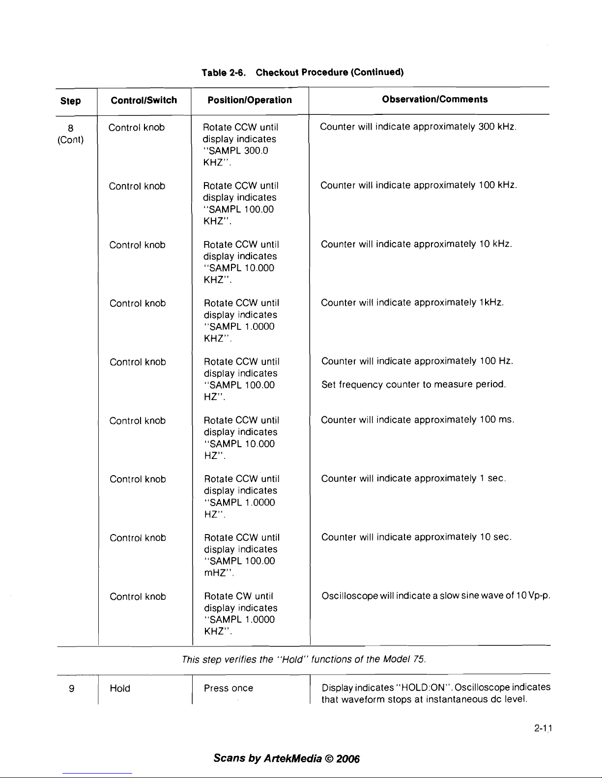
This step verifies the "Hold" functions of the Model
75.
-
9
1
Hold
ObservationlComments
Counter will indicate approximately 300 kHz.
Counter will indicate approximately 100 kHz.
Counter will indicate approximately 10 kHz.
Counter will indicate approximately 1 kHz.
Counter will indicate approximately 100 Hz.
Set frequency counter to measure period.
Counter will indicate approximately 100 ms.
Counter will indicate approximately 1
sec.
Counter will indicate approximately 10 sec.
Oscilloscope will indicate a slow sine wave of
10Vp-p.
Press once
PositionlOperation
Rotate CCW until
display indicates
"SAMPL 300.0
KHz".
Rotate CCW until
display indicates
"SAMPL 1 00.00
KHZ".
Rotate CCW until
display indicates
"SAMPL 10.000
KHz".
Rotate CCW until
display indicates
"SAMPL 1.0000
KHz".
Rotate CCW until
display indicates
"SAMPL 100.00
HZ".
Rotate CCW until
display indicates
"SAMPL 10.000
HZ".
Rotate CCW until
display indicates
"SAMPL 1.0000
HZ".
Rotate CCW until
display indicates
"SAMPL 100.00
mHZ".
Rotate CW until
display indicates
"SAMPL 1.0000
KHz".
Step
8
(Cont)
Display indicates
"H0LD:ON". Oscilloscope indicates
that waveform stops at instantaneous dc level.
ControllSwitch
Control knob
Control knob
Control knob
Control knob
Control knob
Control knob
Control knob
Control knob
Control knob
Scans
by
ArtekMedia
O
2006
Page 23

Table
2-6.
Checkout Procedure (Continued)
9
(Cont)
Hold
Step
Press once
ControllSwitch
PositionlOperation
Apply a 7TL low or
switch closure input
connector.
ObservationlComments
Remove the 7TL low
or switch closure
from the rear panel
connector.
Oscilloscope waveform starts again.
Connect a coax cable from the
7TL source output to
the Hold In connector on the Model
75
rear panel.
Oscilloscope indicates that waveform stops at
instantaneous dc level.
Oscilloscope indicates that waveform starts again.
Return
Hold
This step verifies the "Return" functions of the Model
75.
Press once
Press once
Apply a
7TL low or
switch closure input
to the rear panel
connector.
Oscilloscope indicates that waveform stops at instantaneous dc level and moves slowly to approximately
0
Vdc. Display indicates "H0LD:ON
Y
=
0000".
OsciIloscope waveform starts again. Display indicates
"HOLD:OFFM.
Connect a coax cable from the TrL source output to
the Return In connector on the Model
75
rear panel.
Oscilloscope indicates that waveform stops at instantaneous dc level and moves slowly to approximately
0
Vdc. Display indicates "H0LD:ON
Y
=
0000".
Remove the 7TL low or switch closure input from the
rear panel connector.
I
Hold press once Oscilloscope indicates that waveform starts again.
This step verifies the "Mode" functions of the Model
75.
I
Parameter
F1
(MODE)
Control knob
Trigger
Press two times
Press once
Rotate CW until dis-
play indicates
"MODE
TRIGGERED".
Press once
Oscilloscope trace level approximately
0
Vdc. Set
oscilloscope sweep to
.5
seclDIV.
Oscilloscope waveform runs for one cycle, then stops
at
0
Vdc.
Scans
by
ArtekMedia
O
2006
Page 24

Table
2-6.
Checkout Procedure (Continued)
This step verifies the "Burst Done Out" signal of the Model 75.
0
bservationlComments
Oscilloscope waveform runs continuously.
Oscilloscope waveform stops at
0 Vdc.
Oscilloscope waveform runs continuously.
Oscilloscope waveform stops at
0 Vdc.
Oscilloscope waveform runs for 3 cycles, then stops
at
0 Vdc.
Display will indicate "COLINTER
=
3".
This step verifies the "Trig In" functions of the Model 75.
PositionlOperation
Rotate CW until
display indicates
"MODE GATED".
Press and hold
Release
Rotate CW until
display indicates
"MODE TOGGLED".
Press once
Press once
Press once
Rotate CCW until
display indicates
"BURST CT
3".
Press once
Rotate CW until
display indicates
"MODE BURST".
Press once
Press once
Step
11
(Cont)
12
Connect the Model 75 as shown in figure 2-12. Set
equipment controls as indicated in table
2-9.
ControllSwitch
Control knob
Trigger
Trigger
Control knob
Trigger
Trigger
F3 (BLIRST)
Control knob
F1 (MODE)
Control knob
Trigger
Counter
Scans
by
Artekhledia
O
2006
Trigger Press Once
Connect a cable from Burst Done Out connector to
oscilloscope CH 2 vertical input. Reset oscilloscope
vertical input to CHOPPED with
CHI and CH2 both
"On" and at
2VIDIV.
Oscilloscope Burst Done Out signal goes to OVdc while
waveform is running and then returns to
+
5V when
waveform stops.
Page 25

Table
2-6.
Checkout Procedure (Continued)
This step verifies the "Trigger Slope" function of the Model
75.
7
Parameter
1
press two times
Step
13
(Cont)
PositionlOperation
Press once
Rotate CW until
display indicates
"MODE
TRIGGERED".
Press once
Press once
Rotate CW until
display indicates
"FREQ
900.00
HZ".
ControllSwitch
F1 (MODE)
Control knob
Parameter
F1 (FREQ)
Control knob
1
Control knob
)
Rotate CW until
ObservationlComments
Oscilloscope displays one cycle of sine wave whose
start is coincident with rising edge of the trigger signal.
I
F2(TRSLP)
Oscilloscope displays one cycle of sine wave whose
Press once
This step verifies the "Sync In" functions of the Model
75
display indicates
"TRIG SLOPE NEG".
start is coincident with falling edge of the trigger signal.
Scans
by
ArtekMedia O 2006
Move the cable from the Trig In connector to the Sync
In connector.
Oscilloscope waveform runs continuously when the
Sync In signal is low. Waveform goes to
0
Vdc when
Sync In is high.
15
This step verifies the "Ref In" functions of the Model
75.
F1 (MODE)
Control knob
16
Press once
Rotate CCW until
display indicates
"MODE
CONTINUOUS".
Press two times
Parameter
Connect the Model
75
as shown in figure 2-13. Set
equipment controls as indicated in table 2-1
0.
Page 26

Table 2-6. Checkout Procedure (Continued)
F3 (REF)
Control knob
TTL
Signal
source
ObservationlComments
Press once
Rotate CW until
PositionlOperation
Step
display indicates
"REF EXTERNAL".
ControllSwitch
Vary the frequency
up and down.
Oscilloscope waveform frequency varies with the
TTL frequency.
Control knob
Edit
F1 (FLINC)
Control knob
This step verifies the "Sum In" functions of the Model
75.
Rotate CW until
display indicates
"REF INTERNAL"
Press two times
Press once
Rotate CW until
display indicates
"FUIVC DC".
1
F3 (EXEC)
I
Press once
Connect the Model
75
as shown in figure 2-14. Set
equipment controls as indicated in table 2-1 1.
Oscilloscope
(CHI) waveform is the same frequency
and approximately the same amplitude as the
(CH2)
waveform.
Z-AXIS
OUT
I
MODEL
75
I
OSCILLOSCOPE
Figure 2-10. Equipment Interconnection #1
Table 2-7. Test Equipment Control Setup#l
Oscilloscope
CHI Vert Input
5
VIDIV
Horiz Sweep
.5
mslDlV
Trigger Source
CHI
Trigger Mode Auto
Remaining Controls As Required
Scans
by
ArtekMedia
O
2006
Page 27

Figure 2-1 1.
Equipment lnterconnection
#2
Table 2-8. Test Equipment Control Setup #2 Table 2-9. Equipment Control Setup #3
Oscilloscope
CHI Vert Input 2 VlDlV
Horiz Sweep
.5
mslDlV
Trigger Source
Ext
(
-
10 if available)
Trigger Mode
Auto
Trigger Slope
Positive
Trigger Coupling
AC
Remaining Controls As Required
TTL SIGNAL SOURCE MODEL
75
OSCILLOSCOPE
50Q
00000000
..@ @ @ @
@
0
TRIG
ARB
IN
OUT
TTL Signal Source
Frequency 200 Hz
Function
TTL
Figure 2-12. Equipment lnterconnection #3
Oscilloscope
CHI Vert Input
2
VIDIV
CH2 Vert Input
2
VIDIV
Vert Mode Alt
Horiz Sweep
.5
ms1DIV
Trigger Source CH2
Trigger Mode Auto
Trigger Slope Positive
Trigger Coupling AC
Remaining Controls As Required
2-1
6
Scans
by
ArtekMedia
O
2006
Page 28
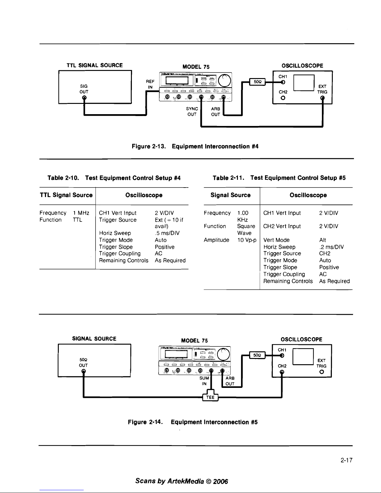
Figure 2-1
3.
Equipment lnterconnection #4
TTL SIGNAL SOURCE
MODEL 75 OSCILLOSCOPE
SIG
OUT
Q
Table 2-10. Test Equipment Control Setup #4 Table 2-1 1. Test Equipment Control Setup #5
Frequency 1 .OO
KHz
Function Square
Wave
Amplitude 1 0 Vp-p
REF
IN
-
TTL Signal Source
Frequency 1 MHz
Function
lTL
Signal Source
CHI Vert Input 2 VIDIV
SYNC
OUT
Oscilloscope
CHI Vert Input 2 VIDIV
Trigger Source Ext (-10 if
avail)
Horiz Sweep
.5
ms1DIV
Trigger Mode
Auto
Trigger Slope
Positive
Trigger Coupling AC
Remaining Controls As Required
Oscilloscope
CH2 Vert Input 2 VIDIV
'rn-mo'
0
0
.
-
-
...
.
OOOOOOOO0
@
L@
@
69
@
..q
ARB
OUT
Vert Mode Alt
Horiz Sweep
.2 ms1DIV
Trigger Source CH2
Trigger Mode Auto
Trigger Slope Positive
Trigger Coupling AC
Remaining Controls As Required
50Q
cl
CH2
,;
-
0
Q
SIGNAL SOURCE MODEL 75 OSCILLOSCOPE
CH2
0
SUM
ARB
IN
OUT
Figure 2-14. Equipment lnterconnection #5
Scans
by
ArtekMedia
O
2006
Page 29

r
WAMTCK:
1
San
Dleao
CA USA
-
I
MODEL
75
I
BEFOREOPENING UNPLUGPOWEO
CORD DANGEROUS
VOLTAGES
INSIDE SEE MANUAL FOO SAFETY
IY9TFtllCTIOII
Z
AXIS
out
IEEE-488
(600nI
Ref Ref
Hold
Return
In
Out
In In
(TTL)
(TTLI (TTL)
(TTL)
Figure
3-1.
Controls, Connectors, and Indicators
Scans
by
ArtekMedia
O
2006
Page 30

3.1 INTRODUC'I'ION
This section describes the operation of the Model 75.
Paragraph 3.2 describes the controls and connectors
of the instrument. The following paragraphs describe
how to use the various features and modes of the Model
75.
3.2 CONTROLS, CONNECTORS, AND INDICATORS
The front panel controls are organized into four menu
selection keys, three soft keys, three real time keys, the
Counter key, and the Control knob. To change any instrument setting, the appropriate menu key is pressed
repeatedly until thedesiredsoft key labelappears in the
bottom line of the display (see Appendix B for menu
organization). Pressing the associated soft key will cause
the top line of the display to indicate the setting to be
changed. Rotating the Control knob will change the
setting. When the setting being changed has the
possibility of irreversibly changing a waveform, an
execute label (EXEC) will appear for the F3 soft key and
must be pressed before the change takes place. The
Trigger, Hold, and Return keys control the waveform in
real time and are not directly associated with the Control knob. The Counter key causes the display to indicate
a waveform count as will be discussed below. The front
panel controls and connectors are shown in figure 3-1
and keyed (bold numbers) to the following descriptions.
W-TEK
Arbitrar, Waveform Generator
FFtEl;!
F;ER
;!;RplFL
1 Liquid Crystal Display
(See figure 3-2). The lower
row of this display will provide labels for the soft keys
that are located directly below the display. Each time
one of the menu keys is pressed the labels will be
updated to match the menu selection (see Appendix B). The upper row of the display will respond to
the soft keys and control knob by indicating the
setting or parameter value corresponding to the last
soft key that was pressed.
2
LCD Viewing Control.
This control allows the user
to adjust the intensity of the display to match the
viewing angle of the instrument.
3 Edit Key.
Each time the edit key is pressed the lower
line of the display will change to indicate three different waveform editing options. There are a total
of five different sets of three editing options. Any of
these can be invoked by pressing the soft key
[Fl
(21), F2 (1
9),
or F3 (1 7)] below the corresponding
label on the display.
NOTE
Refer to appendix B for a summary of soft key
options.
'
WAVETEK
Arbitrary Waveform Generator
L
FREQ SELECTED FROM PARAMETER MENU
ADJX
SELECTED FROM EDIT MENU
Figure 3-2. Typical Display Indications
3-1
Scans
by
ArtekMedia
O
2006
Page 31

Pressing the Edit key the first time enables the rubber
band editing features as follows:
The label for the
F1 soft key will read "CSR" (Cur-
sor). Pressing
F1 allows the cursor in the
waveform to be moved by rotating the control
knob. The top line of the display will indicate the
X-position of the cursor and the Y-value at that
position. If Z-axis modulation is used on an
oscilloscope, the cursor will be intensified. This
does not affect the output waveform.
The label for the F2 soft key will read
"ADJX,Ym
(Adjust X or Y). Pressing F2 once allows a vertex
(at the cursor position) of a waveform to be moved
horizontally (X) by rotating the control knob. Pressing the F2 key twice allows vertical (Y) movement.
The top line of the display will indicate the X and
Y position of the
vertex(cursor) and also(with an
annunciator) the adjustment axis (X or Y) currently
enabled
The label for the F3 soft key will read
"L,R'TT1' (Left
or Right Thumbtack). Pressing F3 once allows the
horizontal position of the left thumbtack to be
changed by rotating the control knob. Pressing
the F3 key twice allows the horizontal position of
the right thumbtack to be changed. The position
of both thumbtacks will be indicated on the top
line of the display along with an annunciator
indicating the thumbtack whose adjustment is
currentlyenabled. If Z-axis modulation is used on
an oscilloscope, the thumbtacks will be
intensified.
Pressing the Edit key the second time enables the
standard waveform features as follows:
The label for the
F1 soft key will read "FUNC"
(Function). Pressing
F1 allows standard waveforms to be inserted between thecurrent thumbtacks (as set by
L,RTT). The desired standard
waveform is selected by rotating the control knob
and is inserted when the EXEC soft key is pressed
as discussed below.
The label for the F2 soft key will read "ERASE"
Pressing this key followed by the EXEC soft key
will erase the entire active waveform by chang-
ing all Y-values to
0.
The label for the F3 soft key will read "EXEC".
(Execute). Pressing F3 causes the action selected
by the FUNC or ERASE keys to be executed. An
"Xu will be be displayed in the top right hand
corner of the display after EXEC has been
pressed.
Pressing the Edit keya third time enables thedigital
amplitude and offset features as follows:
The label for the
F1 soft key will read "DAMPL"
(Digital Amplitude). Pressing
F1 allows adjust-
ment, by rotating the control knob, of the amplitude of the portion of the waveform between the
thumbtacks without affecting the rest of the
waveform. To accomplish this, the Model 75
digitally scales the Y-values of the waveform
points between the thumbtacks. The top line of
the display will indicate the amplitude of the portion being adjusted as a percentage of full scale.
The digital amplitude can be adjusted to a
negative relative amplitude in order to invert a portion of the waveform.
The label for the F2 soft key will read "DOFF"
(Digital Offset). Pressing F2 allows a portion of the
waveform between the thumbtacks to be offset
vertically, by rotating the control knob, without
affecting the rest of the waveform. The Model 75
accomplishes this by adding (or subtracting) a
fixedvalue to all of the points between the thumbtacks.
The range of digital offset adjustment is
limited by the fact that the Y-value of any point
cannot be outside the range of
+
2047, so the
Model 75 will not allow this range to be exceeded.
The top line of the display will indicate the offset,
in points, relative to the original position, of the
portion being adjusted.
The label for the
F3soft keywill read "L,R'TT" (Left
or Right Thumbtack). Pressing
F3once allows the
horizontal position of the left thumbtack to be
changed by rotating the control knob. Pressing
F3 twice allows the horizontal position of the right
thumbtack to be changed. The position of both
thumbtacks will be indicated on the top line of the
display along with an annunciator indicating the
thumbtack whose adjustment is currently
enabled. Moving the thumbtacks has
noeffect on
theoutput waveform. If Z-axis modulation is used
on an oscilloscope, the thumbtacks will be
intensified.
Pressing the Edit key a fourth time enables
startlstop
address control and the waveform normalization
function as follows:
The label for the
F1 soft key will read "START"
(Start Address). Pressing
F1 allows setting, by
rotating the control knob, of the address of the
first waveform memory location to be part of the
active waveform. The top line of the display will
indicate both the current start and stopaddresses
along with an annunciator indicating that START
has been pressed.
The label for the F2 soft key will read "STOP"
(Stop Address). Pressing F2 allows setting, by
rotating the control knob, of the address of the
last waveform memory location to be part of the
Scans
by
ArtekMedia
O
2006
Page 32

active waveform. The top line of the display will
indicate both the current start and stop addresses
along with an annunciator indicating that START
has been pressed.
The label for the F3 soft key will read "NORML"
(Normalize). Pressing the F3 key scales the portion of the waveform between the thumbtacksso
that its peak
Y-value is either k 2047. This is
exactly the same as using DAMPL and turning the
control knob until "1
0O0/0 " isdisplayed. Normalizing a waveform ensures that its peak value will
be as set by the amplitude parameter.
Pressing the Edit keya fifth time enables the single
point editing features as follows:
The label for the
F1 soft keywill read "CSR" (Cur-
sor). Pressing
~1 allows the cursor in the
waveform to be moved by rotating the control
knob. The top line of the display will indicate the
X-position of the cursor and the
Y-value at that
position. If Z-axis modulation is used on an
oscilloscope, the cursor will be intensified. This
does not affect the output waveform.
The label for the F2 soft key will read "INCRX"
(Increment X Position). Pressing F2 causes the
positionof thecursor to increase
byone.The top
line of the display will indicate the X-position of
the cursor and the
Y-value at that position. This
does not affect the output waveform.
The label for the F3 soft key will read "ADJY PT"
(
Adjust the Y-Value of a Point). The level of
individual points of the waveform can be adjusted
by pressing F3 and rotating the control knob. The
top line of the display will indicate both
theX posi-
tion and Y value of the point.
Pressing the Edit key additional times will continuous
cycle through the above options.
4
Parameter Key.
Each time the Parameter key is
pressed the lower line of the display will change to
indicate three different parameter setting options.
There is a total of three different sets of three
parameter setting options. Any of these can be
invoked by pressing the soft key
[Fl (21), F2 (1
9),
or
F3(17)] below the corresponding label on thedisplay.
NOTE
Refer to appendix B for a summary of the soft
key options.
frequency(see paragraph 3.1 4.1), but the display will
be in three different forms as follows:
The label for the
F1 soft key will read "FREQ"
(Waveform Frequency). Pressing
F1 allows the
frequency to be set using the control knob.
The label for the F2 soft key will read "PER"
(Waveform Period). Pressing F2 allows the period
to be set using the control knob.
The label for the F3 soft key will read "SAMPL"
(Sample Frequency). Pressing F3 allows the sample freauency to be set using the control knob.
Pressing the Parameter key a second time enables
amplitude-offset control and also allows the selection of external frequency reference as follows:
The label for the
F1 soft key will read "AMPL"
(Amplitude). Pressing
F1 allows setting of the
peak amplitude by rotating the control knob. The
top line of the display will indicate the amplitude
in volts
peak(into 509). See paragraph 3.1 4.3for
an explanation of the interrelation between
amplitude and offset.
The label for the F2 soft
keywill read "OFFSET".
Pressing F2 allows setting of the output offset
voltage by rotating the control knob. The top line
of the display will indicate the offset in volts (into
509). See paragraph 3.14.4 for an explanation of
the interrelation between amplitude and offset.
The label for the
F3soft keywill read "REF" (Frequency Reference). Pressing F3 allows selection
of either the internal synthesizer (as set by FREQ,
PER, or SAMPL) or an external signal (Ref in
connector-27) by rotating the control knob.
Pressing the Parameter a third time enables the
mode controls as follows:
The label for the F1 soft key will read "MODE".
Pressing
F1 allows'selection of one of the five
operating modes by rotating the control knob.
The label for the F2 soft key will read "TRSLP"
(Trigger Slope). Pressing F2 allows the selection
of the trigger slope polarity as either positive or
negative by rotating the control knob.
The label for the F3 soft key will read "BURST"
(Burst Count). Pressing F3 allows the setting of
the number of waveform cycles to be output after
each trigger in burst mode by rotating the control knob.
Pressing the Parameter key additional times
will con-
tinuously cycle through the above options.
Pressing the Parameter key the first time enables
5
Store Key.
Each time the Store key is pressed the
the control of theoutput frequency in threedifferent lower line of the display will change to indicate one
ways. Each of these is actually settng the sample of two sets of three setting storage options. Setting
Scans
by
ArtekMedia
O
2006
Page 33

storage is only available for waveform lengths of
2048 points or less (see CHAI N below). Any of these
can be invoked by pressing the soft key
[Fl (21), F2
(1
9), or F3(17)] below the corresponding label on the
display.
NOTE
Refer to appendix B for a summary of the soft
key options.
Pressing the Store key the first time enables the store
and recall functions as follows:
The label for the F1 soft key will read "STORE".
Pressing the
F1 key, selecting one of the three
locations with the control knob, then pressing
EXEC key (see F3 below), will copy the current
waveform and settings into the selected location.
The previous contents of the selected location will
be lost.
The label for the F2 soft key will read "RCALL"
(Recall). Pressing the F2 key, selecting
oneof the
three locations with the control knob, then pressing EXEC key (see F3 below), will copy the
selected waveform and setting into the active
instrument setup. The previous setup and waveform will be lost.
The label for the F3 soft key will read "EXEC"
(Execute). Pressing F3 causes the action selected
by the STORE or RCALL keys to be executed. An
"X" will be displayed in the top right hand corner
of the display after EXEC has been pressed.
Pressing the STORE key a second time will enable
the exchange function and the chain option as
follows:
The label for the
F1 soft key will read "EXCHG"
(Exchange). Pressing the
F1 key, selecting one
of the three locations with the control knob, then
pressing EXEC
key(see F3 below), will exchange
the current waveform and settings with the
selected location. In this way, neither waveforms
nor settings are lost.
The label for the F2 soft key will read "CHAIN".
The Chain function allows chaining the active
waveform memory with the three waveform
storage areas to produce waveforms longer than
2048 points. Pressing the F2 key, selecting
"8K"
with the control knob, then pressing EXEC key will
chain the waveforms together. Pressing the F2
key, selecting
"2K" with the control knob, then
pressing "EXEC"
keywill unchain thewaveforms
and
reenable waveform and setting storage.
The label for the F3 soft key will read "EXEC"
(Execute). Pressing F3 causes the action selected
by the EXCHG or CHAIN to be executed. An
"X"
will be displayed in the top right hand corner of
the display after EXEC has been pressed.
Pressing the Store key additional times will continuously cycle through the above options.
6
Setup
Key.
Each time the Setup key is pressed the
lower Iineof
thedisplaywill change to indicate three
different instrument setupoptions. There are a total
of four different sets of three parameter setting
options if no communications option
(RS-2326 or
IEEE-488) is installed or five sets if a communication option is installed. Any of these can be invoked
by pressing the soft key
[Fl (21), F2 (1 9), or F3 (1 7)]
below the corresponding label on the display.
NOTE
.
Refer to appendix B for a summary of the soft
key options.
Pressing the Setup key the first time enables the
sync pulse and ramp rate controls as follows:
The label for the
F1 soft key will read "SYNC".
Pressing
F1 allows the position of the pulse from
the Sync Out connector
(1 3) to by set to anywhere
in the active waveform by rotating the control
knob. The top line of the display will indicate this
position by the waveform address and in degrees
relative to the beginning of the waveform.
The label for the F2 soft key will read "PHASE".
Pressing
F2allows the adjustment of the relative
phase of different model 75s running in parallel
by rotating the control knob. The top line of the
display indicates the phase in degrees relative to
the beginning of the waveform. This actually is
moving the sync pulse just as in SYNC above,
except that there isa two point offset in thedegree
reading on the display.
The label for the F3 soft key will read "RAMP"
(Ramp to Start Rate). This is the rate at which the
output ramps back to the start value when the
"Return" feature is used. Pressing F3 allows this
rate to be set by rotating the control knob.
Pressing the Setup key a second time enables the
break point setting features as follows:
The label for the
F1 soft key will read "CSR" (Cur-
sor). Pressing
F1 allows the cursor in the
waveform to be moved by rotating the control
knob. The top line of the display will indicate the
X-position of the cursor and whether a break point
is ''on'' or "off" at that position.
If
Z-axis modulation is used on an oscilloscope, the cursor will be
intensified. This does not affect the output
waveform.
Scans
by
ArtekMedia
O
2006'
Page 34

The label for the F2 soft key will read "NEXTBP"
(Go to Next Break Point). Pressing F2 will cause
the cursor to jump to the next location where a
break point is "on".
The label for the F3 soft key will read "TGLBP"
(Toggle Break Point
OnIOff). Pressing F3 will turn
a break point "on"
if
it is "off" or "off" if it is "on"
at the current cursor position.
Pressing the Setup keya third time enables the break
point clearing and reset functions as follows:
The label for the
F1 soft keywill read "CLRBPS"
(Clear all Break Points). Pressing
F1, then the
EXEC key, will clear all of the currently set break
points (turn them "off"), and insert the default
break point at the start address.
The label for the F2 soft key will read "RSET"
(Reset). Pressing F2, then the EXEC key, will reset
the instrument to the defaults listed in table
3-1.
This will not affect the active or stored waveforms.
The top line of the display will indicate the software version number.
The label for the F3 soft
keywill read "EXEC" (Execute). Pressing F3 causes the action selected
by the CLRBPS or RSET to be executed. An
"X"
will be displayed in the top right hand corner of
the display after EXEC has been pressed.
Pressing the Setup key a fourth time enables the
Z-axis and calibration controls as follows:
The label for the
F1 soft key will read "ZLEVL"
(Z-Axis Drive Level). Pressing
F1 allows adjust-
ment of the amplitude at the Z-axis output con-
nector (23) by rotating the control knob. The top
line of the display indicates this level in volts. Refer
to paragraph 3.5 for a procedure for setting up
Z-axis modulation.
The label for the F2 soft key will read "ZLOGIC"
(Z-Axis Logic Polarity). Pressing F2 allows setting
of the Z-axis output (23) to either positive
(high =bright) or negative (low
=
bright) by
rotating the control knob. Refer to paragraph 3.5
for a procedure for setting
upz-axis modulation.
The label for the F3 soft key will read
"CAL"
(Calibration). Pressing F3 allows the calibration
of the output offset. Refer to section 5 for the
calibration procedure.
Pressing the Setup key a fifth time enables the
communication option controls if a communication
option is installed. Refer to paragraph 3.26
(IEEE-488) or 3.30 (RS-232-C) for more information
about these controls.
Pressing the Setup key additional times will continuously cycle through the above options.
7
Control Knob. Used to change the value or selection associated with the three soft key. The top line
of the displaywill display
thevalue or selection made
by the control knob.
8
Power Switch.This switch turns the instrument On
or Off. At power-on, the instrument initializes to the
conditions existing when the instrument was last
turned off.
9
ARB Out (50R) Connector. This BNC connector is
the main output for the ARB waveform. The maxi-
mum voltage output amplitude is
+
5 Vp into a 50R
load. This connector is internally fuse protected.
Return Key. Pressing the Return key causes the out-
put to ramp back to the starting
"Y"
value. The rate
of the ramp is adjustable from
0 to 100 ms per
vertical point. If the instrument is in Continuous
mode, the output will be held after the return and can
be restarted by pressing the Hold key. If the
waveform is in the Trigger, Gate, Toggle, or Burst
mode, the output will wait for another trigger (manual
or external) before restarting.
11
Sum in (50R) Connector. Provides a means of
inputting an external waveform to be summed with
the ARB internal waveform. This input is fuse protected against accidental application of high voltage.
A
+
5Vp input will produce an output equal to the
amplitude setting at the "ARB Out" connector. The
sum of this signal and the .internal waveform can-
not exceed
+
5 Vp.
12
Hold Key. This key, when pressed, will stop the
waveform at the ARB Out connector and hold the
output at the instantaneous (when pressed) value
of
"Y".
Pressing the Hold key a second time will con-
tinue the original waveform.
13
Sync Out (TTL) Connector. This connector provides
a sync signal for synchronizing an oscilloscope or
another ARB generator with this ARB generator. The
waveform from this connector is a pulse one Sample time wide. The position is adjustable toanywhere
in the waveform.
14
Trigger Key. This key allows the waveform to be
manually controlled in four different ways depending
on the mode. The trigger slope polarity (TRSLP) is
settable as either positive or negative.
1. When in the Triggered Mode the generator will
output one cycle of the waveform each time the
key is pressed.
Scans
by
ArtekMedia
O
2006
Page 35

2. When in the Gated Mode the generator will
output a continuous waveform as long as the
key is pressed. When the key is released the
waveform will cease.
3. When in
theToggle Mode, pressing the key once
will output a continuous waveform. Pressing
the key a second time will stop the waveform
output.
4 When in the Burst Mode, the generator
w~ll
output the preset number of cycles.
15 Counter Key. When in the Gated, Toggled, or Burst
Modes pressing this key will indicate the number of
complete cycles of the waveform that have been output since the last trigger.
16 Sync In (TTL) Connector. Primarily used for
synchronizing several arbitrary waveform
generators in parallel. A high level at this input
causes the waveform to restart operation at the start
address.
17 F3
Key.This is a soft key that allows selection of the
option displayed directlyabove it. The function of this
key ischanged
bythe menu keys(3.4.5. and 6) The
top
l~ne of the display will respond to the key being
pressed
For some menus, the F3 soft key
(1
7)
will have an
"EXEC" label. Pressing the F3 soft key will cause
the condition or value set by the
F1 or F2 soft key
to be entered (executed).
18 Burst Done Out
(TTL)Connector. This output is low
during active waveform output and high while
waiting for a trigger in Trig, Gate, Toggle, and Burst
modes. It is primarily used as the trigger source to
start another ARB generator in series operation.
19 F2
Key.This isa soft key that allows selection of the
option displayed directlyabove
it.Thefunction of this
key is changed by the menu
keys(3,4,5, and 6). The
top line of the display will respond to this key being
pressed.
20 Trig
In(TTL)Connector.This connector provides for
an external
lTL signal input to control the generator
in the Trigger, Gate, Toggle, and Burst modes. The
slope polarity (TRSLP) is settable.
21
F1 Key.This is a soft key that allows selection of the
option displayed directly above it. The function of this
key is changed by the menu keys
(3,4,5, and
6).
The
top line of the display will respond to this key being
pressed.
22 Communication Option Connector. Either an
IEEE-488 connector, an
RS-232C connector, or a
blank cover plate will be mounted here depending
on the option installed.
23 Z-Axis Out
(600R)Connector. Used to modulate the
Z-axis of an oscilloscope when using the waveform
editing features. The level of
th~s signal is menu
selectable from 2 to 14 volts. Additional lower levels
can be obtained by terminating the output into
50R.
Logic polarity is also selectable.
24 Return In (TTL) Connector. A
lTL low or switch
closure applied at this input will cause the output to
ramp back to the starting
"Y"
value. The rate of the
ramp is adjustable from
0 to 100 ms per point. If the
instrument is
incontinuous mode, the output will be
held after the return and can be restarted by pressing the hold key.
If
the waveform is in Trig, Gate,
Toggle, or Burst, the output will wait for another
trigger (manual or external) before restarting.
25 Hold In (TTL) Connector.
AlTL low or switch closure
signal at this input will cause the waveform to stop
at the instantaneous
"Y"
value. ATTL high or open
will cause the waveform to continue.
26 Ref
Out(TTL) Connector. This connector outputs a
lTL level pulse train at the sample frequency to synchronize other ARB generators in series or parallel
operation.
27 Ref In
(T'TL) Connector. This connector allows the
input of an external
lTL level sample clock when
external reference is selected.
28 External Power Connector. This connector allows
the use of a standard 3-wire, UL
IistedlCSA certified,
removable power cord.
NOTE
All outputs that are specified as
"TTL"
are defined as
follows:
HIGH Vout 24.4V @ lout G20 pa
Vout 23.8V @ lout G4 ma
LOW
Vout GO.l V @ lout G20 pa
VoutG0.33V @ lout <4 ma
Scans
by
Artekhledia O 2006
Page 36

Beforesetting up the instrument, the instrument can be
RECEIVING
MODEL
75
cleared (reset) to the default settings listed in table 3-1
INSTRUMENT
by using the RSET soft key from the Setup menu. RSET
OUTPUT
RG58
OR
EFFECTIVE
will not affect calibration, Z-axis output, or any
IMPEDANCE
EQUIVALENT CIRCUIT
waveforms. To clear the old waveform, in order create
RESISTANCE
~OQ
a new one, the ERASE soft key from the Edit menu can
LOAD
be used. Resetting, then erasing, is normally the best
way to start a new test setup. To use the RSET soft key,
press the Setup key repeatedly until the RSET label is
OUTPUT
AMPLIFIER
seen on the bottom line of the display and then press the
v
RSET soft key (F2) followed by the EXEC soft key (F3).
Table 3-1. Model 75 Default Conditions
Figure 3-3. Signal Termination
-
3.3 OPERATION
The following paragraphs describe the various operational configurations and features of the Model 75.
Descriptions of the individual controls and connectors
may be found in paragraph 3.2.
Proper signal termination, or
loadiog, of the ARBOut con-
nector is necessary for its specified operation. Figure
3-3 shows the proper termination of the ARB Out con-
nector with standard 509 output impedance. Placing the
50
9
terminator, or 509 resistance, in parallel with a
higher load impedance, matches the receiving instrument input impedance to the coax characteristic and
generator output impedance, thereby minimizing signal
reflection or power loss on the line due to impedance
mismatch.
The impedances of the generator input and output con-
nectors are:
Connectors Impedance
ARB Out (509).
.........................
,509
Sync Out (lTL).
.........................
NIA
Burst Done Out (lTL).
.....................
NIA
Ref Out (lTL)
......................
NIA
Z-Axis Out (6009).
.................
,6009
Sum In (509).
.........................
,509
Trig In (lTL).
.........................
.1OOkR
Sync In (lTL)
..........................
.100kR
Ref In (lTL)
..........................
.100kR
Hold In (lTL).
.......................
,100kR
Return In (lTL).
.......................
.look9
3.4 INITIAL SETUP
When power is turned on, Model 75 will assume the instrument setup conditions that were present when power
was last turned off. If, when power is first turned on, the
bottom line of the display reads "**COLD START**",
memory has been lost due to a low battery and the
instrument will need to be calibrated and set up again.
Sample Frequency: 1.0000 MHz
Frequency: 488.28 Hz
Period: 2.0480 ms
Amplitude: 5.000 Vp
Offset:
O.OOV
Reference: Internal
Mode: Continuous
Trigger Slope: Positive
Burst: 8
Cursor: X
=
1023
Left Thumbtack: 0000
Right Thumbtack: 2047
Function: DC
Start Address: 0000
Stop Address: 2047
Sync Address: 0000 0.00"
Phase Difference: 0.35"
Ramp Time: 5
mslbit
Z Level: (Not Affected)
Z Logic: (Not Affected)
Chain: 2K
Hold: Off
3.5 EDITING WAVEFORMS
Waveform editing is best accomplished using an
oscilloscope with Z-axis modulation to emphasize the
"thumbtacks" and "cursor" used by the editing
features. Oscilloscope Z-axis inputs vary widely in maximum input voltage and polarity. Consult your
oscilloscope manual for the limits and then use the
following procedure.
1. Setting the Z-axis logic polarity.
a. If a high level reduces the intensity of your
oscilloscope, then set the "ZLOGIC" polarity to
"NEG"
usiog the ZLOGIC soft key (from the
Setup menu) and the Control knob.
b.
If
a high level increases the intensity of your
oscilloscope, then set the "ZLOGIC" polarity to
"POS" using the ZLOGIC soft key (from the
Setup menu) and the Control knob.
Scans
by
ArtekMedia
O
2006
Page 37

2. Setting the Z-axis voltage level.
The Z-axis output has a fixed low level of approxi-
mately 0.2 volts and a high level that is adjustable
to approximately
2,4,6,8,10,12, or 14 volts. If your
oscilloscope can be damaged by any of these Z-axis
output levels, be sure that you do not exceed the
maximum for your oscilloscope. This output can be
loaded with a 50Q feedthrough termination to reduce
these levels by approximately a factor of 10.
Set the
timebase on the oscilloscope to show one
or more waveform periods, then use the following
procedure to adjust the Z-axis output and
oscilloscope intensity for best viewing.
a. With no feedthrough termination, set the Z-axis
level to 2 volts using the ZLEVL soft key (from
the Setup menu). Connect the Z-axisoutput
cable to the oscilloscope.
b. Adjust the oscilloscope intensity to the desired
brightness.
c. If the contrast between the bright dots (thumb-
tacks and cursor) and the rest of the waveform
is too high, add a 50R feedthrough termination
and return to step b. Alternately adjust the
ZLEVL and oscilloscope intensity until the
brightness and contrast are as desired.
3.6 THUMBTACKS AND CURSOR
Most of the waveform editing features use "thumbtacks"
for defining the portion of the waveform to be edited. The
thumbtacks are marked by pulses on the Z-axis output
and therefore show up as bright dots on an oscilloscope
waveform if Z-axis modulation is used. The position of
the thumbtacks is adjusted by using the
L,RTT soft key
from the Edit menu. Pressing this soft key the first time
enables adjustment of the left thumbtack (lower address)
with the Control knob. Pressing the soft key additional
times alternates between enabling adjustment of the
right thumbtack and the left thumbtack. Acursor is used
for "point" and "rubber band" editing. The position of
the cursor can be adjusted by selecting the CSR soft key
(from the Edit menu). The cursor
isalso marked bya pulse
on the Z-axis output and will show up as a bright dot on
the oscilloscooe display.
3.7 RUBBER BAND EDITING
"Rubber band" editing is analogous to stretching a
rubber band fromone thumbtack, to the cursor, and then
to a second thumbtack. To use this editing method, place
the left and right thumbtackson each side of the portion
of the waveform to be edited (use
L,RTT), then use the
ADJX,Y soft key and Control knob to move the vertex
either in the X (horizontal) or Y (vertical) direction. The
CSR soft key can be used to pre-position the cursor
(without changing the waveform) before using the
ADJX,Y function. This is useful for editing the waveform
while the Model 75 is connected to a system under test.
3-8
3.8 INSERTING STANDARD WAVEFORMS
Standard waveforms (sine, cosine, haversine, inverse
sine, triangle, square, ramp up, ramp down, dc) are
inserted between the thumbtacks using the FUNC soft
key (from the Edit menu). When a standard waveform
is inserted, it will be at full amplitude (as set by AMPL
parameter) and centered around the offset voltage (as
set by the OFFSET parameter). The relative amplitude
and offset can be adjusted using "DAMPL" and "DOFF"
as described in paragraphs 3.9 and 3.1 1. To insert a
standard waveform:
1. Set the desired end points using the
L,RTT soft key
(from the Edit menu).
2.
Press the FUNC soft key (from the Edit menu) and
use the Control knob to select thedesired waveform
3. Press the EXEC soft key to insert the waveform.
4. Use "DAMPL" and "DOFF" as described in
paragraphs 3.9 and 3.1 1 to change the relative
amplitude and offset of the inserted waveform if
necessary.
3.9 DIGITAL AMPLITUDE
The "Digital Amplitude" editing feature allows adjustment of the amplitude of a portion of the waveform
relative to the rest of the waveform. The waveform
consistsof a 4095point high windowwith anamplitude controlled by the "AMPL" parameter. The "DAMPL" editing
feature adjusts the amplitude of a portion of the
waveform relative to this window. The change in
amplitude is referenced to the left thumbtack as the zero
point. The digital amplitude feature is not available in
chained operation (waveforms longer than 2048 horizontal points). To use digital amplitude, set the end points
of the section to be edited using the
L,RTTsoft key(from
the Edit menu), press the DAMPLsoft key, and then use
the Control knob to adjust the amplitude. The digital
amplitude can be adjusted past zero to negative
amplitude to invert a portion of the waveform.
3.1 0 NORMALIZING
Pressing the "NORML" soft key from the "EDIT" menu,
scales the portion of the waveform between the thumbtacks such that the peak value will be
+
2047 or - 2047
points. This is equivalent to adjusting the digital
amplitude to full scale.
3.1 1 DIGITAL OFFSET
"Digital Offset" is similar todigital amplitude, but is used
to adjust the offset of a portion of the waveform relative
to the rest of the waveform. To use digital offset, set the
left and right thumbtacks
(L,RTT soft key from the Edit
menu) to the ends of the portion to be offset, press the
DOFF soft key, and then use the Control knob to adjust
the offset. When adjusting the digital offset, the Z-axis
output is turned off
toenable more accurate adjustment
when viewing on an oscilloscope.
Scans
by
ArtekMedia
O
2006
Page 38

3.12
POINT EDITING
"Point" editing is used to edit individual points in a
waveform. To edit individual points, press the Edit menu
key repeatedly until "CSR INCRXADJYPT" appears on
the bottom line of the display. Press the CSR soft
key(F1)
and use the Control knob to move the cursor to the first
point to be edited. Press the ADJYPT soft key (F3) and
use the Control knob to adjust the
"Y" value of the point.
Pressing the INCRX soft
key(F3)wiII increment the "X"
value by
1,
pressing ADJYPTa second time will re-enable
adjustment of this next point. In this way successive
points of the waveform can be edited by repeatedly
pressing the INCRX, then ADJYPT soft keys and rotating
the Control knob.
Example
Setup
The following procedure produces a simulated medical
"EKG" waveform.
1. Connect the equipment (Model 75 and the
oscilloscope) as shown in the diagram.
Z-AXIS
a. "ARBOut (504)" through a 504feedthrough ter-
mination to the vertical input of an oscilloscope.
b. "Sync Out
(TTL)" to the external trigger input
of the oscilloscope.
c. "Z-Axis Out
(600R)" to the Z-axis input of the
oscilloscope. Use procedure in paragraph 3.5
to set the Z-axis intensity.
Set the Model 75 and oscilloscope controls as
follows:
Model
75
Oscilloscope
Setup: Press 3 times
VERT INPUT: 2
VlDlV
F2 (RSET): Press once VERT COUPLIIVG: DC
F3 (EXEC): Press once
Edit: Press two times
HORlZ SWEEP:
F2 (ERASE): Press once
.2 mslDIV.
F3 (EXEC): Press once
TRIG MODE: AUTO
TRlG
COUPI-ING: AC
TRlG SOURCE:
EXTI1 0
TRIG SLOPEILEVEL: As Required
INTENSITY: As Required
by paragraph 3.5
3. The oscilloscope will now display a dc waveform of
OV with a left and right thumbtack and a cursor in
the center as shown below.
4.
Some oscilloscope controls(depending on the make
and model of oscilloscope used) may need to be
adjusted slightly from the positions given in step 2.
a. Adjust the oscilloscope horizontal trace (posi-
tion control) to place the left thumbtack (inten-
sity
marker)at the left-hand edge vertical mark.
b. Adjust the oscilloscope horizontal
"VAR" con-
trol to place the right thumbtackat the right-hand
edge vertical mark. One complete waveform
cycle will then equal 10 divisions on the
oscilloscope screen.
5. Edit:
F3
(L,RTT):
Control Knob:
F3
(L,RTT):
Control Knob:
Edit:
F1 (FUNC):
Control Knob:
F3 (EXEC):
Press four times
Press once
Rotate CW until the display
indicates
">
L = 0720"
Press once
Rotate CCW until the display
indicates
">
R = 1325"
Press once
Press once
Rotate CW until the display
indicates "FUNC COSINE"
Press once
Scans
by
ArtekMedia
O
2006
Page 39

6.
Edit: Press once.
F1 (DAMPL): Press once.
Control Knob:
Rotate CCW until the display
indicates "DIG AMPL
50%"
F2 (DOFF): Press once
Control Knob:
Rotate CCW until the display
indicates "DIG OFFSET
-
2047"
7. F3 (L,RTT): Press once
Control Knob:
Rotate CW until the display
indicates
">
L = 0835"
F3 (L,RTT): Press once
Control Knob:
Rotate CCW until the display
indicates
">
R = 1235"
Edit: Press three (3) times
F2
(ADJX,Y):
Press two
(2)
times
Control Knob:
Rotate CW until the display
indicates
">
Y = 2047"
8.
F3 (L,RTT):
Control Knob:
F3
(L,RTT):
Control Knob:
Edit:
F1 (FUNC):
Control Knob:
F3 (EXEC):
Press once
Rotate CCW until the display
indicates
">
L = 0410"
Press once
Rotate CCW until the display
indicates
">
R = 0730"
Press once
Press once
Rotate CW until the display
indicates "FUNC HAVER
SINE"
Press once
9.
Edit: Press once
F1 (DAMPL): Press once
Control Knob:
Rotate CCW until the display
indicates "DIG AMPL
5%"
F2 (DOFF): Press once
Control Knob:
Rotate CW until the display
indicates "DIG OFFSET
2048"
Scans
by
ArtekMedia
O
2006'
Page 40

F3 (L,RlT):
Press two (2) times 12. Set the oscilloscope horizontal sweep to
.5
mslDIV.
Control Knob:
Rotate CW until the display
Adjust the horizontal sweep "VAR" control until the
indicates
">
R = 1680"
oscilloscope displays four (4) complete cycles of the
F3
(L,RlT): Press once waveform.
Control Knob:
Rotate CW until the display
indicates
">
L = 131 0"
Edit: Press four (4) times
F1 (FUNC): Press once
F3 (EXEC): Press once
11. Edit: Press once
F1 (DAMPL): Press once
Control Knob:
Rotate CCW until the display
indicates "DIG AMPL
6O/0"
F2 (DOFF): Press once
Control Knob: Rotate CW until the display
indicates "DIG OFFSET
2048"
3.1 3
START AND STOP ADDRESSES
The "X" values at the beginning and end of the output
waveform can be set to any value between
0 and 2047
points (81 91 in chained operation) as long as the end is
greater than the beginning. To set the beginning or end,
press START or STOP (from the Edit menu) as desired
and then use the Control knob to set the value. Break
points after the stop address may be lost when moving
the stop address.
3.14
WAVEFORM PARAMETERS
The "Parameter" menu allows changing of the frequency, amplitude, offset, and operational modes. The
following four paragraphs will discuss the frequency,
amplitude, and offset parameters. The operational
modes will bediscussed in paragraphs 3.1
5
thru 3.1
5.5.
3.1 4.1
Waveform Frequency, Period, and Sample
Frequency
The waveform "frequency" can be set from the
Parameter menu in one of three ways; in terms of "fre-
quency'' using the FREQ soft
key(F1), in terms of "time
period" using the PER soft
key(F2), or in terms of "sam-
ple frequency" using the SAMPL soft
key(F3). Adjusting
any of these parameters is actually adjusting the "sample frequency", but the display is calibrated differently
for each soft key. The waveform "frequency" is "sample frequency" divided by the number of horizontal
"points" in the waveform. The waveform "period" is the
inverse of the waveform "frequency". The number of
points in the waveform is thestopaddress minus
thestart
address plus one. To adjust any of these values, press
the associated soft key and then use the Control knob
to set the value.
Scans
by
ArtekMedia
O
2006
Page 41

3.1 4.2 External Reference
An external "clock" signal can be used as the main
"sample frequency" by pressing the REF soft
key(from
the Parameter menu) and using the Control knob to
select "REF EXTERNAL". The external clock signal is
connected to the "Ref In'' connector on the rear panel.
3.1 4.3 Waveform Amplitude
The waveform "amplitude" is displayed in volts peak.
This amplitude is measured from the center of the
waveform window (Y
=
0) to the top or bottom of the
waveform window (Y
=
+
2047). To set the amplitude,
press the AMPL soft key (from the Parameter menu) and
turn the Control knob as required. If the waveform does
not reach the top or the bottom of the window the
indicated amplitude will not be
[he actual amplitude of
the output. The Normalize editing feature can be used
to scale the waveform to match the amplitude setting.
Move the thumbtacks to each end of the waveform and
press the "NORML" soft key (from the Edit menu). The
sum of the amplitude and offset settings automatically
determines the best output attenuator range and
therefore the offset setting will affect the resolution of
the amplitude setting. The sum of the amplitude setting
and the absolute value of the offset setting cannot
exceed
5.2V.
3.1 4.4 Waveform Offset
The waveform "offset" is the voltage from zero to the
center of the waveform window (Y
=
0). To set the
waveform offset, press the OFFSET soft key (from the
Parameter menu) and use the Control knob to set the
desired value. The sum of the amplitude and offset
settings automatically determines the best output
attenuator range and therefore the amplitude setting will
affect the resolutionof theoffset
setting.Thesum of the
amplitude setting and the absolute value of the offset
setting cannot exceed
5.2V.
3.1 5 OPERATIONAL MODES
The Model 75 can operate in any one of five different
modes. These are Continuous, Triggered, Gated,
Toggled, or Burst. Adescription of each of these modes
isgiven in paragraphs 3.1 5.1 thru 3.15.5.Tochange the
operational mode, press the MODE soft key (from the
Parameter
menu)and use thecontrol knob to select the
desired mode.
All of the modes except Continuous use a trigger to start
the waveform output. The trigger
cancome from theTrig-
ger key on the front panel, from the "Trig In" BNC con-
nector on the front
panel,or via the optional GPlB or
RS-232C interface. The polarity(s1ope) that causes the
waveform to run can be set to either positive of negative
by pressing the TRSLP soft key (from the Parameter
menu) and turning the Control knob. When the trigger
slope is set to positive, pressing the Trigger key or
inputting a rising edge on the "Trig In'' BNC will start the
waveform. When the trigger slope is set to negative,
releasing the Trigger key or inputting a falling edge on
the "Trig In" BNC will start the waveform. If the "Trig
In" BNC is held high, the polarity of the Trigger key will
be reversed.
In all modes except Continuous, the waveform will stop
and wait for another trigger only at the break points. By
default, one break point is set at the beginning of the
waveform. Break points can be set anywhere in the
waveform or the default break point can be removed if
desired. Setting and clearing break points will be discussed later.
NOTE
Ifallof the breakpointsare removedfrom the
waveform, then all of the modes will act like
the Continuous mode.
3.1 5.1 Continuous Mode
In Continuous mode, the output runs repeatedly from the
start address to the stop address. Neither the Trigger
key or the "Trig In''
BNCwill have any effect in this mode.
3.1 5.2 Triggered Mode
In the Triggered mode, the waveform stops at a break-
point and waits for a trigger from either the Trigger key
or the "Trig In" input. When a trigger is received, the
waveform runs until another break point is encountered,
then stops and waits for another trigger. With only the
default break point in the waveform, each trigger
produces one waveform cycle.
3.1 5.3 Gated Mode
In the Gated mode, the waveform stops at a break point
and
waitsfor a trigger signal. When a trigger is received,
the waveform runs until the trigger signal is removed and
then stops at the next break point. If the trigger slope
is set to negative, the waveform will start when the Trigger key is released or the "Trig In'' input sees a high to
low transition and runs until the Trigger key is pressed
or the "Trig In" input goes high.
3.1 5.4 Toggled Mode
In the Toggled mode, the waveform stops at a break point
and waits for a trigger signal. When a trigger is received,
thewaveform runs until asecond trigger is received, then
stops at the next break point. In this way, each trigger
toggles the waveform "on" or "off".
Scans
by
ArtekMedia
O
2006
Page 42

3.15.5 Burst Mode
In the Burst mode, a trigger signal causes the generator
to output a predetermined number of waveforms (as set
by the burst count) and stop at the next break point. To
set the burst count, press the
BURSTsoft key(from the
Parameter menu) and use the Control knob to set a count
from 1 to 1,048,575. Inputting another trigger signal during the burst sequence will cause the burst counter to
start over.
3.1
6
SETTING AND CLEARING BREAK POINTS
To insert a "break point" into the waveform, press the
CSR soft key (from the Setup menu) and then use the
Control knob to position the cursor to the desired location in the waveform. The cursor position will be indicated
numerically on the display and as a bright dot on a
oscilloscope if the Z-axis modulation is used. Next,
pcess
the TGLBP soft key (from the Setup menu) to toggle the
break point on. To remove a break point, move the cursor to the location of the break point either with the CSR
soft key and the Control knob or by using the NEXTBP
soft key. The NEXTBP soft key rnoves the cursor to the
next break point. If there is a break point at the present
cursor position, thedisplay will indicate it with the word
"ON" after the cursor address. All of the break points
can be cleared and the default break point (X
=
0000)
inserted by pressing
theCLRBPSsoft key(from thesetup
menu) followed by the EXEC soft key. For the operational
modes to work correctly there must be at least one break
point somewhere in the waveform. TGLBP both sets and
clears breakpoints.
3.1 7 SYNC ADDRESS AND PHASE
Pressing the SYNC soft key (from the Set Up menu)
allows the position of the pulse at the "Sync Out" output to be moved, anywhere relative to the waveform, by
turning the Control knob. The display indicates the
address and phase of the pulse. The PHASE soft key also
allows the adjustment of the sync pulse, but the display
indicates a phase that is offset by two sample times. This
is used to adjust the relative phase of multiple instru-
ments as discussed below under parallel operation.
3.18 STORING AND RECALLING WAVEFORMS
The Model 75 can hold three waveforms in storage in
addition to the
active..waveform. Each of these
waveforms can be up to 2048 samples long. To store a
waveform, press the STORE soft key (from the Store
menu), use the Control knob to choose the storage location, and then press the EXEC soft key to store. Recalling a waveform is done in the same way by using the
RCALLsoft key(from the Store menu). Storing or recalling a waveform erases either the stored waveform or the
active waveform respectively. The EXCHG soft key (from
the Store menu) can be used to exchange two waveforms
without losing either one. Use the EXCHG soft key in the
same manner as the STORE and RCALL soft keys.
3.1 9 CHAINED OPERATION
The "active" waveform can be chained with the three
stored waveforms to create waveforms of up to 81 92
samples long. When set for chained operation the entire
waveform memory is active and no waveform storage
locations are available. Also, the digital amplitude editing
feature is not available. To set the instrument for chained
operation, press the CHAIN soft key (from the Store
menu), rotate the Control knob until "CHAIN
8K" is
shown on the top line of the display, and then press the
EXEC soft key. To set the instrument back to normal
operation, perform the previous operation except rotate
the Control knob to "CHAIN
2K". Chained operation can
also be used to view the "active" waveform and the three
stored waveforms in succession on an oscilloscope.
3.20 WAVEFORM COLINTER
Pressing the Counter key will cause the display to indicate a count of the number of waveforms that have been
completed since the last trigger (up to a maximum of
1,048,575 waveforms). In Continuous and Triggered
modes the counter is disabled. The counter can be read
while the waveform is running or while the waveform is
stopped such as after a gated or toggled sequence. In
this way the length (in
waveforms)of the last toggled or
gated sequence can be displayed.
3.21 WAVEFORM HOLD
The output waveform can be held at its current level by
using either the rear panel "Hold In" BNC or the front
panel Hold key. Each time the Hold key is pressed the
hold function is toggled on or off as indicated on the
display.
AlTL low level or a contact closure on the "Hold
In" BNC holds the waveform and a high or open lets it
run if the front panel Hold key is off.
3.22 RETURN TO START
Pressing the Return key on the front panel or a high to
low transition (or switch closure) on the rear panel
"Return In'' BNC will cause the output to ramp from the
current output level to the level at the start
address.-The
rate of this ramp is adjustable from 0 to 100 ms per
vertical step.
0 is a special case and causes the output
to jump back to the start address level. To set the ramp
rate, press the RAMP soft key (from the Setup menu) and
use the knob to adjust it. In Continuous mode the hold
will automatically be turned on at the end of the ramp
and will need to be turned off with the Hold key to restart
/
Scans
by
ArtekMe
dia
0
2006
Page 43

the waveform output. In all other modes the generator
will be waiting for a trigger after the ramp to restart the
waveform output.
3.23 LOW BATTERY INDICATOR
If
the internal lithium battery runs low, the top line of the
display will display "BAT" in addition to the normal
message when a menu key is pressed. The low battery
will not effect normal operation as long as the power is
not turned off. If the power is turned off the instrument
could lose all of the stored waveforms, setup information and calibration constant. If, when the power is first
turned on, the bottom
lineof the display reads "**COLD
START*
*",
all of the memory has been lost due to a low
battery and the instrument will need to be calibrated and
set up again.
3.24 SERIES OPERATION
Several Model 75's can be connected in series (as shown
in the following diagram), each one generating one or
a burst of waveforms (see figure 3-4) and then triggering the next Model 75 in the chain. The outputs can be
added together using the "Sum In" inputs to produce
one waveform that is a chain of each of the individual
waveforms in succession. This configuration can be used to create waveforms longer than the
81
92
sample
maximum or to create a series of normal waveforms
followed by one or more abnormal waveforms.
MODEL
75
#I
w-.
1
---
.-
---
/
I
@@Pop,
OSClLLOSCOPE
I
BURST DONE
OUT
CH
2
IN
MODEL
75
#2
0
@
-
-
r- = r
-
BURST
b
TRIG IN DONE ARB OUT
OUT
L
SUM IN
first. The "ARB Out" connector of each instrument is
connected to its successor's "Sum In" connector and
the last "ARB Out" connector is used as the main output. Each of the Model 75's can have independent
waveform sample frequencies if desired, but if this is not
necessary, one should be used as the master frequency
reference.
Todo this, connect the "Ref Out" connector
of the master frequency reference to the "Ref In" con-
nector of all of the other Model 75's and set them for
external reference. By doing this, the one sample time
jitter between successive waveforms is eliminated.
MODEL
75
#2
Figure 3-4. Example of Series Waveform
Each Model 75 should be set to either triggered(if it will
be outputting one period of its waveform) or burst mode
if it will be outputting a sequence of waveforms. The
amplitude control of each Model 75 controls not only its
own amplitude but the amplitudeof theoutput due to the
"Sum In" signal. A
k
5V signal at the "Sum In" input
produces an output equal to the amplitude setting. To
maintain linearity, the sum of the internal waveform and
the "Sum In" waveform should not exceed the amplitude
setting. In equation form:
where
W
is the internal digital data
(Y)
value and S is the
voltage at the "Sum In" input at any time. Because of
this, attention needs to be given to the output voltage
at the break point location at the end of each waveform.
Toconnect several Model 75's in series, the "Burst Done
3.25 PARALLEL OPERATION
Out" connector of each Model 75 is connected to its
Several Model 75's can be connected in parallel (as
successor's "Trig In". If the waveform is to run con-
shown in the following diagram) to produce simultaneous
tinuously, the last Model 75's "Burst
DoneOut" connec-
waveforms (see figure 3-5) with a controllable phase
tor is connected back to the "Trig In'' connector of the
relationship.
Scans
by
Artekhledia
O
2006
Page 44

To connect Model 75's in parallel, chose one as the frequency master and connect its "Ref Out" to the "Ref
In" inputs of the other Model 75's. The master should
be set to internal reference and the others set to exter-
nal reference. Starting with the master unit, the "Sync
Out" output of each unit should be connected to the
"Sync In" input of its successor.
000Q
L
0
$J
OSCILLOSCOPE
SYNC
ARB
OUT OUT
I
TRIG IN
REF IN MODEL
75
;7piLv
--
07
I
1
1
ARB
OQ.aq@?q-
OUT
Figure 3-5. Example of Parallel Waveform
--
SYNC IN
After initial setup and after any sync position change,
each instrument must output a sync pulse before all of
the phases will be synchronized.
If
the test setup uses
a mode other than continuous, the outputs should be
disconnected, and the Model 75's run momentarily in
continuous mode to resynchronize the phase after a
phase change.
--
SYNC OUT
3.26 GPIB CONTROLS (Option
001
Only)
The following paragraphs are keyed to controls in figure
3-6.
3.26.1 GPIB Address DIP Switches (6)
At power on, the bit address DIP switch (located on a
PC Board under the top cover) selects the GPIB default
ADRS(address)value. This valuemay be changed from
the front panel. At power off the address returns to the
bit switch setting. See paragraph 2.2.6 bit switch
settings.
3.26.2 Setup Menu Key (4)
Pressing this key five times enables the GPlB com-
munication soft keys described below. The bottom line
of the display will then show the labels for these soft keys.
3.26.3 BUFFR Soft Key (3)
For remotely operated units the BUFFR soft key (from
the SETUP menu) will display the last
16 ASCll
characters received by the GPlB interface. Rotating the
Control knob will scroll through the last 80
ASCll
characters received by theGPIB interface.Thisfeature
can be used as a debugging tool for remote instrument
programming.
3.26.4 ADRS Soft Key (2)
Pressing this key (from the SETUP menu) allows the user
to manually set the GPlB address to some value other
than that set by the internal DIP switches.
The position of the "Sync Out" pulse from one Model
75 controls the phase of the following Model 75. There
are two ways of adjusting the position of the "Sync Out"
pulse. One is to use the "SYNC" soft key from the "Set
Up" menu to adjust the position by the actual address
or phase of the pulse itself. The other is to use the
"PHASE" soft key from the Set Up menu to adjust the
phase relationship of the successive Model 75's in
degrees. Thedifference between the two soft keys
isdue
to the fact that there is a two clock cycle phase delay
from a pulse in at the "Sync In" input to the start address
output level at the output.
3.26.5 LOCAL Soft Key (I)
Pressing this key (from the SETUP menu) brings the
Model 75 into local control providing the controller has
not locked out the key (see paragraph 3.28.1).
3.26.6 Control Knob (5)
Allows the user to scroll through the ASCII characters
received on the GPIB bus when the BUFFR soft key has
been pressed or to set
theGPIBaddress when the ADRS
soft key is pressed.
Scans
by
ArtekMedia
O
2006
Page 45

@
Paragraph
3.26.1
Figure
3-6.
GPlB Controls and Switches
3.27
GENERAL PURPOSE INTERFACE BUS (GPIB)
Paragraphs 3.27 through 3.27.9are provided for readers
who wish further background information on the General
Purpose Interface Bus (GPIB). For specific Model 75 pro-
gramming information, refer to paragraph 3.28 through
3.29.3.
The GPlB interface is an implementation of IEEE
specification 488-1 978. It supports the following interface functions which are described in detail in the
specification. Relevant aspects of these functions are
discussed in following paragraphs.
SHI Complete source handshake.
AH 1 Complete acceptor handshake.
T6 Basic talker.
TEO No extended talker.
L4 Basic listener.
SR1 Complete service request (software
select).
RLI Remotellocal and local lockout.
PPO No parallel poll capability.
DC1 Complete device clearlselective device
clear.
DT1 Complete device trigger capability.
El Open collector drivers.
Instruments on the bus may have "talk" and "listen"
capabilities. The talk capability allows a device to send
data(such aserror message readings)out over the bus.
The listen capability allows a device to receive data (such
as device programming information) from the bus.
The
GPlB consists of 16 negative true signal lines as
shown in figure
3-7. These 16 lines include 8 bidirectional
data lines, 3 handshake lines and 5 control lines. All
devices on the bus interface to these lines with passive
pull up and active pull down. Thus, any device may
"assert" a line by pulling it down to the logic low, or
"true" state.
If
nodevice is asserting the line, it is pulled
up to the logic high, or "false" state. (Only the controller
is allowed to assert certain lines.)
As shown in figure 3-7, devices connected to the bus may
be a LISTENER (only), TALKER (only),
LISTENER1
TALKER or CONTROLLER. The Model 75 is both a talker
and a listener. More than one controller may be con-
nected to the bus, but only one controller may be hard
wired as SYSTEM CONTROLLER, and only one controller
at a time may assume the role of ACTIVE CONTROLLER.
Scans
by
Artekhfedia
O
2006
Page 46

CONTROLLER
'ii&NS'.lI-S Ah3 SECEVES
DATA AN3 MAhAGES '*E
BUS
TALKERILISTENER
TRANSMITS OR
RECEIVES DATA
ONLY RECEIVES DATA
INTERFACE
MAFiAGEMENT
ONLV TRANShllTS DATA
A-h
SRO
REFi
Figure
3-7.
GPlB
Structure
REN
(ATN false) or a command (ATN true).
Whenever ATN is set true, no activity is
allowed on the bus except for controller
originated messages.
The Remote Enable line controls whether
devices on the GPlB are in local or
remote modes. In the local mode,
devices respond to front panel
commands. In remote mode, the situation is reversed; GPlB originated commands are obeyed, while front panel
commands are ignored. The Wavetek
Model 75 enters the remote state when
it receives its listen address and REN is
enabled. The Wavetek Model 75 then
stays in the remote mode until the REN
line is put in the local state,
aGoTo Local
(GTL)command is received or the LOCAL
front panel soft key is pressed.
DAV, NRFD, These are the "handshake" lines (Data
N DAC Valid, Not Ready For Data and Not Data
Accepted) which regulate the transmission of information over the lines
D101D108. For each command or data byte
transferred, a complete handshake cycle occurs. This handshake is designed
to hold up the bus until the slowest device
has accepted the information.
3.27.1
Bus Line Definitions
The 16 negative-true GPlB signal lines are:
Dl01 -Dl08
ATN
REN
DAV
NRFD
N DAC
EOI
SRQ
I FC
Data
InlOut Lines
Attention
Remote Enable
Data Valid
Not Ready For Data
Not Data Accepted
End Or Identify
Service Request
Interface Clear
The functions of the GPlB signal lines are:
Dl01 -0108
These eight lines (Data InlOut) are used
to send commands from the controller
and to transfer data back and forth
between instruments and the controller.
I
FC
ATN
The Attention line is operated only by the
activecontroller. It specifieswhether the
information on lines
Dl01 -0108 is data
When ATN is false, EOI (End Or Identify)
indicates that the data on lines
0101Dl08 is the last byte of a data message.
When the Wavetek Model 75 receives a
data byte with EOI true, it automatically
supplies a terminator character following the data byte. When the Wavetek
Model 75 transmits the last byte of a
message (which is always a terminator
character) it also sets EOI true.
The Service Request line is used by the
Wavetek Model 75 and other devices on
the bus to signal the controller that they
request attention. Since the SRQ line is
common to all devices, additional tests
must be made to determine which
devices are signaling. The controller performs a Serial Poll to accomplish this.
The
Interfaceclear line is asserted by the
system controller to reset the interface
logic in all devices connected to the bus
to a known initial state.
Scans
by
ArtekMedia
O
2006
Page 47

3.27.2 Handshake Sequence
The three handshake lines, Data Valid (DAV), Not Ready
for Data (NRFD) and Not Data Accepted (NDAC) are
used in a typical data exchange as described in the next
paragraph.
All devices currentlydesignated as active listeners would
indicate(via the NRFD 1ine)when they are ready for data.
Adevice not readywould pull this line
low(ground), while
a device that is ready would let the
Iine float high. Since
a lowoverridesapassive high, this
linewill stay low until
all active listeners are ready for data. When the talker
senses this, it places the next data byte on the data lines
and then pulls DAV low. This tells the listeners that the
information on the data lines is valid and that they may
read it. Each listener (at its own speed) then takes the
data and lets the NDAC line go high. Again, only when
all listeners have let NDAC go high will the talker sense
that all listeners have read
thedata. It can then remove
DAV (let it go high) and start the entire sequence over
again for the next byte of data.
knob until the desired address is displayed. At power on,
the address always matches the internal switches.
3.27.5 Talk Address
Talk addresses are used to command a device to
transmit data over lines
D101-D108. There are 31
different available addresses (hexadecimal codes 40
through
5E, ASCI I codes @ through
).
A 32nd address,
called untalk (hexadecimal
5F, ASCll
"-")
is used to
command all devices to cease talking. The low order five
bits of the Model 75 talk address will be the same as the
loworder five bitsof the listenaddress.Thus, if the Model
75 listen address is hexadecimal 21 (ASCII
"
!
"),
the talk
address is hexadecimal 41 (ASCII "A").
3.27.6 Secondary Address
Secondary addresses are used following a talk or listen
address to provide the ability to address more than the
31 devices provided for by simple talk or listen
addresses. Secondary addresses are ignored by the
Model 75.
3.27.3 Commands
3.27.7 Universal Commands
Commands are sent over lines Dl01 -Dl08 with ATN true.
universal commands are used to command a device to
They are divided into five classes:
perform designated actions. Universal commands are
1. Listen Addresses recognized at all times. Universal commands performed
2. Talk Addresses
by the Model 75 are:
3. Secondary Addresses
4. Universal Commands
DCL Device Clear
SPE Serial Poll Enable
SPD Serial Poll Disable
LLO Local Lockout
5. Addressed Commands
GTL Go To Local
SDC Selective Device Clear
GET Group Execute Trigger
These commands and command groups are shown with
their binary codes in Appendix A.
3.27.4 Listen Address
Listen addresses are used to command a device to read
any data bytes transmitted over lines Dl01 -D108. There
are 31 different available addresses (hexadecimal codes
20 through
3E, ASCll codes SP through
>).
A 32nd
address, called unlisten (hexadecimal
"3F1', ASCII
"?")
is used to command all devices to not read data bytes.
The low order five bits of Model 75 listen address is
selected by internal
DIPswitches(see paragraph 2.2.6)
or by the
ADRSsoft key. To temporar~lychange theGPIB
address, press the ADRS soft key and turn the Control
1. Device Clear (DCL)
-
Resets the Model 75 to the
default settings. DCL affects all devices on the bus.
Serial Poll Enable (SPE)
-
Causes the instrument
to engage in a serial poll by responding with the serial
poll status byte when addressed as a talker. Data
line
D107will beon, if service is being requested on
the SRQ Iine. When the status byte is read, it is reset
to all zeros, and the SRQ line is released (of course,
it may still be held down by other devices). The status
byte is also available by reading the Model 75 talk
message number 1. When this message is read, the
status byte is reset and the SRQ released as for the
serial poll.
3. Serial Poll
Disable(SPD)- Discontinuesserial poll.
Returns instrument to normal talk modes.
4. Local Lockout (LLO) -Causes the Model 75
toenter
a state where the front panel LOCAL soft key is
inoperative. In this state the instrument will only
accept parameter changes through the GPIB. To
enable front panel parameter changes, the
GPIB
controller can send the GTL(GoTo Local)command.
Scans
by
ArtekMedia
O
2006
Page 48

3.27.8 Addressed Commands
but the control knob will be inoperative so no settings
Addressed commands are used to command a device can be changed. the
real
time (Trigger,
to perform designated actions, Addressed commands Hold, Return) and the Counter key will function just as
are
recognized
only when
the
instrument
is
addressed
in local mode. When the instrument is in the remote
as a listener, Addressed commands performed by the
mode, the GPlB interface input has priority over any front
Model 75 are:
panel control, and the Control knob is completely
ignored. Therefore, as long as the GPIB interface is con-
'.
(GTL)
-
Commands
the
75
tinuously supplied with data, the keyboard will appear
go to the local mode.
to be inoperative to the user.
2. Selective Device Clear (SDC)
-
Resets the Model
75 to its default conditions.
Line 2 of the LCD always shows the state of the GPlB
interface after scanning the last string (see paragraph
3.
Execute
Trigger (GET)-
"pan
receipt
Of
the
3.28.9). In the lower right corner, several characters may
GET, the programmed settings are error checked.
appear:
If no error is detected, the control information is
transferred to the waveform generator circuit,
'R' = Remote
followed bya trigger. In order
toensure system syn-
'L' = Addressed to listen
chronization with a GET, the Model 75 will not
com-
'T' = Addressed to talk
plete the handshake sequence until it has finished
1
'Q' = Request of service because of selected SRQ
execution of the GET. mode
3.27.9 Data Transfer
In addition to accepting programming characters, the
Model 75 will transmit status and waveform information
over the bus. To program the instrument, first send the
listen address (with ATN on), followed by the programming data (in ASCII, with ATN off). The instrument
accepts the data as fast as possible (at approximately
120pslcharacter), until either 64 characters are received
or there is a pause during the transfer of data. At the time,
the entire string of received characters is scanned by
the Model 75, which carries out the scan and accepts
the next
64character string. Whenever the Model 75 is
finished scanning a string, the display will show the last
parameter of the string and thecurrent
statusof theGPlB
interface. If the EOI line is asserted while sending a
character to the Model 75, the currently programmed
terminator character will be put into the input string
following the character with the EOI.
3.28 MODEL 75 GPlB PROGRAMMING
This section describes the remote operation of the Model
75. For general GPlB programming information, refer to
paragraph 3.27.
Paragraphs 3.28.1 through 3.28.5 provide background
information and should be read before attempting to program the Model 75. Table 3-2 is a programming reference
guide giving detailed descriptions of each programming
character and information for writing actual statements
to the Model 75.
3.28.1 General Programming Information
Line 1 is the parameter and special message readout.
An asterisk(*) to the left of the parameter indicates that
an execute has not been sent.
The front panel display is externally programmed by
sending any
ASCII character between single or double
quotes, such as 'test string' or "test string".
The Model 75 is programmed by sending ASCII coded
characters to the instrument (see table 3-2 and Appen-
dix A).
3.28.2 Characters
There are 5 types of characters that can be sent over
the GPlB bus. These are:
1. Alphabetic characters
-
'A' through
'Z'
(except
'E').
These select action or parameter commands. Both
upper and lower case characters are accepted.
2. Numeric
characters(Suffix) -These are '0' through
'9', 'E'(exponent),
'
-
'(negative),
'
+
'(positive), and
the decimal point. They control the selected
parameter.
3. Special characters; The instrument will display any
set of characters within single or double quotes,
such as 'string'. The pound sign
(#)
initiates high
speed data transfer (see paragraph 3.28.7).
4. Terminator
-
Designates the end of a character
string. Initially, this is line feed (LF).
5. Nonprogramming characters
-
These are
characters not in one of the previous described
classes. They have no effect on programming and
When the Model 75 is in remote mode, the menu and soft may be interspersed freely after any programming
keys can
still be used toexamine the instrument settings,
character other than
'X'.
Scans
by
ArtekMedia
O
2006
Page 49

3.28.3 Action and Parameter Commands
The alphabetic characters are used to select either
actions or parameters. Nine characters select action
commands. These cause an immediate action when sent
and do not require entry of a numeric suffix. The remaining alphabetic characters are parameter commands and
require one or two letters plus a numeric suffix to control some aspect of the instruments operation.
3.28.4 Action Commands
Action commands which cause an immediate action
when sent and do not require entry of a numeric suffix
are:
'J' (Manual trigger asserted)
'H' (Manual trigger unasserted)
'I' (Execute)
'Z'
(Reset)
'Y' (Clear all break points)
'G' (Return)
'XC' (Display counter)
'XHO' (Hold Off)
'XH1' (Hold On)
To program an action, simply send the proper character
to the
GPlB interface. For example, to reset the Model
75, simply send the letter
'Z'.
The action will then take
place, but only if the instrument is in the remote state
when the character is received by the instrument. See
paragraph 3.28.1 REN (Remote Enable) for further
information.
3.28.5 Programming Parameters
Parameter commands require one or two letters plus a
numeric suffix to control some aspect of the instrument's
operation.
There are only two exponent digits allowed. Only one
decimal point and one
'E'
(exponent) are allowed per
number, all others are ignored. Any number of
nonprogramming characters may be interspersed with the
numeric suffix as they have no effect.
Toexamine thecurrent value of a parameter,
simplysend
the proper alphabetic character (F = frequency etc.).
To change a parameter value, first send the alphabetic
character which selects the desired parameter. Next,
send the new value using numeric characters
('0'
Programming
string for
Frequency
100
Hz
Remarks
F 100
Blank spaces are ignored
F0100 Leading zeros are ignored
F1 E2 1*102 = 100
F.O1 E4
.01 *lo4 = 100
F.O1 E304
.01*104 = 100 Last twoexponent
digits are only used
F1000E-1 1000*10-1 = 100
FlE-2- Two minus signs cancel
F1 E.2
Decimal point in exponent is
ignored
Since the number input format is so general, the instrument must be told when the last numeric character has
been entered so it can evaluate the
number.This isdone
by programming either an alphabetic character, a
special character, or a terminator character. When this
is done, the new value is rounded off and tested to see
if it is a legal value for the setting being changed. If it is
legal, the new value will then be entered into the
instrument's scratchpad memory.
Many of the parameters are held in a scratchpad memory
when received and do not
actuallychange the instrument
setup until an
"I"
(Execute) or a GET is received by the
Model 75. This allows several parameters to be changed
simultaneously. If the Model 75 has not received an "I",
and the scratchpad value of the displayed parameter is
different than the current instrument setup, an asterisk
(*)
is shown on thedisplay(see paragraph 3.28.1). When
an
"I"
or a GET is received, all of the parameters are
checked for conflicts and if no error occurs, the
scratchpad contents are transferred to the instrument setup.
An execute (I) may be sent as the last character in the
parameter string if the new parameter is to be changed
immediately.
It is also possible to send multiple commands in the same
string. For example, to change frequency, amplitude and
offset simultaneously, send the parameter string:
'F1 E4A2D1I1. In this example, the new frequency is
10 kHz, amplitude is 2 Vp and offset is
1V. Because an
execute was sent at the
endof this string, the parameter
changes are executed immediately.
through
'9',
'E',
'
-
',
'
+
',and
I.').
Dataentry can be fixed
point, floating point, exponential notation or scientific
3.28.6 Sending Waveforms to the Model 75
notation. ~nyse~uencb of characters which gives the
Waveforms are sent to the Model 75 by sending a
'K'
new value is acceptable. For example, all of the follow-
followed by a number representing the first address (X
ing sequences cause sample frequency 100 Hz to be
location) to be changed in the waveform, then sending
programmed.
successive data values (Y values) preceded by 'L's until
Scans
by
ArtekMedia
O
2006
Page 50

the end of the waveform. Each time an 'L' is sent followed
by a Y value the waveform address is incremented.
Sending a
'K'
followed by an address only affects the
transfer of waveform data and does not affect the
waveform directly. Any part of the
81 92
point waveform
memory can be written to whether or not it is between
the current start and stop addresses (active waveform).
For example, sending a
10
step ramp from X
=
20
to
X
=
29
would be accomplished by sending the following
to the Model
75;
3.28.7 High Speed Binary Waveform Transfer
With software versions
2.1 4
and later, waveform data
can be sent to the Model
75
in binary form at a rate of
approximately
14.5
kbytesls (each waveform point takes
2
bytes) from a fast GPIBcontroller such as the Wavetek
Model
6000.
In this way a
2048
point waveform can be
sent to the Model
75
in
280
ms. To check the software
version number, press RSET from the Setup menu (do
not press execute unless you want to reset the instrument) and read the top line of the display.
To send a block of waveform data, send an
ASCll
"#"
($23), then a 2 byte binary beginning address with the
most significant byte (MSB) first, then a
2
byte binary
word count (MSB first), then the two byte data words
(MSB first). The beginning address and the word count
must be less than
81 92.
The word count is the number
of waveform data points to be changedand must exactly
correspond to the number of data words. Each data word
isa two byte binaryword representing a number between
0
and
4095.
The actual Y-value of each data point is
2048
less than thevalueof thedata word. For example, adata
word of
1
corresponds to as Y-value of
-
2047.
The Model
75
must be completely finished processing
all previous commands and any numeric input must be
terminated prior to receiving the
"#"
character.The best
way to insure this is to send a terminator character
(typically LF) and a GET to the Model
75
prior to the
"#".
If the trigger cannot be tolerated, besure that the Model
75
has had enough time to processes all previous
commands before sending the
"#".
If the beginning address or the word count are outside
the allowable range, or one half second elapses without
receiving any data, the high speed transfer will be
aborted. Any data received after this will be interpreted
as ASCII charactersandmay cause the Model
75
to act
unpredictably. Because of this low tolerance for errors,
the high speed waveform transfer method should be
used with extreme care.
3.28.8 Reading Waveforms From the Model 75
Reading waveform data from the Model
75
to a computer
is accomplished by setting the talk mode to
7
by sending
an
'XT7' and then reading successive data values (Y
values)from the Model
75.
Datavalues are read starting
at a location specified by sending a
'K'
followed by the
address(Xvalue) of the first point. Each time a data value
is read, the waveform address is incremented. Neither
sending a
'K'
followed by an address nor reading a data
value has any direct effect on the wavedform output.
3.28.9 Programming Reference Guide
Table
3-2
can be used as a programming reference guide
when sending commands to the Model
75.
It describes
each programming character and which numeric
characters are to be used toprogram parametervalues.
Before attempting to use this guide, read paragraphs
3.28.1
through
3.28.5.
When programming the Model
75,
keep in mind that at
initial power up, the following remotesettings have been
defaulted.
Function ASCII Character Default Setting
GPlB ADRS
SRQ Mode
Talk Mode
Terminator
Bit Switch
1
0
10
Scans
by
Artekhledia O 2006
Page 51

Function
Sample
Frequency
Amplitude
Offset
Burst Count
Start
Address
Stop
Address
Sync
Address
Ramp Rate
ARB Address
ARB Data
Calibration
Set Break
Point
Clear Brk
Point
ASCII
Character
Table
3-2.
Programming Reference Guide
Description
The character 'F' followed by a number value programs the sample frequency
in hertz. An 'E'designatesexponent. Validfrequencyvalues are
2E
-
2
to 2E + 6.
This is the same as the SAMPL soft key.
The character 'A' followed by a number value programs the peak amplitude into
the
50R
impedance at the ARB Out connector. Valid amplitude values are
5E
-
3
to
5.1.
This is the same as the AMPL soft key.
The character
'D'
followed by a number value programs the offset voltage into
50 R
at the ARB Out connector. Valid offset values are
-
5.10
to
+
5.10.
This
is the same as the OFFSET soft key.
The character 'U' followed by a number value programs the number of cycles
in the burst. The count number can be from 1 to
1,048,575
cycles. This is the
same as the BURST soft key.
The character 'T' followed by a number programs the waveform start address.
The valid start addresses are
0
to
81 91.
This has the same function as the START
soft key.
The character 'P' followed by a number programs the waveform stop address.
The valid stop addresses are
0
to
81 91.
This has the same function as the STOP
soft key.
The character 'S' followed by a number programs the waveform SYNC address.
The valid sync addresses are 0 to
81 91.
This has the same function as the sync
soft key.
The character 'M' followed by a number programs the ramp rate for the return
feature. Valid range is 0 to
100
and represents mslstep. Same as the RAMP soft
key.
The character
'K'
followed by a number sets the waveform address for sending
or receiving waveform data to or from the Model
75.
This had no direct effect
on waveform output. Valid range is
0
to
8191.
The character 'L' followed by a number sets onedata point at the current waveform
address and increments the address by one. Valid range is
-
2047
to
+
2047.
The character 'N' followed by a number sets the offset calibration constant and
should only be used for calibrating the instrument. Same as the CAL soft key.
Valid range is
-
51
2
to
+
51
2.
The character 'V' followed by a number sets a break point at the address specified
by the number. Valid range is
0
to
8191.
The character
'W'
followed by a number clears the break point at the specified
address. Valid range is
0
to
81 91.
Scans
by
ArtekMedia
O
2006
Page 52

Table 3-2. Programming Reference Guide (Continued)
I
Scans
by
ArtekMedia
O
2006
Function
Terminator
Select
Function
Mode
Trigger
Slope
ASCll
Character
XV
C
B
Q*
Description
When the power is turned on, the terminator or End Of String (EOS) character
(see EOI description, paragraph 3.28.1) is the
ASCII line feed 'LF'. If the GPlB
controller does not look for the end message (EOI line low), and it does not
recognize the line feed (LF) as a string terminator, a new EOS character will be
needed. The EOS terminator may be changed to any ASCII character (except
IVUL)
by sending 'XV' followed by the decimal value (of the ASCII code) corresponding
to the new terminator.
The character 'C' followed by a single digit code between
0 and 8selects standard
waveform which is inserted between start and stop addresses.
FUNCTION CODE
Sine wave
co
Triangle wave C1
Square wave C2
Ramp Up C3
DC C4
Ramp Down
C5
Cosine C6
Inv Sine C7
Haver Sine C8
The character 'B' followed by a single digit code between
0 and 4 selects the
operating mode of the
instrument.This is the same as the MODE soft key.
MODE
Continuous
,ODT
BO
Triggered B1
Gated B2
Toggled B3
Burst B4
The character
'Q'
selects generator triggering or gating on the rising or falling
edge of the Trig In
(TL) signal or GPIB
'J'
(positive slope) or 'H' (negative slope)
command. See
TRlGGERlNGlGATlNG CHART below.
TRlGGERlNGlGATlNG CHART
Positive Slope
(Rising Edge)
QO
'J'
Trig: Single cycle
J
Gate: Free runs
Toggle: Toggles
Burst: Start burst
'H' Trig: Enable
'J'
Gate: Off
Toggle: Enable
'J'
Burst: Enable
'J'
Negative Slope
(Falling Edge)
Q1
Trig: Enable 'H'
Gate: Off
Toggle: Enable 'H'
Burst: Enable 'H'
Trig: Single cycle
Gate: Free runs
Toggle: Toggles
Burst: Starts Burst
Page 53

Table
3-2.
Programming Reference Guide (Continued)
Reset
Trigger
Scans
by
Artekhledia
O
2006
Function
Reference
Internal
External
Execute
Man. Trig.
Pressed
Man. Trig.
Released
Hold Off
Hold On
Return
Display
Counter
Clear ALL
Break Ponts
SRQ Mode
ASCII
Character
RO'
R1'
I
Z
J
H
XHO
XH1
G
XC
Y
XQ
Description
Same as pressing the REF soft key. Allows the user to select either an external
frequency reference or the internal reference using the
'R' parameter followed
byaOora
1.
Selects an internal source as the frequency reference.
Selects an external source as the frequency reference.
Thecharacter 'I'
isan action command that causesall parameters in thescratchpad tobecheckedfor conflicts. If noerror is found, the rounded scratchpad contents are transferred to the instrument setup. An execute (I) may be sent as the
last character in the parameter string if the new parameter is to be executed
immediately.
The character
'Z'
is an action command that sets the instrument setup, waveform,
and scratchpad memories to the defined default values.
In remote operation, triggered, gated, toggled, and burst modes of the generator
are initiated by an external signal at the Trig In connecter, the front panel trigger
key or the
'J'
and 'H' commands via the GPIB.
Turns trigger on (must be followed by an "H" to turn trigger off). See
TRlGGERlNGlGATlNG CHART.
Turns trigger off (must be followed by an
"J"
to turn trigger on). See
TRIGGERINGIGATING CHART.
The characters 'XH' followed by a
0 will turn the hold circuitry off allowing the
waveform to continue.
The characters 'XH' followed by a 1 will turn the hold circuitry on causing the
waveform to stop at its instantaneous value.
The character 'G' causes the output to ramp back to the starting
"Y"
value. The
rate of the ramp is adjustable from
0 to 100 ms per point. If the instrument is in
Continuous mode, the output will be held after the return and can be restarted
by pressing the Hold key or sending an XHO over the
GPIB bus. If the waveform
is in
theTrigger, Gate, Toggle, or Burst mode, the output will wait for another trigger
(manual or external) before restarting. This is the same as the Return key.
The characters 'XC' causes the waveform counter todisplayed on the Model 75
display. Same as the COUNTER key.
The character
'Y'
clears ALL breakpoints and inserts one at the start address.
Same as the CLRBPS soft key.
The characters 'XQ' followed by a value
("0" to "255") selects the conditions
underwhich the Model
75asserts theSRQIineon theGPIB bus and sets the RSV
bit in the serial poll response byte. The equivalent binary value is a "mask" for
the serial
poll response byte. All RS-2326 bits will have no effect if selected.
Page 54

Table
3-2.
Programming Reference Guide (Continued)
Serial Poll
Byto
weightsAA
"Carrier Lost Programming Error
(RSV) Request for Service
Execute Complete
"Framing Error Return Complete
Function
"Overrun Low Battery
"RS-232-C only
ASCII
Character
SRQ Mode
Description
Number
Character
Talk Mode
0-9, E,
+,
-
,
and
decimal.
Each bit enables the associated condition to cause a service request. Each condition may be enabled individually or in combination with others. The RSV bit is
always enabled.
Examples:
'XQO' disables the SRQ line.
'XQI' asserts the SRQ line and RSV bit when there is a program error
such as "offset" beyond the Model 75 limits.
'XQ9' initiates a service request if either a program error has occurred
or the battery voltage is detected low.
The numeric characters '0' through '9', 'E',
'
+
',
I-',
and decimal point are
used to program new parameter values. Data entry is free format,
i.e., fixed
point, floating point and exponential notation, or scientific notation.
To read a message from the Model 75, send the talk address (with ATN on) over
the bus. The instrument will then send the message currently selected by
theTalk
Mode(XT) setting. The last character of the Model 75's message will be the currently programmed terminator character with the EOI line asserted.
The characters 'XT' followed by a
code(0 through 7)selects the kind of message
the 75 will send when it is addressed as a talker on the GPIB.
CODE MESSAGE
XTO Programming error list. A typical error string is E 1 F 2AD. Some error string
characteristics are:
All error strings begin with 'E'.
Most recent error is at the end of the string.
Errors are separated by space.
Class 1 error: The number "1
"
followed by the programming character
that caused the error (example 1 F).
Class 2 errors: The number
"2" followed by the two conflicting
parameters.
Class
3
errors: Start, stop, sync conflict.
Error strings can be up to 80 characters in length.
After transfer, the instrument clears the error string.
Scans
by
ArtekMedia
O
2006
Page 55

Table 3-2. Programming Reference Guide (Continued)
Function
ASCll
Character Description
Exponent
XT1 Poll Byte response: The byte(see paragraph 3.27.7) that is sent if a serial
poll was performed. The controller, by reading this byte, causes the
instrument to clear the poll byte and reset the SRQ line if asserted. The
format is an
ASCll "P" ($50) followed by an ASCll space ($20) followed
by the poll byte.
XT2
The most recently selected parameter and its value. Example: Freq
1.23E3. If no parameter is selected, the instrument returns
NO
PARAMETER SELECTED.
XT3 The entire instrument setup after last execute. Example: A5 BO DO
F1 E6
P2047E3 QO RO SO TO U8 XHO.
XT4 The entire scratch pad instrument setup that will be entered when execute
is received; same format as XT3.
XT5 Instrument identification: Wavetek Model 75 V(X.Y). 'X.Y' identifies the
software version number.
XT6 Waveform counter value.
XT7 Waveform data at the current waveform address, also causes the cur-
rent address to be incremented.
Causes the number preceding the
"E" (mantissa) to be multiplied by 10 raised
to the power of the number following the "E" (exponent). The exponent is
limited to twodigits and a
+
or - sign. For example F3E - 1 sets the frequency
to 0.3
Hz.
*An asterisk
(*)
following the character in the "ASCII Character" column indicates that this command will not
affect the actual instrument setup until an execute character
(I)
is received by the Model 75 (see paragraph 3.28.5).
3.29 ERRORS - GPlB REPORTING
When an illegal value is programmed or interdependent
parameter errors are detected, an error signal is indicated
by adding an error code to the error string and pulling the
SRQ line low if the SRQ mode is an odd number. The controller can then serial poll the instruments to locate the
source of the service request. It then inquires as to the
nature of the request. The method of reporting errors on
theGPIB isgiven in table 3-2(SRQ Mode andTALK mode).
3.29.1 Class 1 Errors
Class 1 errors are caused by programming values outside the legal limits of the selected parameter. For
example, programming an amplitude of 500 volts will
cause a parameter error when the next alpha character
is programmed. At this time, the Model 75 disregards
the new value and retains the previously programmed
value.
Example:
After receiving a frequency value, a round off is made
followed by the limit test 20E
-
3 to 2E + 6. Any value
outside the boundaries listed in table
3-3causes a class
1 error.
Scans
by
Artekhledia
O
2006
Page 56

Table 3-3. Class 1 Error Guldellnes 3.29.2 Class 2 Errors
Class 2 errors are parameter conflicts or inconsistencies such as ABS
(OFST) + peak amplitude greater than
5.2V. Tests are made every time an execute (I) is given.
If no class 2 error is detected, all scratchpad values are
transferred to the instrument setup.
This Parameter
ARB Address
ARB Data
Amplitude
Burst Count
Calibration
Clear Breakpoint
Hold
Mode
Offset
Ramp Rate
Ref
SRQ Mode
Sample Frequency
Set Breakpoint
Standard Waveform
Start Address
Stop Address
Sync Address
Talk Message
Terminator
Trigger Slope
3.29.3 Class 3 Errors
A class 3 error is a parameter conflict or inconsistency
between the Start Address, Stop Address, and Sync
Address parameters. Tests are made every time an
execute (I) is given. If no class
3
error is detected, all
scratchpad values are transferred to the instrument
setup.
Must (After Rounding) Be
0 to 8191
-
2047 to + 2047
5E
-
3 to 5.1
1
to 1,048,575
-512 to
+512
0 to 8191
0 to 1
0 to 4
-5.1 to
+5.1
0 to 100
0 to 1
0 to 255
20E-3 to
2E+6
0 to 8191
0 to 8
0 to 8191
0 to 81 91
0 to 8191
0 to 7
0 to 127
0 to 1
3.30 RS-2324 CONTROLS
The RS-232C controls listed in paragraphs 3.30.1 thru
3.30.6 are referenced to figure 3-8, RS-232C Controls
and Switches.
3.30.1 Setup Menu Key
(4)
Pressing this key five times enables the RS-232C communication soft keys described below. The bottom line
of the display will then show the labels for these soft keys.
Paragraph
3.30.3
Figure
3-8.
RS-232-C Controls and Switches
@
Paragraph
3.30.6
3-27
Scans
by
ArtekMedia
O
2006
Page 57

3.30.2 BUFFR Soft Key (3)
For remotely operated units the BUFFR soft key will
display the last 16
ASCll characters received by the
serial interface. Rotating the Control knob will scroll
through the last 80
ASCll characters received by the
RS-23242 interface. This feature can be used as a debugging tool for remote instrument programming.
3.30.3 LOCAL Soft Key (1)
Pressing this soft key from the SETUP menu brings the
Model 75 into local control providing that the controller
has not locked out the key (with the
'*'
character).
3.30.4 HAND Soft Key
(2)
Pressing the HAND soft key (2) from the SETUP menu
allows the user to change the handshake mode from
XONIXOFF toCTSlDTR or vice versa by rotating thecontrol knob (5).
3.30.5 Control Knob
(5)
Allows the user to scroll through the ASCll characters
received over the serial interface bus when the BUFFR
soft key has been pressed. It also changes the handshake from
CTSIDTR toXONlXOFF when the HAND soft
key is pressed.
3.30.6 Baud Rate Switch (6)
Changing the position of each individual switch section
(and therefore the overall combination) in the Baud Rate
switch produces adifferent baud rate for the serial port.
See Section
2.2.8.
3.31 GENERAL RS-2324 INFORMATION
EIA standard RS-232-C specifies the electrical
characteristics and pin out of a serial communication
standard for connecting "data terminal equipment"
(DTE) to "data communication equipment" (DCE). Data
terminal equipment is usuallydevices such as terminals,
computers, or printers that are the final destination for
data. Data communication equipment, on the other
hand, is usually a modem or other device that converts
thedata to another form and passes it through. Because
RS-23242 signal lines defined as inputs on a DCE device
are outputs on a DTE device and vise versa, connection
of a DCE to another DCE or of a DTE to another DTE will
require a special cable with many of the signals intercharlged. These cables are often called "modem
eliminators" because they are used to eliminate a pair
of modems between two computers. The Model 75 can
be configured as either a DCE or DTE device, so in most
cases it can be connected with a straight through cable
to either a computer or to a modem.
The baud rate is the bit rate during the transmission of
a word in bits per second. Different devices use many
baud rates but the baud rates of the twodevices that are
connected must be the same. The Model 75 can be set
to 14 different baud rates ranging from 50 to 19,200 as
described in paragraph 2.2.8 and table
2-4.
Data signals over the RS-23242 use a voltage of + 3 to
+
25V to represent a zero (also called a space) and a
voltage of
-
3 to - 25V to represent a one (also called
a mark). Handshake and control lines use
+
3 to + 25V
to indicate a true condition and
-
3 to - 25V to indicate
a false condition.
When
nodata is being transmitted, the idle state of the
data lines will be the mark state. To transmit a byte, the
transmitting device first sends a start bit which is a space
for one bit
time(1 lbaud rate) tosynchronize the receiver.
Next, the data bits are sent LSB first (the Model 75 uses
8 data bits), then at least one bit time of the mark state
(stop bits) before initiating the transmission of the next
byte. Some devices use an optional parity bit between
the data bits and the stop bits. The Model 75 does not
support this and it should be suppressed on the connected device (see figure 3-9).
The
RS-23242 standard is not very specific about many
of the handshaking signals and it is therefore usually
necessary to refer to the manuals for both of thedevices
being connected to determine the exact pin out, signal
definition, and signal direction for the devices (see
paragraph 2.2.7, 2.2.8, and table 2-3) for the Model 75
pin outs).
Handshaking is used so that each device can tell the
other device when it is ready or not ready to receivedata.
The Model 75 supports two different types of handshaking,
CTSIDTR (hardware handshaking) and XONI
XOFF (see table 3-4). With hardware handshaking, the
DCE device pulls the CTS line positive or negative to indicate whether it is ready or not ready respectively and
the DTE device pulls the DTR line positive or negative
to indicate whether it is ready or not ready respectively.
With
XONIXOFF handshaking either device sends an
XOFF ($1 3) over the appropriate data line when it is no
longer ready to receive data, then sends an XON ($1 1)
when it is again ready.
When the Model 75's DTR (DCE configuration) or CTS
(DTE configuration) line is pulled negative, it will send
a maximum of one character before it stopstransmitting
and waits for the handshake line to return positive. When
the Model 75 receives an XOFF character it will send
a maximum of 3 characters before it stops transmitting
and waits to receive an XON character.
Scans
by
A1
Page 58

MARK
OPTIONAL
START BIT PARITY
Figure 3-9. Transmission Example
SPACE
When the Model 75's internal buffer fills, it will do one
of two things depending on the handshaking mode set
from the HAND soft key. If the handshaking mode is
CTSIDTR, the Model 75 will set the CTS line negative if
it in the DCE configuration or set the DTR line negative
if it is in the DTE configuration. When the Model 75 is
again ready to receive data it will set the appropriate line
back positive. If the handshaking mode is set to
XONIXOFF, the Model 75 will send an XOFF character
over the data line. When it is again ready to receive data
it will send an XON. After the Model 75 either sets the
handshake line negative or sends the XOFF, the con-
nected device must stop sending data within 10
characters or data will be lost.
The SRQ mode
(XQn) has no effect over the RS-2326
interface, however the serial poll byte can be read using
talk
mode(XT1). The bitsof the serial poll byte aredefined
in the same way as over the IEEE-488 interface and all
bits are always enabled.
When the instrument is in the remote mode (sending the
character '!'causes the instrument
togo to remote), the
RS-2326 interface input has priorityover any front panel
control, and the Control knob is completely ignored.
Therefore, as long as theserial interface is continuously
supplied with data, the keyboard will appear to be
inoperative to the user.
DATA BITS STOP BITS NEXT TRANSMISSION
4
*
P
Line 2 of the LCD always shows the siate of the serial
interface after scanning the last string. In the lower right
corner, a character will appear:
'R' = Remote (if the unit is in remote)
Line 1 is the parameter and special message readout.
An asterisk to the left of the parameter indicates that an
execute has not been sent.
The front panel display is externally programmed by
sending any ASCII character between single or double
quotes, such as 'test string' or "test string".
The Model 75 is programmed by sending ASCII coded
characters to the instrument (see table 3-2 and Appendix
A).
+
i
h
V
IDLE
-
--
3.31.1 Characters
There are 6 types of characters that can be sent over
the
RS-232C interface. These are:
m
5
Alphabetic characters; 'A' through
'Z'
(except 'E'). These
select action or parameter commands. Both upper
and lower case characters are accepted.
m
(II
5
Numeric characters (Suffix); These are '0' through
'9',
'E' (exponent),
' - '
(negative),
' + '
(positive), and
the decimal point. They control the selected
parameter.
Special characters; The instrument will display any set
of characters within single quotes, such as 'string'.
Interface Control Characters; These are the characters
I!', I*',
'$',
I?',
'XON', and 'XOFF'.
Terminator; Designates the end of a character string.
Initially, the instrument will accept a 'CR' or a 'LF'
and send a 'CR
+
LF' as a terminator.
Nonprogramming characters; These are characters
not in one of the previous described classes. They
have no effect on programming and may be
interspersed freely after any programming
character other than 'X'.
3.31.2 RS-2324 Terminators
Upon "power-on", the Model 75 accepts either a
carriage
return(CR)or a linefeed(LF)asan endof string
(EOS) terminator and sends both a CR and LF as the EOS
terminator. If the connected device does not recognize
either one, the terminator will need to be changed. The
terminator can be changed to any ASCII character other
than XON and XOFF, or NULL by sending 'XV' followed
by the decimal ASCII code for the character. A terminator
code of
'0' is a special case and represents the default
condition of sending a CR and LF and accepting either
CR or LF as previously mentioned.
Scans
by
ArtekMedia
O
2006
Page 59

3.31.3 Action and Parameter Commands
The alphabetic characters are used to select either
actions or parameters. Nine characters select action
commands. These cause an immediate action when sent
'
anddo not require entry of a numeric suffix. The remain-
ing alphabetic characters are parameter commands and
require one or two letters plus a numeric suffix to con-
trol some aspect of the instruments operation.
point, floating point, exponential notation or scientific
notation. Any sequence of characters which gives the
new value is acceptable. For example, all of the following sequences cause sample frequency 100 Hz to be
programmed.
Programming String
for Frequency
100Hz Remarks
3.31.4 Action Commands
Action commands which cause an immediate action
when sent and do not require entry of a numeric suffix
are:
'J'
(Manual trigger asserted)
'H' (Manual trigger unasserted)
'I' (Execute)
'Z'
(Reset)
'Y'
(Clear all break points)
'G'
(Return)
'XC' (Display counter)
'XHO' (Hold Off)
'XH1' (Hold On)
To program an action, simply send the proper alphabetic
character to the
RS-2326 interface. For example, to
reset the Model
75,
simplysend the letter
'Z'.
The action
will then take place, but only if the instrument is in the
remote state when the character is received by the instrument. See table 3.4 for further information.
3.31.5 Programming Parameters
Parameter commands require one or two letters plus a
numeric suffix tocontrol some aspect of the instrument's
operation.
There are only two exponent digits allowed. Only one
decimal point and one 'E' (exponent) are allowed per
number, all others are ignored. Any number of
nonprogramming characters may be interspersed with the
numeric suffix as they have no effect (except for the
interface control characters).
To examine the current value of a parameter, simply pro-
gram the proper alphabetic character ('F'
=
frequency
etc.).
To change a parameter value, first send the alphabetic
character which selects the desired parameter. Next,
send the new value using numeric characters
('0'
through
'9',
'E',
'
+
', ' -
',andi.'). Dataentry can be fixed
Blank spaces are ignored
Leading zeros are ignored
1*102 = 100
.oi
*lo4
=
loo
.01* 1
O4
=
100 Last two
exponent digits are only
used
1000*10-' = 100
Two minus signs cancel
Decimal point in exponent
is ignored
Since the number input format is sogeneral, the instrument must be told when the last numeric character has
been entered so it can evaluate the number. This
isdone
by programming either an alphabetic character, a
special character, or a terminator character. When this
is done, the new value is rounded off and tested to see
if it is a legal value for the setting being changed. If it is
legal, the new value will then be entered into the
instrument's scratchpad memory or executed imme-
diately if an "I" is not required.
Some parameters require that they be followed by an
execute
(I).
If
an execute
(I)
has not been sent and the
new value is different from the parameter in the scratch-
pad memory, an asterisk
(*)
is shown on the display. After
an 'I' (execute) is sent, all the parameters in the
scratchpad are checked for conflicts and if no error
occurs the scratchpad contents are transferred to the
instrument setup. An execute
(I) may be sent as the last
character in the parameter string if the new parameter
is to be executed immediately.
It is also possible to send multiple commands in the same
string. For example, to change frequency, amplitude and
offset simultaneously, send the parameter string:
'F1 E4A2D1I1. In this example, the new frequency is
10 kHz, amplitude is
2
Vp and offset is 1V. Because an
execute was sent at the end of this string, the parameter
changes are executed immediately.
Scans
by
ArtekMedia O 2006
Page 60

3.31.6 Sending Waveforms to the Model 75 Table 3-4.
Waveforms are sent to the Model 75 by sending a
'K'
followed be a number representing the first address (X
Character
location) in the waveform, then sending successive data
values (Y values) preceded by 'L's until the end of the
!
waveform. Each timean 'L' issent followed byaY value
the waveform address is incremented. Sending a
'K'
followed by an address only affects the transfer of
waveform data and does not affect the waveform
directly. Any part of the 81 92 point waveform memory
can be written to whether or not it is between the cur-
rent start and stop addresses (active waveform). For
example, sending a 10 step ramp from X
=
20 to X = 29
would be accomplished by sending the following to the
Model 75;
3.31.7 Reading Waveforms From the Model 75
$
Reading waveform data from the Model 75 toa computer
is accomplished by setting the talk mode to 7 by sending
an
'XT7' and then reading successive data values (Y
values) from the Model 75. Data values are read start-
ing at a location specified by sending a
'K'
followed by
the address (Xvalue) of the first point. Each time a data
value is read, the waveform address is incremented.
Neither sending a
'K'
followed by an address nor reading
a data value has any direct effect on the waveform output. To read a data value over the
RS-2326 interface,
send a
'?'
to cause the Model 75 to send the data value.
?
3.31.8 Programming Reference Guide
Except for "XV" (terminator), table 3-2 in the GPIB section applies to the
RS-232C interface as well as the GPIB
bus and can be used as a reference guide when sending
commands to the Model 75. It describes each
pro-
XOFF
gramming character and which numeric characters are
to be used to program parameter values.
When programming the Model 75, keep in mind that at
initial power-up, the following remote settings have been
XON
defaulted.
Function ASCll Character Default Setting
RS-2324 Interface Control Commands
Causes the Model 75 to go into
remote mode. In remote mode
the instrument setup can only be
changed from the
RS-232-C
interface and not from the front
panel. The front panel keys will
still be active
arid can be used to
query the instrument setup conditions. The instrument can be
returned back to local mode by
sending a
'$'
over the interface
or pressing the LOCAL soft key
(unless it locked out by
I*',
see
below).
ASCII
Causes the Model 75 to go to
local mode. In local mode the
instrument setup can be
changed only from the front
panel and will ignore any commands from the interface
(except
'!
').
Function
Causes the Model 75 to disable
the LOCAL soft key. After this,
theonly way the instrument can
return to local mode is with a
'$'
character from the interface.
Causes the Model 75 to send the
talk message as set by the talk
mode
(XTn) to the connected
device.
Causes the Model 75 to stop
transmitting data to the con-
nected device (see handshaking
above).
Cancels the XOFF condition
allowing the Model 75 to continue transmitting.
LF and send a CR
Class
1
errors are caused by programming values out-
+
LF.)
side the legal limits of the selected parameter. For
example, programming an amplitude of 500 volts will
Scans
by
Artekhledia
O
2006
3.32 ERRORS - RS-2324 REPORTING
0
0 (Accept a CR or
3.32.1 Class 1 Errors
Talk Mode
Terminator
XT
XV
Page 61

cause aparameter error when the next alpha character
is programmed. At this time, the Model
75
disregards
the new value and retains the previously programmed
value.
Table 3-5.
Class
1
Error Guidelines (Continued)
Example:
After receiving a frequency value, a round off is made
followed by the limit test
20E-3
to
2E6.
Any value out-
side the boundaries listed in table
3-5
causes a class
1
error.
'This Parameter
Table 3-5. Class
1
Error Guidelines
Must (After Rounding) Be
Set Breakpoint
Standard Waveform
Start Address
Stop Address
Sync Address
Talk Message
Terminator
Trigger Slope
This Parameter
ARB Address
ARB Data
Amplitude
Burst Count
Calibration
Clear Breakpoint
Hold
Mode
Offset
Ramp Rate
Ref
SRQ Mode
Sample Frequency
3.32.2 Class 2 Errors
Must (After Rounding) Be
0
to
8191
-
2047
to
+
2047
5E-3
to
5.1
1
to
1,048,575
-
512
to
+512
0
to
81 91
0
to
1
0
to
4
-
5.1
to
+5.1
0
to
100
0
to
1
0
to
255
20E-3
to
2E6
Class 2 errors are parameter conflicts or inconsisten-
cies such
asABS(0FST) + peak amplitude greater than
5.2V.
Tests are made every time an execute (I) is given.
If
no class 2 error is detected, all scratchpadvalues are
transferred to the instrument setup.
3.32.3 Class 3 Errors
A class 3 error is a parameter conflict or inconsistency
between the Start Address, Stop Address, and Sync
Address parameters. Tests are made every time an
execute (I) is given. If no class
3
error is detected, all
scratchpad values are transferred to the instrument
setup.
Scans
by
Artekhledia
O
2006
Page 62

SECTION
4
CIRCUIT DESCRIPTION
4.1 INTRODUCTION
The purpose of this section is to familiarize the user or
service personnel with the circuit level operation of the
Model 75. This knowledge is necessary to aid in
troubleshooting of an instrument failure and may also
allow the user to gain greater insight into the Model 75's
versatility for particular applications.
The blockdiagram of the Model 75 is shown in figure
4-1.
This block diagram is grouped into 5 functional blocks:
Signal Path
consisting of the waveform address
counter, waveform address selector, waveform
memory, waveform latch, waveform synthesizer,
amplitude and offset controls, output amplifier, output attenuator, and Z-Axis driver.
Timing andTriggering
consisting of the frequency
synthesizer, trigger and hold logic, and the burst
counter.
Instrument Control
consisting of the microprocessor and memory section, and the front
panel.
Communication Option,
if any installed, consisting
of either an IEEE-488 card or an RS-232-C card.
Power Supply.
Refer to figure 6-1, Troubleshooting Block Diagram, for
a more detailed look at circuit block interaction.
4.2 DETAILED CIRCUIT DESCRIPTION
4.2.1 Signal Path
4.2.1.1 General Description
The waveform memory contains the digital waveform
data that originates from the microprocessor. The infor-
mation to be accessed is determined by the waveform
address counter which is updated at a rate determined
by the Timing and Triggering section. The digital
waveform information
issent through thewaveform latch
to the waveform synthesizer which converts it to an
analog waveform. Any external signal applied to the Sum
In input is summed together with the internal waveform
at this point. The waveform is then run through the
amplitude control. This circuit controls the amplitude
within a 10 to 1 range based on data provided by the
microprocessor. The offset control converts the digital
information from the microprocessor to an analog
voltage and applies that voltage to the output amplifier.
The output amplifier sums the waveform and offset
voltages and provides the final waveform amplification.
The output attenuator controls the waveform amplitude
in 3 single decade steps and maintains the 50 ohm output impedance.
4.2.1.2 Waveform Address Counter
Refer to schematic 01 03-00-1 389, sheet 3. The
waveform address counter consists of four cascaded
4 bit
binarycounters(U24, U25, U28and U36).The binary
output of these counters provides the address, to the
waveform memory, of the digital waveform information
to be accessed. U24 pin 14 is the least significant
address bit and U36 pin 14 is the most significant. The
waveform start address, as set by the user, is applied
by the microprocessor to the preload inputs of the
counters
(STRT12-STRTO). This address will appear on
the outputs of the counters when pin
9(LOAD) is pulled
low by the logic of
U4C, U1OC and U35C. When pin
9
(m)
of the counters is released, the data on the
counter outputs will increment by one with every rising
edge on pin
2(CLK). TheCLK line originates in theTiming
andTriggering section and its frequency isset by the user
as sample frequency. When U24 counts from the binary
number set by its preload inputs to binary 1 1 1 1, U24 pin
15 (Ripple Carry Out) goes high and enables
U25 for 1
count. This sequence repeats until U25 has counted to
binary 1 11 1, when its ripple carry out will go highenabling
U28forone count. The sequential counting will continue
until an address is accessed where the bit
(U11
pin 15) has been asserted. The bit is asserted in
the waveform memory by the microprocessor at the
address defined by the user as the waveform stop
address. When
LOAD goes low, pin
9
(m)
of the
counters is pulled low by
U4C. This restarts the address
counters at the start address and therefore restarts the
waveform. An external sync pulse, applied to the Sync
In input will also restart the waveform in the same
Scans
by
ArtekMedia O 2006
Page 63

manner. The PLOAD input to UIOC is used by the
microprocessor to force the waveform memory to a
specific address during a return to start. The NO LOAD
input to
U35C originates from the waveform memory control circuitry. Whenever the microprocessor reads from
or writes to the waveform memory, NO LOAD goes high
and blocks the reloading of the address counters. This
prevents accidental restarting of the waveform if LOAD
is pulled low during the microprocessor's access of the
waveform memory. All locations in the unused portions
7
of the waveform memory have LOAD asserted. This
ensures that the waveform will restart even if the
microprocessor is accessing the waveform memory
when the stop address occurs.
4.2.1.3 Waveform Address Selector
Refer to schematic 0103-00-1389, sheet 3. 'The
waveform address selector consists of four quad 2-input
data selectors
(U29, U19, U18 and U23). These data
selectors determine whether the location in the
waveform memory to be accessed is under the control
of the address counters or the microprocessor. When
the waveform is running,
U1OA pin 12 is high thus
selecting the 'B' inputs to the data selectors. This connects the outputs of the waveform address counter to
the address bus of the waveform memory. When the
microprocessor is accessing the waveform memory,
ARBMEM
(U5B pin 12) goes low. AS (U2C pin 5) then
clocks this low through the flip flop
U5B, setting U5B pin
8 high. This forces
U1OA pin 12 low, selecting the 'A'
inputs to the data selectors. This connects a portion of
the microprocessor's address bus
(ADR13-ADR1 )to the
waveform memory address bus. The microprocessor is
then able to write to or read from any location in the
waveform memory. ARBMEM originates in the address
decoding section of the microprocessor. AS (address
strobe) is a continuously running output of the microprocessor. The signal labeled SELOVR is an output of
the microprocessor section. When a return to star! is
initiated by the user, the waveform is held at its current
address. SELOVR holds the address select line
(U1 OA
pin 12) high and maintains the waveform memory at the
location determined by the addresscounter. The microprocessor can then read the current data in the
waveform memory in order to calculate a ramp back to
the starting value.
4.2.1.4 Waveform Memory
Refer to schematic 01 03-00-1 389, sheet
3.
The main com-
ponents of the waveform memory are two
rando; access
memories
(U11 and U12) and two octal bus transceivers
(U16 and
U17). The random access memories (RAM) each
contain 8,192 memory locations with each location 8 bits
wide. The location to be accessed is determined by the
13 bit binary number on the RAM address bus
(A1 2-AO).
If data is to be written into the RAM, pin
27(Write Enable)
is pulsed low. If data is to be read from the RAM, pin 22
(Output Enable) is pulsed low. The chip select (pin 20)
must be low to enable any activity to the RAM. The bus
transceivers act as two way gates between the waveform memoryand the microprocessor'sdata bus. When
U16 pin 19 (EN) is high, the transceiver enters a high
impedance state and no data is transferred through it.
When pin 19 (EN) is low, the direction of data transfer
is determined by pin 1 (DIR). If pin 1 (DIR) is high, data
is transferred from the 'A' side to the 'B' side. When pin
1 is low, the direction of transfer reverses.
The waveform memory is setup in a '2 port' configura-
tion. From the microprocessor's point of view, the
waveform memory appears as one RAM that is 16,384
locationsdeep by 8 bits wide. In this configuration, U12
contains all the even numbered locations and
U11 contains all the odd numbered locations. To the waveform
synthesizer the waveform memory appears as one RAM
that is 8,192 locations
deepby 16 bits wide. The four least
significant bits are used for control and the upper 12
(WBIT12-WBITI) are the waveform data bits.
The microprocessor accesses the waveform memory
for several reasons; to
fill it with waveform data, to read
or change waveform data at a
gpecific location or to set
the control bits. To write
toor read from one 16 bit wide
waveform memory
location,the microprocessor must
execute two 8 bit write or read cycles. When the microprocessor accesses the waveform memory, ARBMEM
(U5B pin 12) goes low. AS (U2C pin 5) clocks this low
through the flip flop
U5B which sets pin 9 low. Thus, the
stateof the chip selects for the waveform memory RAMS
(U15A pin 1 and U15B pin 4) depend upon ADRO (U8A
pin I), which is the least significant bit of the microprocessor address bus. When an even numbered
-
memory location is addressed, ADRO is low setting CSO
(U15Apin 1) low and enabling U12. Sinceml (U15B pin
4)is high at this time,
U17isalsoenabled. If this isawrite
cycle
mW (U5A pin 2 and U17 pin 1) is high. Data
(AD7-ADO)(U30) then flows through U17 from the micro-
processor to U12. This also sets
AWE
(U4A pin 3) low
which causes U12 to accept data. If an odd numbered
memory location is being addressed, the same sequence
occurs except U8A Pin 1 (ADRO) is high selecting
U11
and U16. During a read cycle,R/W is low. This changes
the direction of transfer through U16 and U17 and sets
AOE
(U6A pin 3) low which forces the selected RAM to
output data. The two lines,
E
(U3D pin 12) and EB (U4A
pin 2) are continuously running signals that originate in
the microprocessor section. They are used to synchronize data transfer during read and write cycles.
Waveform memory read and write timing is shown in
Figure 4-2A and
B.
Scans
by
A1
Page 64

I
E
\
/
/
I
AS
I
I
ARBMEM
\\\\\\\
I
I
I
I
ARB RIW
I
I
I
/
A12-A0 VALID VALID
-
I
A\\\
I
cso
I
I
I
AD7-ADO
I
VALlD
I
I
I
I
Figure 4-2A. Two Consecutive Write Cycles to Waveform Memory
I
I
A\Y
I
I
\
I
I
ARB RIW
I
/
1
I
A12-A0 VALID
I
VALlD
I
I
I
I
-
I
I
RIW
I
A\\\\\\\\\\
I
-
I
I
AOE
I
I
/
I
I
I
I
AD7.ADO VALID
I
I
I
I
Figure 4-2B.
Two Consecutive Read Cycles From Waveform Memory
NOT VALID
Scans
by
ArtekMedia O 2006
Page 65

Both RAMs in the waveform memory (U11 and U12)
data based on user input and places that data into the
obtain their power from the battery backed up power
userdefined
memorylocations.Thedata is thensequen-
supply (BBV). BBV is maintained at 2V or greater even
tially accessed to be output to the waveform synthesizer.
when the instrument is turned off. This allows the
waveform memory to retain it's waveform data. When
4.2.1.5
Waveform
Latch
the instrument power is off, the output enable (pin 22)
for the RAMs is low. Since the RAMs still have power,
they must be disabled or they will try and drive their data
bus, consuming more power and draining the battery.
The analog switch, U7A and
U7B, and it's control line
(m)facilitate this by floating thechipselect lines tothe
RAMs when the instrument power is turned off. This
allows the resistors,
R25and R26, to pull thechipselects
(U11 and U12 pin 20) high thus disabling the RAMs.The
switches are controlled by (U7Apin 5)from the power
onloff reset circuit (ref:schematic 01 03-00-1 389 sheet
2). When the instrument power is turned
offM~goes low
which opens the switches and the RAMs are disabled.
As the instrument power is turned on,
MR
(U7A pin 5)
is held low. After the microprocessor has
stabilized,M~
returns high which then closes the switches in U7 and
allows for normal operation.
As mentioned before, the waveform memory is 8,192
locations deep and 1 6 bits wide. Of these 1 6 bits, the four
least significant in each location are control bits. These
bitsareZBIT(U11 pin 1 I), SBIT(U11 pin 12), STBIT(U11
pin 13) and
LOAD
(U11 pin 15). The function of
LOAD
-
is to restart the waveform at the start address. LOAD
is set to a low in the memory location defined by the user
as the waveform stop address. When this location is
-
accessed LOAD causes the waveform address counter
to restart.
STBlTis used tostop the waveform in the 'trig-
gered' modes.
STBlT is set to a low at locations defined
by the user as breakpoints. It is clocked through the
waveform latch and sent to the Trigger and Hold logic
section. If the instrument is set to a 'triggered' mode,
a low
STBlT will cause the trigger logic to stop the
waveform. The Sync Out connector is driven by the control bit SBIT. This bit is set toa low at the location defined
bythe user as thesyncaddress. SBlTis clocked through
the waveform latch then butfered by
U12A and output
to the Sync Out connector (ref: schematic 01 03-00-1 456
sheet 3). ZBlT controls the Z-Axis output. This bit is set
by the microprocessor at locations in waveform memory
where cursors and thumbtacks occur. Its logic polarity
is set by the user. If negative Z logic is selected, ZBlT
is set to a high.
If
positive Z logic is selected, ZBlTpolarity
is reversed. ZBlT is clocked through thewaveform latch
and sent to the Z-Axis driver circuit
(ref:schematic
01 03-00-1 456 sheet 3).
The upper 12 bits of each memory location contain the
waveform data. Of these 12 bits
(WBIT1 -WBIT12), WBIT1
is the most significant and WBIT12 is the least signifi-
cant. The microprocessor calculates the waveform
Refer to schematic 0103-00-1456, sheet 3. The main
components of the waveform latch are two octal D type
flip flops. The information present on the D inputs (pins
3,4,7,8,13,14,17 and 18) is transferred to the Q outputs
(pins
2,5,6,9,12,15,16 and 19) on the rising edge of the
clock (pin 1 1). The data on the
Q
outputs is held until the
next clock. The purpose for the latch is twofold. The first
is
toensure that the waveform data is valid before being
applied to the waveform synthesizer. When a location
of waveform memory is accessed, the data bits take a
certain amount of time to reach their final state. When
the next clock pulse occurs, the data has become valid
and is clocked through to the waveform synthesizer. The
clock for this circuit is the same clock used in the
waveform address counter. Because of this, the address
for the next waveform memory location is being applied
to the waveform memorywhile the current data is being
latched through to the waveform synthesizer.
The second function of the waveform latch is to allow
the microprocessor to access the waveform memory
without erroneous data being applied to the waveform
synthesizer. When the microprocessor accesses the
waveform memory, ARB
RNV (U24Apin 1) goes low. This
clears the flip flop,
U24A, and forces pin 5 lowwhich turns
off the clock to the latches. Because the waveform clock
and the microprocessor are running asynchronously it
is possible for pin 5 of
U24A to go low in the middle of
a clock pulse. This could result in improper operation of
the latches;
i.e. no data latched through or erroneous
data latched
through.Toprevent this U17A, U17B, U17C,
U27D, U20B and U22B are configured as a 'whole pulse
circuit'. This circuit assures that if a clock pulse
(U27D
pin 13) has started when the clock turn off signal (U24A
pin 5) occurs, the whole pulse will reach the latches
before the clock is shut off. Once the memory access
is finished, ARB
RIW (U24A pin 1) goes high.= then
clocks this high through the flip flop to pin 5 which turns
the clock to the latches back on. Once again the 'whole
pulse circuit' assures that only the next complete clock
pulse will reach the latches. NO LOAD
(U24A pin 6) is
high when the microprocessor is accessing the
waveform memory. It's function is discussed in
paragraph
4.2.1.2.
The 'nand' gate U20A is used during a return to start.
During normal operation neither GATE
(U20A pin 2) nor
BURST(U20Apin 1)are asserted high at thesame time.
When a
RETURN is initiated by the user, the micro-
processor sets both of these signals high. This pulls
Scans
by
Artekhledia
O
2006
Page 66

SYNCEN (U20A pin 3) low which turns off the clock to
the latches.
SYNCEN is also used in theTrigger and Hold
logic to disable any external sync in pulses that may
occur during this time. As previously described, the
address counter is always one address past the current
waveform address. With the latches holding the current
waveform data, the microprocessor is free to manually
clock the waveform address counter from its present
address to the address of the current waveform data.
Once the current address is reached and its data read,
the microprocessor releases
SYNCEN and manually
clocks the waveform memory and the latches through
the return to start ramp.
4.2.1.6
Waveform Synthesizer
Refer to schematic 01 03-00-1 456, sheet 4. The function
of the waveform synthesizer is toconvert the digital data
from the waveform memory to an analog voltage. The
main componentsof the waveform synthesizer are a 12
bit digital to analog converter (U2) and two operational
amplifiers (U6 and U7). A simplified diagram of the
waveform DAC is shown in figure
4-3. The DAC (digital
to analog converter) sinks a current into the DAC OUT
(pin
9).
That current is proportional to the binary number
appearing on it's digital
inputs(WF1 -WFl2)and the cur-
rent applied to the reference input (pin 6).
WF1 is the most
significant bit (MSB) and WF12 is the least significant
bit
(LSB)of the binary waveform data. The reference cur-
rent isdetermined by the precision
l
OV reference at the
reference out (pin 4) applied to an internal reference
resistor connected to pin 6. The referencevoltage is also
applied to the internal bipolar offset resistor connected
to pin
8.
This adds a constant current to the DAC OUT
equivalent to the half scale output current, thus causing
the net output current to be bipolar. Resistors R31 and
R32 are connected in series with the internal reference
and offset resistors. Their values are staggered to force
the zero output current condition to occur at a binary
code of 1 00000000000. The binary codes applied to the
DAC range from
000000000001 to 1 1 1 1 1 1 1 1 1 11 1. 'The
op amp, U6 converts the output current of the DAC to
a voltage. The internal resistors connected to U2 pins
10 and 1 1 are used for feedback from U6. These resistors
are matched to the other resistors internal to the DAC,
thus ensuring good gain accuracy and temperature
tracking. The inverting input (pin 2) of the op amp acts
as a current summing node and is kept at virtual ground.
The output current of the DAC flows into the summing
node and through the
2.5kR feedback resistance to
create a voltage at U6 pin 6 whose full scale value is
+
2.5V.
The op amp U7 and the resistors in RN1 act as an
inverting summing amplifier for the internal and exter-
nal waveforms. For internal waveforms U7 provides a
REF
IN
REF
GNG
REF
0
"cc
BIPOLAR
OUT
R32
OFF
r----
------
-------
*
---------
-Q
8
REF
-+
-
.
-
-
10UT
=
4
X
lREF
X
CODE
I
CODE
INPUT
b7
b"
bZ4
----
-
'JEE
MSB
----
LSB
DIGITAL
GND
Figure
4-3.
Waveform DAC Functional Diagram
-
-
DAC
OUT
4-5
Scans
by
Artekhledia O 2006
Page 67

gain of - 0.8, changing the full scalewaveform to + 2V.
For external waveforms applied to the Sum In input,
U7
provides a gain of - 0.4, converting a ? 5V waveform
to
+
2V. At the Sum In input, R34 provides a precision
50ohm termination for theexternal waveforrn.Thefuse,
F1, and the zener diodes, CR14 and CR15, protect
against excessive voltage. The resistance of the fuse
causes some gain error from the Sum In input and can
be replaced with a jumper if greater accuracy is required.
4.2.1.7 Amplitude Control
Refer to schematic 0103-00-1456, sheet 4. The
amplitude control circuit consists of a multiplying DAC
(U9) and an op amp (U8). The DAC has 12 bits of resolution but only 10 are used, so the
2
least significant (pins
14 and 15) are tied low. A simplified diagram of the DAC
is shown in figure 4-4. The DAC produces a voltage at
VOUT(pin 17) that is proportional to the binary number
applied to it's digital inputs
(AMP1-AMP10) and the
voltage applied to VREF (pin 1 ).The waveform is applied
to the VREF input and is attenuated by the ratio of
Dl1 024;
where D is the decimal equivalent of the binary number
at the digital inputs to the DAC. The waveform attenuation at this point is typically over a
10.1 range; 100011 024
to 10011 024 while the output attenuator provides 3
separate decades of attenuation. The value of the peak
amplitude and offset as set by the user determine the
attenuator range selected by the microprocessor. The
microprocessor then programs the amplitude control to
the appropriate attenuation within the range. If the value
of the offset requires the output attenuator to be in the
range of least attenuation and the amplitude is set below
this range, the amplitude control can cover a range of
up to
1000:l. Because the waveform is bipolar, the power
supplies to the DAC are also bipolar. The positive supply
is
+
1 OVwith thedigitalground tied to - 5V.This biases
the internal switches of the DAC at such a point that the
negative voltage swings of the waveform will not affect
them. The levels of the digital inputs are
-
5V for a logical
low and
+
5V for a logical high to properly control the
internal switches. This amplitude information originates
in the microprocessor and is interfaced to the amplitude
control by the control shift register
(ref:schematic
01 03-00-1 456 sheet
2).
The op amp, U8 acts as a buffer
for the DAC and has a gain of one.
4.2.1.8 Offset Control
Refer to schematic 01 03-00-1 456, sheet 4). The com-
ponentsof theoffset control circuit are a 12 bit multiply-
ing DAC (U5) and an op amp
(U4). A simplified diagram
of the DAC is shown in figure
4-4. The DAC (U5) is the
same type used in the amplitude control circuit, but it
is configured here in the current output mode. This is
done by connecting a reference to the voltage output
"REF
RBlAS
AGND
DIGITAL
INPUTS
HIGH
Figure 4-4. Multiplying DAC Functional Diagram
4-6
Scans
by
ArtekMedia
O
2006
Page 68

(pin 17) and taking the current output from VREF (pin 1).
The current output is proportional to the binary number
applied to the digital inputs
(OFFI-OFF12) and the
voltage applied to pin 17. That reference voltage is taken
from the precision reference in the waveform DAC. The
resistor on pins 1 and 2 of RN2 provides extra current
drive capabilities for the
10V reference. As with the
amplitude data, the offset data (OFF1
-OFF1 2) originates
at the microprocessor and is interfaced to this circuit
by the control shift register
(ref:schematic 01 03-00-1 456
sheet 2). Because of this the logic levels of the offset data
are
+
5V and the DAC requires the + 10V and - 5V
power supplies. The op amp (U4) converts the current
output of the DAC to a voltage. The feedback resistor
for the op amp is internal to the DAC to ensure better
accuracy. The inverting input of the op amp (pin 2) acts
as a summing node and is held at virtual ground. The out-
put current of the
DACflows into the summing node and
through the feedback resistor to create a voltage whose
nominal swing is
-
2.5V to - 7.5V as the offset is
changed from
-
5V to + 5V. The same attenuator
ranging that applies to the amplitude control circuit also
applies to the offset. When the Calibration constant is
set during calibration, the microprocessor adds a digital
offset constant to the offset data
(ref:Section 5,
Calibration). This constant allows the offset circuit to
compensate for the offset errors throughout the analog
signal path and eliminates the need for an internal
calibration adjustment.
4.2.1.9
Output Amplifier
Refer to schematic
01 03-00-1 456, sheet 4. The output
amplifier provides the final waveform amplification and
output drive for the instrument. It consists of a discrete
inverting amplifier for the high frequency component of
the waveformwith an op amp to provide DC stabilityand
a low frequency signal path. A simplified model of the
amplifier is shown in figure
4-5. Pin 5 of RN2 acts as a
current summing node fcr the amplifier. The waveform
is summed into the amplifier through pin 4 of RN2 with
a gain of 5.1 2. The offset control voltage is summed into
the amplifier through pin 3 of RN2 with a gain of 4.096.
The 10V reference is also summed into the amplifier
through pin 2 of RN2. This creates an current equivalent
to the mid scale current from the offset voltage, thus
making the offset control bipolar.
High frequency signals drive the symmetrical common
emitter stage of 07 and 08 through C44 and C45. DC
and low frequency signals drive this stage through the
Figure
4-5.
Output Amplifier Simplified Diagram
4-7
Scans by
Artekhledia
O
2006
I
C50
I
I
4
R38
!I
a
PIN 4
WAVEFORM
PIN 3
T
c43
a
OFFSET VOLTAGE
-
>
TO ATTENUATOR
(FROM OFFSET
-
CONTROL)
(FROM AMPLITUDE
-
CONTROL)
PIN
2
PIN 5
+
10V REFERENCE
-
::
Page 69

op amp U10. The output of U10 modulates the bias
voltage at the bases of 07 and 08. This common emitter
stage provides the voltage gain for the amplifier and
drives the emitter followers, 09 and 01 0. These transistors provide the current gain and drive capabilities for
the amplifier. The resistor,
R45, and diodes, CR16 and
CR17, serve to keep the output transistors biased on,
thus removing crossover distortion. The output
waveform, which is
20Vp-p maximum, is fed back to the
summing node through the resistors on pins 7 and 6 of
RN2. The capacitors, C50 and C43, and the resistor, R38,
create an active low pass filter with the amplifier. This
helps to improve the signal to noise ratio of the output
waveform. The RC networks of
R48,C51 and R49,C52
improve the frequency response of the amplifier.
4.2.1.1 0 Attenuator
Refer to schematic 0103-00-1456, sheet 4. The output
attenuator contains 3 strings of a resistor divider net-
work,
2SPDT relays toswitch them inandout and 2 tran-
sistors to control the relays. The equivalent resistances
of the divider strings are as follows; 5k ohms
(R54), 555
ohms(R55,R56) and 55.5 ohms(R57,R58,R59,R60). The
lines that control the relays
(A0,Al) originate from the
microprocessor and interface to this circuit from the control shift register
(ref:schematic 01 03-00-1 456sheet 2).
The logic
levelsof these signals are + 5V. The relays are
shown in the energized position on the schematic. The
function of this circuit is to attenuate the output
waveform in three single decade steps. The configuration for these steps is shown in figure
4-6. The fuse, F1,
protects the internal circuitry from excessive current
applied to the output connector. Thezener diodes,
CR20
and CR21, protect against excessive voltages.
4.2.1.1 1 Shifted Logic Power Supply
Refer to Schematic 01 03-00-1456, sheet 4. The shifted
logic power supply contains a
-
5V regulator (VRl) and
a
+
15V regulator (VR2). This circuit supplies the + 1 OV
and
-
5Vforthecontrol shift register, theamplitudecontrol and theoffset control. VR1 postregulates the - 15V
supply down to - 5VwithC38acting asa filter capacitor.
The
+
15Vpower supply is connected to the input of VR2
and its common pin is tied to
-
5V. The output of VR2
is regulated
15V above its common and is therefore
+
10V. C39 acts as a filter capacitor for the + 10V
supply.
4.2.1.1 2 Z-Axis Driver
Refer to schematic 01 03-00-1 456, sheet 3. The Z-Axis
driver provides the output drive and level control for the
Z-Axis output. The transistor 06 acts as a programmable
constant current sink. With 01 off, thevoltagedeveloped
across R25 sets the upper level of the Z-axis output.
NO
ATTENUATION
OYZT
ot-*g
;;;
AMPLIFIER
A0 = HlGH
-
A1
=
HlGH
DIVIDE
BY
10
FROM
500052
OUTPUT
AMPLIFIER
AO=HIGH
A1
=
LOW
'-z3$)"'
DIVIDE BY
100
O
0
Figure 4-6. Attenuator Range Switching
The transistors 02, 03,and 04 are current sources that
can be individually enabled to supply current to the
emitter resistorsof
06. As more current is supplied, less
is required through
R25, thus changing the voltage
across R25 and the Z-axis level. The base of 01 is driven
by the
ZBlT which originates in the waveform memory.
The collector of 01 in turndrives the emitter follower, 05.
Scans
by
Artekhledia
O
2006
Page 70

When ZBlT is high Q1 is turned on, pulling its collector
voltage low. This turns off
05 so the output is pulled low
through R28. When ZBlT is high
Q1 is turned off so the
collector voltage is set by
Q6. The output tracks this
voltage minus the Vbe drop of
Q5. R29 and R30 provide
the 600 ohm output impedance of the circuit.
Q2,Q3 and
04 are controlled by the lines ZL0,ZLl and ZL2. The lines
originate in the microprocessor and are interfaced to this
circuit by the control shift register
(ref:schematic
01 03-00-1 456 sheet 2).
4.2.2 Timing And Triggering
4.2.2.1 General Description
The waveform clock controls the waveform address
counter and thus the sample frequency of the waveform.
The frequency of the waveform clock is generated either
in the frequency synthesizer, set by the user as sample
frequency or by an external reference. The trigger and
hold logic contains the circuitry to select which reference
is used and control the clock in the triggerable modes.
The burst counter works in conjunction with the trigger
and hold logic to control burst mode and acts as the
internal waveform counter.
4.2.2.2 Frequency Synthesizer
Refer to schematic 0103-00-1456, sheet 2. The frequency synthesizer consists of two main circuit blocks,
the phase lock loop (PLL) and the frequency range
dividers. The main components of the PLL are a crystal
reference
(Yl), phase detectorldivide by "N" (U36), dual
opamp(U30), avoltage controlled oscillator (U31), adual
JK flip flop (U32) and a eight input data selector (U37).
In general terms, the phase detector (U36) compares
the VCO
(U3l) frequency with the crystal reference frequency and sends a correction voltage to the VCO. This
maintains the VCO frequency at the same accuracy as
the crystal frequency. Before this comparison takes
place, the crystal is divided by 6,144 to 1 Khz. The VCO
frequency is alsodivided down to 1 Khz by a number
"N"
which is programmable. Changing "N" causes the VCO
frequency to change to maintain the 1 Khz to the phase
detector and therefore the output frequency of the PLL
changes. Both thedivide by
6,144and the divide by "N"
are internal to U36. The divide by "N" is programmed
by the microprocessor through the lines SERC, SERD
and PLLE (U36 pins 1
0,11 and 1 2). The microprocessor
serially shifts in 16 bits of data on SERD, using SERC to
clock it in. When all 16 bits have been shifted in, PLLE
is pulled high to enable the new data. Of the 16 bits, 14
program the divide by
"N" and 2are present on U36 pins
13 and 14
(SW1 and SW2). These 2 bits control the data
selector U37 which selects either the VCO frequency,
VC012 frequency or VC014 frequency to be applied to
the divide by
"N"
on U36 pin 9.
The phase detector in U36 compares the phase of the
1 Khz reference to the phase of the 1 Khz from the VCO
and outputs correction pulses on pin 6 (PD). This pulse
can be either positive or negative depending upon the
direction of the phase difference.
U30A, R8 and C8 act
as an integrator to convert the pulses to a DC control
voltage.
U30B, R9 and C9 provide a low pass filter to
stabilize the loop. The control voltage is then applied to
the frequency control input of
theVCO(U31 pin 13).The
combination of the voltage on pin 2 and the capacitor
Cl 1 determine the frequency range of the VCO.
U32A
and U32B are flip flops configured as divide by 2's. These
provide the
VC012 frequency and the VC014 frequency.
U37 selects one of the 3 different frequencies applied
to the DO-D3 inputs based on the two bit binary number
on it's A and B control inputs (pins 11 and 10). The
selected frequency appears on the output at pin 6. The
PLL divider switching and VCO frequency is shown in
table
4-1.
The frequency range divider consists of four dual
bi-quinary counters
(U28, U33, U34 and U35) and one
8 bit data selector
(U29). The counters (U35, U34, U33
and
U28A) are configured as seven discrete divide by
10's. The output of the PLL is applied to the string of
dividers to produce eight different decades of frequency
range. The microprocessor controls the data selector
(U29)with three lines; FRBIT1 (U29pin 9), FRBIT2(U29
pin 10) and FRBIT3(U29 pin 11). The data selector uses
the binary number from these three lines to determine
which frequency range appears at its output on pin 5.
U28Bdivides this frequency by 5 and the final frequency
synthesizer output appears on pin 9 (INTREF). A truth
table for the frequency range control is shown in table
4-2.
Table 4-1.
PLL
Switching and VCO Frequency
Display Counts
1
iFi3
VCO
Frequency
U31-8
9.999 MHz
-
8.000 MHz
7.999 MHz
-
4.000 MHz
7.998
MHz
-
4.000 MHz
7.996
MHz
-
4.000 MHz
2.000 MHz
1
1
1
1
10.000 MHz
Scans
by
ArtekMedia O 2006
Page 71

Table 4-2. Frequency Ranging
Sample
Frequency Range
2 MHz - 200 kHz
199.98 kHz - 20 kHz
19.998 kHz - 2 kHz
1.9998 kHz
-
200 Hz
199.98
HZ - 20 HZ
19.998 HZ
-
2 Hz
1.9998 Hz
-
200 mHz
199.98 mHz - 20 mHz
4.2.2.3 Trigger and Hold Logic
'Refer to schematic 01 03-00-1 456, sheet 3. The trigger
and hold logic can be broken up intocircuit blocks. These
are; reference selector, whole pulse circuit, trigger and
mode control, and miscellaneous
110.
The reference selector is made up of three "inverters"
(U12D, U25E and U25D)and three 2 input "nand" gates
(U16C, U26Cand U21C).-The internal reference from the
frequency synthesizer is applied to this circuit on pin 9
of
U25D (INTREF). Any external reference frequency
applied to the Ref In connector appears at
U12D pin 9
(REF IN). As with all digital inputs Ref In is protected
against overvoltage by diodes, in this
caseCR3 and CR4.
The microprocessor determines which signal is used
with the line
REFSEL(U25E pin 1 l).This line is interfaced
to this circuit from the control shift register (ref:
schematic 01 03-00-1 456 sheet 2). When REFSEL is high
the internal reference frequency is gated through
U26C
and appears on U21C pin 8. To select the external reference frequency, the microprocessor sets REFSEL low.
'The whole pulsecircuit turns the waveform
clockon and
off. Itconsistsofthree
2input "nand"gates(U16A. U16D
and U16B), one 3 input "nand" gate (U22A) and two
"exclusive or" gates
(U15A and U15D). The reference
frequency is applied to this circuit on pin 1 of
U15A. U16A
pin 1 is considered the "run" control. When the "run"
is high the reference frequency passes through the circuit to
U15D pin 11 (CLK). When "run" is low the reference frequency is blocked and CLK is off. Because the
"run" control and the reference frequency are running
asynchronously, "run" can change states in the middle
of a clock pulse. The resulting narrow pulse would
adversely effect the circuitry driven by the waveform
pin 13) is used by the microprocessor to manually drive
the waveform clock. During a RETURN, the microprocessor asserts
MANHOLD (U27B pin 4) to stop the
waveform clock and then pulses PCLK to clock the
waveform memory through the return ramp.
The trigger and mode control consists of three D flip flops
(U24B, U23Aand U23B) and the logic gates surrounding
them. This circuit is controlled by the mode information
from the microprocessor and the trigger inputs, both
manual and external. The mode control bits originating
at the microprocessor are;
m,
GATE, TGL, and
BURST.
These control lines are interfaced to this circuit
from the control shift register (ref: schematic
01 03-00-1 456 sheet 2). The truth table for the mode control bits is shown in table
4-3.
BURST
U21-12
Table 4-3. Mode Control
Continuous
Triggered
Gated
Toggled
Burst
CONT
Mode
Low
High
High
High
High
Low
Low
High
High
Low
GATE
U21-4
Low
Low
Low
High
Low
I
TGL
U15-9
Low
Low
Low
Low
High
The function of the trigger section is to control the "run"
signal to the whole pulse circuit which in turn controls
the waveform clock (CLK). In continuous mode, CONT
(U23B pin 10) is held low. This sets the flip flop U23B
which pulls the Q (pin 8) of U23B low and turns on the
waveform clock (CLK). When triggered mode is selected,
CONT is set high. The next waveform clock pulse clocks
the high through
U23A which clears U23B and sets its
-
Q(pin 8) high. With that line high, the break points in the
waveform memory are used to stop the waveform clock
by driving
U26B pin 4. The flip flops of U23 are immediately reset to wait for a trigger pulse on the clock input
(pin 1
1) of U23B. When a break point is encountered in
the waveform memory,
STOP(U1 pin 15, ref: schematic
01 03-00-1456 sheet 3; waveform latch) is pulled low.
-
STOP is gated with NO LOAD at U15D (ref:schematic
01 03-00-1 389 sheet 3) to set TPOINT high. NO LOAD
inhibits accidental break points when the micro-
processor is accessing the waveform memory.
TPOINT
(U22Cpin 1l)forces U26Bpin4 high which turnsoff the
waveform clock (CLK).
clock (CLK). The whole
pulse circuit prevents this by
When a trigger pulse is applied to
theTrig In connector,
allowing the clock to finish its current pulse before it is
it is gated through
U12B, U15B, U15C, U26D, and U26A
shut off. The resistor on pin 12 of U22A and all the
so that a positive pulse appears at the clock input of
resistors in RN3 serve as pull up resistors to interface
U23B. Since the D input (pin 12)is high, theaoutput (pin
logic levels between different logicfamilies.
PCLK(U15D
8) is pulled low which turns on the waveform clock until
Scans
by
ArtekMedia
O
2006
Page 72

the next break point is
encountered.Theflipflopsof
U23
pressed, the microprocessor pulls
MANHOLD (U27B pin
are reset after each trigger. When the manual trigger 4) low which also turns off the "run" signal.
key
pressed'
the
microprocessor
'Oggles
TheSync In and Return In inputsare also routed through
(U15B pin 5). That creates the same sequence of events
the trigger and hold logic. A low applied to the Return
as
an
external trigger'
5B
pin
5,
is
also
used
In
connector appears at U12E pin 1 1 (RETURN IN), The
tocontrol the trigger slope of the external trigger signal.
output of U 1 2E (pin 1 0) is sent to the microprocessor sec-
When
positive t rigger
is
selected.
is
tion where it is t
rested
the
same
as
a
key
press,
The Sync
high
When
negative trigger 'lope
is
selected!
In input is connected directly to U21A pin 1, The
is set low. While the trigger slope is being changed. the
of
U21A (SYNC IN)
is
sent
to
the
waveform
address
sets
TRIGMASK (U23B pin
2,
low
counter where it will restart the
waveform
when
prevent
the
change in
causing
a
asserted, The signal SYNCEN originates in the waveform
trigger.
latch (ref: schematic 0103-00-1 456 sheet 3). It's func-
The operation of gated mode is similar to triggered
tion is to block any sync input while the microprocessor
except an additional requirement must be met before
is setting up a return to start. It is pulled low
during this
a break point will stop the waveform clock. The GATE
time.
bit (U21
B pin 4) is set high by the microprocessor. As
long as the trigger input is asserted, U21
B pin 5 is held
4.2.2.4 Burst Counter
high and TPOINT is not gated through U22C. Once the
trigger input is released, U21 B pin
5goes low and allows
the next TPOINT through
U22C to stop the waveform
clock.
When toggle mode is selected, the microprocessor sets
TGL
(U15C pin 9) and GATE (U21 B pin 4) high. This
disables the trigger path through
U26D and enables the
flip flop
U24B, which is configured as adivide by 2. Every
rising edge on the clock input of
U24B (pin 11) causes
U21
B pin 5 to change states. This means toggled operation is the same as gated except the control line at U21 B
pin 5 is set high by a trigger pulse and held until the next
trigger pulse.
Burst mode is similar to gated and toggled in that more
than one condition must be met to stop the waveform
clock and thereby the waveform. When burst mode is
selected, the microprocessor sets
BURST(U21 D pin 12)
high and sends the selected burst count to the burst
counter (ref: schematic 01 03-00-1 389 sheet 4). When
a trigger pulse clocks
U230, itlsa(pin 8)goes low to start
the waveform clock. The
Q
output of U23B (pin 9) goes
high and loads the burst count into the burst counters.
The output of the burst counter is STOPOK
(U2'1 D pin
13). This line is held high until the selected burst count
is reached. While it is high TPOINT is stopped at
U22C.
When the burst count is reached, STOPOK is pulled low
and the next TPOINT is allowed through
U22C to stop
the waveform clock. The Burst Done Output
(U25B pin
4) is simply an inverted version of the TPOINT signal and
tells the outside world that the waveform is stopped.
The Hold In input works in much the same way as the
trigger control circuitry in that it controls the ''run'' signal
to the whole pulse circuit and thus the waveform clock.
When a low is applied to the Hold In connector it appears
at U21 F pin 13 (HOLD IN). This pulls
U27C pin 10 low
and turns off the "run" signal. When the hold key is
Refer to schematic 01 03-00-1 389, sheet 4. The burst
counter contains five programmable 4 bit binary
counters(U50, U51, U43, U41, and U40)and threeoctal
D type flip flops
(U47, U42, and U44). The counters are
cascaded to form a 20 bit binary counter with
U50 pin
14 the least significant bit and
U40pin 11 the most significant. The microprocessor converts the decimal burst
count set by the user to a binary number and writes the
1's compliment of that number to the preload inputs of
the counters (pins
3,4,5 and 6 of U50, U51, U43, U41
and
U40). For instance; if the burst count is set to the
largest possible setting, 1,048,575, the preload inputs
to the counters are set to all zeros. When the instrument
is triggered,
BURLOAD (U50 pin 9) is pulled low by the
trigger and hold logic and loads the binary burst count
into the counters. The counters are clocked by the
waveform clock
(U50 pin 2) but only count when BCEN
(U50 pin 7) is high. BCEN is generated at the waveform
address counter from the bit in the waveform memory
that sets the waveform stop address; LOAD (ref:
schematic 01 03-00-1 389 sheet 3). Since BCEN is high
for only one clock pulse, the burst counter, starting at
the preset number, increments one for every waveform
that is output. When the burst counter reaches it's full
value (all ones) the carry out on U40 pin 15 (STOPOK)
is sent to the trigger logic to stop the waveform clock.
It is also gated with the load pulse (ref: schematic
01 03-00-1 389 sheet 3;
U15C) to force BCEN low and prevent further counting. This is done to prevent burst
counter overflow if the microprocessor isaccessing the
waveform memory when a break point occurs.
Theoctal flip flops(U47, U42and U44)act asdata latches
between the burst counter and the microprocessor data
bus. This allows the microprocessor to read the current
value of the burst counter and
fac~litates the internal
waveform counter. When the instrument is in gated or
Scans
by
ArtekMedia O 2006
Page 73

toggled mode the burst counter is preset to zero. When "fetch and execute". In a continuously running cycle it
the user accesses the waveform counter, the micro- fetches instructions from read only memory and
processor reads the current count directly and converts executes them. To perform these tasks the micro-
it todecimal for output to the display or communication
processor must read from and write to the external
port. When burst mode is selected, the microprocessor
circuitry. Each device, or location in a device, that the
must read the counters and calculate the current count microprocessor interfaces to has a unique address. To
before it can be displayed.
access these locations the microprocessor outputs the
The data on the inputs (pins
3,4,7,8,13,14,17 and 18) is
constantly transferred into the
latcheson the rising edge
of theclockon pin 11. The
outputs(pins 2,5,6,9,12,15,16
and 19) however are in a high impedance state unless
the output enable on pin 1 is low. When the microprocessor reads the counter value it does so in three read
cycles, accessing each latch one at a time by pulling its
enable
(BC1, BC2or BC3) low. Because the counter data
is continuously changing, the clock to the latches must
be turned off when they are being read. Also, the clock
and the enable lines happen asynchronously so that
erroneous data could be transferred across the latches
if
the enable occurred in the middle of a clock pulse. To
control the clock,
U38A, U48D, U38C, U48A, U48B,
U48C and U38B are configured as a whole pulse circuit.
This circuit ensures that a whole puise is completed
before the clock is turned off. The waveform clock is
applied to this circuit at
U48A pin 2. U48D pin 11 is the
"run" control for the circuit. When this is high
theclock
is turned on at U48C pin 8 and is turned off when "run"
is low. The enable lines are applied to
U38A and when
any one is pulled low the "run" control goes low to turn
off the clock to the latches.
4.2.3 lnstrument Control
4.2.3.1 General Description
Instrument parameters and waveform information are
entered by the user through the front panel, electrical
connectors and the communication port if installed. This
information is processed by the microprocessor and
memory section which in turn controls the appropriate
dedicatedcircuit. Instrument status is reflected back to
the user by the microprocessor and memory section
through the display. The microprocessor and memory
section isdividedfurther intocircuit groups which work
closely with the microprocessor to form essentially one
functional block. These are; power onloff reset, address
decoder, main memory, battery circuit, front panel
interface, control shift register and output ports. A
description of the front panel is included in the front panel
interface.
4.2.3.2 Microprocessor
Refer to schematic 01 03-00-1 389, sheet 2. The basic
operation of the microprocessor can be described as
address and either inputs or outputs the data being
transferred. When data is input to the microprocessor
it is referred to as a read cycle and is called a write cycle
whendata isoutput from the microprocessor. The com-
ponents that make up the functional microprocessor are;
an 8 bit CMOS microprocessor
(U30), a 4 MHz crystal
(Yl), an octal 3-state transparent latch (U14), an octal
line driver
(U37A and U37B) and two gates of a quad
2
input 'exclusive or' gate (U34A and U34D).
The microprocessor (U30) has an internal clock
generator whose frequency is based on the external
crystal
(Yl). Thecrystal frequency of 4 MHz is internally
divided to produce 1 MHz
"E" clock on pin 40. The
"EM
clock is used as a system clock to synchronize all data
transfers by the microprocessor. The microprocessor
uses a 16 bit address bus and an 8 bit data bus. The lower
8 address bits are time multiplexed with the 8 bit data
bus on pins 37-30. The upper 8 bits of the 16 bit address
bus appear on pins 22-29 (A1 5-A8) of U30. During the
first portion of a read or write cycle, when the
"E"
clock
is low, the lower 8 bits of theaddressbus appear on pins
30-37 (AD7-ADO) and during the last portion of the cycle,
when the
"E" clock is high, AD7-ADO are used for the
8 bit data bus. Pin 39 of the microprocessor is the address
strobe (AS). This is a 1 MHz clock whose falling edge is
coincident with the valid address bus on AD7-ADO. The
address latch
(U14) is used together with AS to
demultiplex the address and data buses. When a write
or read cycle begins, the full 16 bit address appears on
pins 22-37 of the microprocessor. AS (pin
39)goes high
during this time and the lower 8 bits of the address are
transferred to the outputs of U14 (pins
2,5,6,9,12,15,16
and 19). The address strobe (AS) then goes low and the
lower 8 bits of the address bus are latched into U14.
AD7-ADO are used for data bus transfer for the rest of
the cycle.
The
Iineon pin 380f the microprocessor is the readlwrite
control
(Rim)
where a high indicates a read and a low
indicates a write. It is used by the external devices to
determine if the microprocessor is executing a read
cycle or a write cycle.
'The "EM clock, AS and
RIW
are
gated together to create the various enable signals and
synchronize bus timing for the external devices interfac-
ing with the microprocessor. A diagram of the bus timing for the microprocessor is shown in figure
4-7. An
inverted version of the readlwrite control called
Rlw is
created by the "inverter" U2D and is used in the main
Scans
by
Artekhledia
O
2006
Page 74

I
I
I
I
I
I
I
I
I
I I
110
III
Iji
I
I
;
I
I
I
j
I
I
I
I
I
ADDRESSVALID
I
I
I,
I
I
4
*
I
I
I
I
)
I,
I
I
I
I
I
I
I
I
ADO-AD7 DATA VALID
Figure
4-7.
Multiplexed Microprocessor Bus Timing
memory and waveform memory sections to generate
control lines. The 2 input "and" gate,
U6D, is used to
produce a buffered version of the
"E" clock due to the
limiteddrive
capabilitiesof the microprocessor. The line
drivers in U37 and the "exclusive or" gates in U34 are
used as buffers and are transparent to the microprocessor and external circuitry. They provide improved
drive characteristics for some of the microprocessor
outputs.
Besides the address and data buses the microprocessor
also has eleven pins configured as data outputsand one
pin configured as a data input. U30 pin 13 (SERD) outputs the data, in a serial form, that controls the phase
lock loop in the frequency synthesizer and the control
shift register (ref: schematic 01 03-00-1 456 sheet 2). U30
pin 14 (SERC) is used as a clock to input the serial data
into
theshift registers in both circuits. U30pin 15(PLLE)
and pin 16 (ANLE) are used to enable the new data to
the phase lock loop and thecontrol shift register respectively. U30 pins 17, 18 and 19
(FRBIT3, FRBIT2 and
FRBITl) control the frequency range dividers in the frequency synthesizer
(ref:schematic 01 03-00-1 456 sheet
2). U30 pin 8
(KWl), pin 10 (KW2) and pin 20 (KM) are
used by the microprocessor to interface to the knob
interrupt circuit in the front panel interface (ref:
schematic 01 03-00-1 389 sheet 3). This circuit provides
the microprocessor with information from the control
knob on the front panel. Pin 11 of U30 (BLOAD) is used
to place a temporary load on the battery to test its con-
dition. Pin 12 of
U30(BTST) is configured as an input and
is used to read the status of the battery during this test.
The interrupt input of the microprocessor is on pin 5
(IRQ). This input is held high by the resistor R15 unless
it is pulled low by a circuit requesting service. When IRQ
is pulled low the microprocessor stops its main program
flow and begins a execution of an interrupt service
routine. This routine begins by querying the various
circuitsas towhat pulled the interrupt. Action is then taken
to handle the needs of the interrupt. Once those needs
have been met, main program flow resumes.
The RESET input of the microprocessor (U30 pin 6) is used
to inhibit operation while the instrument power is being
turned on or off.
This prevents the microprocessor from
outputting bad data and control bits that would disturb
the instrument setup. When the instrument is first turned
on, pin 6 is held low by the power
onloff reset circuit until
the power supplies and internal clock generator of the
microprocessor have stabilized. When RESET does go
high, the microprocessor automatically fetches data from
the last two locations in memory.
Thisdata is the address
of the memory location the microprocessor must access
in order to begin normal execution.
Scans
by
Artekhledia
O
2006
Page 75

5v
- - - - - - -
-
+
5v SUPPLY
I
ov---r
I
I
U30 PIN
6
(fi)
LOW
---
I
I
U30 PINS
8 8
10
MICROPROCESSOR MODE
CONTROL
POWER ON SEQUENCE
HIGH
-
----
U30 PIN
6
(E)
I
POWER OFF SEQUENCE
Figure
4-8.
Power
OnlOff
Reset
4-1
4
Scans
by
ArtekMedia
O
2006
Page 76

During normal operation the RESET line (pin 6) is held
high by the resistor R4. When the power is turned off,
U30 pin 6 is again pulled low before the falling power supplies disrupt microprocessor operation. The reset timing is shown in figure 4-8.
When the instrument power is turned off, the power
onloff reset circuit pulls the
STBY input of the microprocessor low (U30 pin 7). This forces the microprocessor into a low power standby mode before the
battery becomes its sole power source. In this way
battery life is extended. The timing for the
STBY control
is shown in figure
4-8.
The microprocessor used has several operational
modes. The Model 75 uses what is called mode 2. This
mode uses the multiplexed address and data bus as
described earlier. The mode used is determined by the
status of pins 8, 9 and 10 of U30 during the power up
sequence. Pin 9 is permanently tied to
+5V and is
unused during normal operation. The resistors R13 and
R14 hold pins 8 and 10 low during power up and are
large enough to allow the use of these pins as outputs
during normal operation. The timing for the mode selection is shown in figure
4-8.
4.2.3.3 Power
OnlOff
Reset
Refer to schematic 01 03-00-1 389, sheet 2. The power
onloff reset circuit consists of three voltage comparators
(U20A, U20C and U20D) and resistor voltage
dividers to set thresholds. The comparator,
U20D, con-
trols the reset line
(m)
during power up and U20C controls the power off reset. The comparators have open
collector outputs which can only pull their outputs low.
The outputs are wire or'd together and pulled up by the
resistor R4. When the instrument is turned on, the
+
5V
supply pulls the voltage on the inverting input of U20D
(pin 10) to a voltage determined by the voltage divider
of
R12, R8 and R6. The voltage on the noninverting
input of
U20D (pin 11) is pulled up at a much slower
rate since the capacitor, C4 must be charged. While
the voltage at pin 11 is lower than the voltage at pin
10 the comparator pulls M low. Once C4 has charged
to a voltage greater than the threshold on pin 10,
MR
is released and pulled high by R4. When the instrument
is turned off the sequence is very similar. The
+
5V
supply on the noninverting input of U20C (pin 9) drops
rapidly while the voltage on the inverting input (pin 8)
is held by the discharging C4, causing the comparator
to pull
m
low.
The comparator,
U20A, controls the standby pin on the
microprocessor. This line is held high by the resistor
R3 during normal operation. When the instrument is
turned off, the
+
5V supply on the noninverting input
(pin 5) falls below the voltage on the inverting input
(pin 4) set by the zener diode,
CR1. This causes the
comparator to pull
MR
low. The timing for the power
onloff reset and standby control is shown in figure
4-8.
4.2.3.4 Address Decoder
Refer to schematic 01 03-00-1 389, sheet 2. All devices
that interface with the microprocessor are assigned a
unique address location. Devices that contain more
than one location, memories for example, are assigned
a block of addresses. When the microprocessor
accesses a location, it outputs the 16 bit address of
that location onto the address bus
(ADRl5-ADRO). It
is the job of the address decoder to determine which
location or block of locations is being accessed and
enable that device. The address map in table 4-4 shows
the address assignments for these peripheral devices.
The main components of the address decoder are three
1 of 8 decoders
(U9, U13 and U27) and miscellaneous
logic gates. Each decoder has three chip select inputs
(pins
4,5 and 6) and three address select lines (pins 1,2
and 3). Of the chip select inputs,
GI must be high, and
G2A and G2B low, to enable the decoder. When the
decoder is enabled, the 3 bit binary number on its select
lines determines which output is active. The Y7-YO outputs are active low.
Table 4-4. Microprocessor Address Map
Addressable Devices
Internal Registers
Internal RAM
Output Port
0
Output Port 1
Output Port 2
Output Port 3
Output Port 4
lnput Port 1
lnput Port 2
RKlRQ (Reset Knob
Interrupt)
BC3 (Burst Count
Read)
BC2 (Burst Count
Read)
BC1 (Burst Count
Read)
Display
Communication Port
RAM
Waveform Memory
ROM
1
Address
1
(Hexadecimal)
Size
32 bytes
128 bytes
1 byte
1 byte
1 byte
1 byte
1 byte
1 byte
1 byte
1 byte
1 byte
1 byte
1 byte
2 bytes
8 bytes
8K bytes
16K bytes
32K bytes
Scans
by
ArtekMedia
O
2006
Page 77

The most significant address line (ADR15), using the
'inverter'
U2A, selects the 32K byte block containing the
ROM. The combination of
ADRl5 and ADRl4 are used
by U2A and the 'nand' gate U3A to generate ARBMEM
(U3Apin 3). This line is used to select the 16K byte block
containing the waveform memory. The decoder, U13
uses the four most significant address lines to select
either the main RAM, the communication option or one
of the
110 ports of the microprocessor. When one of the
110 ports is selected, llO(U13pin 15) is low.This enables
U9, which in conjunction with U27 further decodes the
address into smaller blocks and selects individual lines
or
110devices. The
"E"
clock is used as oneof the enable
lines for U27 to synchronize data transfer between the
microprocessor and the
110 devices.
4.2.3.5 Main Memory
Refer to schematic 01 03-00-1 389, sheet 2. The main
memory section contains a read only memory (ROM) and
a random access memory (RAM). The ROM
(U3l) con-
tains 32,768 locations, each 8 bits wide and is the storage
location for the instrument software. The software con-
tains the instructions that drive the microprocessor. The
RAM
(U21) contains 8,192 locations, each 8 bits wide
and is used to retain stored settings, and as a scratch
pad and temporary data storage for the microprocessor.
When the microprocessor accesses the main memory,
a read or write pulse must be generated to inform the
the RAM and ROM of the type of cycle being executed.
The
"E"
clock (U30 pin 40) and
RNV
(U30 pin 38) are
gated together by the "nand" gate, U3B to produce the
read pulse
(m).
This line pulses low when the micro-
processor is ready to accept data during a read cycle.
The write pulse is generated by gating
RIW
and
EB
together at the "nand" gate U4B.Theoutput of U4B(pin
6) goes low when the microprocessor is ready to output
data during a write cycle.
When the ROM is accessed, the microprocessor outputs
the 1 6 bit address
(ADR1 5-ADRO) of the desired loca-
tion. The lower 15 address lines (ADR14-ADRO) are used
by the ROM to determine the location to be output. The
address decoder section determines the memory block
being accessed and pulls the chip enable (U31 pin 20)
low. The ROM then puts the data stored in that location
on the data bus (AD7-ADO) for the microprocessor to
read.
The microprocessor can either read from or write to the
RAM. To write data into the RAM, the write enable (pin
27) must be pulled low. To read data from the RAM the
output enable (pin 20) must be pulled low. When the
microprocessor accesses the RAM, the address of the
desired location is put onto the address bus
(ADR15-ADRO). The address decoder section pulls the
chip select (RAM) on pin 200f the RAM low. ADR12-ADRO
are used by the RAM to determine the location to be
accessed. Depending on the type of cycle being
executed, either the output enable (pin 22) or the write
enable (pin 27) is pulled low and the data transfer takes
place.
The RAM receives its power from the battery backed up
supply (BBV). This allows the memory to retain the
instrument setup when the power is turned off. While the
instrument power is off, the RAM is
still powered and its
output enable (pin 22) is low. Unless it is disabled it will
try to drive the data bus, consuming more power and
drainiqg the battery. The resistor, R17, and the analog
switch,
U1 A, facilitate this by pulling the chip select line
high when the power is off. During normal operation the
reset
line(m) is high and the switches in U1 Aareclosed.
When the instrument power is turned off, is pulled
low by the power onloff reset circuit (ref: schematic
01 03-00-1
389sheet 2)which opens theswitches in U1A.
The chip select for the RAM (U21 pin 20) is then pulled
high through R17 and the memory is disabled.
4.2.3.6 Battery and Test Circuit
Refer to schematic 01 03-00-1 389, sheet 2. The main
component of this circuit is a
BR213A lithium battery
(BT1). U20B is a voltage comparator used to test the
battery voltage and interface to the microprocessor.
While the instrument power is turned on, the battery
backed up supply (BBV) receives its power from the
+
5V
supply. Once the
+
5V supply drops below the battery
voltage, nominally
+
3V, the power supplied to BBV is
sourced by the battery. The diode,
CR2, prevents the
battery from discharging into the
+
5V supply when the
instrument power is turned off. CR3 prevents the
+
5V
supply from charging the battery while the instrument
is turned on.
When the microprocessor tests the battery it pulls
BLOAD low which places a slight load on it through the
resistor R18. The battery voltage is then compared
against the minimum threshold voltage set by R20 and
R21. If the battery is good and its voltage is higher than
the threshold,
U20B pulls BTST (U20B pin 1) low. If the
battery voltage is lower than the threshold, the resistor
R23 pulls BTST high. This line is read by the
microprocessor to determine the status of the battery.
The microprocessor checks the battery when the instrument power is first turned on and at regular
intervalsdur-
ing normal operation.
4.2.3.7 Front Panel and Front Panel Interface
Refer to schematic 01 03-00-1 389, sheets 1 and 3, and
schematic 01 03-00-1 775. The front panel is the main
interface between the user and the instrument.
Scans
by
AI
Page 78

It contains two sections, the keyboard and the display
module. The circuitry on the keyboard interacts with the
front panel interface and will be included in the discussion of that circuit. The display module however interfaces directly with the microprocessor.
The display module consists of a 16 character by 2 line
liquid crystal dot matrix display with built in intelligent
microprocessor bus interface. The microprocessor transfers data to and from the display module via its data bus,
AD7-ADO
(J10 pins 14-7). When the microprocessor
accesses the display module, the address decoder pulls
-
DISP (U2B pin 3) low. This line is gated with the "E" clock
by the 'and' gate U6B to create the display enable, DE
(J10 pin 6). The data to be transferred is valid on the fall-
ing edge of DE.
R/~(JI 0 pin 5)determines read or write
cycles just as with any other microprocessor peripheral
device. The microprocessor uses the least significant
address line (ADRO) to select between the command
register and the data register of the display drivers. The
command register clears the display, moves the cursor,
etc, while the data register selects the characters to be
displayed.
and
R28. As the wiper contacts the stripe it is pulled low.
As
theshaft is rotated, two pulse trains, godegreesapart
appear on the wipers. The phase difference between the
wipers is either
+
90 degrees or - 90 degrees depend-
ing on the direction of rotation.
The pulses from the encoder (CPREl and
CPRE2) are
interfaced to the microprocessor by a knob interrupt circuit. This circuit is comprised of the logic gates
U34B,
U34C, U8C, U35B, U35A, UIOB, and U2E along with the
transistor
Q1. When the knob is rotated, one of the
encoder lines changes state. This causes U2E pin 10 to
go high which turns on
Q1 and interrupts the micro-
processor.
Whenan interrupt occurs,~(U2Epin 11)
goes low, latching IRQ
(Q1 collector) low until the inter-
rupt can be serviced. When the interrupt is serviced, the
-
microprocessor reads the status of KIRQ (U33 pin 2) to
determine if the knob was the source of the interrupt.
If
it was, the microprocessor compliments KM (U8C pin
5) which prohibits the knob input that just changed from
causing another interrupt. This acts as a
debounce and
provides hysteresis for the knob inputs. The microprocessor also reads the status of CPREl and
CPRE2 using
The liquid crystal requires a
DC
drive voltage to provide
the input port of U33. Based on the status of these lines,
its
contrast,
J1
pin
(DD)
provides
this
voltage
and
is
knobdirection is calculated. The microprocessor writes
set by the LCD viewing control on the front panel. As this
the compliment of CPREl and
CPRE2 to KWl (U34B pin
voltage changes, the intensity of the liquid crystal
4,
and Kw2 (U34C pin lo) This resets the
changes, essentially altering the optimum viewing angle.
so that the next transition
can
be recognized
The
resistors,
R29
and
R30
provide
the
biasing
for
the
the circuit. After the interrupt has been serviced, the
viewing angle control.
microprocessor pulses RKIRQ
(UlOB pin 3) low which
sets IRQ
(Q1 collector) high again and clears the knob
The front panel interface can be divided into twosections,
interrupt
circuit,
The
circuit
is
now
ready
to
accept
the
the front panel keys and the control knob. There are eleven
next
transition
of
the
knob
inputs,
conductive rubber keys which interface to the
microprocessor through
tho octal buffers (U32 and U33).
These buffers act as input ports to the microprocessor
data bus (AD7-ADO). The outputs of the buffers are in a
high impedance state unless the enable on pins 1 and 19
is pulled low. The inputs to the buffers from the keys are
pulled high by the resistor networks
RN1 and RN2. When
a key is pressed, it connects the buffer input to ground
through the small key resistance. At regular intervals the
microprocessor reads the keyboard input ports. When this
happens the addressdecoder pulls the enable (INOEIV or
IN1 EN) of the appropriate buffer low and the data on the
inputs is transferred to the microprocessor data bus.
An input to the Return In connector is routed to these input
ports by the trigger and hold logic. This signal,
TS (U33
pin 4) is then treated as a key press.
The control knob on the front panel turns a conductive
plastic rotary encoder. The encoder is constructed as two
concentric striped conductive rings whose stripes are off-
set relative to each other. The conductive stripes are con-
nected to ground. Each ring has a separate wiper (CPREl
and
CPRE2) which is pulled high through resistors R27
4.2.3.8
Control Shift Register
Refer to schematic 01 03-00-1 456, sheet 2. The control
shift register converts the serial data from the
microprocessor to into 32 parallel control lines. These
control
Iinesdirect thededicatedcircuitsfor amplitude,
offset and mode control, and the Z-Axis driver. The components of the circuit are; one triple 2-channel analog
multiplexer
(U11)and four 8 bit shift registers (U14, U13,
U18 and
U19).
The 8 bit shift registers are cascaded into a 32 bit serial
to parallel converter. When the microprocessor writes
to this circuit it sends a 32 bit serial string on the line
SERD (U14 pin 2). With each bit the microprocessor
pulses SERC (U14 pin 3) to clock the bit into the shift
register.
As the data is shifted through the shift register, it car-
ries out from pin 9 to the data input of the next register
(pin 2). Once all 32 bits have been shifted in, the
microprocessor pulses ANLE (U14 pin
1) high which
transfers the new data to the outputs and latches it there.
Scans
by
ArtekMedia
O
2006
Page 79

The amplitude and offset control circuits (ref: schematic
01 03-00-1 456 sheet 4) must be driven with
+
5V logic
levels. To accomplish this, three of the shift registers
(Ul3, U18 and U19) are run on & 5Vpower supplies. The
multiplexer,
U11, acts as a level shifter to change the
normal
0 to 5V logic into 2 5V logic in order to properly
drive U13,
U18and U19. U11 isactually threesingle pole
double throw analog switches. One contact of each
switch is connected to
+
Wand the other contact is con-
nected to
-
5V. The wipersof each switch appear at pins
14,15 and 4. The data line(SERD), clock line (SERC) and
the enable (ANLE) are connected to the control pins for
the switches (pins 9, 10 and 11). When the control pin
is low, the wiper of the switch is connected to the
-
5V
contact causing a logic low output. When the control pin
is high, the wiper is connected to the
+
5V contact
causing a logic high output.
4.2.3.9 Output Ports
Refer to schematic 01 03-00-1 389, sheets 2 and 4. The
output ports provide a parallel interface from the
microprocessor to the dedicated circuits. The output
ports can be divided into two blocks, the burst counter
preload and the start address preload. The output ports
are driven by the latched data bus (LDB7-LDBO). The
latched data bus is created by the octal transparent latch
(U46). The microprocessor's data bus is connected to
the
inputsof U46(pins 3,4,7,8,13,14,17 and 18). The "E"
clock is connected to the clock input of U46 (pin 11).
When the data on the data bus (AD7-ADO) is valid, the
"Em clock goes low and the data is latched into the outputs of U46. The purposeof this latch is to reduce loading
on the microprocessor data bus and to improve the hold
time of the data for the output ports.
The burst counter preload (ref: schematic 01 03-00-1 389
sheet 4) provides a 20 bit binary number for the burst
counter. It consists of three octal D type flip flops
(U49,
U45 and U39). The start address preload (ref: schematic
01 03-00-1 389 sheet 2) provides the 13 bit waveform start
address to the waveform address counter. It is comprised of two of the same type of octal flip
flops(U26 and
U22). In both circuit blocks, the information present on
the D
inputsof the
latches(pins3,4,7,8,13,14,17and
18)
is transferred to the
Q
outputs (pins 2,5,6,9,12,15,16and
19) on the rising edge of the clock input (pin 11). When
the microprocessor writes to one of the output ports, it
places the data on its data bus (AD7-ADO) where it is
latched by U46. The address decoder selects which output port is being addressed and pulls the appropriate
Besides the control busses mentioned above, the out-
put ports also supply 6 individual control lines. On U26,
are three lines
(=D, PCLK, and S~R) that are
used during a return to start. On U39, are three lines
(SLOPE,
MANHOLD andTRIGGERMASK) that are used
in the trigger and hold logic.
4.2.4 Communication Options
4.2.4.1 General Description
The communication options provide a means for the user
to enter and query instrument parameters and waveform
informationvia an external computer or instrument controller. Either an
IEEE-488 parallel interface(option 001)
or a RS-232-C serial interface (option 002) may be
installed.
4.2.4.2 IEEE-488 (Option
001)
Refer to schematic 01 03-00-1 678. The IEEE-488 option,
also referred to
asGPIB(genera1 purpose interface bus)
consists of a general purpose interface adapter
(U2), two
bus transceivers (U3 and
U4), one hex buffer (Ul) and
one 5 position
SPSTswitch (SW1). All GPIB data transfers
and bus protocols are handled by the general purpose
interface adapter (GPIA). This device transfers data to
and from the bus via U3. The control lines are interfaced
to the bus through U4. These transceivers handle the
driving capability and line termination
req,~:ements for
the
GPIB bus and are enabled when the GPlA sets their
pin
1
high. For an explanation of the data and control lines
refer to Section 3.27.
The
GPlA (U2) contains a data in register, a data out
register and several control registers. Information is
transferred between these registers and the microprocessor via the microprocessor data bus (U2 pins
14-7). The microprocessor section enables the
GPlA by
pulling COMM low (U2 pin 3). The data transfer is syn-
chronized by the
"En clock on U2 pin 6. This is a 1 MHz
clock that originates in the microprocessor section.
RW
on U2 pin 5 is the readlwrite control from themicro-
processor. The microprocessor selects which register
is accessed with the three least significant address lines
(U2 pins
37,38 and 39). When the GPlA needs the atten-
tion of the microprocessor, it
pullsm(pin 40) low.This
causes the microprocessor to execute an interrupt
service routine which interrogates the GPlA and transfers the necessary information. Pin 19 of the GPlA is connected to the master reset line
(m).
When the instrument power is turned on, this line goes low and forces
the
GPlA into a reset condition.
enable (U27 pins 15-1 1) low. When the enable is
When the instrument power is turned on, the micro-
released, the data is latched into the output port and is
processor executes an initialization routine for
theGPIA.
available for the dedicated circuit.
As part of this routine, an address switch register is
Scans
by
ArtekMedia
O
2006
Page 80

accessed. When this occurs the GPIA sets its address
switch enable line (U2 pin 4)
low.This causes the buffer,
U1, to transfer theaddress, asset bySW1, to themicroprocessor data bus. The microprocessor then writes this
address into an address register in the GPIA. For more
information on the
GPlBaddress, refer to Section 2.2.6.
4.2.4.3 RS-232-C (Option 002)
Refer to schematic 01 03-00-1 677. The RS-232-Coption
consists of an asynchronous communication interface
adapter
(Ul), a baud rate generator (~2)~' a quad line
driver
(U3), a quad line receiver (U4) and a 5 position
SPST switch
(SW1). The asynchronous communication
interface adapter (ACIA) interfaces between the parallel
communication of the microprocessor section and the
asynchronous serial communication of the RS-232
interface. All RS-232 transactions are handled by the
AClA which alerts the microprocessor when it needs
attention.
Data and control lines that are output to the interface
are driven by U3. This line driver inverts and translates
the
lTL
logic levels from the AClA to f 12V (nominal)
logic that meets the RS-232 specifications. The
capacitors, C7 and
C9, reduce the slew rate of the outputs to meet RS-232 specifications. Data and control
lines that are input from the bus are received by
U4.This
line receiver translates and inverts the widely varying
logic levels from the bus, into
lTL
logic levels for the
ACIA. Any input between
+
3V and + 25V is detected
as a logic
"0" and between - 3V and - 25V is a logic
"1 ".The
capacitorsC8, C10 andC11 act as noise filters
for the inputs. For a detailed description of the RS-232
signals refer to Sections 2.2.7 and 3.31.
The baud rate of the transmitted data is determined by
the frequency input to pins 3 and 4 of Ul, which is 16
times the baud rate. The source of this frequency is the
baud rate generator U2. U2 has an internal oscillator
whose frequency is based on the 2.4576 Mhz crystal,
Y1. Using internal dividers, the output frequency of U2
can be set to one of 14 frequencies with
SW1 switches
1 thru 4. Table 2-4 shows the baud rate switch settings.
The
AClA contains internal registers for transmit data,
receive data, status and control. Of these registers,
transmit data and control are write only and the others
are read only. These registers are accessed by the
microprocessor via the data bus AD7-ADO
(U1 pins
15-22). The microprocessor section enables the
AClA
by setting
COMM
(U1 pin 9) low. The least significant
address line (ADRO) drives the register select pin of
U1
(pin 11). This lineselects either the transmittreceivedata
registers when high or the controllstatus registers when
low. The microprocessor readlwrite control
(U1 pin 13)
is used in conjunction with the register select to select
the
readonlyorwriteonly register of each pair. The
"E"
clock (U 1 pin 1 4) from the microprocessor synchronizes
the data transfer. When the AClA needs attention from
the microprocessor it pulls
IRQ
(U1 pin 7) low. The
microprocessor then executes an interrupt service
routine which reads the status register and performs the
necessary data transfer.
4.2.5 Power Supply
4.2.5.1 General Description
Three DC power supply voltages are generated on the
power supply circuit board;
+
15V and + 5V. These
voltages are generated from either 11
SVac or 230Vac
line as selected by the user. See section 2.2.3 for line
voltage information.
4.2.5.2
+
5V Power Supply
Refer to schematic 01 03-00-1 11 3. AC voltage from the
transformer,
TI, is rectified by thediode bridgeCR2 and
filtered by
thecapacitorsC1 OandC11. This providesan
unregulated
DCvoltagefor the + 5V regulator VR2. The
capacitor, C12 provides filtering of high frequency noise
and insures the stability of VR2. The capacitor,
C9 protects against high voltage transients on the AC line that
couple onto the transformer secondary.
4.2.5.3
5
15V Power Supply
Refer to schematic 01 03-00-1 11 3. The transformer, T1
provides an ACvoltagewith a ground referenced center
tap. This voltage is rectified by
thediode bridgeCR1 and
filtered by the capacitors C2, C3, C4 and
C5. 'This pro-
vides unregulated
+
DC voltages for the regulator VR1.
The capacitor, C1 protects against high voltage transients on the AC line that couple onto the transformer
secondary. For the
+
1 5V supply, VR1 senses the out-
put voltage at pin
14and modulates the baseof the pass
device,
Q1, thus regulating the output voltage. The
capacitors, C6 and C8, provide filtering at the regulator
output. The load current causes a voltage drop across
the resistor, R2. When the loadcurrent reaches its limit,
the regulator senses the drop across R2 and reduces
theoutput voltage until the current falls below the limiting
value. The
-
15V supply operates in a similar manner
and tracks the
+
15V supply.
Scans
by
ArtekMedia
O
2006
Page 81

Figure
4-1.
Model
DIGITAL SIGNALS
ANALOG SIGNALS
75
Block
Diagram
Page 82

5.1 SCOPE
This section gives the procedures to be used for the
calibration and specification verification of the Model 75.
Complete instrument specifications are given in Section
1 of this manual. For a complete functional verification,
refer to Section 2.3.
5.2 FACTORY REPAIR
Wavetek maintains a factory repair department for those
customers not possessing the necessary personnel or
test equipment to maintain the instrument. If an
instrument is returned to the factory for calibration or
repair, a detailed description of the specific problem
should be attached to minimize the turnaround time.
5.3 REQUIRED TEST EQUIPMENT
The test equipment required to perform the calibration
procedures given in paragraphs 5.4 through 5.9 is listed
in table
5-1.
5.4 CALIBRATION
Calibration of the Model 75 is performed solely through
the use of front panel controls. Allow the instrument to
warm up at least 30 minutes before beginning calibration. Do not remove instrument covers during this pro-
cedure. Once the calibration has been performed, the
instrument will hold calibration as long as the internal
battery maintains the memory. If the display indicates
Wavetek Model 75 "Cold Start" on power up, the
memory has been lost and the following calibration steps
must be performed.
1. Interconnect the Model 75 and test equipment as
shown in figure
5-1.
2. Set the digital voltmeter (DVM) as follows:
Function DC Volts
Resolution Maximum
3. Perform the steps in the order shown in table
5-2.
NOTE
The completion of the calibration procedure returns
the instrument to correct alignment.
CALIBRATION LIMITS AND TOLERANCES ARE
NOT INSTRUMENT SPECIFICATIONS
Instrument specifications are given in Section 1 of this
manual.
I
MODEL
75
DIGITAL VOLTMETER
000C70---~
504
INPUT
Figure 5-1. Calibration Equipment Connection
-
Scans
by
ArtekMedia
O
2006
Page 83

Oscilloscope.
509 Termination.
50R Termination.
Table
5-1.
Required Test Equipment
BNC Tee
Signal Source
Frequency Counter
Digital Voltmeter (DVM)
Coaxial Cables
Equipment
Dual channel, 2 20 MHz bandwidth and external trigger input.
Feedthrough, 0.1
O/O
accuracy, 2W.
Feedthrough,
5% accuracy, 2W, carbon element. (For use in para-
graph 5.8 only.)
Quantity
1 male to 2 female connection.
Specifications
Capable of 1 MHz TTL and 10 Vp-p sine wave (into 50R).
6%
digit resolution and period measurement capability,
4% digit resolution.
BNC male connectors, RG-58U cable.
Table
5-2.
Calibration Procedures
-
-
1
.
Setup, RSET (F2), EXEC (F3)
PresslAdjust
2. Edit, ERASE (F2), EXEC (F3)
c
Remarks
Sets default values.
Verify that "RESET (VER
x.xx)XW appears on the
display.
Clears waveform memory.
3. Parameter, AMPL
(Fl), Control knob
1
Set the amplitude to 2.500 Vp.
--
4. Setup, CAL (F3), Control knob
Adjust the knob until the reading on the DVM is
<
+
3 mV. The number that appears in the display is
the CAL constant. Press any other menu key to lock
in the CAL constant value.
Scans
by
ArtekMedia
O
2006
I
5. Parameter, AMPL (Fl), Control knob
Set the amplitude to 5.000 Vp. This returns the
instrument to the normal setup amplitude value.
Page 84

MODEL
75
OSCILLOSCOPE
Figure
5-2.
Amplitude Verification Equipment Connection
5.5 AMPLITUDE
This paragraph verifies the waveform amplitude
accuracy of the Model 75 throughout its range. If the
readings are outside the upper or lower limits, perform
the steps given in paragraph 5.4 (Calibration) and then
recheckusing this paragraph. If the instrument still fails
to fall within specifications, refer to Section
6
(Troubleshooting) and Section 4 (Circuit Description)for
help in solving the problem.
1. Interconnect the Model 75 and test equipment as
shown in figure 5-2.
2. Set the oscilloscope controls as follows:
Vertical Input CHAN
1
Vertical Gain 2VlDIV
TIMEBASE 0.5 ms1DIV
Trig Source External
3. Perform the steps in the order shown in table
5-3.
Table
5-3.
Amplitude Verification
PresslAdjust
1. Setup, RSET (F2), EXEC (F3)
4. EXEC (F3)
Remarks
Sets default values.
2. Edit, ERASE
(F2), EXEC (F3)
3. Edit, FUNC
(Fl), Control knob
Verify
a
sine wave of slightly more than 2 cycles and
approximately 10 Vp-p in amplitude.
Clears waveform memory.
Rotate to select FUNC SINE.
5. Parameter, AMPL
(Fl), Control knob
I
Adjust the amplitude from 5.000 Vp down to 5.00
mVp. Verify that the waveform amplitude decreases
smoothly to 10
mVp-p.
7. Connect the ARB OUT connector to the DVM and terminate cable with 50R at the DVM input. Set the DVM
to the "dc volts" function and for maximum resolution.
6.
Control knob
Scans
by
ArtekMedia O 2006
Set the amplitude to 25.00 mVp.
Page 85

Table 5-3. Amplitude Verification (Cont)
11. Add the magnitudes of both the positive and the negative readings together for the peak to peak amplitude
value and record.
PresslAdjust
8.
Edit, STOP (F2), Control knob
9.
Edit, ADJX,Y (F2), Control knob
10. Control knob
12. Parameter, AMPL
(Fl), Control knob
Remarks
Set the STOP address (SP) to 0000.
Adjust the "Y" value to
"Y = 2047". Record the
DVM reading.
Adjust the "Y" value to
"Y
=
-
2047". Record the
DVM reading.
Repeat steps
9,
10 and 11 for each of the following
amplitude settings.
Verify that the peak to peak amplitudes are within
the specified limits.
SETTING UPPER LIMIT LOWER LIMIT
5.6 OFFSET
1. Interconnect the Model 75 and test equipment as
This paragraph verifies the dc offset accuracy of the
shown in figure
5-3.
Model 75 throughout its range. If the readings are outside the upper or lower limits, perform the steps given
2.
Set the digital voltmeter (DVM) as follows:
in paragraph 5.4 (Calibration) and then recheck using this
paragraph. If the instrument still fails to fall within
Function DC Volts
specifications, refer to Section
6
(Troubleshooting) and Resolution Maximum
Section 4 (Circuit Description) for help in solving the
problem.
3. Perform the steps in the order shown in table
5-4.
MODEL
75
DIGITAL VOLTMETER
.m!-z
-
0
-
-
ooooo3
->
8 ._8
@
0
@
.@
j
ARB
OUT
L
Figure 5-3. Offset Verification Equipment Connection
Scans
by
ArtekMedia
O
2006
Page 86

Table
5-4.
Offset Vertification Procedures
-
-
Remarks
1. Setup, RSET (F2), EXEC (F3)
1
Sets default values
2. Edit, ERASE
(F2), EXEC (F3)
Clears waveform memory
Verify that the ARB OUT offset value as shown on
the DVM is OV
_+
5 mV.
3. Parameter, AMPL (Fl), Control knob
I
Set amplitude to 5.00 mVp.
4. OFFSET (F2), Control knob
Adjust the offset to each of the following settings
Verify that the DVM offset values are within the
specified limits for each setting.
SETTING UPPER I-IMIT
LOWER LIMIT
-
-
-
-
-
-
5. Remove the ARB OUT cable with the 50R termination from the DVM and connect to the oscilloscope CHAN
1 vertical input.
6.
Control knob
I
Adjust the offset from - 5.00V to + 5.00V and verify
that the output level smoothly increases from
-
5V
1
to
+
iv.
5.7
FREQUENCY
1. Interconnect the Model 75 and test equipment as
This paragraph verifies the sample frequency accuracy
shown in figure
5-4.
of the Model 75 throughout its range. If the readings are
outside the upper or lower limits, the instrument is in need
2. Set the frequency counter controls to measure fre-
of repair. Refer to Section
6
(Troubleshooting) and Sec-
quency with maximum resolution.
tion 4 (Circuit Description) for help in solving an out of
tolerance problem.
3. Perform the steps in the order shown in table
5-5.
Scans
by
ArtekMedia
O
2006
Page 87

(REAR PANEL)
MODEL
75
FREQUENCY COUNTER
Figure 5-4. Frequency Verification Equipment Connection
Table 5-5. Frequency Verification
Table 5-6. Frequency Verification Limits
PresslAdjust
1.
Setup, RSET (F2), EXEC (F3)
2. Parameter, SAMPL
(F2), Control knob
Remarks
Sets default values.
Set the sample frequency to each of the settings
given in table
5-6.
Verify on the frequency counter
that each frequency setting falls within the upper
and lower limits given in the table.
NOTE:
Set the frequency counter to measure period.
SETTING
1.0000
MHz
500.0
kHz
300.0
kHz
100.0
kHz
10.000
kHz
1.000
kHz
100.0
Hz
5.8 OUTPUT WAVEFORM RISE AND FALL TIME
This paragraph verifies that the rise and fall time of the
Model
75
output waveform falls within the specified
limits. If the readings are outside the specified limits,
perform the steps given in paragraph
5.4
(Calibration)
and then recheck using this paragraph. If the instrument
still fails to fall within specifications, refer to Section
6
(Troub1eshooting)and Section 4(Circuit Description)for
help in solving the out of tolerance problem.
UPPER LIMIT
1.0001 50
MHz
500.050
kHz
300.045
kHz
100.01 50
kHz
10.001 50
kHz
1.0001 50
kHz
100.01 50
Hz
1.
Interconnect the Model
75
and test equipment as
shown in figure
5-5.
Use the
50R
termination with
the carbon element in this step.
2. Set the
osc~lloscope controls as follows:
Vertical Input CHAN
1
Vertical Gain 2VIDIV
TIMEBASE
0.2
pslDlV
Trig Source External
3.
Perform the steps in the order shown in table
5-7.
LOWER LIMIT
0.999850
MHz
499.925
kHz
299.955
kHz
99.9850
kHz
9.99850
kHz
0.999850
kHz
99.9850
Hz
Scans
by
ArtekMedia
O
2006
Page 88

MODEL
75
OSCILLOSCOPE
Figure 5-5. Output Waveform Verification Equipment Connection
Table 5-7. Output Waveform
RiselFall Time Verification
5.9
SLIM
IN
2. Set the oscilloscope and Signal Source controls as
PresslAdjust
1. Setup, RSET (F2), EXEC (F3)
2. Edit, ERASE
(F2), EXEC (F3)
3. Edit, STOP
(F2), Control knob
4.
Edit, L,RTT (F3), Control knob
5. Edit, FUNC
(Fl), Control knob
6.
EXEC (F3)
This paragraph verifies that the "Sum In'' gain accuracy
follows:
of the Model 75 falls within the specified limits.
If
the
instrument fails to fall within specifications, refer to
Digital Voltmeter Signal Source
Section 6 (Troubleshooting) and Section 4 (Circuit Function AC Volts Output Freq 1 kHz
Description) for help in solving the problem.
Output Amplitude 10 Vp-p
1. Interconnect the Model 75 and test equipment as
shown in figure
5-6.
3. Perform the steps in the order shown in table
5-8.
Remarks
Sets default values.
Clears waveform memory.
Set the STOP address to "0001
".
Set the right thumb tack (R) to "0001
".
Select FUNC SQUARE.
Verify that the rise and fall times (from
10% to 90%
of full transition) are
<
350 ns. Verify that any aberra-
tions (ringing
and/or overshoot) on the waveform are
<
300 mVp-p.
Scans
by
ArtekMedia
O
2006
Page 89

DIGITAL
VOLTMETER
MODEL
75
SIGNAL
SOURCE
P
Figure 5-6.
SUM
IN Verification Equipment Connection
Table
5-8.
Output Waveform RiselFall Time Verification
3.
Disconnect the input signal to DVM. Connect the Model 75ARBOUTconnector to the DVM terminated into 509.
PresslAdjust
1.
Setup, RSET
(F2),
EXEC
(F3)
2.
Edit, ERASE
(F2),
EXEC
(F3)
Remarks
Sets default values.
Clears waveform memory.
Record the DVM reading.
Scans
by
ArtekMedia
O
2006
4.
Record the DVM reading. Verify that the input to out-
put error is
<4%.
Page 90

6.1 FACTORY REPAIR
Wavetek maintains a factory repair department for those
customers not possessing the necessary personnel or
test equipment to maintain the instrument. If an instru-
ment is returned to the factory for calibration or repair,
a detailed description of the specific problem should be
attached to minimize turnaround time.
6.2 BEFORE YOU START
Since no troubleshooting guide can possibly cover all
the potential problems, the aim of this guide is to give
a methodology which, if applied consistently, will lead
to the problem area. Therefore, it is necessary to
familiarize yourself with the instrument by reviewing the
functional description and the detailed circuit description (Section
4)
in conjunction with the schematics
(Section 7). Successful troubleshooting depends upon
understanding the circuit operation within each functional block as well as the block relationships.
WARNING
With the covers removed, dangerous voltage
points may be exposed. Contact with any of
these points could cause serious injury or
death.
The intent of this section is to provide the information
required to return this instrument to proper operation.
Information is divided into two parts. Part one contains
the overall instrument troubleshooting block diagram
(figure
6-I),
which is useful in isolating defective blocks
within the instrument. Part two consists of a series of
circuit guides (table
6-I),
one for each block shown in
figure
6-1
,
that provides settings and measurements for
troubleshooting an individual block. Also, each circuit
guide references related schematics, circuit descriptions, and calibration procedures.
Before beginning the troubleshooting process, verify that
the instrument's controls are set correctly. Table
6-2
gives examples of possible symptoms that can be the
result of a setup error. For more information about the
instrument controls and operation, refer to Section 3 of
this manual.
Inspect the instrument's components, wiring and circuit
boards for damage. Finally, ensure that the ac fuse is
intact and the internal dc power supplies,
+
15
Vdc,
+
5
Vdc, and
+
10
Vdc, are good.
6.2.1 Isolating a Problem
To successfully troubleshoot this instrument, the
symptom must first be identified, the faulty block
isolated, the block analyzed, and the defective component located and replaced.
To identify the symptom, use all of the front panel controls and connectors. For example, if the sample
fre-
quencycontrol is not working, are any other parameter
controls defective?
Once the symptom is identified, use figure
6-1
to isolate
the circuit block. After the block is isolated, refer to the
appropriate functional circuit guide (table
6-1).
The circuit guides provide some but not necessarily all
of the possible failure modes for a particular circuit.
Where applicable, an instrument setup is given to help
isolate the problem for a particular failure mode.
Paragraph
6.4
gives component troubleshooting
information.
NOTE
In the following tables, an expression like
"U33-5"
refers to pin 5 of integrated circuit
U33.
All pins on referenced integrated circuits and connectors are referred to in the
same manner.
Scans
by
ArtekMedia
O
2006
Page 91

Table 6-1. Functional Circuit Guides
Circuit Guide
Power Supply
Frequency Synthesizer
Trigger and Hold Logic
Waveform Address Counter
Waveform Memory
Waveform Latch
Waveform Synthesizer
Amplitude Control
Offset Control
Output Amplifier
Attenuator
Burst Counter
Control Shift Register
Z-Axis Driver
Keyboard
Control Knob
Liquid Crystal Display
Microprocessor and Main Memory
Communication Option 001
:GPIB
Communication Option 002:RS-232
Paragraph:
Circuit Description (4.X)
Calibration (5.X)
Troubleshooting(6.X)
Troubleshooting
Tables
Schematic
Diagrams
Table 6-2. lnstrument Setup Common Errors
No Output.
Display blank.
Runs continuously in
triggered, gated,
toggled or burst
modes.
Symptom
LCD viewing angle
I I
The following apply only to instruments with the com-
misadjusted. munications option installed.
Possible Setup Error
Symptom
No "breakpoints" set.
Possible Setup Error
Hold Key "On".
Mode not set to
"Continuous".
Start Adrs equals Stop Adrs.
External reference selected
with no reference connected
to Ref In connector.
DC waveform selected.
-
-
-
-
-
Scans
by
ArtekMedia
O
2006.
No response from
the Control knob.
No response to
RS-232C control.
No response to
IEEE-488
cont rot.
Unit set for remote opera-
tion.
Baud rate set incorrectly
(refer to section 2.2.7).
Not configured properly;
DCE or DTE (refer to section
2.2.7).
Instrument address set
incorrectly (refer to section
2.2.6).
Page 92

6.2.2 Troubleshooting Dynamic Digital Circuits
Most of thedigital circuits in this instrument aredynamic.
Even with no changes made to the instrument setup,
LOGIC
1
-
-
internal circuits are running and lines are changing
states. This makes troubleshooting difficult without the
-
,
-
--
STATE
use of powerful tools, a logic analyzer for instance.
There is, however, a technique using an oscilloscope
LOGIC 0
- - - - - - - - - - - - -
- - - - -
which will usually help isolate an abnormal signal. The
basis of this technique is looking for stuck bits.
A
normal
digital signal will switch between a logical
"1 " (a high)
and a logical
"0"
(a low). A stuck bit may not switch at
all. It may be always high, always low, or always between
LOGIC 1
-
-
-
-
-
-
logic levels in an undefined state. A stuck bit may also
switch between high or low levels and the undefined
state. Figure 6-2 shows examples of gooddynamic digital
LOGIC 0
-
- - -
- - -
-
-
-----
- - - - -
signals and figure 6-3 gives examples of stuck bits.
LOGIC
1
-
- - -
- - -
- - -
-
-
-
-
-
LOGIC0
-
UNDEFINED
-
-
STATE
LOGIC
1
--
Figure 6-3. Defective (Stuck Bits) Digital Signals
LOGIC0
-
-
6.3 TROllBLESHOOTlNG GI.lIDES
Refer to table 6-1 for circuit guide information.
LOGIC1
-
6.3.1 Power Supply
To determine a faulty power :upply use table
6-3.
To
LOGIC0
-- - --
-
troubleshoot a faulty power s~pply use the procedures
listed in table
6-4. For fuse replacement, refer to
paragraph
2.2.3.
Figure 6-2. Normal Digital Signals
If the desired results are obtained in each of the steps
in table 6-4, replace either
Q1, Q2, VR1, or VR2 as
appropriate.
Scans
by
ArtekMedia
O
2006
Page 93

Table
6-3.
Power Supply Voltages
Table
6-4.
Power Supply Troubleshooting
Output
Voltage
+
5V
+
15V
-
15V
Table 6-5. Frequency Synthesizer Troubleshooting
Voltage
Tolerance
k
250 mV
k
350 mV
k
350 mV
Fault
No dc output and no
dc to
C21C3
(
&
15V)
or C10
(+
5V)
Low or no dc output
and dc to
C21C3
(&15V)orC10(+5V)
is slightly low or
normal.
Scans
by
ArtekMedia
O
2006
Output Ripple
(Max)
0.02 Vac
0.02 Vac
0.02 Vac
Setup
Power off
Power off. Disconnect J4 and
J5.Poweron
Power off
Fault
No sample clock (INTREF).
Sample frequency not at
setting.
Test At
C12
C7
C8
Check
F1
TI windings
CR1 (+15V)or
CR2
(
+
5V)
C2, C3, C4, C5,
(&
15V) or C10
and C11
(+
5V)
01, 02, VR2 tabs
P4 and P5
C6, C7, C8
(k 15V)
or C12 (+5V)
Setup
Reset
Reset
Results Desired
<1 ohm
Not shorted or open.
Not shorted or open.
Not shorted.
Not shorted to frame or ground.
If all voltages normal, check for excessive
loading
Not shorted.
Input Ripple
(Max)
3 Vac
3 Vac
3 Vac
Check
U 36-6
U31-8 (VCO
output)
U37-6 (PLL output)
U29-5 (divider out)
U28B-9 (INTREF)
Pins on U29 and U36
as shown in table 6-6 and
6-7.
Test At
C10
C2
C3
Results Desired
6.144
MHz
5
MHz
5
MHz
5
MHz
1
MHz
Bit levels as shown in
table 6-6 and 6-7.
Page 94

Table 6-6. Frequency Ranging
NOTE:
(1
=
high,
0
=
low)
Table 6-7. Inner-range Switching
Sample
Frequency Range
2
MHz
-
200
kHz
199.98
kHz
-
20
kHz
19.998
kHz
-
2
kHz
1.9998
kHz
-
200
HZ
199.98
HZ
-
20
HZ
19.998
HZ
-
2
HZ
1.9998
HZ
-
200
HZ
199.98
HZ
-
20
HZ
Table 6-8. Trigger and Hold Logic Troubleshooting
FRBlTl
U29-9
1
1
1
1
0
0
0
0
Display Counts
19998
-
16000
15998
-
8000
7998
-
4000
3998
-
2000
2.000
MHz
Scans
by
ArtekMedia
O
2006
FRBlT2
U29-10
1
1
0
0
1
1
0
0
SW1
U36-13
1
1
0
0
1
Fault
Sync In (external) not
functional.
Hold In (ext) or hold key
not functional.
FRBIT3
U29-11
1
0
1
0
1
0
1
0
SW2
U36-14
1
0
1
0
1
Setup
Reset.
Apply
1
kHz TTL signal
to Sync In connector.
Reset.
Press Hold key.
Release Hold key. Apply
TTL low to Hold In
connector.
VCO
Frequency
U31-8
9.999
MHz
-
8.000
MHz
7.999
MHz
-
4.000
MHz
7.998
MHz
-
4.000
MHz
7.996
MHz
-
4.000
MHz
10.000
MHz
Check
U21
A-3
U27B-6
U27B-6
U27B-6
Results Desired
Inverted version of input signal.
A TTL high.
A TTL low.
A TTL low.
Page 95

Table 6-8. Trigger and Hold Logic Troubleshooting (Cont)
Fault
Ref In (ext) not functional
Setup
Reset.
Apply 100 kHz
lTL signal
to Ref In connector.
Select Ext reference.
Check Results Desired
A 100 kHz signal.
A 100 kHz signal.
Trig In (ext) not functional
or Manual trigger not
functional.
Reset.
Select triggered
mode. Set sample fre-
quency to 100 kHz.
Ref Out (int) not functional. Reset.
A high.
A low.
Pulses low when
lTL high applied to
Trig In connector.
Low when trigger key is pressed.
A 1 MHz
lTL signal.
An inverted version of signal at
U25-13.
Burst Done Out (Int) not
functional.
Return In (ext) not functional.
Reset.
'
Reset.
Apply
lTL low to Return
In connector.
Remove input from
Return In connector.
A high with a low going pulse
every 2 ms.
A
lTL high.
Is now low.
Return In and return key not
functional.
No waveform clock (CLK)
Trigger, gated, toggle, or
burst modes not functioning.
Reset.
Select Ramp Up function. Press Return key.
Reset.
Reset.
Select modes indicated
and take measurements
shown in table
6-9.
'
U25D pin 9
U25E pin 11
U15A pin 3
U27C pin
8
U22A pin 12
U15D pin 11
A high with low going pulses every
5 ms during the return ramp.
-
-
1 MHz
lTL high
1 MHz
lTL high
TTL high
1 MHz
Scans
by
ArtekMedia
O
2006
Page 96

Table 6-9. Mode Control
Table 6-1 0. Waveform Address Counter Troubleshooting
Mode
Continuous
Triggered
Gated
Toggled
Burst
Scans
by
ArtekMedia
O
2006
Contl
U23B-10
Low
High
High
High
High
Fault
Waveform data is static.
Waveform stop address not
functioning properly.
Waveform start address not
functioning properly.
Gate
U218-4
Low
Low
High
High
Low
Setup
Reset.
Set stop address to
10.
Set stop address to
81 91.
Adjust waveform editing
cursor.
Reset.
TGL
U15C-9
Low
Low
Low
High
Low
Check
U24-2.
U35C-11
U35C-10
UI
OC-10
U 4C-8
U24-14.
A0 (U24-14)
A1 (U24-13)
A2 (U24-12)
A3 (U24-11)
A4
(U25-14)
A5 (U25-13)
A6 (U25-12)
A7 (U25-11)
A8 (U28-14)
A9 (U28-13)
AlO(U28-12)
A1 1 (U28-11)
A1 2 (U36-14)
U29-1
U29-1.
U35C-10
U35C-11
U 1 OC-10
U36-3
U28-3
thru
-6
U25-3
thru
-6
U24-3
thru
-6
Burst
U21 D-12
Low
Low
Low
Low
High
Results Desired
A 1
MHz signal.
A
TrL high.
A
Low.
A
TrL High.
A
lTL high with 1 ps wide low going
pulse every
11
ms.
500
kHz held low for approximately
2
ps coincident with load pulse
(U4-8).
500
kHz
250
kHz
125
kHz
62.5
kHz
31.25
kHz
15.625
kHz
7.81 3
kHz
3.906
kHz
1.953
kHz
977
HZ
488
HZ
244
HZ
122
HZ
A
high
Low going pulses.
A
Low
A
lTL high
A
lTL High
A
LOW
All are low.
All
are low.
All are low.
Page 97

Table 6-1
0.
Waveform Address Counter Troubleshooting (Cont)
NOTE
Set the start address to various settings and verify that its binary value appears on
STRT12thru STRTO.
STRTO is the least significant byte. An example is "Start address
=
1000, STRT12 thru STRTO
=
001
11
1101000".
"Return In" and Return key
not functioning.
Fault
Apply TTL high to Sync
In connector.
Check
Setup
Reset.
Select Ramp Up function. Press Return key.
Results Desired
U 36-1 4
U28-11 thru
-1 4.
U25-11 thru
-1 4.
U24-11 thru
-1 4.
Same as
STRT12
Same as STRT11 -STRT8
Same as STRT7-STRT4
Same as STRT3-STRTO
A TTL high with low going pulses
every 5 ms during the return ramp.
Table 6-1 1. Waveform Memory Troubleshooting
Fault
I
Setup Check
I
Results Desired
Waveform data static or
eratic.
Reset.
Select chain mode and
triangle function. u12-11, -12,
-1 3, -1 5 thru
-1
9
and
U11-16 thru
-1
9.
All switching with no stuck bits. All
lines should be at a different
frequency.
Waveform stop address not
functional.
Reset.
Set stop address to
99.
LOAD is a TI-L high with a low going pulse every 100
ps. Pulse
repetition rate will increase as the
stop address is lowered and
decrease as the stop address is
raised.
Scans
by
ArtekMedia
O
2006
Page 98

Table
6-1
I.
Waveform Memory Troubleshooting (Cont)
Fault
"Sync Out" not functioning
properly.
"Z-Axis" not functioning
properly.
Breakpoints not functioning
properly.
Reset.
Setup
1
Check
Select sine function.
Results Desired
SBlT is a
lTL
high with a low
going pulse every 2 ms.
Verify that pulse is coincident with
end of waveform. Pulse should
move through waveform as sync
address is adjusted.
Reset.
Press Edit menu key.
,
U11-11 Verify that ZBlT is low with a high
going pulse every 1 ms.
Reset.
Verify that
STBlT is high with a low
going pulse every
2 ms.
Table
6-12.
Waveform Latch Troubleshooting
I
Check
Fault
Results Desired
Setup
Waveform data not reaching
waveform synthesizer
correctly or Control lines
(Z-Axis, Sync Out, breakpoints) not functioning
properly.
Reset.
U1-2, -5, -6,
-9, -1 2, -1 5,
-16, -19 and
U3-2, -5, -6,
-9, -12, -15,
-16, -1 9.
Verify the presence of a 1
MHz
signal.
Verify that the outputs match the
inputs (pins 3, 4, 7, 8, 13, 14, 17,
18).
A high with low going pulses when
cursor is adjusted.
Adjust waveform editing
cursor position.
Scans
by
ArtekMedia
O
2006
U24A-5
Page 99

Table 6-13. Waveform Synthesizer Troubleshooting
Fault
No waveform out, amplitude
out of tolerance, or offset
out of tolerance.
Waveform output erratic,
not at programmed points.
Setup
Check
I
Results Desired
Reset.
Set stop address to
0000. Adjust
"Y"
value
to - 2047.
Reset.
Select square function.
U2-13.
U2-14 thru
-24.
U
6-6.
Verify waveforms and voltages as
shown in table 6-1 4.
A
TTL
high.
All are low.
Approximately
-
2.5V.
Slowly adjust
"Y"
value
to
+
2047. Voltage should smoothly increase
to
+
2.5V.
Sum In not functioning
properly.
Reset.
Erase current waveform.
Apply +5V to "Sum In"
connector. Junction of
R34 and
F1
U7-6.
Verify
+
5V.
Verify
+
2.OV.
Table 6-14. Waveform Synthesizer Functional Check
Test Point
U2 pin 4
U2 pins 14 thru
Desired Results
+10V k0.1 Vdc
y2
rnsT
24
U6 pin 6
I
HIGH
----
LOW
- - - - - -
--
U2 pin 13
A high logic level
Scans
by
ArtekMedia
O
2006
u7 pin 6
r2rns~
Page 100

Table 6-1
5.
Amplitude Control Troubleshooting
NOTE: All logic levels in this circuit are
f
5V.
Table 6-1 6. Offset Control Troubleshooting
NOTE: All logic levels in this circuit are
f
5V.
Results Desired
-
5V.
+
1 OV.
_+
2V square wave.
Bits represent the binary equivalent
of 1000 (1 11 1 101 000). Pin 4 is most
significant.
_+
1.95V square wave.
_+
1.95V square wave.
-
2V
Bits represent the binary equivalent
of 100 (0001 1001 00). Pin 4 is the
most significant.
Approximately
-
195
mV.
No stuck bits.
Should smoothly decrease to
approximately
-
1.95V.
Fault
No waveform output. Offset
out of tolerance.
Amplitude control erratic or
out of tolerance.
6-1 1
Scans
by
ArtekMedia
O
2006
Setup
Reset.
Select square function.
Reset.
Set stop address to
0000. Adjust
"Y"
value
to 2047. Set amplitude to
0.500
Vp
Adjust amplitude to
5.00
V-p.
Results Desired
+
10V
_+
0.1 Vdc.
-
2.5V.
Bits represent the binary equivalent
of 1 048 (01 000001 1 000). Pin 4 is
most significant.
No stuck bits.
Smoothly decreases to
-
7.5V.
Fault
Offset control erratic or not
functional. Offset out of
tolerance.
Check
U9-3
U9-16
U9-1
U9-4 thru
-1 3
U9-17
U 8-6
U9-1
U9-4 thru
-1 3.
U8-6.
U9-4 thru -1 3.
U8-6.
Setup
Reset.
Set CAL constant to
0,
amplitude to 0.1
Vp,
and
offset to
-
5.00V.
Adjust offset from - 5V
to
+
5V, setting the
amplitude to 1
Vp
when
offset is between
-
0.5V
and +0.5V
Check
U5-17
U 4-6
U5-4 thru
-1 5
U4-4 thru -1 4.
U4-6.
 Loading...