

查询UC1823供应商
High Speed PWM Controller
UC1823
UC2823
UC3823
FEATURES
•
Compatible with Voltage or Current-Mode
Topologies
•
Practical Operation @ Switching
Frequencies to 1.0MHz
•
50ns Propagation Delay to Output
•
High Current Totem Pole Output (1.5A peak)
•
Wide Bandwidth Error Amplifier
•
Fully Latched Logic with Double Pulse
Suppression
•
Pulse-by-Pulse Current Limiting
•
Soft Start/Max. Duty Cycle Control
•
Under-Voltage Lockout with Hysteresis
•
Low Start Up Current (1.1mA)
•
Trimmed Bandgap Reference (5.1V ±1%)
DESCRIPTION
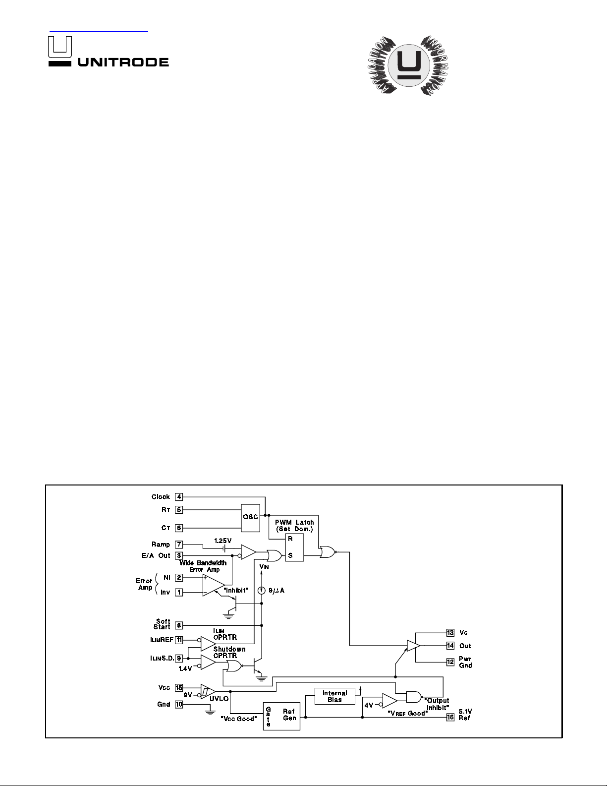
The UC1823 famil y of PWM control IC s is optimized for high frequency swi tched mode power suppl y applications. Par ticular care
was given to mini mizing propagation del ays through the comparators and logi c circuitry while maximizing bandwidth and slew rate
of the erro r amplifier. This controll er is designed for use in either
current-mode or voltage-mode systems with the capability for input
voltage feed-forward.
Protection circuitry includes a current limit comparator, a TTL compatible shu tdown port, and a soft start pin which will double as a
maximum duty cycl e clamp. The logic is full y latched to provi de jitter free operation and prohibit multiple pulses at the output. An under-voltage lockout section with 800mV of hysteresis assures low
start up current. During under-voltage lockout, the output is high impedance. The current limit reference (pin 11) is a DC input voltage to
the current limit com pa rat or. Con sult sp ecif icat ions for de tails.
These devices feature a totem pole output des igned to source and
sink high peak currents from capacitive loads, such as the gate of
a power MOSFET. The on state is defined as a high level.
ABSOLUTE MAXIMUM RATINGS
Supply Voltage (Pins 15, 13) . . . . . . . . . . . . . . . . . . . . . . . . 30V
Output Current, Source or Sink (Pin14)
DC. . . . . . . . . . . . . . . . . . . . . . . . . . . . . . . . . . . . . . . . . . 0.5A
Pulse (0.5µs). . . . . . . . . . . . . . . . . . . . . . . . . . . . . . . . . . 2.0A
Analog Inputs (Pins 1, 2, 7, 8, 9, 11) . . . . . . . . . . . -0.3V to +6V
Clock Output Current (Pin 4) . . . . . . . . . . . . . . . . . . . . . . . -5mA
Error Amplifier Output Current (Pin 3) . . . . . . . . . . . . . . . . 5mA
Soft Start Sink Current (Pin 8) . . . . . . . . . . . . . . . . . . . . . 20mA
Oscillator Charging Current (Pin 5) . . . . . . . . . . . . . . . . . . -5mA
Power Dissipation at TA = 60 °C . . . . . . . . . . . . . . . . . . . . . 1W
Storage Temperature Range . . . . . . . . . . . . . . -65°C to +150°C
Lead Temperature (Soldering, 10 seconds) . . . . . . . . . . 300°C
Note: All voltages are with respect to ground, Pin 10.
Currents are positive into the specified terminal.
Consult Packaging Section of Databook for thermal
limitations and considerations of packages.
BLOCK DIAGRAM
3/97
1
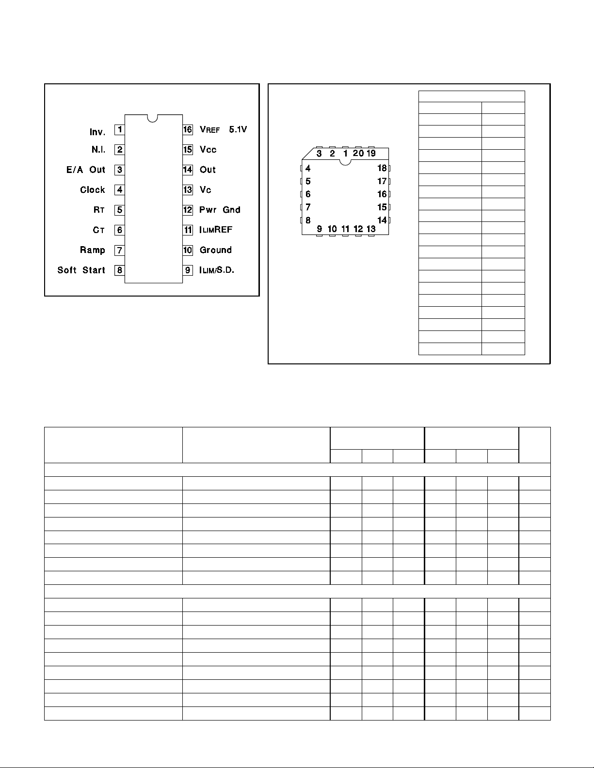
CONNECTION DIAGRAMS
UC1823
UC2823
UC3823
DIL-16, SOIC-16 (TOP VIEW)
J or N, DW Package
PLCC-20, LCC-20 (TOP VIEW)
Q, L Package
PACKAGE PIN FUNCTION
FUNCTION PIN
N/C 1
Inv. 2
N.I. 3
E/A Out 4
Clock 5
N/C 6
R
T
C
T
7
8
Ramp 9
Soft start 10
N/C 11
/S.D. 12
I
LIM
Ground 13
I
REF 14
LIM
PWR Gnd 15
N/C 16
V
C
17
OUT 18
V
CC
5.1V 20
V
REF
19
ELECTRICAL CHARACTERISTICS:
PARAMETER TEST CONDITIONS
Unless otherwise noted, these specifications apply for RT = 3.65k, CT =
CC
1nF, V
the UC2823, and -55°C < T
= 15V, 0°C < TA < +70°C for the UC3823, -25°C < TA < +85°C for
A
< +125°C for the UC1823, TA = T
UC1823
UC3823 UNITS
UC2823
J.
MIN TYP MAX MIN TYP MAX
Reference Section
Output Voltage T
Line Regulation 10 < V
Load Regulation 1 < I
Temperature Stability* T
= 25°C, lO = 1mA 5.05 5.10 5.15 5.00 5.10 5.20 V
J
< 30V 2 20 2 20 mV
CC
< 10mA 5 20 5 20 mV
O
< TA < T
MIN
MAX
0.2 0.4 0.2 0.4 mV/°C
Total Output Variation* Line, Load, Temp. 5.00 5.20 4.95 5.25
Output Noise Voltage* 10Hz < f < 10kHz 50 50 µV
Long Term Stability* T
Short Circuit Current V
= 125°C, 1000 hrs. 5 25 5 25 mV
J
=0V -15 -50 -100 -15 -50 -100 mA
REF
Oscillator Section
Initial Accuracy * T
Voltage Stability* 10 < V
Temperature Stability* T
=25°C 360 400 440 360 400 440 kHz
J
< 30V 0.2 2 0.2 2 %
CC
MIN
<TA < T
MAX
55%
Total Variation* Line, Temp. 340 460 340 460 kHz
Clock Out High 3.9 4.5 3.9 4.5 V
Clock Out Low 2.3 2.9 2.3 2.9 V
Ramp Peak* 2.6 2.8 3.0 2.6 2.8 3.0 V
Ramp Valley* 0.7 1.0 1.25 0.7 1.0 1.25 V
Ramp Valley to Peak* 1.6 1.8 2.0 1.6 1.8 2.0 V
* These parameters are guara nt ee d by des ig n bu t no t 10 0% te sted in production.
2
ELECTRICAL CHARACTERISTICS:
Unless otherwise noted, these specifications apply for R
T
= 3.65k, CT = 1nF, V
= 15V, 0°C < TA < +70°C for the UC3823, -25°C < TA < +85°C for the
UC2823, and -55°C < T
A
< +125°C for the UC1823, TA = T
J.
UC1823
UC2823
UC3823
CC
PARAMETER TEST CONDIT IONS
UC1823
UC2823
UC3823 UNITS
MIN TYP MAX MIN TYP MAX
Error Amplifier Section
Input Offset Voltage 10 15 mV
Input Bias Current 0.6 3 0.6 3 µA
Input Offset Current 0.1 1 0.1 1 µA
Open Loop Gain 1 < V
CMRR 1.5 < V
PSRR 10 < V
Output Sink Current V
Output Source Current V
Output High Voltage I
Output Low Voltag e I
< 4V 60 95 60 95 dB
O
< 5.5V 75 95 75 95 dB
CM
< 30V 85 110 85 110 dB
CC
=1V 1 2.5 1 2.5 mA
PIN 3
= 4V -0.5 -1.3 -0.5 -1.3 mA
PIN 3
= −0.5mA 4.0 4.7 5.0 4.0 4.7 5.0 V
PIN 3
= 1mA 0 0.5 1.0 0 0.5 1.0 V
PIN 3
Unity Gain Bandwidth* 3 5.5 3 5.5 MHz
Slew Rate* 6 12 6 12 V/µS
PWM Comparator Section
Pin 7 Bias Current V
= 0V -1 -5 -1 -5 µA
PIN 7
Duty Cycle Range 0 80 0 85 %
Pin 3 Zero D.C. Threshold V
= 0V 1.1 1.25 1.1 1.25 V
PIN 7
Delay to Output* 50 80 50 80 ns
Soft-Start Section
Charge Current V
Discharge Current V
= 0.5V 3 9 20 3 9 20 µA
PIN 8
= 1V 1 1 mA
PIN 8
Current Limit/Shutdown Section
Pin 9 Bias Current 0 < V
Current Limit Offset V
PIN 11
Current Limit Common Mode
Range (V
PIN 11
)
< 4V ±10 ±10 µA
PIN 9
= 1.1V 15 15 mV
1.0 1.25 1.0 1.25 V
Shutdown Threshold 1.25 1.40 1.55 1.25 1.40 1.55 V
Delay to Output* 50 80 50 80 ns
Output Section
Output Low Level I
Output High Level I
Collector Leakage V
= 20mA 0.25 0.40 0.25 0.40 V
OUT
= 200mA 1.2 2.2 1.2 2.2 V
I
OUT
= −20mA 13.0 13.5 13.0 13.5 V
OUT
I
= −200mA 12.0 13.0 12.0 13.0 V
OUT
= 30V 100 500 100 500 µA
C
Rise/Fall Time* CL = 1nF 3060 3060ns
Under-Voltage Lockout Section
Start Threshold 8 .8 9.2 9.6 8.8 9.2 9.6 V
UVLO Hysteresis 0.4 0.8 1.2 0.4 0.8 1.2 V
Supply Current
Start Up Current V
I
CC
= 8V 1.1 2.5 1.1 2.5 mA
CC
V
PIN 1
, V
PIN 7, VPIN 9
=0V, V
= 1V 22 33 22 33 mA
PIN 2
* These parameters are guara nt ee d by des ig n bu t no t 10 0% te sted in production.
3
 Loading...