

UC1727
UC2727
UC3727
查询UC1727供应商
Isolated High Side IGBT Driver
FEATURES DESCRIPTION
• Receives Power and Signal from Single
Isolation Transformer
• Generates Split Rail for 4A Peak Bipolar
Gate Drive
• 16V High Level Gate Drive
• Low Level Gate Drive more Negative
than -5V
• Undervoltage Lockout
• Desaturation Detection and Fault
Processing
• Separate Output Enable Input
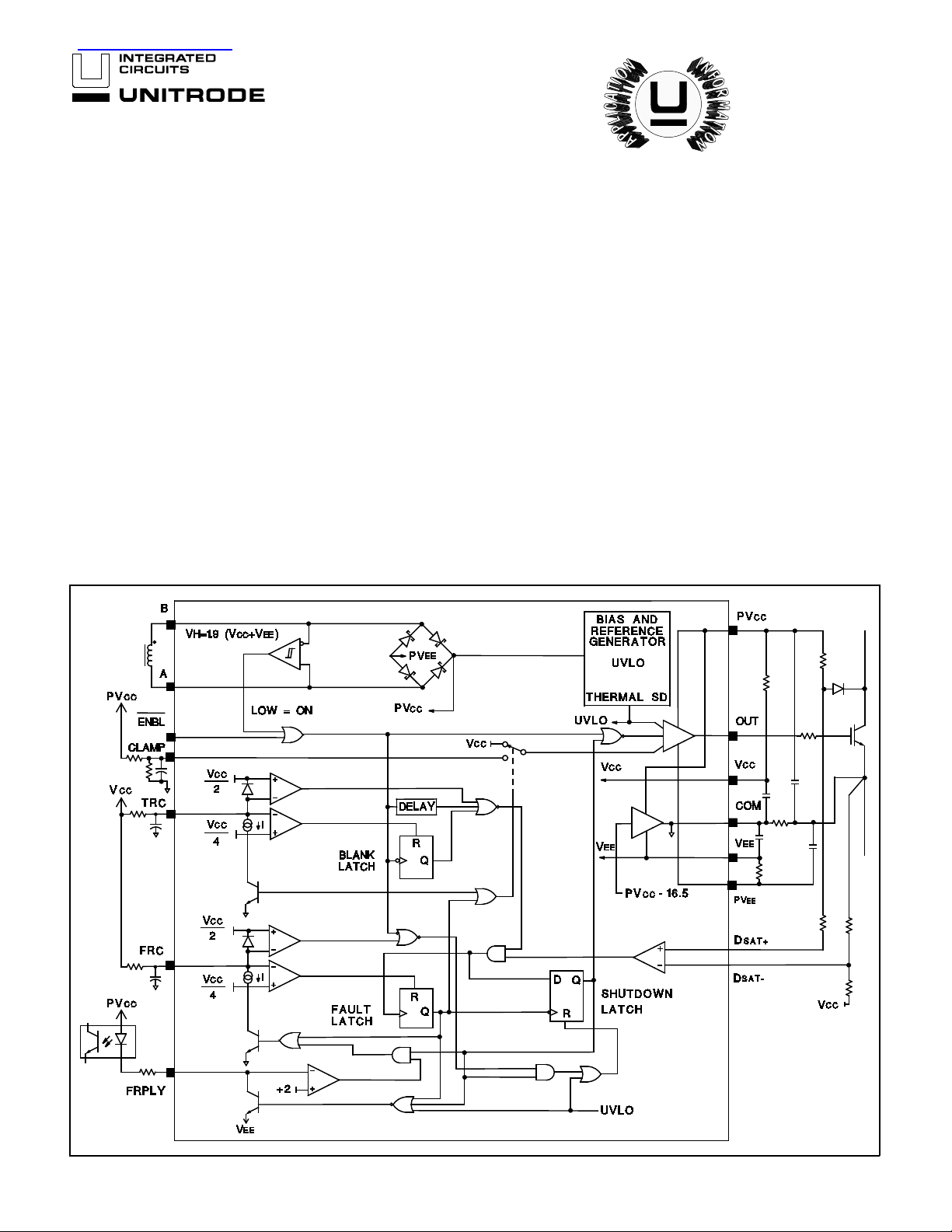
The UC1727 and its companion chip, the UC1726, provide all the
necessary features to drive an isolated IGBT transistor from a TTL input signal. A unique modulation scheme is used to transmit both
power and signal across an isolation boundary with a minimum of external components.
Protection features include under voltage lockout and desaturation
detection. High level gate drive signals are typically 16V. Intermediate
high drive level s can be programmed for various periods of time to
limit surge current at turn on and in the event of desaturation due to a
short circuit.
The chip generates a bipolar supply so that the gate can be driven to
a negative vol tage insuring the I GBT remains off in the presence of
high common mode slew rates.
• Programmable Stepped Gate Drive for
Soft Turn On
• Programmable Stepped Gate Drive for
Soft Fault
BLOCK DIAGRA M
Uses include isolated off-line full bridge and half bridge drives for motors, switches, and any other load requiring full electrical isolation.
12/94
UDG-94005-2
ABSOLUTE MAXI MUM RATING S
Supply voltage (V CC - VEE). . . . . . . . . . . . . . . . . . . . . . . . . . . . . . . . . . . . . 40V
Power Inpu ts (|A - B|). . . . . . . . . . . . . . . . . . . . . . . . . . . . . . . . . . . . . . . . . 45V
Analog Input Voltage (
Analog Input Voltage ( D
Analog Input Curren t (D
ENBL, CLAMP). . . . . . . . . . . . . . . . . . -0.3 To Vcc+0.3
SAT+, DSAT-) . . . . . . . . . . . . . . . . VEE-0.3 to VCC+0.3
SAT+, DSAT-) . . . . . . . . . . . . . . . . . . . . . . -10 to 10mA
Output Current, (OUT)
DC . . . . . . . . . . . . . . . . . . . . . . . . . . . . . . . . . . . . . . . . . . . . . . . . . . . . 0.8A
Pulse (0.5µs) . . . . . . . . . . . . . . . . . . . . . . . . . . . . . . . . . . . . . . . . . . . . . . 4A
FRPLY Output Curr ent. . . . . . . . . . . . . . . . . . . . . . . . . . . . . . . . . . . . . . 30mA
Note: All voltages ar e w ith respe ct to CO M. Curre nt s are pos itive int o the
specified terminal.
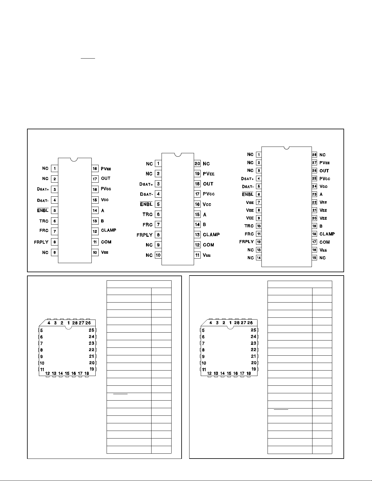
CONNECTION DIAGRAMS
DIL-18 (Top View)
J Package
DIL-20 (Top View)
N Package
UC1727
UC2727
UC3727
SOIC-28 (Top View)
DWP Package
PLCC-28 (Top View)
QP Package
PACKAGE PIN FUNCTION
FUNCTION PIN
N/C 1
V
EE 2
N/C 3-4
COM 5
CLAMP 6
B7
A8
V
CC 9
PV
CC 10
OUT 11
PV
EE 12-18
D
SAT+ 19
D
SAT- 20
ENBL 21
NC 22
TRC 23
FRC 24
FRPLY 25
N/C 26
N/C 27
N/C 28
LCC-28 (Top View )
LP Package
PACKAGE PIN FUNCTION
FUNCTION PIN
N/C 1
V
EE 2
N/C 3-4
COM 5
CLAMP 6
B7
A8
V
CC 9
PV
CC 10
OUT 11
N/C 12-13
PV
EE 14
N/C 15-18
D
SAT+ 19
D
SAT- 20
ENBL 21
NC 22
TRC 23
FRC 24
FRPLY 25
N/C 26-28
2
Unless otherw ise stat ed, these sp ecif icat io ns apply for TA = −55 °C to 125°C for the
UC1727, TA = −40°C to 85°C for the UC2727, TA = 0°C to 70° C for the UC3727,
R(TRC) = 54.9k, C(TRC) = 180pF , R(FRC) = 309K, C(FRC) = 200pF, VCC - VEE =
25V, CLAMP = 9V, TA = TJ, and all voltage s are mea sur ed with respect to COM.
See Application Note U-143A "Ne w Chi p Pair Pro vides Iso lated Driv e for High Volta ge IGBTs"
PIN DESCRIP TI ONS
A, B: Signal and power input pins. Connect these pins to
the secondary of the transformer driven by UC1726.
CLAMP: Analog programming pin for intermediate drive
level to be used at turn on or in response to a desaturation event. Requires a bypass capacitor to COM.
FRPLY: Fault Reply pin. Open coll ector output. Normally
connected to V
EE. When desaturation is detected, the pin
opens.
OUT: Gate drive output. Connect to gate of IGBT with a
series damping resistor greater than 3 ohms.
UC1727
UC2727
UC3727
COM: Self generated common for bipolar supply. This
pin will be 16.5V below PV
D
SA T + , DSAT-: Inputs to the desaturation comparator. De-
saturation is detected when D
CC.
SA T+ is greater than D SAT-.
ENBL: Negative true enable input. Tie to VCC to disable
the chip. Connect to COM to enable the chip. If the
ENBL
pin is used as the primary input to the chip, connect B to
V
CC and A to V EE.
FRC: Fault Resistor and Capacitor. Programs the duration that OUT will be held at CLAMP potential during a desaturation event before it is driven fully low. Also sets the
period of time tha t OUT will be held low before allowing it
to be driven high again.
TRC: Timing Resistor and Capacitor. Programs the duration that OUT will be held at CLAMP potential and the period of time the desaturation comparator will be ignored
during the rising edge.
V
CC: Positive supply voltag e. Bypass to COM with a low
ESL/ESR 1µF capacitor.
EE: Negative supply voltage. Bypass to COM with a low
V
ESL/ESR 1µF capacitor.
EE: Output driver negative supply. Connect to VEE
PV
with a 3.3 ohm resistor and bypass to COM with a low
ESL/ESR 1µF capacitor.
CC: Output driver positive supply. Connect to VCC with
PV
a 3.3 ohm resistor and bypass to COM with a low
ESL/ESR 1µF capacitor.
ELECTRICAL CHARACTERISTICS:
PARAMETER TEST CONDITIONS MIN TYP MAX UNITS
Power Input Receivers
Forward Diode Dro p I
V
CC Regulator
V
CC 25 ≤ (VCC - VEE) ≤ 36V,I(COM) ≤ 15mA 15.5 16.5 17.5 V
Hysteresi s Compar at or
Input Open Circuit Voltag e (Measured with respe ct to V
Input Impedance 100 kΩ
Hysteresis 44 47 50 V
Enable Input
High Level Input Voltage 12 V
Low Level Input Volta ge 5V
Input Bias Cur rent
Output Driver
Saturation to V
Saturation to V
Saturation to V
Saturation to V
CC I(OU T ) = -20 mA 1.7 2.3 V
CC I(OU T ) = -50 0m A 2 2.5 V
EE I(OU T) = 20mA 2 3 V
EE I(OU T) = 500mA 2.4 3.6 V
F = 50mA 0.5 0.65 V
I
F = 500mA 1.2 2 V
EE)12V
ENBL = COM −460 −900 µA
3
 Loading...