

查询5962-0051401QEA供应商
Dual Non-Inverting Power Driver
FEATURES DESCRIPTION
3.0A Peak Current Totem Pole
•
Output
5 to 35V Operation
•
25ns Rise and Fall Times
•
25ns Propagation Delays
•
Thermal Shutdown and Under-
•
Voltage Protection
High-Speed, Power MOSFET
•
Compatible
Efficient High Frequency Operation
•
Low Cross-Conduction Current
•
Spike
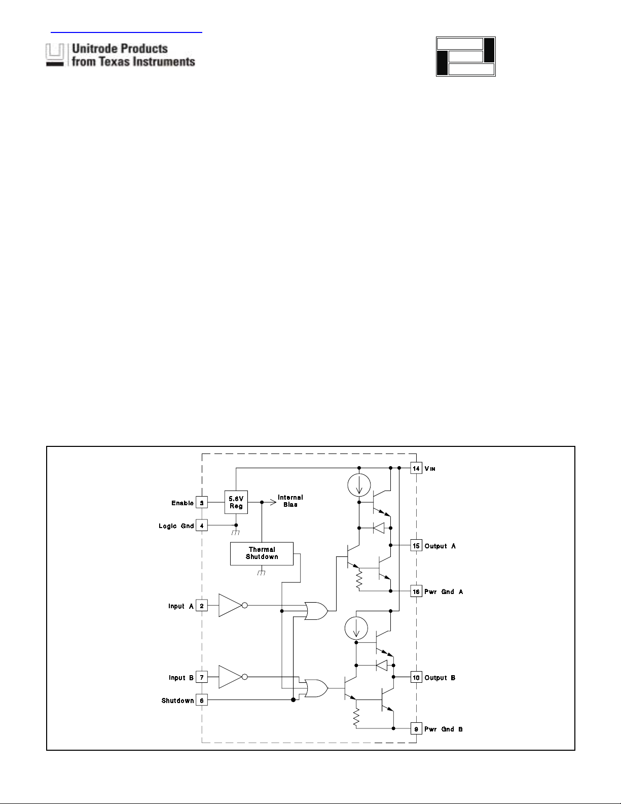
The UC1708 family of power drivers is made with a high-speed,
high-voltage, Schottky process to interface control functions and high-power
switching devices – particularly power MOSFETs. Operating over a 5 to 35
volt supply range, these devices contain two independent channels. The A
and B inputs are compatible with TTL and CMOS logic families, but can
withstand input voltages as high as V
to 3A as long as power dissipation limits are not exceeded.
Although each output can be activated independently with its own inputs,
they can be forced low in common through the action of either a digital high
signal at the Shutdown terminal or by forcing the Enable terminal low. The
Shutdown terminal will only force the outputs low, it will not effect the behav
ior of the rest of the device.The Enable terminal effectively places the device
in under-voltage lockout, reducing power consumption by as much as 90%.
During under-voltage and disable (Enable terminal forced low) conditions,
the outputs are held in a self-biasing, low-voltage, state.
application
INFO
available
IN. Each output can source or sink up
UC1708
UC2708
UC3708
-
• Enable and Shutdown Functions
• Wide Input Voltage Range
• ESD Protection to 2kV
BLOCK DIAGRAM
The UC3708 and UC2708 are available in plastic 8-pin MINI DIP and 16-pin
“bat-wing” DIP packages for commercial operation over a 0
perature range and industrial temperature range of -25
respectively. For operation over a -55
UC1708 is available in hermetically sealed 8-pin MINI CDIP, 16 pin CDIP
and 20 pin CLCC packages.Surface mount devices are also available.
o
C to +125oC temperature range, the
o
Cto+70oC tem-
o
Cto+85oC
Note: Shutdown feature is not available in J or N packages only.
SLUS171A - MARCH 1997 - REVISED AUGUST 2001
UDG-92024-1
UC1708
UC2708
UC3708
ABSOLUTE MAXIMUM RATINGS (Note 1)
Supply Voltage VIN . . . . . . . . . . . . . . . . . . . . . . . . . . . . . . . . . . . . . . . . . . . . . . . . . . . . . . . . . . . . . . . . . . . . . . . . . . . . . . . . . . . . 35V
Output Current (Each Output, Source or Sink)
Steady-State . . . . . . . . . . . . . . . . . . . . . . . . . . . . . . . . . . . . . . . . . . . . . . . . . . . . . . . . . . . . . . . . . . . . . . . . . . . . . . . . . . . . . . 0.5A
Peak Transient . . . . . . . . . . . . . . . . . . . . . . . . . . . . . . . . . . . . . . . . . . . . . . . . . . . . . . . . . . . . . . . . . . . . . . . . . . . . . . . . . . . . . . 3A
Ouput Voltage . . . . . . . . . . . . . . . . . . . . . . . . . . . . . . . . . . . . . . . . . . . . . . . . . . . . . . . . . . . . . . . . . . . . . . . . . . .
Enable and Shutdown Inputs . . . . . . . . . . . . . . . . . . . . . . . . . . . . . . . . . . . . . . . . . . . . . . . . . . . . . . . . . . . . . . . . . . . . . .
A and B Inputs . . . . . . . . . . . . . . . . . . . . . . . . . . . . . . . . . . . . . . . . . . . . . . . . . . . . . . . . . . . . . . . . . . . . . . . . . . .
Operating Junction Temperature (Note 2) . . . . . . . . . . . . . . . . . . . . . . . . . . . . . . . . . . . . . . . . . . . . . . . . . . . . . . . . . . . . . . . . 150°C
Storage Temperature Range. . . . . . . . . . . . . . . . . . . . . . . . . . . . . . . . . . . . . . . . . . . . . . . . . . . . . . . . . . . . . . . . . . . . . -65° to 150°C
Lead Temperature (Soldering, 10 Seconds). . . . . . . . . . . . . . . . . . . . . . . . . . . . . . . . . . . . . . . . . . . . . . . . . . . . . . . . . . . . . . . 300°C
-0.3 to (VIN + 0.3)V
-0.3 to 6.2V
-0.3 to (VIN + 0.3)V
NOTE 1: All voltages are with respect to Logic Gnd pin.All currents are positive into, negative out of, device terminals.
NOTE 2:Consult Unitrode Integrated Circuits databook for information regarding thermal specifications and limitations of packages.
CONNECTION DIAGRAMS
DIL-8 (Top View)
J Or N Package
DIL-16 (Top View)
JE or NE Package
SOIC-16 (Top View)
DW Package
CLCC-20 (Top View)
L Package
INPUT A
N/C
N/C
PWR GND A
OUTPUT A
Note: In JE package Pin 4 is logic ground. Pins 5, 12,
and 13 are N/C.
N/C
N/C
20 19
PWR GND B
18
17
16
15
14
OUTPUT B
VIN
N/C
N/C
N/C
VIN
ENABLE
LOGIC GND
N/C 6
N/C
SHUTDOWN
321
4
5
7
8
910111213
INPUT B
2
UC1708
UC2708
UC3708
ELECTRICAL CHARACTERISTICS: Unless otherwise stated, V
for: –55
o
C<TA<125oC for the UC1708, –25oC<TA<+85oC for the UC2708, and 0oC<TA<70oC for the UC3708.TA =TJ.
=10V to 35V, and these specifications apply
IN
PARAMETER TEST CONDITIONS MIN TYP MAX UNITS
IN Supply Current OutputsLow 18 26 mA
V
Outputs High 14 18 mA
Enable = 0V 1 4 mA
A, B and Shutdown Inputs Low
0.8 V
Level
A, B and Shutdown Inputs High
2.0 V
Level
A, B Input Current Low V
A, B Input Current High V
A, B Input Leakage Current High V
Shutdown Input Current Low V
Shutdown Input Current High V
Enable Input Current Low V
Enable Input Current High V
A,B = 0.4V -1 -0.6 mA
A,B = 2.4V -200 50 µA
A,B = 35.3V 200 µA
SHUTDOWN = 0.4V 20 100 µA
SHUTDOWN = 2.4V 170 500 µA
SHUTDOWN = 6.2V 0.6 1.5 mA
V
ENABLE = 0V -600 -460 200 µA
ENABLE = 6.2V 200 µA
Enable Threshold Rising 2.8 3.6 V
Enable Threshold Falling 1.0 2.4 3.4 V
Output High Sat., V
Output Low Sat., V
IN -VOUT IOUT = -50mA 2.0 V
OUT = -500mA 2.5 V
I
OUT IOUT = 50mA 0.5 V
OUT = 500mA 2.5 V
I
Thermal Shutdown 155 °C
SWITCHING CHARACTERISTICS (Figure 1), (VIN = 20V, delays measured to 10% output change.)
PARAMETER TEST CONDITIONS MIN TYP MAX UNITS
From A,B Input to Output:
Rise Time Delay (TPLH) CL = 0pF 25 40 ns
CL = 1000pF (Note 3) 25 40 ns
CL = 2200pF 30 45 ns
10% to 90% Rise (TTLH) CL = 0pF 55 75 ns
CL = 1000pF (Note 3) 25 50 ns
CL = 2200pF 40 55 ns
Fall Time Delay (TPHL) CL = 0pF 25 40 ns
CL = 1000pF (Note 3) 25 45 ns
CL = 2200pF 35 50 ns
90% to 10% Fall (TTHL) CL = 0pF 15 20 ns
CL = 1000pF (Note 3) 25 45 ns
CL = 2200pF 40 55 ns
NOTE 3: These parameters, specified at 1000pF, although ensured over recommended operating conditions, are not tested in
production.
3
UC1708
UC2708
UC3708
SWITCHING CHARACTERISTICS (Figure 1), (VIN = 20V, delays measured to 10% output change.)
From Shutdown Input to Output
Rise Time Delay (TPLH) CL = 0pF 25 75 ns
CL = 1000pF (Note 3) 30 75 ns
CL = 2200pF 35 75 ns
10% to 90% Rise (TTLH) CL = 0pf 50 75 ns
CL = 1000pF (Note 3) 25 50 ns
CL = 2200pF 40 55 ns
Fall Time Delay (TPHL) CL = 0pF 25 45 ns
CL = 1000pF (Note 3) 30 50 ns
CL = 2200pF 35 55 ns
90% to 10% Fall (TTHL) CL = 0pF 25 20 ns
CL = 1000pF (Note 3) 25 45 ns
CL = 2200pF 40 55 ns
Total Supply Current F = 200kHz, 50% duty cycle, both channels; CL = 0pF 23 25 mA
F = 200kHz, 50% duty cycle, both channels; CL = 2200pF 38 45 mA
NOTE 3: These parameters, specified at 1000pF, although ensured over recommended operating conditions, are not tested in
production.
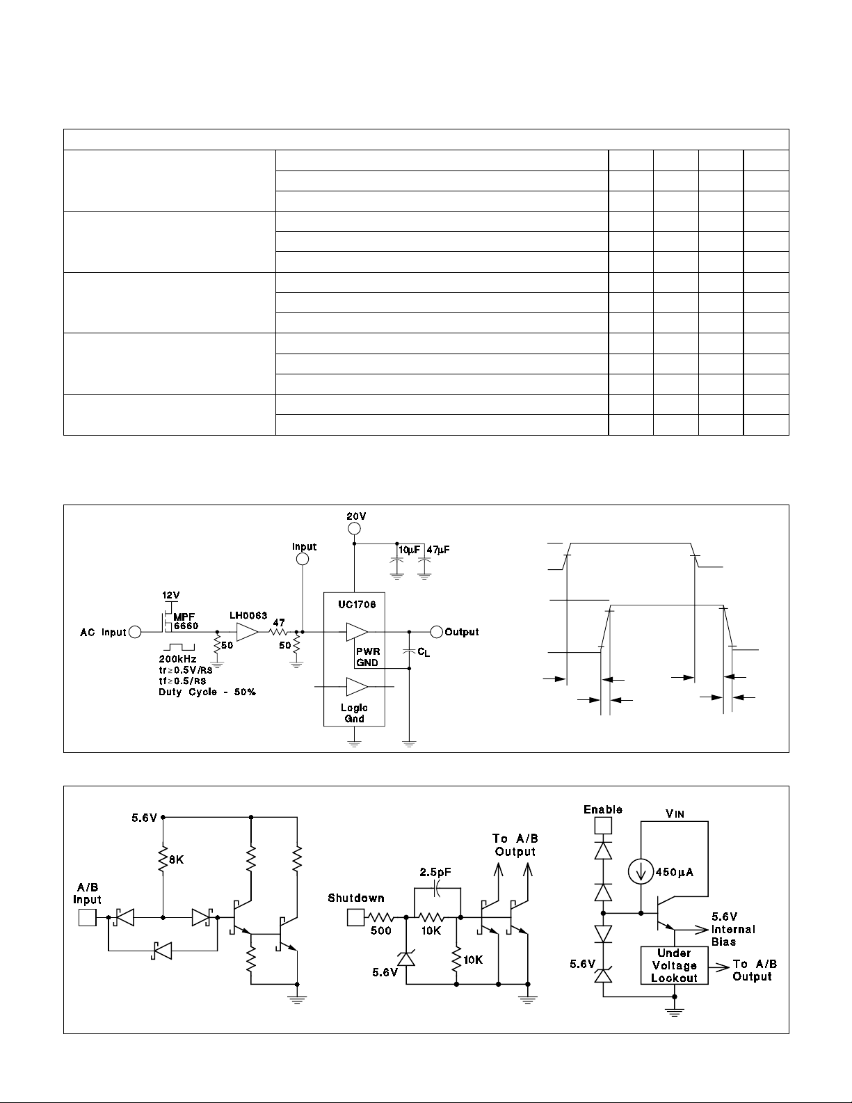
Figure 1: AC Test Circuit and Switching Time Waveforms
Figure 2: Equivalent Input Circuits
4.3V
INPUT
OUTPUT
TP
0V
20V
0V
LH
50%
90%
10%
TP
HL
TT
LH
50%
90%
10%
TT
HL
UDG-92026
Note: Shutdown feature available only in JE, NE or DW Packages.
UDG-92025
4
PACKAGE OPTION ADDENDUM
www.ti.com
PACKAGING INFORMATION
Orderable Device Status
5962-0051401Q2A ACTIVE LCCC FK 20 1 TBD POST-PLATE Level-NC-NC-NC
5962-0051401QEA ACTIVE CDIP J 16 1 TBD A42 SNPB Level-NC-NC-NC
5962-0051401QPA ACTIVE CDIP JG 8 1 TBD A42 SNPB Level-NC-NC-NC
5962-0051401V2A ACTIVE LCCC FK 20 1 TBD Call TI Level-NC-NC-NC
5962-0051401VEA ACTIVE CDIP J 16 1 TBD Call TI Level-NC-NC-NC
5962-0051401VPA ACTIVE CDIP JG 8 1 TBD A42 Level-NC-NC-NC
UC1708J ACTIVE CDIP JG 8 1 TBD A42 SNPB Level-NC-NC-NC
UC1708J883B ACTIVE CDIP JG 8 1 TBD A42 SNPB Level-NC-NC-NC
UC1708JE ACTIVE CDIP J 16 1 TBD A42 SNPB Level-NC-NC-NC
UC1708JE883B ACTIVE CDIP J 16 1 TBD A42 SNPB Level-NC-NC-NC
UC1708L883B ACTIVE LCCC FK 20 1 TBD POST-PLATE Level-NC-NC-NC
UC2708D OBSOLETE UTR TBD Call TI Call TI
UC2708DW ACTIVE SOIC DW 16 40 Green (RoHS &
UC2708DWG4 ACTIVE SOIC DW 16 40 Green (RoHS &
UC2708DWTR ACTIVE SOIC DW 16 2000 Green(RoHS &
UC2708DWTRG4 ACTIVE SOIC DW 16 2000 Green (RoHS &
UC2708J OBSOLETE UTR TBD Call TI Call TI
UC2708JE OBSOLETE UTR TBD Call TI Call TI
UC2708N ACTIVE PDIP P 8 50 Green (RoHS &
UC2708NE ACTIVE PDIP N 16 25 Green (RoHS &
UC2708NG4 ACTIVE PDIP P 8 50 Green (RoHS &
UC2708Q OBSOLETE UTR TBD Call TI Call TI
UC3708DW ACTIVE SOIC DW 16 40 Green (RoHS &
UC3708DWG4 ACTIVE SOIC DW 16 40 Green (RoHS &
UC3708DWTR ACTIVE SOIC DW 16 2000 Green(RoHS &
UC3708DWTRG4 ACTIVE SOIC DW 16 2000 Green (RoHS &
UC3708J ACTIVE CDIP JG 8 1 TBD A42 SNPB Level-NC-NC-NC
UC3708JE ACTIVE CDIP J 16 1 TBD A42 SNPB Level-NC-NC-NC
UC3708N ACTIVE PDIP P 8 50 Green (RoHS &
UC3708NE ACTIVE PDIP N 16 25 Green (RoHS &
UC3708NEG4 ACTIVE PDIP N 16 25 Green (RoHS &
UC3708NG4 ACTIVE PDIP P 8 50 Green (RoHS & CU NIPDAU Level-NC-NC-NC
(1)
Package
Type
Package
Drawing
Pins Package
Qty
Eco Plan
no Sb/Br)
no Sb/Br)
no Sb/Br)
no Sb/Br)
no Sb/Br)
no Sb/Br)
no Sb/Br)
no Sb/Br)
no Sb/Br)
no Sb/Br)
no Sb/Br)
no Sb/Br)
no Sb/Br)
no Sb/Br)
(2)
Lead/Ball Finish MSL Peak Temp
CU NIPDAU Level-2-260C-1YEAR
CU NIPDAU Level-2-260C-1YEAR
CU NIPDAU Level-2-260C-1YEAR
CU NIPDAU Level-2-260C-1YEAR
CU NIPDAU Level-NC-NC-NC
Call TI Level-NC-NC-NC
CU NIPDAU Level-NC-NC-NC
CU NIPDAU Level-2-260C-1YEAR
CU NIPDAU Level-2-260C-1YEAR
CU NIPDAU Level-2-260C-1YEAR
CU NIPDAU Level-2-260C-1YEAR
CU NIPDAU Level-NC-NC-NC
Call TI Level-NC-NC-NC
Call TI Level-NC-NC-NC
4-Nov-2005
(3)
Addendum-Page 1
 Loading...