

查询UC1635供应商
Phase Locked Frequency Co ntroller
FEATURES DESCRIPTION
•
Precision Phase Locked Frequency
Control System
•
Crystal Oscillator
•
Programmable Reference Frequency
Dividers
•
Phase Detector with Absolute Frequency
Steering
•
Separate Divider Outputs and Phase
Detector Input Pins
•
Double Edge Option on the Frequency
Feedback Sensing Amplifier
•
Two High Current Op Amps
•
5V Reference Output
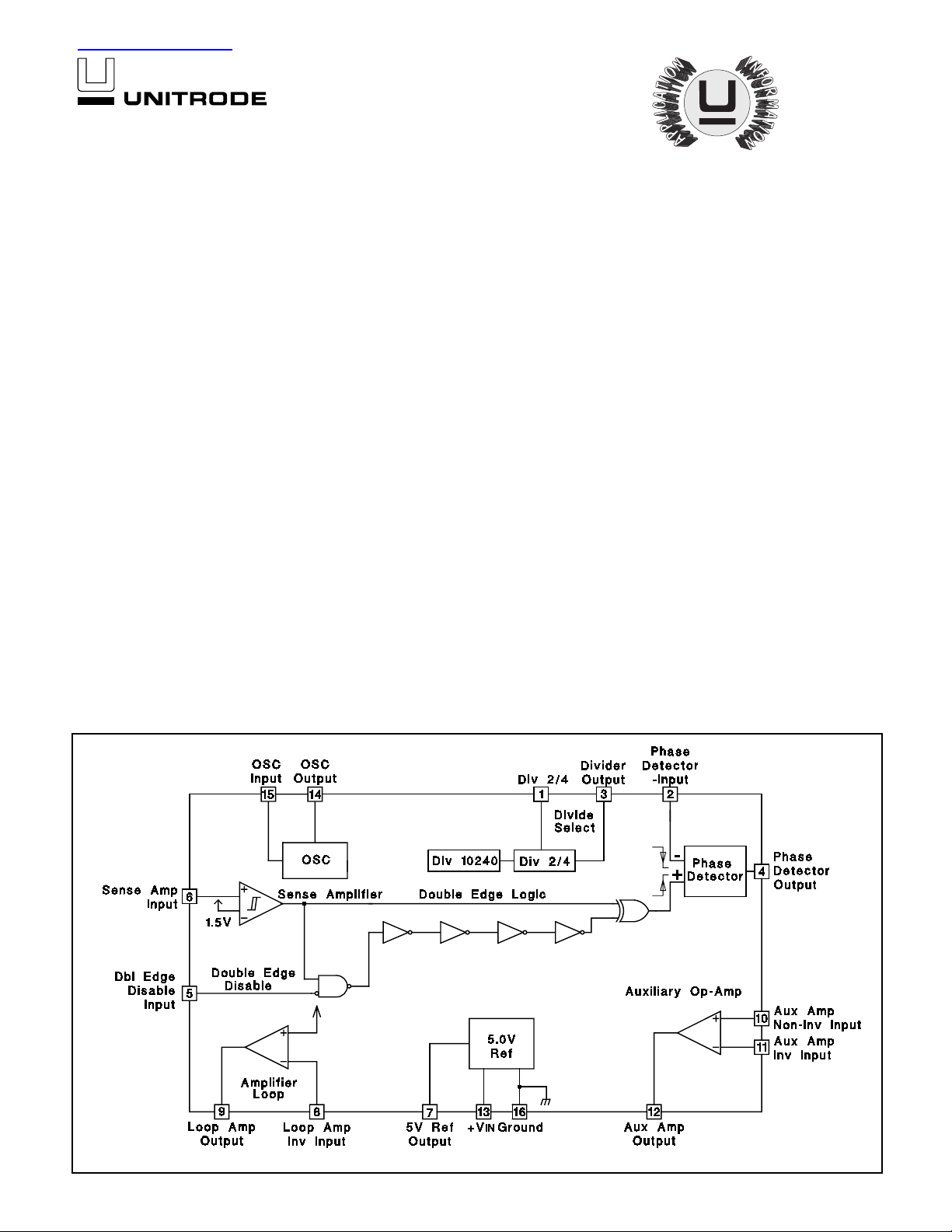
The UC1635 fa mily of i ntegra ted circui ts was desi gned for use in precision speed c ontrol of DC motors. An extension to the UC1633 line of
phase locked controllers, these devices provide access to both of the
digital phase detector ’s inputs, and include a reference frequency divider output pin. With this added flexibility, this family of controllers can
be used to obtain phase synchronization of multiple motors.
A reference frequency can be generated using the device’s crystal oscillator and pro grammabl e divide rs. The osc illator operates using a broad
range of cr ystals, or, can functi on as a buffer stage to an external frequency source.
The phase de tector responds proportional ly to the phase error between
the detector’s minus input pin and the sense amplifier output. This
phase detector includes absolute frequency steering to provide maximum drive sign als when any frequency error exists. This feature allows
optimum start-up and lock times to be realized.
UC1635
UC2635
UC3635
BLOCK DIAGRAM
Two op-amps are included that can be confi gure d to provide necessary
loop filtering. The outputs of these op-amps will source or sink in excess
of 16mA, s o they c an pr ovide a low i mpedan ce cont rol signal to driving
circuits.
Additional features include a double edge option on the sens e amplifier
that can be used to doubl e the loop reference frequency for increased
loop bandwi dths. A 5V reference output can be used to accurately set
DC operating levels.
7/97
UDG-92019
UC1635
UC2635
UC3635
ABSOLUTE MAXIMUM RATINGS
Input Supply Voltage (+VIN) . . . . . . . . . . . . . . . . . . . . +20V
Reference Output Current . . . . . . . . . . . . . . . . . . . . . -30mA
Op-Amp Output Currents . . . . . . . . . . . . . . . . . . . . ±30mA
Op-Amp Input Voltages . . . . . . . . . . . . . . . . . . -0.3 to +20V
Phase Detector Input Voltage . . . . . . . . . . . . . -0.3V to +5V
Phase Detector Output Current . . . . . . . . . . . . . . . . ±10mA
Lock Indicator Output Current . . . . . . . . . . . . . . . . . +15mA
Lock Indicator Output Voltage . . . . . . . . . . . . . . . . . . . +20V
Divide Select Input Voltages . . . . . . . . . . . . -0.3V to +10V
Double Edge Disable Input Voltage . . . . . . . -0.3V to +10V
Oscillator Input Voltage . . . . . . . . . . . . . . . . . . -0.3V to +5V
Sense Amplifier Input Voltage . . . . . . . . . . . . -0.3V to +20V
Power Dissipation at TA = 25°C, (Note 2) . . . . . . . 1000mW
Power Dissipation at TC = 25°C, (Note 2) . . . . . . . 2000mW
Operating Junction Temperature . . . . . . . . . -55° to 150°C
Storage Temperature . . . . . . . . . . . . . . . . . -65° to +150°C
Lead Temperature (Soldering, 10 Seconds) . . . . . . . 300°C
Note 1: Vo lt ag es are ref ere nc ed to gro un d, (Pin 16). Currents
are positive into, negative out of, the specified terminals.
Note 2: Consult Uni tro de Int eg rated Circuits databook for in formation regarding therm al specifications and limitations of
packages.
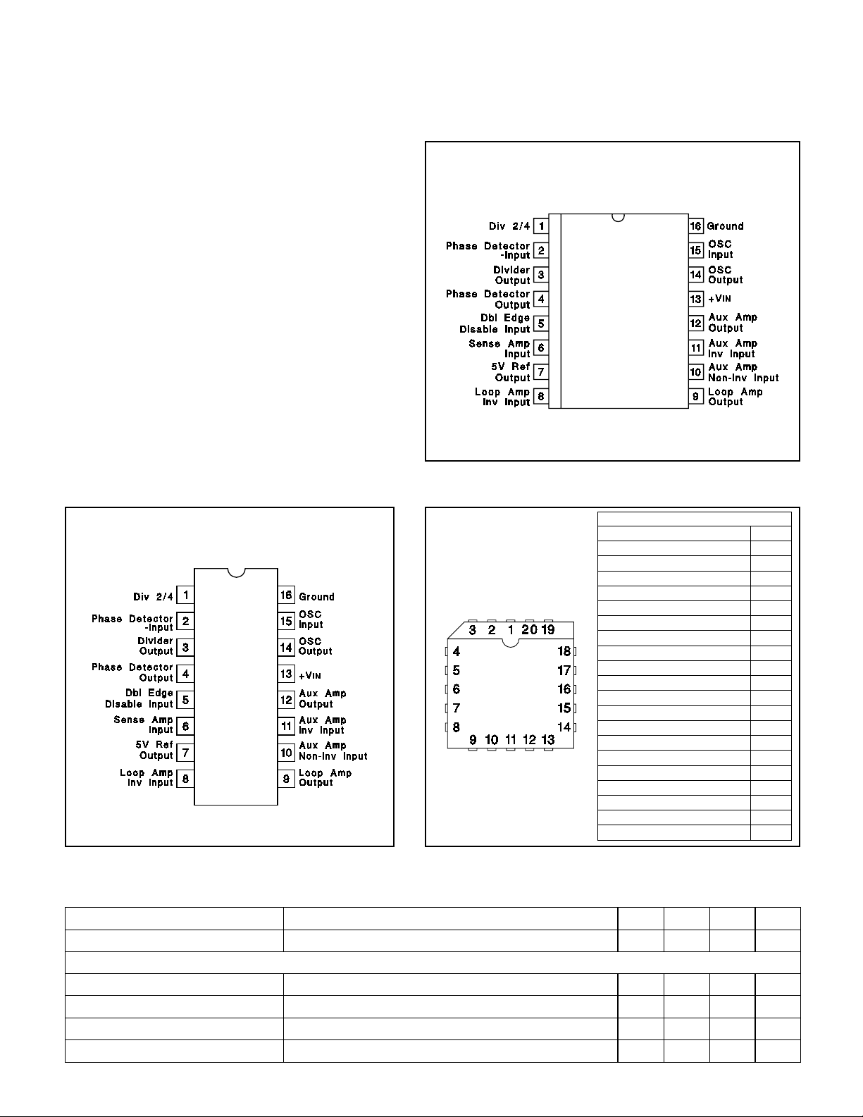
DIL–16 (Top View)
J & N Packages
CONNECTION DIAGRAMS
SOIC–16 (Top View)
DW Package
PLCC-20 & LCC-20
(Top View)
Q & L Packages
N/C 1
Div 2/4 2
Phase Detector Input 3
Divider Output 4
Phase Detector Output 5
N/C 6
Dbl Edge Disable Input 7
Sense Amp Input 8
5V Ref Output 9
Loop Amp Inv Input 10
N/C 11
Loop Amp Output 12
Aux Amp Non-Inv Input 13
Aux Amp Inv Input 14
Aux Amp Output 15
N/C 16
+V
OSC Output 18
OSC Input 19
Ground 20
PACKAGE PIN FUNCTION
FUNCTION
IN
PIN
17
ELECTRICAL
CHARACTERISTICS:
PARAMETER TEST CONDITIONS MIN TYP MAX UNITS
Supply Current +VIN = 15V 20 28 mA
Reference
Output Voltage (V
Load Regulation I
Line Regulation +V
Short Circuit Current V
REF
Unless otherwise stated, specifications hold for T
the UC2635 and -55°C to +125°C for the UC1635, +V
) 4.75 5.0 5.25 V
= 0 to 7mA 5.0 20 mV
OUT
= 8 to 15V 2.0 20 mV
IN
= 0V 15 35 mA
OUT
= 0°C to +70°C for the UC3635, -25°C to +85°C for
A
= 12V. TA = T
IN
J.
2
 Loading...