

DESCRIPTIO N
This four-diod e array is designed for general purpose use as individual
diodes or as a high-speed, high-current bridge. It is particularly useful on
the outputs of high-speed power MOSFET drivers where Schottky diodes
are neede d to clamp any ne gative excursi ons caused by ringing on the
driven line.
These diodes are also ideally suited for use as voltage clamps when driv ing inductive loads such as relays and solenoids, and to provide a path
for current free-wheeling in motor drive applications.
The use of Schottky diode technology fea tures high efficiency through
lowered forward voltage drop and decreased reverse recovery time.
This single monolithic chip is fabricated in both hermetic CERDIP and
copper-leaded p lasti c packa ges. The U C1611 in ceramic is desig ned for
-55°C to +1 25°C envi ronments bu t with redu ced p eak cu rrent cap abil ity:
while the UC3611 in plastic has higher current rating over a 0°C to +70°C
ambient temperature range.
查询UC1611供应商
Quad Schottky Diode Array
FEATURES
• Matched, Four-Diode Monolith ic Array
• High Peak Current
• Low-Cost MINIDIP Package
• Low-Forward Voltage
UC1611
UC3611
• Parallelable for Lower V
• Fast Recovery Time
• Military Temperature Range Available
F or Higher IF
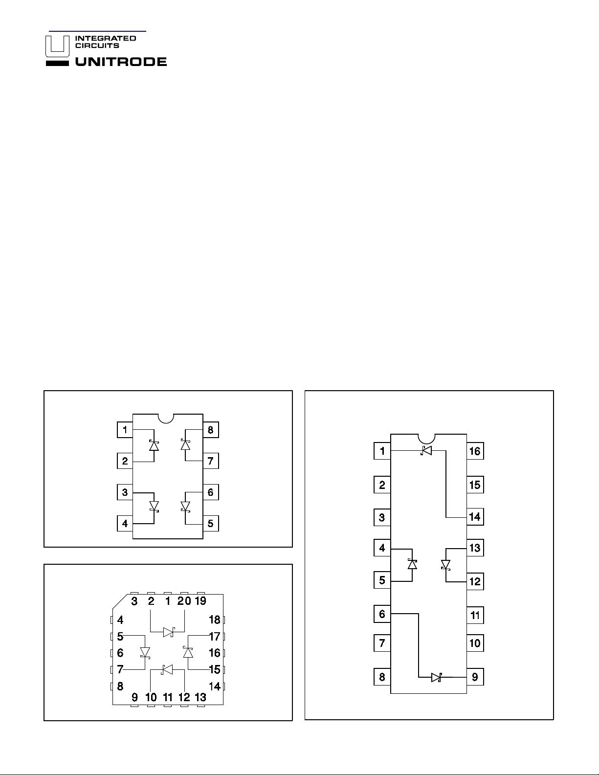
CONNECTION DIAGRAM
DIL-8 (TOP VIEW)
N or J Package
SOIC-16 (TOP VIEW )
DW Package
PLCC-20 (TOP VIEW)
Q Package
6/93
ABSOLUTE MAXI MUM RATING S
All specifications apply to each individual diode . TJ = +25°C except as note d.
TA = TJ.
Peak Inverse Voltag e (per Diode). . . . . . . . . . . . . . . . . . . . . . . . . . . . . . . . . 50V
Diode-to-Diode V o ltage. . . . . . . . . . . . . . . . . . . . . . . . . . . . . . . . . . . . . . . . . 80V
Peak Forwar d Curr ent
UC1611. . . . . . . . . . . . . . . . . . . . . . . . . . . . . . . . . . . . . . . . . . . . . . . . . . . . 1A
UC3611. . . . . . . . . . . . . . . . . . . . . . . . . . . . . . . . . . . . . . . . . . . . . . . . . . . . 3A
Power Dissipat ion at T
A = +70°C . . . . . . . . . . . . . . . . . . . . . . . . . . . . . . . . . . 1W
Storage Temperature Rang e . . . . . . . . . . . . . . . . . . . . . . . . . . -65°C to +150° C
Lead Temperature (Solderin g, 10 Sec onds ). . . . . . . . . . . . . . . . . . . . . . . +300°C
Note: Please consult Packaging Sectio n of Data book for thermal l imitat ions and
considerations of pac kage .
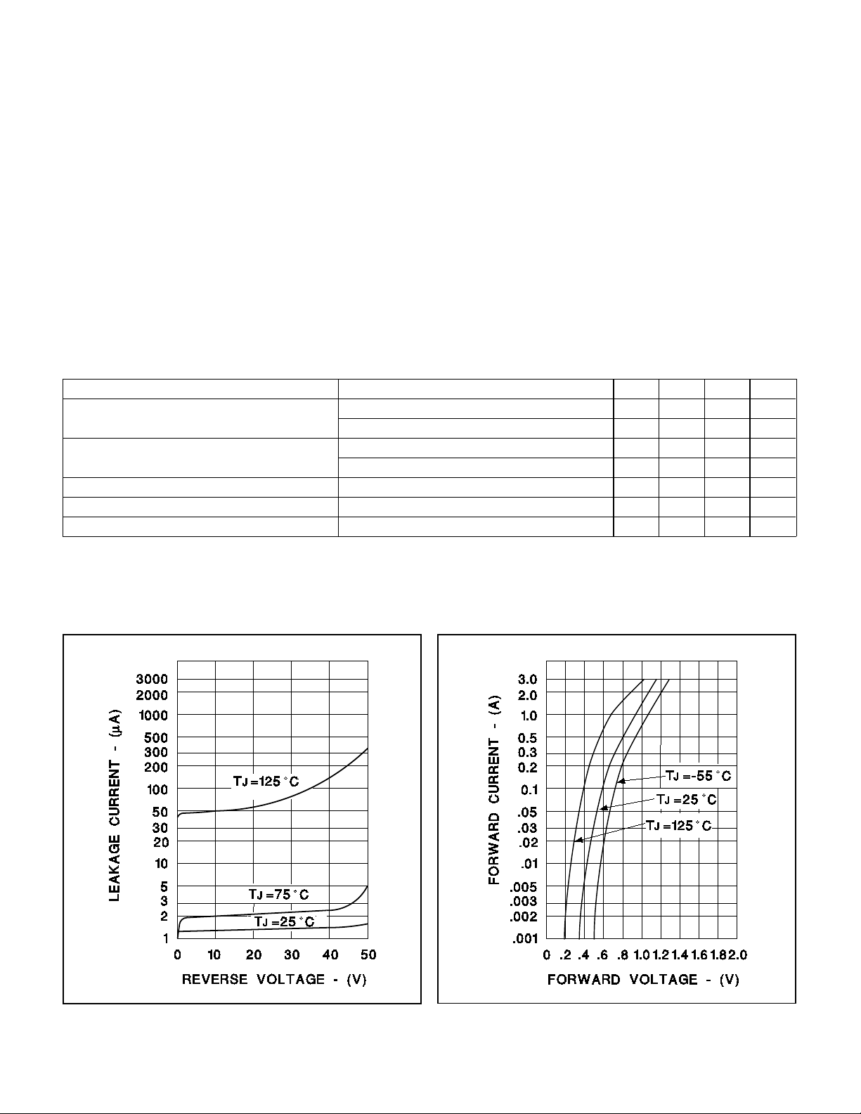
ELECTRICAL CHARACTERISTICS:
PARAMETER TEST CONDITIONS MIN. TYP. MAX. UNITS
Forward Voltage Dro p I
Leakage Current V
Reverse Recovery 0.5A Forward to 0.5A Revers e 20 ns
Forward Recovery 1A Forward to 1.1V Recovery 40 ns
Junction Capacitance V
F = 100mA 0.3 0.4 0.7 V
I
F = 1A 0.9 1.2 V
R = 40V 0.01 0.1 mA
V
R = 40V, TJ = +100°C 0.1 1.0 mA
R = 5V 100 pF
UC1611
UC3611
Note: At Forward current s of gr eat er tha n 1.0A, a para sitic cu rrent of appr oxim at ely 10m A m ay be colle ct ed by adja cent diode s.
Reverse Current vs V oltage Forward Curren t vs Voltage
2
 Loading...