

Texas Instruments UCC3911DP-2, UCC3911DPTR-4, UCC3911DPTR-3, UCC3911DPTR-2, UCC3911DPTR-1 Datasheet
UCC3911 -1/-2/-3/-4
PRELIMINARY
SLUS429 - DECEMBER 1999
FEATURES
•
Protects Sensitive Lithium-Ion
Cells from Overcharging and
Over-Discharging
•
Used for Two-Cell Lithium-Ion
Battery Packs
•
No External FETs Required
•
Provides Protection Against
Battery Pack Output Short
Circuit
•
Extremely Low Power Drain
on Batteries of About 20µA
•
Low Internal FET Switch
Voltage Drop
•
User Controllable Delay for
Tripping Short Circuit Current
Protector
• 3A Current Capacity
Lithium-Ion Battery Protector
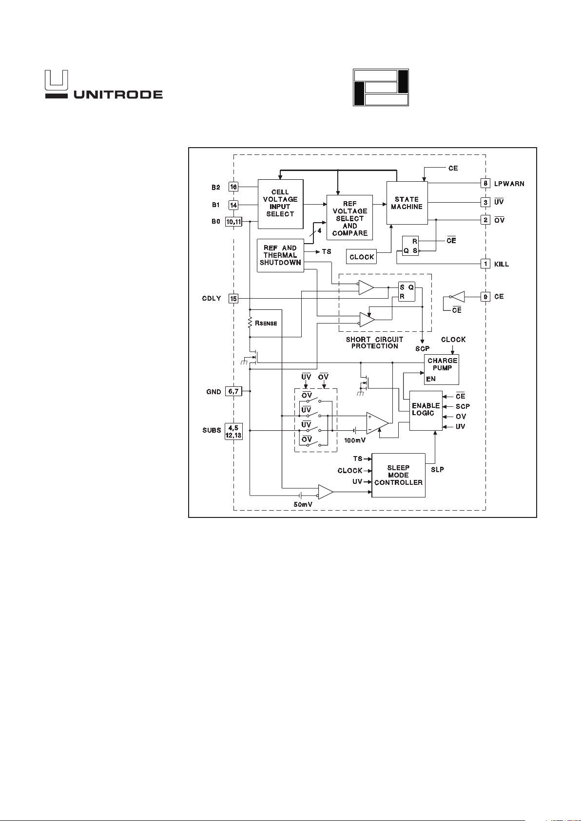
BLOCK DIAGRAM
UDG-95130-2
The UCC3911 is a two-cell lithium-ion battery pack pro
tector IC that incorporates an on-chip series FET switch
thus reducing manufacturing costs and increasing reli
ability. The IC’s primary function is to protect both lith
ium-ion cells in a two-cell battery pack from being either
overcharged or over-discharged. It employs a precision
bandgap voltage reference that is used to detect when
either cell is approaching an overcharged or
over-discharged state. When on board logic detects ei
ther condition, the series FET switch opens to protect the
cells.
A negative feedback loop controls the FET switch when
the battery pack is in either the overcharged or
over-discharged state. In the overcharged state the ac
tion of the feedback loop is to allow only discharge cur
rent to pass through the FET switch. In the
over-discharged state, only charging current is allowed to
flow. The op amp that drives the loop is powered only
when in one of these two states. In the over-discharged
state the chip enters sleep mode until it senses that the
pack is being charged.
The FET switch is driven by a charge pump when the
battery pack is in a normally charged state to achieve the
lowest possible RDS
ON. In this state the negative feed
back loop’s op amp is powered down to conserve battery
power. Short circuit protection for the battery pack is pro
vided and has a nominal delay of 100µs before tripping.
An external capacitor may be connected between CDLY
and B0 to increase this delay time to allow longer
overcurrent transients.
A chip enable (CE) pin is provided that while held low, in
hibits normal operation of the chip to facilitate assembly
of the battery pack.
The UCC3911 is specified for operation over the temper
ature range of −20°C to +70°C, the typical operating and
storage temperature range of lithium-ion batteries.
DESCRIPTION
application
INFO
available
2
UCC3911 -1/-2/-3/-4
ELECTRICAL CHARACTERISTICS:
Unless otherwise specified, these specifications apply for –20°C to +70°C for the
UCC3911, all voltages are referenced to B0, V
B2
= 7.2V, TA=TJ.
PARAMETER TEST CONDITIONS MIN TYP MAX UNITS
State Transition Threshold
Normal to Overcharge UCC3911-1 4.15 4.2 4.25 V
Overcharge to Normal 3.6 3.7 3.8 V
Normal to Overcharge UCC3911-2 4.2 4.25 4.3 V
Overcharge to Normal 3.65 3.75 3.85 V
Normal to Overcharge UCC3911-3 4.25 4.3 4.35 V
Overcharge to Normal 3.7 3.8 3.9 V
Normal to Overcharge UCC3911-4 4.3 4.35 4.4 V
Overcharge to Normal 3.75 3.85 3.95 V
Normal to Undercharge 2.42 2.5 2.58 V
Undercharge to Normal 2.90 3.0 3.10 V
B0/GND Switch
V
B0-VGND
(Normal) IGND = 2A –320 –160 mV
(Normal) I
GND = –2A 160 320 mV
(Overcharge) I
GND = 1mA –300 –150 mV
(Overcharge) I
GND = 2A –500 –250 mV
(Undercharge) I
GND = –1mA 150 300 mV
(Undercharge) I
GND = –2A 250 500 mV
I
GND (Overcharge) VGND = –5V –5 µA
(Undercharge) V
GND = 5V 0 30 µA
Chip Bias Current
I
B2 Nominal 18 25 µA
I
B2 In Sleep Mode 3.5 µA
I
B1 –1 0 1 µA
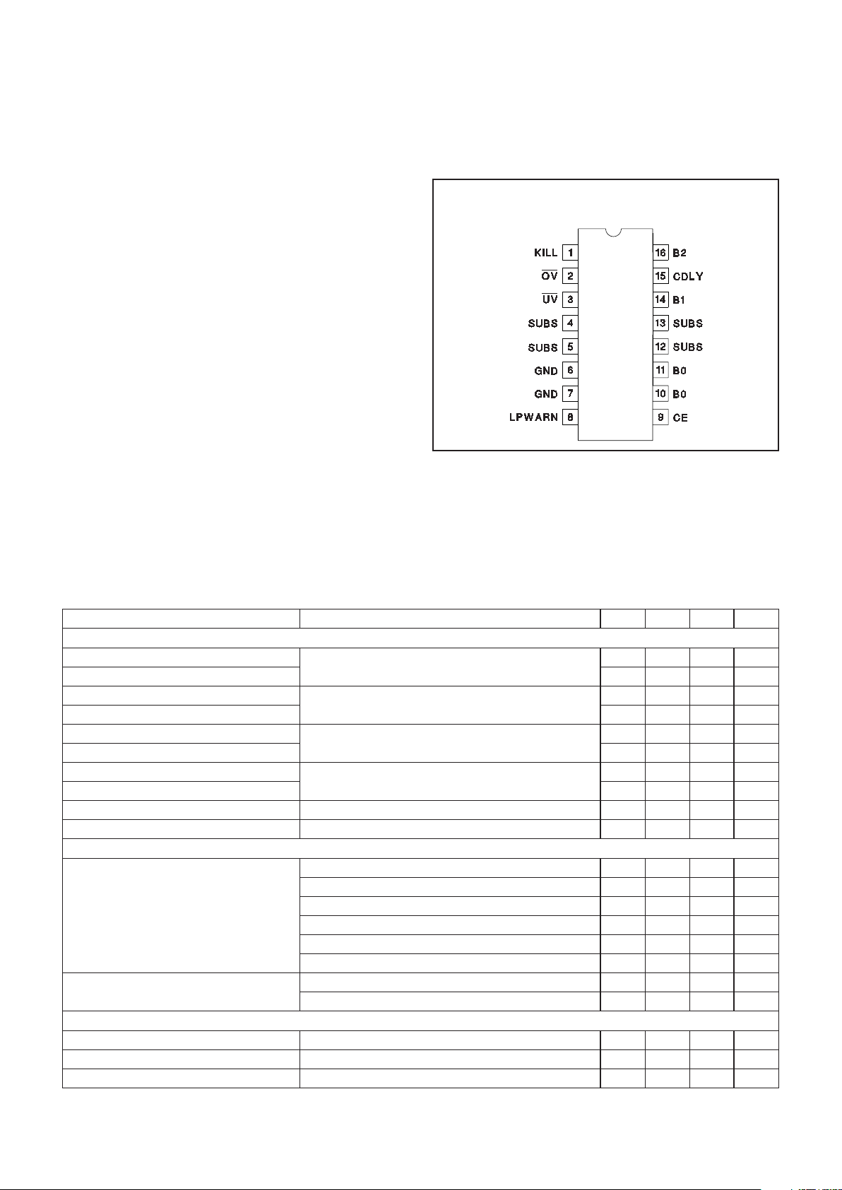
CONNECTION DIAGRAM
SOIC-16 (Top View)
DP Package
ABSOLUTE MAXIMUM RATINGS
Maximum Input Voltage (B2, GND) . . . . . . . . . . . . . . . . . . . 14V
Minimum Input Voltage (B0, GND) . . . . . . . . . . . . . . . . . . −9.0V
Maximum Charge Current (B0, GND) . . . . . . . . . . . . . . . . 3.3A
Minimum Discharge Current (B0, GND) . . . . . . . . . . . . . . . 3.3A
Storage Temperature . . . . . . . . . . . . . . . . . . . −65°C to +150°C
Junction Temperature. . . . . . . . . . . . . . . . . . . –55°C to +150°C
Lead Temperature (Soldering, 10 sec.) . . . . . . . . . . . . . +300°C
Currents are positive into, negative out of the specified terminal.
Consult Packaging Section of Databook for thermal limitations
and considerations of packages.

3
UCC3911 -1/-2/-3/-4
ELECTRICAL CHARACTERISTICS:
Unless otherwise specified, these specifications apply for –20°C to +70°C for the
UCC3911, all voltages are referenced to B0, V
B2
= 7.2V, TA=TJ.
PARAMETER TEST CONDITIONS MIN TYP MAX UNITS
Short Circuit Protection
I
THRESHOLD 3.5 5.25 7 A
T
DLY CDLY = Open (Note 1) 100 µs
Internal Clock Frequency (Note 2) 7.5 kHz
T
DLY -OV Delay for Chip to Register OV Condition 0.6 2 5 ms
T
DLY -UV Delay for Chip to Register UV Condition 0.3 1 3.5 ms
OV
,UV Output Characteristics VB2 -VHIGH with IPIN = –100µA 0.15 0.50 V
V
LOW With IPIN = 100µA 0.05 0.43 V
Thermal Shutdown (Note 1) 165 °C
KILL Output Characteristics V
B2 -VHIGH With IKILL = –0.5mA 0.075 0.290 V
KILL Output Characteristics V
LOW With IKILL = 0.5mA 0.05 0.27 V
LPWARN Output Characteristics V
B2 -VHIGH With ILPWARN = –0.1mA 0.05 0.42 V
V
LOW With ILPWARN = 0.1mA 0.04 0.37 V
CE Threshold Voltage V
B2 = 8.5V 5 6 7 V
V
DD = 5V 2.05 2.45 4.05 V
Note 1: Guaranteed by design. Not 100% tested in production.
Note 2: Tested at functional probe only.
PIN DESCRIPTIONS
B0: Connects to the negative terminal of the lower cell
in the battery pack.
B1: Connects to the junction of the positive terminal of
the lower cell and the negative terminal of the upper cell
in the battery pack.
B2: Connects to the positive terminal of the upper cell in
the battery pack. This pin also connects to the positive of
the two terminals that are presented to the user of the
battery pack.
CDLY: Delay control pin for the short circuit protection
feature. A capacitor connected between this pin and the
B0 pin will lengthen the time delay from when an
overcurrent situation is detected to when the protection
circuitry is activated. This control will be useful for those
applications where high peak load currents may
momentarily exceed the protection circuit’s threshold
current and interruption of the battery current would be
undesirable. The nominal delay time is internally set at
100µs. The equation for determining this delay is:
T
DLY (µs) = 25 + (25 + CDLY (pF)) • 0.4 • VB2
To recover from an overcurrent “shutdown” the load must
be removed momentarily from the pack.
CE: Chip Enable. While this signal is held low, the
internal FET is held off and the KILL latch is held in
reset. CE is pulled high by a 2µA current source. This
function was included to facilitate construction of the
battery pack by preventing the KILL latch from being
erroneously set during final assembly. The last step in
the electrical assembly of the pack would be cutting a
link to B0.
GND: The second of the two terminals that are
presented to the user of the battery pack. The internal
FET switch connects this terminal to the B0 terminal to
give the battery pack user appropriate access to the
batteries. In an overcharged state, current is allowed to
flow only into this terminal. Similarly, in an
over-discharged state, current is allowed to flow only out
of this terminal.
KILL: This active-high signal indicates that one or both
of the cells has been overcharged. It can be used to
drive a circuit breaker of some sort to permanently
disable the battery pack as a safety feature. Note that
when KILL goes active the chip simultaneously enters
the OV
state which inhibits further charging of the pack.
The KILL latch is asynchronously reset by the CE signal.

4
UCC3911 -1/-2/-3/-4
1
3
2
4
5
7
6
8
16
14
15
13
12
10
11
9
KILL
OV
UV
SUBS
SUBS
GND
LPWARN
GND
B2
CDLY
B1
SUBS
SUBS
B0
CE
B0
UCC3911
J1
ISOLATED COPPER PAD
FOR HEAT SINKING AT
HIGH LOAD CURRENTS
C2
0.22µF
R1 10k
+
CELL 1
ENABLE (OPEN)
C
DLY
330pF
C1 10µF
10V
R1 220Ω
+
CELL 2
C4
(OPTIONAL)
ISOLATED
COPPER PAD
FOR HEAT
SINKING AT
HIGH LOAD
CURRENTS
C3
0.1µF
25V
PACK+
PACK–
LOW POWER WARN
(ACTIVE HIGH)
+
APPLICATION INFORMATION
Figure 1. UCC3911 Application circuit including components for short circuit protection.
UDG-99173
Note: In this example, CDLY, C1 and C2 were selected to drive a 1500µF load.
LPWARN: This active-high signal is the low Power
Warning. The voltage on this pin goes high (to B2
potential) as soon as either of the battery’s cells voltage
falls below 3.0V. Once the UV
state is entered, this
output goes back to low.
OV:
This active-low signal indicates the state of the state
machine’sOV
bit. When low, it indicates that one or both
cells are overcharged. Further charging is inhibited by
the opening of the FET switch. The internal signal also
sets the KILL latch and activates the KILL output signal.
The output buffer for this pin is sized to drive a very light
load.
SUBS: The substrate connections for the UCC3911.
Connect these points to a heat sink which is electrically
isolated from all other IC pins.
UV:
This active-low signal indicates the state of the state
machine’sUV
bit. When low, it indicates that one or both
cells are over- discharged. Further discharging is
inhibited by the opening of the FET switch. The chip
enters the “Sleep” mode when UV
goes high and waits in
this state until the chip detects that the battery pack has
been placed in a charging circuit. The output buffer for
this pin is likewise sized to drive a very light load.
Figure 1 shows a typical application for the UCC3911 lith
ium-ion battery protector. All of the functions required to
protect two series lithium-ion cells from overcharge and
over-discharge, as well as provide short circuit protection,
are included in a single chip. An internal state machine
controls an internal power FET which allows either
bi-directional or uni-directional battery current. An optional
time delay capacitor can be included to slow the reac
-
tion time of the short circuit protection circuitry if desired.
While the IC is capable of providing overload and
over/undervoltage protection of both cells with virtually
no external parts, the demands of true short circuit pro
-
tection require some passive external components.

5
UCC3911 -1/-2/-3/-4
State Machine Operation
The internal state machine constantly monitors the two
cells for both overvoltage and undervoltage conditions.
Figure 2 shows a state diagram which describes the oper
ation of the protection circuitry. In the normal mode, both
the OV
and UV status bits are held high and full battery
current is allowed through the internal power FET in ei
ther the charge or discharge direction.
If the voltage across one or both cells exceeds 4.25V, the
OV
signal goes low, and further charge current is not al
lowed. An internal feedback loop controls the power FET
to allow only discharge current, allowing for battery recov
ery. The state machine will not reenter normal mode until
the voltage across both cells decays to less than 3.75V.
This feature is important to prevent circuit oscillation due
to battery ESR when the circuitry transitions between
states. The KILL output signal is also set high when the
UCC3911 enters the OV state, and will remain set unless
the CE pin is brought low. The KILL latch can be used to
permanently disable the battery pack with additional cir
cuitry if desired.
If the voltage across one or both battery cells falls below
3V, the LPWARN signal goes high indicating a low power
condition. This signal can be used to signal the user that
the battery pack is in need of charge.
If the voltage across one or both cells falls below 2.5V,
the UV
signal goes low, and the feedback loop allows
only charge current. The LPWARN signal goes low and
the UCC3911 enters sleep mode which consumes only
3
A, limiting self discharge to a minimum. The circuit re
-
mains in this state until the voltage across both cells ex
ceeds 3V. The battery pack can still be charged, unless
the sum of the two cells voltages falls below 3.7V, which
is the minimum guaranteed operating voltage for the IC.
If the battery cells become so poorly matched that the
voltage across one cell exceeds 4.25V and the voltage
across the other cell falls below 2.5V, the power FET will
not pass either charge or discharge current, and both
the OV
and UV signals will be set low.
The normal high current path for battery current is
through the B0 (10, 11) and GND (6, 7) pins of the
UCC3911. The GND pins are intended to be connected
to system ground for either the charger or the load. The
SUBS pins (4, 5, 12, 13) are internally connected to the
substrate of the UCC3911, which is internally referenced
to B0 or GND depending on the direction of pack current. If high battery currents are anticipated, the SUBS
pins can be thermally connected to a heat sink to control
the IC temperature. However, this heat sink must be
electrically isolated from all other IC pins including
ground. This is a critically important point, as heat sinking to the system ground is not possible.
The CE pin is used to initialize the state of the battery
pack during assembly. Holding this pin low forces the
state machine to hold the FET off. The last step in the
assembly process would be to cut the trace between
this pin and B0 which allows the internal pull up to start
the state machine.
Short Circuit Protection
As stated earlier, the demands of true short circuit pro
tection requires that careful attention be paid to the se
lection of a few external components. This selection is
discussed below.
In the Application circuit of Fig. 1, C3 protects the bat
tery pack output terminals from inductive kick when the
pack current is shut off due to an overcurrent or
over/undervoltage condition. (It also increases the ESD
protection level.)
To prevent a momentary cell voltage drop, caused by
large capacitive loads, from causing an erroneous
undervoltage shutdown, an RC filter is required in series
with the two battery sense inputs, B1 and B2. The resis
tors (R1 and R2) are sized to have a negligible impact
on voltage sensing accuracy. The capacitors (C1 and
APPLICATION INFORMATION (cont.)
Figure 2. State diagram.
UDG-96122
Note: The “One Cell Over and One Cell Under” state is entered whenever one cell is overcharged and the other cell is
simultaneously over-discharged. When in this state, the series FET switch is turned off inhibiting both charging and discharging of the battery pack. If the battery pack ever gets
into this condition, it should be discarded.

6
UCC3911 -1/-2/-3/-4
C2) should be sized to provide a time constant longer
than the overcurrent delay time. In the example of Figure
1, they are sized for a nominal 2.2ms time constant. They
do not need to be low ESR style capacitors, as they see
no ripple current. A larger resistor value and smaller ca
-
pacitor value can be used on the B1 input due to the ex
-
tremely low input current on this pin.
The overcurrent delay capacitor, C
DLY
, sets the time de
lay, after the overcurrent threshold is exceeded, before
turning off the UCC3911’s internal FET. If no capacitor is
used, the nominal delay is 100
s. To charge large capaci
tive loads without tripping the overcurrent circuit, a small
capacitor (typically less than 1000pF) is used to extend
the delay time. The approximate delay time is given be
low and shown graphically in Figure 3.
() ( )
()
ts CpF V
DLY DLY B
µ= + + • •25 25 0 42.
The amount of time required will be a function of the load
capacitance, battery voltage, and the total circuit impedance, including the internal resistance of the cells, the
UCC3911’s on resistance, and the load capacitor ESR.
The required delay time can be calculated from:
tRCn
IR
V
=− • •
•
1
In this equation, R is the total circuit resistance, C is the
capacitor being charged, I is the overcurrent trip current
(5.25A nominal), and V is the battery voltage. Using the
minimum trip current of 3.5A and the maximum battery
voltage of 8.4V, the worst case maximum delay time re
-
quired is defined as:
() ( )
tsRCFn
R
max.µµ=− • • •
1
24
In the example of Figure 1, CDLY, C1 and C2 are sized
to drive a 1500
F load capacitor.
If large capacitive loads (or other loads with surge cur
rents above the overcurrent trip threshold) are not being
applied to the pack terminals, the overcurrent delay time
can be short. In this case, it may be possible to elimi
nate CDLY, as well as R2 and C2 altogether (replacing
R2 with a short). In addition, the time constant of R1 and
C1 can be made much shorter. R1 and C2 are still nec
essary, however, to assure proper operation under short
circuit conditions. It is important to maintain a minimum
R1/C1 time constant of 100
s. (For example, R1 and C1
could be reduced to 100
and 1 F.)
Capacitor C4 is recommended, for the case where the
wires connecting to the top and bottom of the cell stack
are more than an inch long (not likely in a small battery
pack). In this case, a 10
f, low ESR capacitor is recommended to prevent excessive overshoot at turn-off due
to wiring inductance.
APPLICATION INFORMATION (cont.)
0
500
1,000
1,500
2,000
2,500
3,000
3,500
0 200 400 600 800 1,000
DELAY CAP (pF)
DELAY (us)
VB2=8
VB2=7
VB2=6
VB2=5
Figure 3. Nominal overcurrent delay time vs CDLY
and B2 voltage.
UNITRODE CORPORATION
7 CONTINENTAL BOULEVARD • MERRIMACK, NH 03054
TEL (603) 424-2410 ( FAX (603) 424-3460
 Loading...