UCC3830-4/-5/-6
02/99
FEATURES
• 5-Bit Digital-to-Analog Converter
(DAC)
• Supports 4-Bit and 5-Bit
Microprocessor VID Codes
• Combined DAC/Voltage Monitor
and PWM Functions
• 1% DAC/Reference
• Current Sharing
• 100kHz, 200kHz, 400kHz
Oscillator Frequency Options
• Foldback Current Limiting
• Overvoltage and Undervoltage
Fault Windows
• Undervoltage Lockout
• 4Ω Totem Pole Output
• Chip Disable Function
5-Bit Microprocessor Power Supply Controller
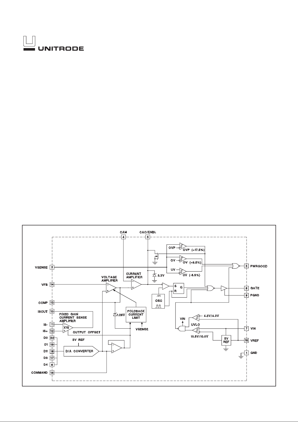
BLOCK DIAGRAM
UDG-96188-2
DESCRIPTION
The UCC3830-4/-5/-6 is a fully integrated single chip solution ideal for powering high performance microprocessors. The chip includes an average current
mode PWM controller, has a fully integrated 5-Bit DAC, and includes an
on-board precision reference and voltage monitor circuitry. The UCC3830-x
converts 5VDC to an adjustable output, ranging from 3.5VDC down to 1.8VDC
with 1% DC system accuracy (see Table 1). The UCC3830-x fully supports
Intel’s 4-bit Pentium® Pro and 5-bit Pentium® II VID codes.
The accuracy of the DAC/reference combination is 1%. The overvoltage and
undervoltage comparators monitor the system output voltage and indicate
when it rises above or falls below its programmed value by more than 8.5%. A
second overvoltage protection comparator pulls the current amplifier output
voltage low to force zero duty cycle when the system output voltage exceeds
its designed value by more than 17.5%. This comparator also terminates the
cycle. Undervoltage lockout circuitry assures the correct logic states at the
outputs during powerup and powerdown. The gate output can be disabled by
bringing the CAO/ENBL pin to below 0.8V.
(continued)

2
UCC3830-4/-5/-6
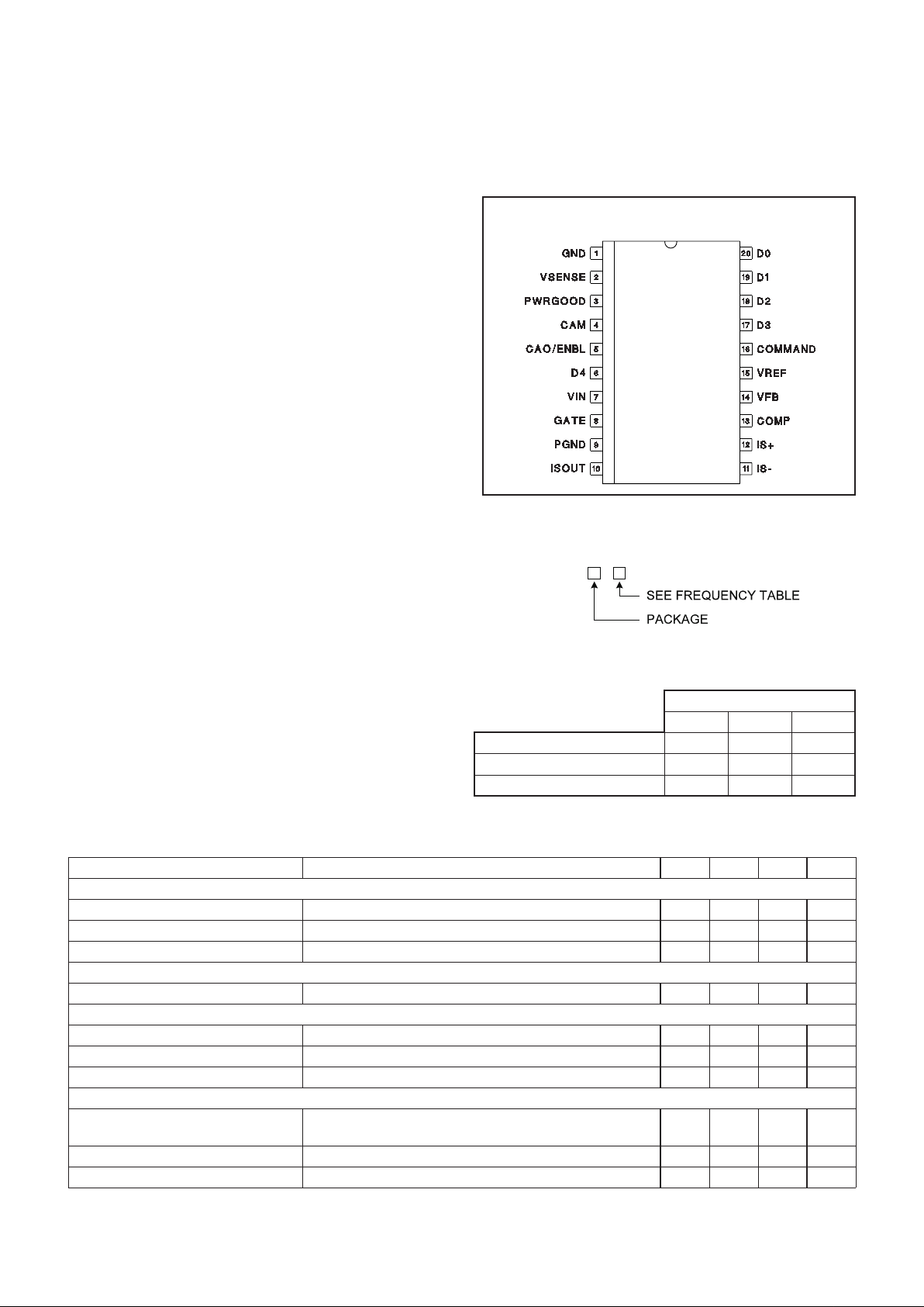
CONNECTION DIAGRAM
SOIC-20 (Top View)
DW Package
ELECTRICAL CHARACTERISTICS:
Unless otherwise specified, VIN = 12V, VSENSE = 3.5V, VD0 = VD1 = VD2 = VD3 =
VD4 = 0V, 0°C < TA < 70°C, TA= TJ.
PARAMETER TEST CONDITIONS MIN TYP MAX UNITS
Undervoltage Lockout
VIN UVLO Turn-on Threshold 10.5 10.8 V
VIN UVLO Turn-off Threshold 9.5 10 V
UVLO Threshold Hysteresis 200 500 700 mV
Supply Current
l
IN D0 through D4 = Open 7.5 13.5 mA
DAC/Reference
COMMAND Voltage Accuracy 10.8V < VIN < 13.2V, I
VREF
= 0mA, 0°C < TA < 70°C –1 1 %
D0-D4 Voltage High DX Pin Floating 4 5 5.2 V
D0-D4 Input Bias Current DX Pin Tied to GND –100 –70 –20 µA
OVP Comparator
Trip Point % Over COMMAND Voltage (Note 1), D0 = D1 = D2 = D4
= Open, D3 = GND
10 17.5 25 %
Hysteresis 20 30 mV
VSENSE Input Bias Current OV, OVP, UV Combined –0.5 –0.1 0.5 µA
The voltage and current amplifiers have a 3MHz gain
bandwidth product to satisfy high performance system
requirements. The internal current sense amplifier permits the use of a low value current sense resistor, minimizing power loss. The oscillator frequency is fixed
internally at 100kHz, 200kHz, or 400kHz, depending
upon the option selected. The foldback circuit reduces
the converter short circuit current limit to 50% of its nominal value when the converter is short circuited. The gate
driver is a 4Ω totem pole output stage capable of driving
an external MOSFET.
This device is available in 20-pin dual in-line and surface
mount packages. The UCC3830-x is specified for operation from 0°C to 70°C.
Pentium®Pro and Pentium®Pro II are registered trademarks of
Intel Corporation.
DESCRIPTION (cont.)
FREQUENCY TABLE
Frequency
100kHz 200kHz 400kHz
UCC3830-4 X
UCC3830-5 X
UCC3830-6 X
UCC3830 –
ORDERING INFORMATION
Note: Consult factory for temperature range or package op-
tions not shown.
ABSOLUTE MAXIMUM RATING
Input Supply Voltage VIN . . . . . . . . . . . . . . . . . . . . . . . . . . 15V
D0, D1, D2, D3, D4, VSENSE, VFB, IS+, IS–, CAM Inputs
Maximum Forced Voltage. . . . . . . . . . . . . . . . –0.3V to 5.3V
PWRGOOD Output Maximum Voltage. . . . . . . . . . . . . . . . 5.5V
COMMAND Ouput Maximum Current . . . . . . Internally Limited
Reference Output Current . . . . . . . . . . . . . . . Internally Limited
Storage Temperature . . . . . . . . . . . . . . . . . . . –65°C to +150°C
Junction Temperature. . . . . . . . . . . . . . . . . . . –55°C to +150°C
Lead Temperature (Soldering, 10 sec.). . . . . . . . . . . . . +300°C
Currents are positive into negative out of the specified terminal.
Pulse is defined as a less than 10% duty cycle with a maximum
duration of 500 s. Consult Packaging Section of Databook for
thermal limitations and considerations of packages.

3
UCC3830-4/-5/-6
ELECTRICAL CHARACTERISTICS: Unless otherwise specified, VIN = 12V, VSENSE = 3.5V, VD0 = VD1 = VD2 = VD3 =
VD4 = 0V, 0°C < TA < 70°C, TA= TJ.
PARAMETER TEST CONDITIONS MIN TYP MAX UNITS
OV Comparator
Trip Point % Over COMMAND Voltage (Note 1), D0 = D1 = D2 = D4
= Open, D3 = GND
5 8.5 12 %
Hysteresis 20 30 mV
PWRGOOD Equivalent Resistance VSENSE = 2.0V 470 Ω
UV Comparator
Trip Point % Over COMMAND Voltage (Note 1), D0 = D1 = D2 = D4
= Open, D3 = GND
–12 –8.5 –5 %
Hysteresis 20 30 mV
Voltage Error Amplifier
Input Bias Current V
CM = 3.0V –0.5 –0.02 0.5 µA
Open Loop Gain 1.5V < V
COMP
< 2.5V, D4 = D3 = D2 = D1 = GND, D0 =
Open
80 dB
Power Supply Rejection Ratio 10.8V < VIN < 15V 85 dB
Output Sourcing Current V
VFB = 2V, VCOMMAND = VCOMP = 2.5V –0.5 –0.3 mA
Output Sinking Current V
VFB = 3V, VCOMMAND = VCOMP = 2.5V 0.5 1 mA
Current Sense Amplifier
Gain 14.25 15.25 V/V
Input Resistance 3kΩ
Common Mode Rejection Ratio 0V < V
CM < 4.5V 60 dB
Power Supply Rejection Ratio 10.8V < VIN < 15V 80 dB
Output Sourcing Current V
IS– = 2V, VISOUT = VIS+ = 2.5V –0.5 –0.3 mA
Output Sinking Current V
IS– = 3V, VISOUT = VIS+ = 2.5V 5 8 mA
Current Amplifier
Input Offset Voltage V
CM = 3.0V –12 12 mV
Input Bias Current V
CM = 3.0V –0.1 µA
Open Loop Gain 1V < V
CAO/ENBL < 2.5V 80 dB
Output Voltage High V
COMP = 3V, VCAM = 2.5V 3.2 V
Power Supply Rejection Ratio 10.8V < VIN < 15V 80 dB
Output Sourcing Current V
CAM = 2V, VCAO/ENBL = VCOMP = 2.5V –1 –0.5 mA
Output Sinking Current V
CAM = 3V, VCAO/ENBL = VCOMP = 2.5V 3 5 mA
Oscillator
Frequency (-4) 85 100 115 kHz
Frequency (-5) 170 200 230 kHz
Frequency (-6) 340 400 460 kHz
Frequency Change With Voltage 10.8V < VIN < 15V 1 %
Output Section
Maximum Duty Cycle 90 95 99 %
Output Low Voltage I
GATE = –100mA 0.2 V
Output High Voltage I
GATE = 100mA 11.8 V
Rise Time C
GATE = 3.3nF 20 70 ns
Fall Time C
GATE = 3.3nF 15 70 ns
Foldback Current Limit
Clamp Level Measured at Voltage EA Output;
V
SENSE = VCOMMAND = 3V
4.28 V
V
COMMAND = 3V, VSENSE = 0 3.64 V
Note 1: This percentage is measured with respect to the ideal COMMAND voltage programmed by the D0 - D4 pins.
 Loading...