UCC2585
UCC3585
PRELIMINARY
DESCRIPTION
The UCC2585/UCC3585 synchronous Buck controller provides flexible
high efficiency power conversion for output voltages as low as 1.25V with
guaranteed ±1% DC accuracy. Output currents are only limited by the
choice of external logic level MOSFETs. With an input voltage range of
2.5V to 6.0V it is the ideal choice for 3.3V only, battery input, or other low
voltage systems. Applications include local microprocessor core voltage
power supplies for desktop and Notebook computers, and high speed GTL
bus regulation.Its fixed frequency oscillator is capable of providing practical
PWM operation to 700kHz.
With its low voltage capability and inherent “always on” operation, the
UCC2585/UCC3585 causes VOUT to track VIN once VIN has exceeded
the threshold voltage of the external P channel MOSFET. Tracking can be
tailored for any application with a single resistor or disabled by connecting
TRACK to VIN. For dual supply rail microprocessors this feature negates
the need for external diodes to insure supply voltage tracking between the
+3.3V and lower voltage microprocessor core supplies.
(continued)
Low Voltage Synchronous Buck Controller
FEATURES
•
Resistor Programmable 1.25V to 4.5V
V
OUT
•
2.5V to 6V Input Supply Range
•
1% DC Accuracy
•
High Efficiency Synchronous
Switching
•
Drives P-channel (High Side) and
N-channel (Low Side) MOSFETs
•
Lossless Programmable Current Limit
•
Logic Compatible Shutdown
•
Programmable Frequency
•
Start-up Voltage Tracking Protects
Dual Rail Microprocessors
07/99
12
14
6
11
8
PDRV
CLSET
ISENSE
13
5
9
NDRV
PWRGND
TRACK
N/C
1
4
10
2
15 VIN
VFB
ENB
COMP
SD
16
7
3 SS
GND
CT
ISET
C8
0.47µF
Q1
IRF7404
Q2
IRF7401
L1 4.7µF
C9
220µF
C10
220µF
C11
VOUT
RTN
RTN
VIN
220µF
+
++
R4
100k
R2
549k
R6
3
R5
3
R1
10k
R3
27.4k
R12
32k
R10
36k
R11
82k
C6
470pF
C5
0.22µF
C4
3.2N
C7
147pF
C1
150µFC2150µF
++
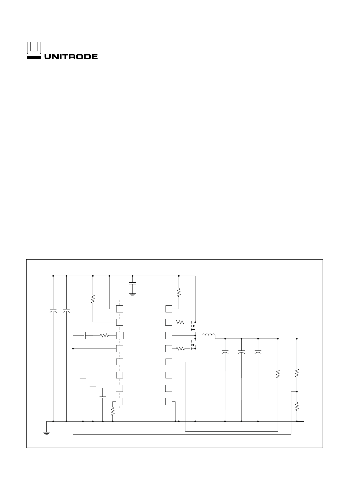
TYPICAL APPLICATION DIAGRAM
UDG-98024

2
UCC2585
UCC3585
DIL-16, SOIC-16, SSOP-16 (TOP VIEW)
J, N, D, and M Packages
ABSOLUTE MAXIMUM RATINGS
Analog Pins
Minimum and Maximum Forced Voltage
(Reference to GND) . . . . . . . . . . . . . . . . . . . –0.3V to +6.3V
Digital Pins
Minimum and Maximum Forced Voltage
(Reference to GND) . . . . . . . . . . . . . . . . . . . . .–0.3V to 6.3V
Power Driver Output Pins
Maximum forced current . . . . . . . . . . . . . . . . . . . . . . . . . ±1.0A
Operating Junction Temperature. . . . . . . . . . –55°C to +125°C
Storage Temperature. . . . . . . . . . . . . . . . . . . –65°C to +150°C
Note: Unless otherwise indicated, voltages are reference to
ground and currents are positive into, negative out of, the spec
ified terminals. Pulsed is defined as a less than 10% duty cycle
with a maximum duration of 500ns.
NDRV
VIN
CT
PWRGND
PDRV
SD
ISENSE
N/C
1
2
3
4
5
6
7
8
16
15
14
13
12
11
10
9
COMP
ENB
CLSET
TRACK
ISET
SS
VFB
GND
CONNECTION DIAGRAMS
DESCRIPTION (cont.)
The UCC2585/UCC3585 drives a complementary pair of
power MOSFET transistors, P-channel on the high side,
and N-channel on the low side to step down the input
voltage at up to 90% efficiency.
A programmable two-level current limiting function is provided by sensing the voltage drop across the high side P
channel MOSFET. This circuit can be configured to pro
-
vide pulse-by-pulse limiting, timed shutdown after 7 con
-
secutive faults, or latch-off after fault detection, allowing
maximum application flexibility. The current limit threshold is programmed with a single resistor selected to
match system MOSFET characteristics.
The UCC2585/UCC3585 also includes undervoltage
lockout, a logic controlled enable, and softstart functions.
The UCC2585/UCC3585 is offered in the 16 pin surface
mount and through hole packages.
APPLICATIONS
•
Low Voltage Microprocessor Power such as PowerPC
603 and 604
•
High Power 5V or 3.3V to 1.25V–4.5V Regulators
• GTL Bus Termination

3
UCC2585
UCC3585
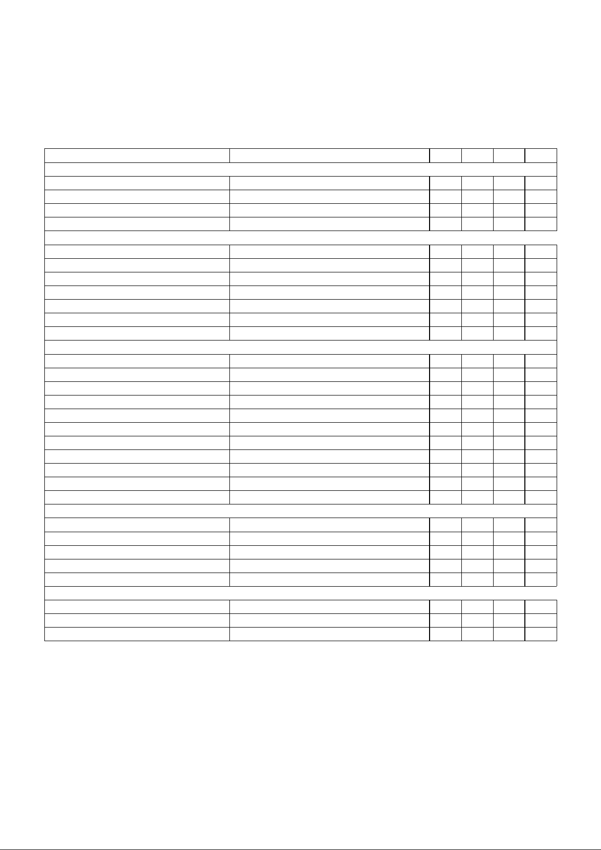
ELECTRICAL CHARACTERISTICS:
Unless otherwise stated, these specifications hold for TA= 0°C to 70°C for the
UCC3585, and T
A
= –40°C to 85°C for the UCC2585. TA=TJ. VIN = 3.3V, ENB, I
SENSE
= VIN,VFB= 1.25V, COMP = 1.5V,
C
T
= 330pF, R
ISET
= 100k, RTRACK = 10k, RCLSET = 10k.
PARAMETER TEST CONDITIONS MIN TYP MAX UNITS
Input Supply Section
Supply Current – Total (Active) 2.3 3.5 mA
Supply Current – Shutdown ENABLE = 0V 10 25 µA
VIN Turn On Threshold (UVLO) 2.35 2.60 V
VIN Turn On Hysteresis 450 550 mV
Voltage Amplifier Section
Input Voltage (Internal Reference) T
A
= 0°C to 70°C, VIN = 3.0V to 3.6V, Note 1 1.238 1.250 1.262 V
Input Voltage (Internal Reference) VIN = 3.0V to 3.6V, IND/MIL Temp, Note 1 1.228 1.250 1.273 V
Open Loop Gain COMP = 0.5 to 2.5V 65 80 dB
Output Voltage High I(COMP) = –50µA 3.00 3.25 V
Output Voltage Low I(COMP) = 50µA 0.10 0.25 V
Output Source Current –100 –175 µA
Output Sink Current 0.4 1.0 mA
Oscillator/PWM Section
Initial Accuracy T
J
= 25°C 405 450 495 kHz
Initial Accuracy Over Temperature 390 450 510 kHz
CT Ramp Peak to Valley 1.8 2.1 2.4 V
CT Ramp Valley Voltage 0.3 0.4 V
PWM Maximum Duty Cycle COMP = 3V, Measured on PDRV 100 %
PWM Minimum Duty Cycle COMP = 0.2V, Measured on PDRV 0 %
PWM Delay to Outputs COMP = 2.5V 45 ns
Tracking Current Measured on TRACK, V
TRACK
= 1.6V 10 12 15 µA
Enable High Threshold Measured on ENABLE (Note 3) 2.8 V
Enable Low Threshold Measured on ENABLE 0.5 V
Softstart Charge Current SS = 0V –10 –14 –18 µA
Current Limit Section
Pulse to Pulse Threshold Measured Between V
IN
and I
SENSE
100 125 150 mV
CLSET Current 11 14 16 µA
SD Sink Current SD = 2V 8 13 18 µA
SD Source Current SD = 2V –100 –140 µA
Restart Threshold Measured on SDOWN 0.40 0.55 0.90 V
Output Driver Section (PDRV, NDRV)
Pull Up Resistance –100mA (Source) T
A
= 25°C6Ω
Pull Down Resistance 100mA (Sink) T
A
= 25°C4Ω
Deadtime Delay Note 2 150 200 250 ns
Note 1. Measured on COMP with the Error Amp in a Unity Gain (voltage follower) configuration.
Note 2. 50% point of PDRV Rise to NDRV Rise and 50% point of NDRV Fall to PDRV Fall.
Note 3. Enable High Threshold = V
IN
–0.5.
 Loading...