SLUS403A - FEBRUARY 2000
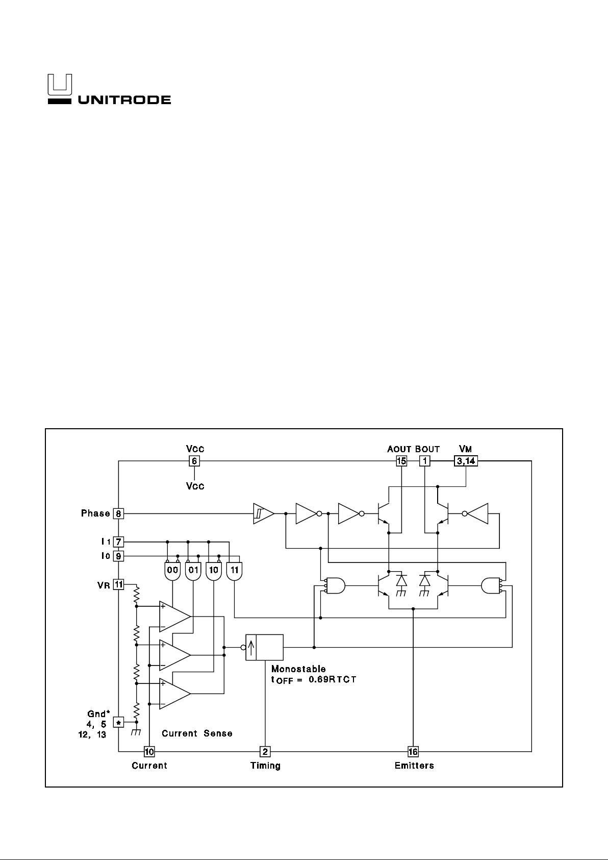
BLOCK DIAGRAM
•
Full-Step, Half-Step and Micro-Step
Capability.
•
Bipolar Output Current up to 2A.
•
Wide Range of Motor Supply Voltage:
10–50V
•
Low Saturation Voltage
•
Wide Range of Current Control: 5mA–2A.
•
Current Levels Selected in Steps or Varied
Continuously.
•
Thermal Protection and Soft Intervention.
The UC3770A and UC3770B are high-performance full bridge driv
ers that offer higher current and lower saturation voltage than the
UC3717 and the UC3770. Included in these devices are LS-TTL
compatible logic inputs, current sense, monostable, thermal shut
down, and a power H-bridge output stage. Two UC3770As or
UC3770Bs and a few external components form a complete micro
processor-controllable stepper motor power system.
Unlike the UC3717, the UC3770A and the UC3770B require exter
nal high-side clamp diodes. The UC3770A and UC3770B are
identical in all regards except for the current sense thresholds.
Thresholds for the UC3770A are identical to those of the older
UC3717 permitting drop-in replacement in applications where
high-side diodes are not required. Thresholds for the UC3770B are
tailored for half stepping applications where 50%, 71%, and 100%
current levels are desirable.
The UC3770A and UC3770B are specified for operation from 0°C
to 70°C ambient.
UC3770A
UC3770B
High Performance Stepper Motor Drive Circuit
FEATURES
DESCRIPTION
UDG-92039-1

2
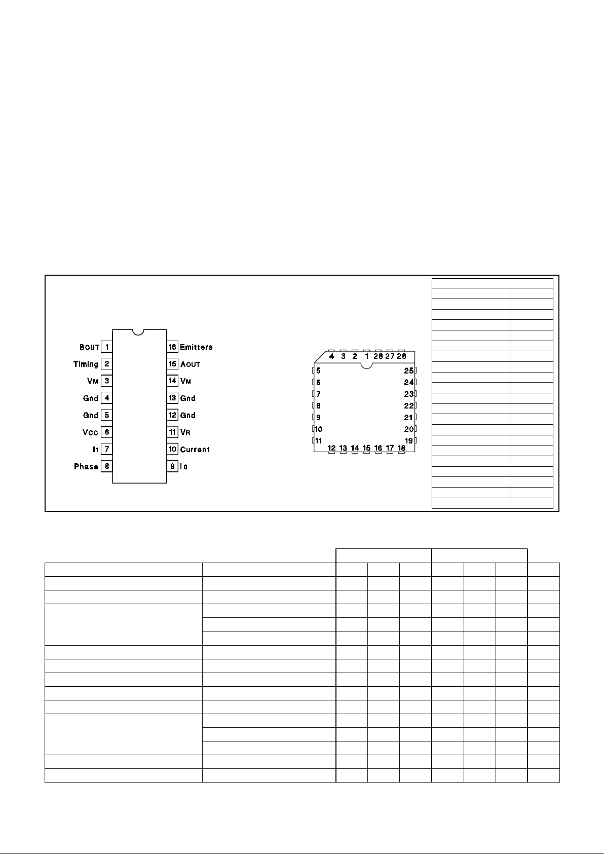
CONNECTION DIAGRAMS
UC3770A
UC3770B
UC3770A UC3770B
PARAMETER TEST CONDITIONS MIN TYP MAX MIN TYP MAX UNITS
Supply Voltage V
M (Pins 3, 14) 10 45 10 45 V
Logic Supply Voltage V
CC (Pin 6) 4.75 5 5.3 4.75 5 5.3 V
Logic Supply Current I
CC (Pin 6) IO = I1 = H, IM = 0 15 25 15 25 mA
I
O = I1 = L, IM = 0 18 28 18 28 mA
I
O = I1 = H, IM = 1.3A 33 40 33 40 mA
Thermal Shutdown Temperature +170 +170 °C
Logic Threshold (Pins 7, 8, 9) 0.8 2.0 0.8 2.0 V
Input Current Low (Pin 8) V
I = 0.4V -100 -100 µA
Input Current Low (Pins 7, 9) V
I = 0.4V -400 -400 µA
Input Current High (Pins 7, 8, 9) V
I = 2.4V 10 10 µA
Comparator Threshold (Pin 10) V
R = 5V, I0 = L, I1 = L 400 415 430 400 415 430 mV
V
R = 5V, I0 = H, I1 = L 240 255 265 290 300 315 mV
V
R = 5V, I0 = L, I1 = H 70 80 90 195 210 225 mV
Comparator Input Current (Pin 10) ±20 ±20 µA
Off Time R
T = 56k, CT = 820pF 25 30 35 25 30 35 ms
PACKAGE PIN FUNCTION
FUNCTION PIN
Gnd 1-3
V
M 4
N/C 5
A
OUT 6
N/C 7
Emitters 8
Gnd 9
B
OUT 10
Timing 11
V
M 12
Gnd 13-17
V
CC 18
I
1 19
Phase 20
I
0 21
N/C 22
Current 23
V
R 24
N/C 25-27
Gnd 28
PLCC-28 (Top View)
Q Package
DIL-16 (Top View)
J Or N Package
Logic Supply Voltage, VCC . . . . . . . . . . . . . . . . . . . . . . . . . . . . . . . . . . . . . . . . . 7V
Output Supply Voltage, VMM. . . . . . . . . . . . . . . . . . . . . . . . . . . . . . . . . . . . . . 50V
Logic Input Voltage (Pins 7, 8, 9). . . . . . . . . . . . . . . . . . . . . . . . . . . . . . . . . . . . 6V
Analog Input Voltage (Pin 10) . . . . . . . . . . . . . . . . . . . . . . . . . . . . . . . . . . . . . V
CC
Reference Input Voltage (Pin 11). . . . . . . . . . . . . . . . . . . . . . . . . . . . . . . . . . . 15V
Logic Input Current (Pins 7, 8, 9) . . . . . . . . . . . . . . . . . . . . . . . . . . . . . . . . –10mA
Analog Input Current (Pins 10, 11) . . . . . . . . . . . . . . . . . . . . . . . . . . . . . . . –10mA
Output Current (Pins 1, 15). . . . . . . . . . . . . . . . . . . . . . . . . . . . . . . . . . . . . . . ± 2A
Junction Temperature, T
J. . . . . . . . . . . . . . . . . . . . . . . . . . . . . . . . . . . . . .+150°C
ABSOLUTE MAXIMUM RATINGS
Note 1: All voltages are with respect to Gnd (DIL Pins 4, 5, 12, 13); all currents
are positive into, negative out of the specified terminal.
Note 2: Consult Unitrode Integrated Circuits databook for thermal limitations and
considerations of packages.
ELECTRICAL CHARACTERISTICS: (All tests apply with VM = 36V, VCC = 5V, VR = 5V, No Load, and 0°C<TA<70°C, unless
otherwise stated, T
A =TJ.)
 Loading...