

TNETE2004
MDIO-MANAGED QuadPHY
FOUR 10BASE-T PHYSICAL-LAYER INTERFACES
SPWS023D – OCTOBER 1996 – REVISED OCTOBER 1997
1
POST OFFICE BOX 655303 • DALLAS, TEXAS 75265
D
Single-Chip Multi-PHY Solution:
– Four 10BASE-T Physical-Layer (PHY)
Interfaces in One Package Minimizing
PCB Footprint for Internetworking
Applications
D
Each PHY is Half-Duplex and Full-Duplex
Compliant
– Full-Duplex: Independent Transmit and
Receive Channels for Operation at
20-Mbit/s Aggregate
D
Compliant With IEEE Std 802.3 10BASE-T
Specification
D
Management Data Input/Output (MDIO)
Serial Compliant With IEEE Std 802.3
Media-Independent Interface (MII)
D
Integrated Filters on Both Receive and
Transmit Circuits
– No External Filters Are Required
– Meets IEEE Std 802.3 (Section 14.3)
Electrical Requirements
D
Implements IEEE Std 802.3u
Auto-Negotiation to Establish the Highest
Common Protocol
D
DSP-Based Digital Phase-Locked Loop
(PLL)
D
Interrupt Feature on MDIO
D
Loopback Mode for Test Operations
D
Integrated Manchester Encoding/Decoding
D
Receive-Clock Regeneration for All Input
Channels
D
Smart Squelch
D
Transmit Pulse Shaping
D
Collision Detection
D
Jabber Detection
D
Link-Pulse Detection
D
Auto-Polarity Control
D
Simple Connection for LED Status
Indicators
D
Sufficient Current Drive to Directly Connect
LED Status Indicators
D
CMOS Technology Enables Low Power
Consumption
D
Power-Down Mode
D
IEEE Std 1149.1 (JTAG)† Test-Access Port
(TAP)
D
Each Serial Network Interface (SNI) Signal
Is User Programmable
D
Package Options Include 120-Pin Plastic
Quad Flat Package (PBE) and 128-Pin
Plastic Quad Flat Package (PAC)
description
The TNETE2004 QuadPHY interface device is a single-chip, multi-PHY (four 10BASE-T devices),
high-performance solution for designers of 10BASE-T networking systems. The highly integrated TNETE2004
includes a user-programmable SNI signal for each PHY . Each PHY interface on the device provides Manchester
encoding/decoding of data via unshielded twisted-pair (UTP) balanced cable through simple isolation
transformers requiring no external filtering. Additional TNETE2004 features are smart squelch, jabber
detection, auto-polarity correction, transmission wave shaping, and anti-alias filtering capabilities. Each PHY
interface on the TNETE2004 is individually addressable within the TNETE2004 via the MDIO.
Please be aware that an important notice concerning availability, standard warranty, and use in critical applications of
Texas Instruments semiconductor products and disclaimers thereto appears at the end of this data sheet.
Copyright 1997, Texas Instruments Incorporated
PRODUCTION DATA information is current as of publication date.
Products conform to specifications per the terms of Texas Instruments
standard warranty. Production processing does not necessarily include
testing of all parameters.
†
IEEE Std 1149.1-1990, IEEE Standard Test-Access Port and Boundary-Scan Architecture
TNETE2004
MDIO-MANAGED QuadPHY
FOUR 10BASE-T PHYSICAL-LAYER INTERFACES
SPWS023D – OCTOBER 1996 – REVISED OCTOBER 1997
2
POST OFFICE BOX 655303 • DALLAS, TEXAS 75265
description (continued)
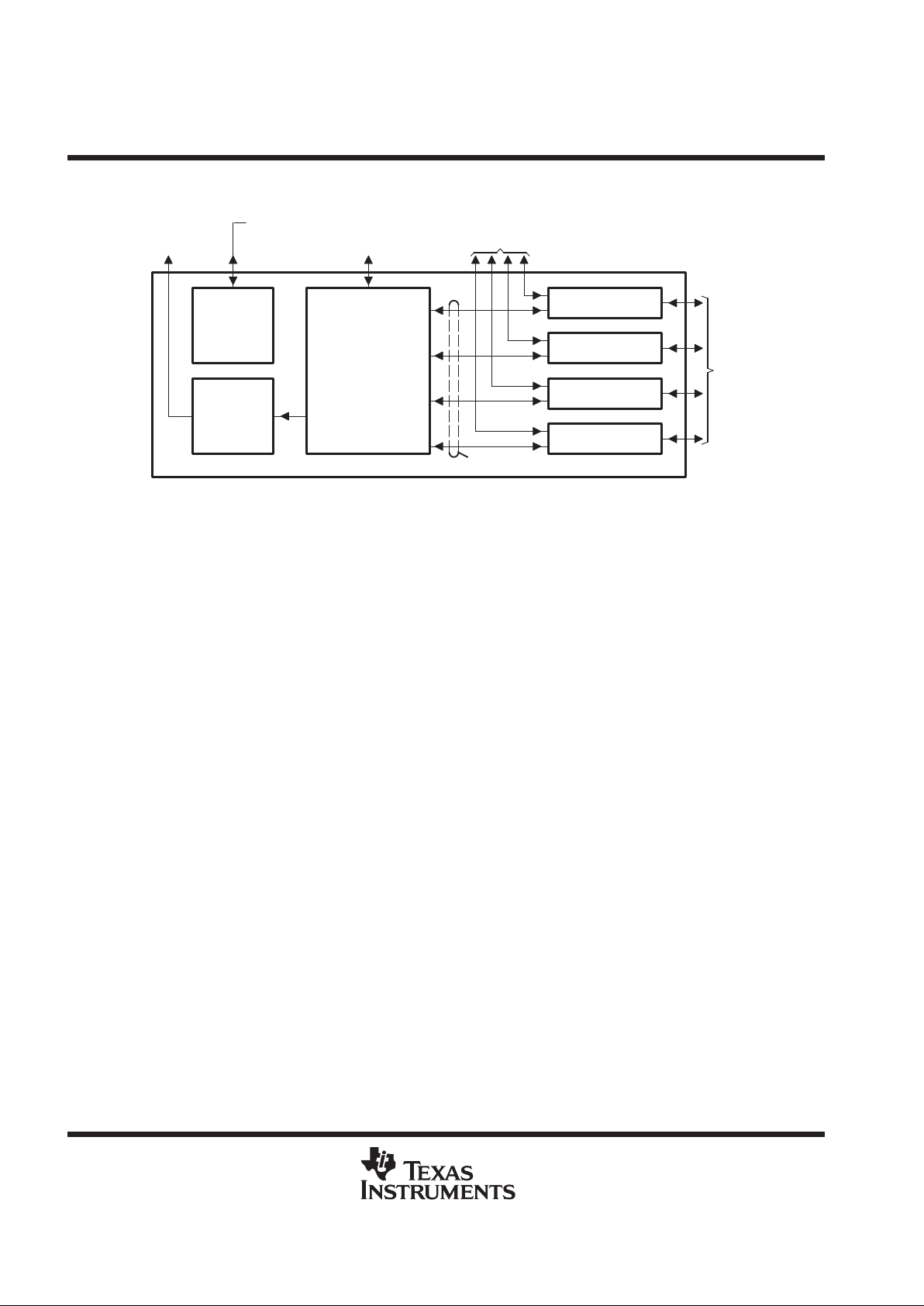
PHY Status and Control Signals
PHY Data I/O
IEEE 1149.1
Std
Test-Access
Port
LED Drivers
MDIO and
TNETE2004 Control
Logic
PHY 3
PHY 2
PHY 1
PHY 0
To/From
10BASE-T
Network
TNETE2004 Control Signals
Manufacturing Test Data
To LED
Status
Indicators
Figure 1. TNETE2004 Architecture
The TNETE2004 provides PHY -interface functions for up to four 10BASE-T half- or full-duplex ports as shown
in Figure 1. The TNETE2004 contains four independent 10BASE-T transceivers in a single chip. Each
transceiver is compliant with IEEE Std 802.3, Section 14, and a compliant management serial-interface port
provides information for network management.
A typical application with external components is shown in Figure 2.
TNETE2004
MDIO-MANAGED QuadPHY
FOUR 10BASE-T PHYSICAL-LAYER INTERFACES
SPWS023D – OCTOBER 1996 – REVISED OCTOBER 1997
3
POST OFFICE BOX 655303 • DALLAS, TEXAS 75265
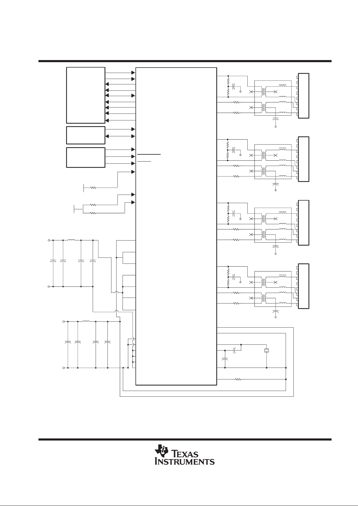
RGND0
FILMAG 23Z128,
23Z356 or equiv.
RJ45C
TGND0
23Z356 or equiv.
FILMAG 23Z128,
RGND1
TGND0
RJ45C
23Z356 or equiv.
FILMAG 23Z128,
RGND2
TGND0
RJ45C
23Z356 or equiv.
FILMAG 23Z128,
RGND3
TGND0
RJ45C
RCVN0
RCVP0
XMTN0
XMTP0
RCVN1
RCVP1
XMTN1
XMTP1
RCVN2
RCVP2
XMTN2
XMTP2
RCVN3
RCVP3
XMTN3
XMTP3
27 pF
20 MHz
TXEN(0–3)
TXD(0–3)
RXCLK(0–3)
DUPLEX(0–3)
LINK(0–3)
CRS(0–3)
COL(0–3)
W–4
W–4
W–4
W–4
W–4
W–4
W–4
W–4
5 V
HF70AC8453215
TNETE2004
10 µF
10 µF
0.1 µF
0.1
µF
27 pF
0.1 µF
0.1 µF
0.1 µF
0.1 µF
MDCLK
MDIO
AUTONEG
LOOPBACK
RESET
SQE
TVDD(0-3)
RVDD(0-3)
LV
DD
LV
DD
LV
DD
TGND(0-3)
RGND(0-3)
LGND
AV
DD
AGND
XTAL1
XTAL2
XGND
IREF
LGND
LGND
LGND
50 Ω
50 Ω
50 Ω
50 Ω
50 Ω
50 Ω
50 Ω
50 Ω
180 Ω
25 Ω
25 Ω
25 Ω
25 Ω
25 Ω
25 Ω
25 Ω
25 Ω
TXCLK
W–4
LV
DD
XV
DD
TNETX3150
System
Controller
V
CC
RXD(0–3)
10 kΩ
TNETX15VEPGE/
TNETX15AEPGE/
TNETX315AL
V
CC
10 kΩ
10 kΩ
CMODE0
CMODE1
5 V
10 µF
10 µF
0.1 µF
GND
AGND
100 pF
100 pF
100 pF
100 pF
Figure 2. External Components for the TNETE2004
TNETE2004
MDIO-MANAGED QuadPHY
FOUR 10BASE-T PHYSICAL-LAYER INTERFACES
SPWS023D – OCTOBER 1996 – REVISED OCTOBER 1997
4
POST OFFICE BOX 655303 • DALLAS, TEXAS 75265
pin assignments
TNETE2004 power supplies are identified according to the section of the device they supply . All power supplies
are labeled VDD or VSS, and each has a single-letter prefix indicating which circuit of the device they supply.
L indicates a supply for control logic, R is for receiver circuits, T is for transmitter circuits, and A is for analog
circuits. Each PHY-specific signal has a suffix, which is the number of the PHY, for example, carrier sense
(CRS0), CRS1, and so on. If a signal name does not include a suffix, it is applicable to all PHYs.
DD
RXCLK0
CRS0
RXD0
LINK0
DUPLEX0
LGND
TGND0
XMTN0
XMTP0
TV
DD0
RV
DD0
RCVN0
RCVP0
RGND0
RESET
LOOPBACK
TGND1
XMTN1
XMTP1
TV
DD1
RV
DD1
RCVN1
RCVP1
RGND1
LGND
DUPLEX1
LINK1
RXD1
CRS1
LV
DD
LV
DD
RXCLK3
CRS3
RXD3
LINK3
DUPLEX3
LGND
RGND3
RCVP3
RCVN3
RV
DD3
TV
DD3
XMTP3
XMTN3
TGND3
SQE
AUTONEG
RGND2
RCVP2
RCVN2
RV
DD2
TV
DD2
XMTP2
XMTN2
TGND2
LGND
DUPLEX2
LINK2
RXD2
CRS2
1
2
3
4
5
6
7
8
9
10
11
12
13
14
15
16
17
18
19
20
21
22
23
24
25
26
27
28
29
93
94
95
96
97
98
99
100
101
102
103
104
105
106
107
108
109
110
111
112
113
114
115
116
117
118
119
120
90
89
88
87
86
85
84
83
82
81
80
79
78
77
76
75
74
73
72
71
70
69
68
67
66
65
64
63
62
59
58
57
56
55
54
53
52
51
50
49
48
47
46
45
44
43
42
41
40
39
38
37
36
35
34
33
32
31
91
92
60
30
61
TXD0
TXEN0
COL0
LED3DUPCOL
LGND
LED3ACTIVE
LED3LINK
LED2DUPCOL
LED2ACTIVE
LED2LINK
LED1ACTIVE
LED1LINK
LED0DUPCOL
LED0ACTIVE
LGND
LED0LINK
TXCLK
MDIO
MDCLK
DEVSEL4
LGND
DEVSEL3
COL3
TXEN3
TXD3
RXCLK1
TXD1
TXEN1
COL1
TCK
TDI
TRST
TMS
IREF
ATEST
CMODE1
XTAL2
PWRDWN
RES1
COL2
TXEN2
TXD2
RXCLK2
LGND
CMODE0
DD
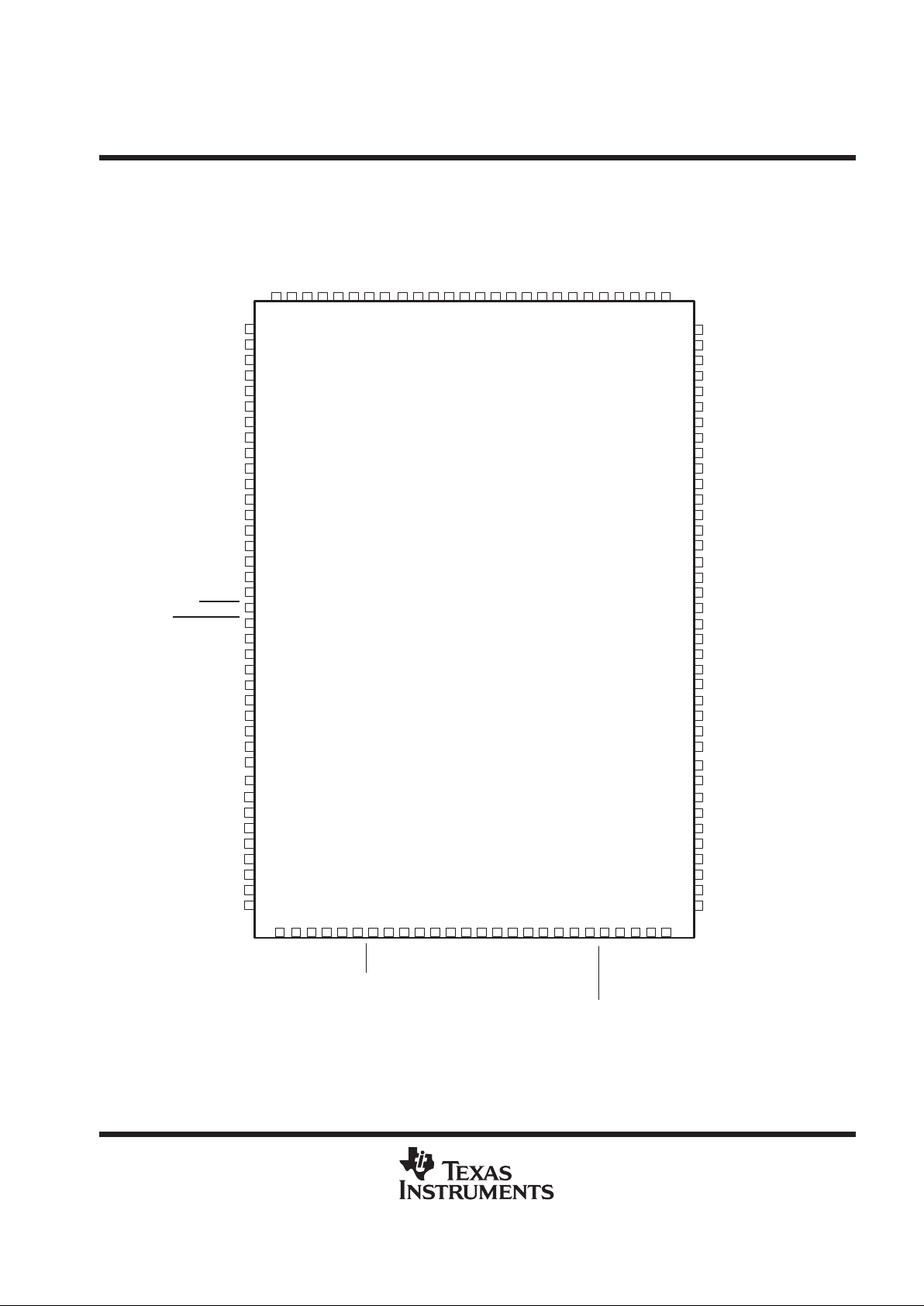
PBE PACKAGE
(TOP VIEW)
LED1DUPCOL
LV
DEVSEL2
TDO
DD
XTAL1
DD
DD
LGND
AGND
LGND
XGND
LV
DD
DD
LV
AV
LV
XV
LV
TNETE2004
MDIO-MANAGED QuadPHY
FOUR 10BASE-T PHYSICAL-LAYER INTERFACES
SPWS023D – OCTOBER 1996 – REVISED OCTOBER 1997
5
POST OFFICE BOX 655303 • DALLAS, TEXAS 75265
DD
TXD0
LV
DD
RXCLK0
CRS0
RXD0
LINK0
DUPLEX0
LGND
TGND0
TGND0
XMTN0
XMTP0
TV
DD0
TV
DD0
RV
DD0
RCVN0
RCVP0
RGND0
RESET
LOOPBACK
TGND1
TGND1
XMTN1
XMTP1
TV
DD1
TV
DD1
RV
DD1
RCVN1
RCVP1
RGND1
LGND
DUPLEX1
LINK1
RXD1
CRS1
LV
DD
RXCLK1
TXEN3
TXD3
LV
DD
RXCLK3
CRS3
RXD3
LINK3
DUPLEX3
LGND
RGND3
RCVP3
RCVN3
RV
DD3
TV
DD3
TV
DD3
XMTP3
XMTN3
TGND3
TGND3
SQE
AUTONEG
RGND2
RCVP2
RCVN2
RV
DD2
TV
DD2
TV
DD2
XMTP2
XMTN2
TGND2
TGND2
LGND
DUPLEX2
LINK2
RXD2
CRS2
LV
DD
1
2
3
4
5
6
7
8
9
10
11
12
13
14
15
16
17
18
19
20
21
22
23
24
25
26
27
28
29
93
94
95
96
97
98
99
100
101
102
103
104
105
106
107
108
109
110
111
112
113
114
115
116
117
118
119
120
90
89
88
87
86
85
84
83
82
81
80
79
78
77
76
75
74
73
72
71
70
69
68
67
66
65
64
63
62
59
58
57
56
55
54
53
52
51
50
49
48
47
46
45
44
43
42
41
40
39
38
37
36
35
34
33
32
31
91
92
60
30
61
COL0
LED3DUPCOL
LGND
LED3ACTIVE
LED3LINK
LED2DUPCOL
LED2ACTIVE
LED2LINK
LED1ACTIVE
LED1LINK
LED0DUPCOL
LED0ACTIVE
LGND
LED0LINK
TXCLK
MDIO
MDCLK
DEVSEL4
LGND
DEVSEL3
COL3
RXCLK2
TXEN1
COL1
LGND
TCK
TDO
TRST
IREF
ATEST
CMODE1
XTAL2
PWRDWN
RES1
COL2
TXEN2
TXD2
LGND
CMODE0
PAC PACKAGE
(TOP VIEW)
LED1DUPCOL
DEVSEL2
TMS
DD
XTAL1
DD
DD
TDI
AGND
LGND
XGND
TXEN0
AV
LV
XV
LV
121
122
123
124
125
126
127
128
TXD1
DD
LV

TNETE2004
MDIO-MANAGED QuadPHY
FOUR 10BASE-T PHYSICAL-LAYER INTERFACES
SPWS023D – OCTOBER 1996 – REVISED OCTOBER 1997
6
POST OFFICE BOX 655303 • DALLAS, TEXAS 75265
Terminal Functions
controller interface
TERMINAL
NO.
I/O
†
DESCRIPTION
NAME
120 128
AUTONEG 74 82 I
Auto-negotiation. When high, AUTONEG enables auto-negotiation on all four PHYs.
Auto-negotiation takes place only after a reset or when a link is reestablished. AUTONEG can be
overridden from the MDI.
COL0
COL1
COL2
COL3
117
34
56
93
127
40
62
103
O
Collision sense. When asserted, COL0–COL3 indicates that PHY0–PHY3 sensed a network
collision. The active level is set by the compatibility pins (see T able 2) or by setting the correct bits
in pin-polarity register 0x16 (see Figure 17). Functions are described in Table 13.
CRS0
CRS1
CRS2
CRS3
2
29
61
88
4
35
67
98
O
Carrier sense. When asserted, CRS0–CRS3 indicates that PHY0–PHY3 is receiving a frame
carrier signal. The active level is set by the compatibility pins (see T able 2) or by setting the correct
bits in pin-polarity register 0x16 (see Figure 17). Functions are described in Table 13.
DUPLEX0
DUPLEX1
DUPLEX2
DUPLEX3
5
26
64
85
7
32
70
95
O/D
Duplex mode. When DUPLEX0–DUPLEX3 is high, PHY0–PHY3 operates in full-duplex mode.
When DUPLEX0–DUPLEX3 is low, PHY0–PHY3 operates in the half-duplex mode. There is an
internal weak drive on DUPLEX0–DUPLEX3 that pulls DUPLEX0–DUPLEX3 if auto-negotiation
chooses the full-duplex mode, or if full duplex is chosen by writing to an MDI register. By connecting
DUPLEX0–DUPLEX3 GND or VDD, this weak drive is overridden, and the type of duplex mode is
permanently set, ignoring any auto-negotiation decisions or values written to the appropriate MDI
registers. To set duplex mode, connect the auto-negotiation pin low. (This turns off
auto-negotiation.)
LINK0
LINK1
LINK2
LINK3
4
27
63
86
6
33
69
96
O
Link status. When LINK0–LINK3 is high, it indicates that PHY0–PHY3 has determined that a valid
10BASE-T link has been established. When low, LINK0–LINK3 indicates that the link has not been
established.
LOOPBACK 16 20 I
Loopback. When low, LOOPBACK enables internal loopback in all four PHYs. When asserted, data
is internally wrapped within each PHY and does not appear on the network. While in the
looped-back state, all network lines are placed in a noncontentious state. LOOPBACK
can be
overridden by the MDI registers.
RXCLK0
RXCLK1
RXCLK2
RXCLK3
1
31
59
89
3
37
65
99
O
Receive clock. Receive clock source for the receive data output RXD0–RXD3. Data is valid on
RXD0–RXD3 on the edges of RXCLK0–RXCLK3 specified by the currently set compatibility mode
(see T able 2) or by setting the correct bits in pin-polarity register 0x16 (see Figure 17). Functions are
described in T able 13.
RXD0
RXD1
RXD2
RXD3
3
28
62
87
5
34
68
97
O Receive data. Bit-wise serial-data output from PHY0–PHY3.
SQE 75 83 I
Signal quality error. When high, SQE causes each PHY to simulate a collision condition at the end
of each frame transmission to test functionality of the collision-detect circuitry. SQE is overridden
by SQEEN (see T able 8). SQE must be set high to interface with the TNETX3150.
TXCLK 101 111 O
Transmit clock. TXCLK is shared by all PHYs to clock in transmit data. Data is valid on TXD0-TDX3
on the edges of TXCLK specified by the currently set compatibility mode (see Table 2) or by
setting the correct bits in pin-polarity register 0x16 (see Figure 17). Functions are described in
Table 13.
TXD0
TXD1
TXD2
TXD3
119
32
58
91
1
38
64
101
I Transmit data. Serial-data input to PHY0–PHY3.
TXEN0
TXEN1
TXEN2
TXEN3
118
33
57
92
128
39
63
102
I
Transmit enable. Assert TXEN0–TXEN3 active to indicate that valid transmit data is on
TXD0–TXD3. The active level is set by the compatibility pins (see T able 2) or by setting the correct
pins in pin-polarity register 0x16 (see Figure 17). Functions are described in Table 13.
†
I = input, O = output, O/D = open-drain output
TNETE2004
MDIO-MANAGED QuadPHY
FOUR 10BASE-T PHYSICAL-LAYER INTERFACES
SPWS023D – OCTOBER 1996 – REVISED OCTOBER 1997
7
POST OFFICE BOX 655303 • DALLAS, TEXAS 75265
Terminal Functions (Continued)
miscellaneous interface
TERMINAL
NO.
TYPE
†
DESCRIPTION
NAME
120 128
ATEST 44 50 A
Analog test pin. ATEST provides access to the filter of the reference PLL. When operating correctly ,
ATEST presents a voltage between 1–2 V.
CMODE0
CMODE1
47
48
53
54
I
Compatibility mode. Eases compatibility with third-party media-access controllers (MACs) (see
Table 2).
DEVSEL2
DEVSEL3
DEVSEL4
95
96
98
105
106
108
I
Device select. DEVSEL2–DEVSEL4 specifies the three most-significant bits of a 5-bit number used
to address a PHY on the management-data interface. The two least-significant bits are set as 00,
01, 10, and 11 for PHY0–PHY3, respectively.
IREF 43 49 A
Current reference. Used to set a current reference for the analog circuitry. IREF must be connected
to ground by a 180 ± 5-Ω resistor.
MDCLK 99 109 I Management-data clock. MDCLK is used to clock data in and out of the MDIO port.
MDIO 100 110 I/O Management-data I/O. MDIO is the serial management-data interface.
PWRDWN 54 60 I
Power down. When asserted, PWRDWN places all four PHYs in the lower power state.
Transmitting and receiving are inhibited in this state.
RES1 55 61 O Reserved
RESET 15 19 I Global reset. RESET is used to reset all four PHY sections.
XTAL1 50 56 A
Crystal oscillator pins. Connect a 20-MHz crystal across XTAL1 and GND, or drive XTAL1 from a
20-MHz crystal-oscillator module.
XTAL2 51 57 A
Connect a 27-pF capacitor across XTAL2 and XT AL1 and connect a 27-pF capacitor between XT AL2
and GND. If a crystal-oscillator module is used, do not connect anything to XTAL2.
†
A = analog, I = input, O = output, I/O = 3-state input/output
JTAG interface
TERMINAL
NO.
I/O
‡
DESCRIPTION
NAME
120 128
TCK 36 42 I
Test clock. TCK is used to clock state information and test data into and out of the device during
operation of the JTAG.
TDI 37 43 I
Test data input. TDI is used to serially shift test data and test instructions into the device during
operation of the JTAG.
TDO 38 44 O
T est data output. TDO is used to serially shift test data and test instructions out of the device during
operation of the JTAG.
TMS 40 46 I Test mode select. TMS controls the operating state of the JTAG.
TRST 39 45 I Test reset. TRST is used for asynchronous reset of the JT AG controller.
‡
I = input, O = output

TNETE2004
MDIO-MANAGED QuadPHY
FOUR 10BASE-T PHYSICAL-LAYER INTERFACES
SPWS023D – OCTOBER 1996 – REVISED OCTOBER 1997
8
POST OFFICE BOX 655303 • DALLAS, TEXAS 75265
Terminal Functions (Continued)
LED interface
TERMINAL
NO.
I/O
†
DESCRIPTION
NAME
120 128
LED0ACTIVE
LED1ACTIVE
LED2ACTIVE
LED3ACTIVE
105
108
111
114
115
118
121
124
O
LED activity indicator. The LED activity indicator is driven low for 20 ms when PHY0–PHY3
receives or transmits. LED0ACTIVE–LED3ACTIVE can sink a 10-mA current. If it receives or
transmits another packet during that 20 ms, the LED does not flash, but stays on. Therefore,
if packets are received or transmitted at intervals faster than 20 ms, the LED stays on
continuously.
LED0DUPCOL
LED1DUPCOL
LED2DUPCOL
LED3DUPCOL
106
109
112
116
116
119
122
126
O
LED duplex/collision indicator for PHY0–PHY3. This LED status pin has different meaning when
in full- or half-duplex mode. In full-duplex mode, LED0DUPCOL–LED3DUPCOL is continuously
driven low. In half-duplex mode, it is driven low for 20 ms after a collision.
LED0DUPCOL–LED3DUPCOL can sink a 10-mA current.
LED0LINK
LED1LINK
LED2LINK
LED3LINK
103
107
110
113
113
117
120
123
O
LED link indicator. The LED link indicator is driven low when PHY0–PHY3 has established a
valid link. LED0LINK–LED3LINK can sink a 10-mA current.
†
O = output
10BASE-T interface
TERMINAL
NO.
TYPE
‡
DESCRIPTION
NAME
120 128
XMTN0
XMTN1
XMTN2
XMTN3
8
18
67
77
11
23
74
86
p
p
XMTP0
XMTP1
XMTP2
XMTP3
9
19
68
78
12
24
75
87
A
Transmit pair. Differential line-transmitter outputs from PHY0–PHY3
.
RCVN0
RCVN1
RCVN2
RCVN3
12
22
71
81
16
28
79
91
Receive pair for PHY0–PHY3. Differential line-receiver inputs connect to receive pair through
RCVP0
RCVP1
RCVP2
RCVP3
13
23
72
82
17
29
80
92
A
g
transformer isolation.
‡
A = analog

TNETE2004
MDIO-MANAGED QuadPHY
FOUR 10BASE-T PHYSICAL-LAYER INTERFACES
SPWS023D – OCTOBER 1996 – REVISED OCTOBER 1997
9
POST OFFICE BOX 655303 • DALLAS, TEXAS 75265
Terminal Functions (Continued)
power interface
TERMINAL
NO.
TYPE
†
DESCRIPTION
NAME
120 128
AGND 45 51 GND Ground pin for analog circuitry
AV
DD
42 48 PWR VDD pin for analog circuitry
6, 25 8, 31
6, 25
35, 46
8, 31
41, 52
LGND
,
65, 84,71, 94
GND
Logic ground pin
,
94, 97,104, 107
gg
104, 115 114, 125
LV
DD
30, 41
53, 60
90, 102
120
36, 47
59, 66
100, 112
2
PWR Logic VDD pin
RGND0
RGND1
142418
30
p
RGND2 73 81
GND
Ground pin for receiver circuitr
y
RGND3 83 93
RV
DD0
RV
DD1
RV
DD2
RV
DD3
11
21
70
80
15
27
78
90
PWR VDD pin for receiver circuitry
TGND0
TGND1
7
17
9, 10
21, 22
p
TGND2
TGND3
66
76
,
72, 73
84, 85
GND
Ground pin for transmit circuitr
y
TV
DD0
TV
102013, 14
25, 26
p
DD1
TV
DD2
69
,
76, 77
PWR
V
DD
pin for transmit circuitr
y
DD2
TV
DD3
79 88, 89
XGND 49 55 GND Ground pin for crystal-oscillator circuitry
XV
DD
52 58 PWR VDD pin for crystal-oscillator circuitry
†
GND = ground, PWR = power
TNETE2004
MDIO-MANAGED QuadPHY
FOUR 10BASE-T PHYSICAL-LAYER INTERFACES
SPWS023D – OCTOBER 1996 – REVISED OCTOBER 1997
10
POST OFFICE BOX 655303 • DALLAS, TEXAS 75265
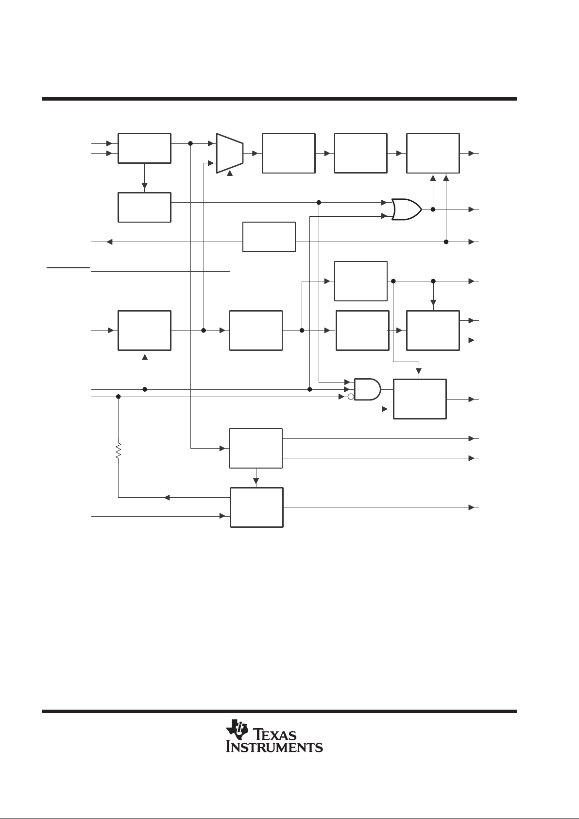
functional block diagram
Receiver
RCVP
RCVN
1
0
Digital
PLL
Decoder
Manchester
RXD
Clock
Generator
Watchdog
Timer
Line
Driver
D-to-A
Converter
Manchester
Encoder
Generator
Collision
CRS
RXCLK
JABBER
XMTP
XMTN
COL
TXCLK
TXEN
DUPLEX
SQE
AUTONEG
LINK
Remote
Fault
TXD
Carrier Sense
Smart
Squelch
Elastic
Buffer
Disable
Link
Fail
LOOPBACK
Link-Pulse
Detector
Auto-
Negotiation
Wave-
Shaping
Filter

TNETE2004
MDIO-MANAGED QuadPHY
FOUR 10BASE-T PHYSICAL-LAYER INTERFACES
SPWS023D – OCTOBER 1996 – REVISED OCTOBER 1997
11
POST OFFICE BOX 655303 • DALLAS, TEXAS 75265
functional description
The TNETE2004 consists of four PHYs, with each PHY having several logical blocks (see the functional block
diagram and Table 1).
Table 1. Logical Blocks
LOGICAL BLOCKS FUNCTION
Transmitter function Accepts data from the data terminal equipment (DTE) and transmits it onto the network
Receiver function Receives data from the network and sends it to the DTE
Collision/signal-quality error detection Indicates to the DTE any collision on the network/transmitter with valid link
Jabber detection Indicates to the DTE if a packet transmission exceeds 20-ms minimum
Auto-negotiation Negotiate to establish the highest common protocol
Management-data interface To allow register-based management operations for each PHY module
Link test A link pulse is sent to indicate a valid connection.
LED status indicator Indication for link, activity, and collision
Test port IEEE Std 1149.1 test-access port and boundary-scan testing
Loopback test mode
Loopback capabilities are provided to allow certain tests to be performed to validate operation of
the TNETE2004.
Compatibility modes Ease connection to third-party MACs
10BASE-T differential line-transmitter function
Each differential line driver of the TNETE2004 drives a balanced, properly terminated twisted-pair transmission
line with a characteristic impedance of 85 Ω to 111 Ω (see Figure 2). In the idle state, the driver maintains a
minimum differential output voltage, while staying within the required common-mode voltage range.
The driver incorporates an on-chip wave-shaping stage and a high-frequency filtering stage to allow the outputs
to be connected directly to isolation transformers through serial termination resistors. No external filters are
required.
Serial data for transmission by a PHY is presented to the appropriate transmit data (TXD) input of the
TNETE2004. To be valid, data must be synchronized on the appropriate edges of the transmit clock (TXCLK)
signal, which depends on the compatibility-mode setting.
Once the transmit-enable (TXEN) pin is deasserted for a PHY, the driver maintains full differential outputs for
a minimum of 250 ns, which then begins to decay to minimum differential levels.
The PHY also transmits regular link pulses in compliance with IEEE Std 802.3.
10BASE-T differential line-receiver function
The line-receiver pins of each PHY must be connected to a properly terminated transmission line by an external
isolation transformer. The receiver establishes its own common-mode input-bias voltage. Data received from
the network is output on RXD of the appropriate PHY and synchronized by the appropriate edges of the
corresponding RXCLK signal, which depends on the compatibility-mode setting.
The receiver incorporates a squelch function to pass incoming data. This smart squelch function passes data
only if the input amplitude is greater than a minimum signal threshold and if a specific pulse sequence is
received. This protects input data from impulse line noise being mistaken for signal or link activity . The squelch
circuits quickly deactivate if received pulses exceed the specifications; thus, overly long pulses are not mistaken
as link pulses.
Carrier sense (CRS) is driven high while the squelch function is active to indicate that the circuit is allowing data
to pass from the twisted pair. CRS is driven low when the squelch circuit is disabling data low.

TNETE2004
MDIO-MANAGED QuadPHY
FOUR 10BASE-T PHYSICAL-LAYER INTERFACES
SPWS023D – OCTOBER 1996 – REVISED OCTOBER 1997
12
POST OFFICE BOX 655303 • DALLAS, TEXAS 75265
collision/signal-quality error detection
When not in full-duplex mode, collisions are detected by sensing simultaneous activity on both the transmit and
the receive pins. A collision detection is signified by COL on the respective PHY being driven high for the
duration of the condition and for a specified time afterwards.
The TNETE2004 device also provides a signal-quality error (SQE) function. This function can be enabled or
disabled only for the whole device and not for individual PHYs. When SQE is enabled, following transmission,
a simulated collision is presented to a PHY. PHY tests as much of the collision-detect circuitry as possible
without affecting the attached twisted-pair channels. Each PHY asserts its COL output signal high for a defined
time interval relative to the last positive data edge of its transmit data input. SQE is invoked by driving SQE high
or by using the TNETE2004 registers.
jabber detection
Each PHY monitors the length of the packet being transmitted. If a single packet exceeds 20 ms, a jabber
condition is detected. The output is disabled, and CRS is driven low. The TNETE2004 device asserts COL, while
attempts are made to transmit data, and signals link-fail for the duration of the attempts. The device also asserts
COL (for half-duplex mode only) when it has detected that the transmitter has entered jabber mode. To clear
the jabber function, transmission must cease for a minimum of 500 ms.
auto-negotiation
Each PHY on the device is capable of auto-negotiation as defined in IEEE Std 802.3. When enabled, this feature
allows a PHY to negotiate with another PHY on the link to establish their highest common protocol. Until a PHY
has completed its negotiation, it cannot assert LINK.
The only two protocols possible for the TNETE2004 are half- or full-duplex 10BASE-T. When auto-negotiation
indicates that full-duplex operation is possible, a weak pullup resistor is applied to DUPLEX on the device,
allowing full-duplex operation, unless the pin is pulled low externally.
link-partner register
This register contains the information for the link partner. Refer to Table 6 for the link partner’s ability-register
bit functions.
expansion register
Refer to Table 7 for the bit definition on the expansion register.
next_page transmit
After exchanging the base page, which contains the information to make connection automatically , if both ends
of the link indicate support for the next_page function, additional data can be exchanged. This allows extensions
to the standard and proprietary extensions to exist without affecting interoperability . Refer to Figure 11 for the
next_page transmit register.
management-data interface
The TNETE2004 incorporates a management-data interface to allow register-based management operations
for each PHY module. Operation of the TNETE2004 is possible without use of the management-data interface,
since all the signals necessary for complete functionality are accessible by way of the device pins; however,
some additional features are accessible only through the management-data interface.
interrupt enable cycle
The TNETE2004 can generate interrupts via the MDIO interface after the quiescent cycle. The quiescent cycle
is the cycle following the data transfer in which neither the external MAC nor the PHYs drive MDIO. The
TNETE2004 indicates to the host that an interrupt is pending by driving MDIO low. This happens one clock cycle
after the quiescent cycle, while MDCLK is high. When MDCLK goes low, TNETE2004 stops driving MDIO so
the host can determine what caused the interrupt.

TNETE2004
MDIO-MANAGED QuadPHY
FOUR 10BASE-T PHYSICAL-LAYER INTERFACES
SPWS023D – OCTOBER 1996 – REVISED OCTOBER 1997
13
POST OFFICE BOX 655303 • DALLAS, TEXAS 75265
link test
When not in auto-negotiation mode, the PHY sends link pulses, separated by an interval of 16 ms, on the
data-out (DO) circuit. The receiver looks for valid link pulses on the input pair. If a link pulse is not received within
a given time interval, the device enters a link-fail state. In this state, link pulses continue to be generated, and
the receiver constantly looks for the link-pulse pattern. The device remains in this state until a valid receive
packet or multiple legal link-test pulses are received.
loopback test mode
By asserting the LOOPBACK pin on the device or by setting the LOOPBACK bit in the PHY generic control
register, the transmit circuit of each PHY is looped to the corresponding receive circuit closest to the twisted-pair
I/O pins. Thereafter, transmit drivers do not forward any further packet data but continue to send link-test pulses.
When accessing loopback test mode from the package pins, since there is only one LOOPBACK pin on the
package, all four PHYs are placed in LOOPBACK mode simultaneously. Individual PHYs can be placed in
LOOPBACK mode by means of the TNETE2004 registers. While in LOOPBACK mode, all receive activities,
other than link-test pulses, are ignored. However, squelch information is still processed, allowing the link status
to be maintained under momentary loopback self-test.
LED status indication
The TNETE2004 has 12 pins that drive LEDs. Each PHY has the following three status LEDs:
Note: The LEDs are all off when reset is active. Once reset is inactive, all the LEDs turn on for 100ms, then turn
off, and then function in the normal way. The following signals are active low.
LEDxLINK – illuminates when PHYx has established a valid link
LEDxACTIVE – illuminates when PHYx is transmitting or receiving data. This LED illuminates for a minimum
duration of 20 ms for each activity , but if packets are being received or transmitted faster than
20 ms, it stays on continuously.
LEDxDUPCOL – illuminates continuously when PHYx is in full-duplex mode. Illuminates for a minimum
duration of 20 ms when collisions occur in half-duplex mode. Additionally, in half-duplex
mode, LED0DUPCOL–LED3DUPCOL flashes when a jabber condition is detected. This
feature is not available in full-duplex mode.
IEEE Std 1149.1 (JTAG) test port
Compliant with the IEEE Std 1 149.1, the test-access port is composed of five pins. These pins interface serially
with the device and the board on which the device is installed for boundary-scan testing. The TNETE2004
implements the following JTAG instructions:
000 EXTEST External boundary-scan test
001 SAMPLE/PRELOAD Initialization for boundary-scan test
100 IDCODE Scans out TNETE2004 identification code
101 HIGHZ Sets all digital output pins on the TNETE2004 to high impedance
111 BYPASS Connects 1-bit bypass register between TDI and TDO

TNETE2004
MDIO-MANAGED QuadPHY
FOUR 10BASE-T PHYSICAL-LAYER INTERFACES
SPWS023D – OCTOBER 1996 – REVISED OCTOBER 1997
14
POST OFFICE BOX 655303 • DALLAS, TEXAS 75265
autopolarity
The TNETE2004 can sense and detect reversed polarity of its receiver inputs (e.g., due to incorrect cable
wiring). If, at any time, seven consecutive inverted link pulses are detected, then reversed polarity is assumed
and flagged by the POLOK bit in the TNETE2004_sts register (see Table 9). If automatic polarity correction is
selected by the SWAPPOLEN bit in the TNETE2004_ctl register (see T able 8), the TNETE2004 swaps its RCVP
and RCVN input for the affected PHY. Once a single correct link pulse is received, good polarity is assumed,
and the POLOK bit is set.
Automatic polarity correction is enabled by default after power on or reset. The polarity detect circuit must see
link pulses to detect the polarity of the receive pair, so, in instances of high network activity where link pulses
are sparse, there may be a slight delay before the correct polarity is established.
compatibility modes
T o ease connection to third-party MACs, the TNETE2004 provides options to reverse the polarity of some device
pins. The compatibility mode is selected by the CMODE0 and CMODE1 pins, as defined in Table 2. The
TNETE2004 can be programmed through the MDIO to change the polarity of each SNI (like COL or RXCLK,
etc.) signal. Refer to Table 13 for more details on this function.
Table 2. Compatibility Mode Options
CMODE PIN SIGNIFICANCE
Mode 1:
CMODE0 = Low
CMODE1 = Low
CRS high to indicate carrier detected
COL high to indicate collision
TXEN high to indicate valid data on TXD
Data on RXD valid on rising edge of RXCLK
Data on TXD valid on rising edge of TXCLK
RXD high when no data is being received
RXCLK is continuously running.
Mode 2:
CMODE0 = High
CMODE1 = Low
CRS low to indicate carrier detected
COL low to indicate collision
TXEN low to indicate valid data on TXD
Data on RXD valid on falling edge of RXCLK
Data on TXD valid on falling edge of TXCLK
RXD high when no data is being received
RXCLK runs for seven clocks after CRS is high,
then it stays high.
Mode 3:
CMODE0 = Low
CMODE1 = High
CRS high to indicate carrier detected
COL low to indicate collision
TXEN high to indicate valid data on TXD
Data on RXD valid on falling edge of RXCLK
Data on TXD valid on falling edge of TXCLK
RXD low when no data is being received
RXCLK runs for seven clocks after CRS is low,
then it stays high.
Mode 4:
CMODE0 = High
CMODE1 = High
CRS high to indicate carrier detected
COL high to indicate collision
TXEN high to indicate valid data on TXD
Data on RXD valid on rising edge of RXCLK
Data on TXD valid on rising edge of TXCLK
RXD low when no data is being received
RXCLK is continuously running.

TNETE2004
MDIO-MANAGED QuadPHY
FOUR 10BASE-T PHYSICAL-LAYER INTERFACES
SPWS023D – OCTOBER 1996 – REVISED OCTOBER 1997
15
POST OFFICE BOX 655303 • DALLAS, TEXAS 75265
TNETE2004 registers
The TNETE2004 incorporates management-data interface to allow register-based management operations for
each PHY module. Normal operation of the TNETE2004 is possible without use of management-data interface
since all the essential signals for operation are accessible through the device pins; however, some additional
features are accessible only through the management-data interface. If management-data interface is not being
used, DEVSEL, MDCLK, and MDIO all can be tied low.
Some features are controllable by both pins and registers. A feature is controlled by the pin until a write operation
is performed on the register controlling the feature. From then until the device is reset, the value on the pin is
ignored.
The TNETE2004 registers are accessible through the Mll-management interface. The IEEE Std 802.3 Mll serial
protocol allows for up to 32 different PHYs, with up to 32 (16-bit-wide) internal registers in each device.
The TNETE2004 implements 11 registers (three of which are hardwired) on each PHY and three additional
overview registers that allow software drivers to access all four PHYs in a single operation. User programming
of the SNI is implemented through the pin-polarity register. These all-PHY registers are mapped into the
addressing space on PHY0.
Figure 3 shows the TNETE2004 device register map. The registers, shown shaded, are the generic registers
mandated by the Mll specification. The unshaded registers are TI-specific registers.
PHY Generic Control Register (see Figure 6, Table 3)
GEN_sts
QuadPHY_sts
QuadPHY_4ctl
QuadPHY_4sts
QuadPHY_4ctl2
QuadPHY_ppol
0x00
0x01
0x02
0x03
0x04
0x05
0x06
0x07
0x08 to 0x0f
0x10
0x11
0x12
0x13
0x14
0x15
0x16
Address
PHY Generic Status Register (see Figure 7, Table 4)
PHY Generic Identifier (high), hardwired 0x4000
PHY Generic Identifier (low), hardwired 0x5051
Auto-Negotiation Advertisement (see Figure 8, Table 5)
Auto-Negotiation Link-Partner Ability (see Figure 9, Table 6)
Auto-Negotiation Expansion (see Figure 10, Table 7)
Auto-Negotiation Next-Page Transmit (see Figure 11)
Reserved by IEEE Std 802.3
TNETE2004 Identification, Hardwired
TNETE2004 Control Register (see Figure 12, Table 8)
TNETE2004 Status Register (see Figure 13, Table 9)
TNETE2004 Nibble-Based Control Register, Overview (see Figure 14, Table 10)
TNETE2004 Nibble-Based Status Register , Overview (see Figure 15, Table 11)
TNETE2004 Nibble-Based Control Register 2, Overview (see Figure 16, T able 12)
TNETE2004 Pin-Polarity Register (see Figure 17, T able 13)
Register
AN_NEXTPAGE
Reserved
GEN_id_hi
GEN_id_lo
AN_far_end_ability
AN_exp
AN_advertisement
GEN_ctl
QuadPHY_ID
QuadPHY_ctl
GEN_sts
Figure 3. TNETE2004 Registers
The default or IDLE state of the two-wire Mll is a logic 1. All 3-state drivers are disabled, and the TNETE2004
pullup resistor pulls the MDIO line to a logic 1. Before initiating any other transaction, the station management
entity sends a sequence of 32 contiguous logic 1 bits on MDIO and 32 corresponding contiguous logic 1 bits
on MDCLK. This sequence provides the TNETE2004 with a pattern that it can use to establish synchronization.
The TNETE2004 responds to no other transactions until it recognizes a sequence of 32 contiguous logic 1 bits
on MDIO with 32 contiguous logic 1 bits on MDCLK.
Frame format of the generic registers is in accordance with Mll specifications as shown in Figures 4 and 5.

TNETE2004
MDIO-MANAGED QuadPHY
FOUR 10BASE-T PHYSICAL-LAYER INTERFACES
SPWS023D – OCTOBER 1996 – REVISED OCTOBER 1997
16
POST OFFICE BOX 655303 • DALLAS, TEXAS 75265
Start Delimiter Operation Code PHY Address Register Address Turnaround Data
01
10 AAAAA RRRRR Z0 DDDD.DDDD.DDDD.DDDD
Figure 4. MII Frame Format: Reads
Start Delimiter Operation Code PHY Address Register Address Turnaround Data
01
01 AAAAA RRRRR 10 DDDD.DDDD.DDDD.DDDD
Figure 5. MII Frame Format: Writes
start delimiter
The start of a frame is indicated by a 01 pattern. This pattern ensures transitions from the default logic 1 line
state to 0 and back to 1.
operation code
The operation code for a read is 10, while the code for a write is 01.
PHY address
The PHY address is five bits wide, which allows 32 unique PHY addresses. The first PHY address bit transmitted
and received is the most-significant bit (MSB) of the address. The two least-significant bits (LSBs) represent
the PHY number within the package. The upper three bits for each internal PHY are read from the DEVSEL pins.
register address
The register address is five bits wide, allowing 32 individual registers to be addressed within each PHY. Refer
to the address maps (Figures 4 and 5) for the addresses of individual registers.
turn around
An idle-bit time, during which no device actively drives the MDIO signal, must be inserted between the register
address field and the data field of a read frame, to avoid contention. During a read frame, the PHY drives a
0 bit onto MDIO for the bit time following the idle bit and preceding the data field. During a write frame, this field
must consist of a 1 bit followed by a 0 bit.
data
The data field is composed of 16 bits. The first data bit transmitted and received is the MSB of the data payload.

TNETE2004
MDIO-MANAGED QuadPHY
FOUR 10BASE-T PHYSICAL-LAYER INTERFACES
SPWS023D – OCTOBER 1996 – REVISED OCTOBER 1997
17
POST OFFICE BOX 655303 • DALLAS, TEXAS 75265
PHY generic control register – GEN_ctl at 0x0
BYTE 1
15
14 13 12 11 10 9 8 7 6 5 4 3 2 1
BYTE 0
0
R
E
S
E
T
L
O
O
P
B
A
C
K
0 A
N
E
N
A
B
L
E
P
D
O
W
N
I
S
O
L
A
T
E
A
N
R
E
S
T
A
R
T
D
U
P
L
E
X
C
O
L
T
E
S
T
RESERVED
Figure 6. PHY Generic Control Register
Table 3. PHY Generic Control Register Bit Functions
BIT
NO.
NAME
FUNCTION
DIRECTION
†
DEFAULT
15 RESET
‡
Reset a PHY. Writing a 1 RESET resets the whole device, and all registers revert to
their default values. RESET is self clearing. It is always read as 0. It is not possible
to reset one PHY separately from the others. Operation of the device is not ensured
for a duration of 50 ms after a software reset.
R/W 0
14 LOOPBACK
Internal loopback mode. LOOPBACK enables the internal loopback within the
individual PHY. When LOOPBACK is set to 1, data is wrapped internally within the
PHY and does not appear on the network. Collision detection is disabled, and data
transmitted appears at the receive pins. While in loopback mode, the device pins are
placed in noncontentious states.
R/W Pin
13 Reserved RO 0
12 ANENABLE
Auto-negotiation enable. When set, ANENABLE allows auto-negotiation to take
place.
R/W Pin
11 PDOWN
Power-down mode. When set, PDOWN places the PHY in a power-down mode. In
this mode, it is not possible to receive or transmit data, although it is possible to
continue to process management-data frames. IEEE Std 802.3 states that the PHY
must be allowed 500 ms of initialization time after it is taken out of power-down state
before data transmission and reception can be started. See Note 1.
R/W 0
10 ISOLATE
PHY pin isolation. When set, the PHY electrically isolates itself from the pins. In the
ISOLATE state, the PHY does not respond to TXD or TXEN but presents a high
impedance on RXD, RXCLK, and COL. However, it still responds to MII data frames.
R/W 0
9 ANRESTART Auto-negotiation restart. Setting ANRST causes auto-negotiation to be restarted. R/W 0
8 DUPLEX
Full-duplex mode select. Setting DUPLEX forces this PHY into full-duplex mode.
Resetting it forces half-duplex. For DUPLEX to have any effect, the DUPLEX pin on
the package must not be driven externally.
R/W Pin
7 COLTEST
Collision-test enable. Setting COL TEST causes this PHY to assert COL when TXEN
is asserted.
R/W 0
6–0 RESERVED Reserved 0
†
RO = read only, R/W = read/write
‡
This bit is set for the TNETE2004, not for each PHY.
NOTE 1: If all four PHYs are in power-down mode simultaneously, then reset must be used to power up the device. It is not possible to power
up an individual PHY if all four PHYs are in power-down mode.

TNETE2004
MDIO-MANAGED QuadPHY
FOUR 10BASE-T PHYSICAL-LAYER INTERFACES
SPWS023D – OCTOBER 1996 – REVISED OCTOBER 1997
18
POST OFFICE BOX 655303 • DALLAS, TEXAS 75265
PHY generic status register – GEN_sts at 0x1
BYTE 1
15
14 13 12 11 10 9 8 7 6 5 4 3 2 1
BYTE 0
0
0
0 0 1 1
RESERVED
A
C
O
M
P
L
E
T
E
R
F
A
U
L
T
1 L
I
N
K
J
A
B
B
E
R
1
Figure 7. PHY Generic Status Register
Table 4. PHY Generic Status Register Bit Functions
BIT
NO.
NAME
FUNCTION
DIRECTION
†
15 100Base-T4 capable. Not supported, read as 0 RO
14 100Base-T4 full-duplex capable. Not supported, read as 0 RO
13 100Base-T4 half-duplex capable. Not supported, read as 0 RO
12 10BASE-TX full-duplex capable. Supported, read as 1 RO
11 10BASE-TX half-duplex capable. Supported, read as 1 RO
10–6 RESERVED Reserved. Read as 0. RO
5 ACOMPLETE
Auto-negotiation complete. When set, ACOMPLETE indicates that auto-negotiation has been
completed.
RO
4 RFAULT
Remote fault detected. When set, RFAULT indicates that the link partner has indicated a fault
condition by way of auto-negotiation.
RO
3 Auto-negotiation capable. Set to indicate this PHY is capable of auto-negotiation RO
2 LINK Link status. When set, LINK indicates that the PHY is receiving valid link pulses. RO
1 JABBER
Jabber detected. When set, JABBER indicates the PHY has entered jabber mode. JABBER is
cleared after a reset or after TXEN is deasserted for 500 ms.
RO
0
Extended capability . This bit is hardwired to 1 to indicate that the PHY supports extensions to the
IEEE Std 802.3u.
RO
†
RO = read only
PHY generic identifier, GEN_id_hi, and GEN_id_lo at 0x2 and 0x3
These two registers are hardwired to constant values. GEN_id_hi is fixed at 0x4000, and GEN_id_lo is fixed
at 0x5051.

TNETE2004
MDIO-MANAGED QuadPHY
FOUR 10BASE-T PHYSICAL-LAYER INTERFACES
SPWS023D – OCTOBER 1996 – REVISED OCTOBER 1997
19
POST OFFICE BOX 655303 • DALLAS, TEXAS 75265
auto-negotiation advertisement register at 0x4
BYTE 1
15
14 13 12 11 10 9 8 7 6 5 4 3 2 1
BYTE 0
0
N
X
T
P
A
G
E
R
E
S
E
R
V
E
D
R
F
L
T
TECHNOLOGY ABILITY FIELD SELECTOR FIELD
Figure 8. Auto-Negotiation Advertisement Register
Table 5. Auto-Negotiation Advertisement-Register Bit Functions
BIT
NO.
NAME
FUNCTION
DIRECTION
†
DEFAULT
15 NXTPAGE
Auto-negotiation next page. NXTPAGE should be set when there is a next
page to transmit. The next page is set by writing to AN_NEXTPAGE.
RO 0
14 RESERVED Reserved RO 0
13 RFLT
Remote fault. RFLT enabled indicates to the link partner that there is a fault
condition on the TNETE2004. RFL T can be set only by a management entity .
This bit does not imply an internal test mode.
R/W 0
12–5
TECHNOLOGY
ABILITY FIELD
‡
This field indicates the technology abilities advertised to the link partner.
Unsupported technologies cannot be transmitted, hence, only two bits have
significance.
Bit 6: Full-duplex 10BASE-T
Bit 5: Half-duplex 10BASE-T
All other bits are hardwired to 0.
R/W
Bits 5 and 6
are set to 1, all
others are set
to 0.
4–0
SELECTOR
FIELD
This field specifies the format of the page to be transmitted. This PHY supports
only standard IEEE Std 802.3u base pages, so this field is hardwired to 00001.
RO
†
RO = read only, R/W = read/write
‡
After a reset, the PHY attempts to drive the duplex pin. If the pin can be driven high, then bit 6 is set. If the pin can be driven low, then bit 5 is
set.
auto-negotiation link-partner ability register at 0x5
This register contains the most recently received link control word from the remote PHY. Writing to this register
has no effect. The contents of this register are undefined unless either ACOMPLETE (bit 5, register 1) or
PAGERX (bit 1, register 6) are set.
When ACOMPLETE is set, the bits in this register are as described in Table 6.
BYTE 1
15
14 13 12 11 10 9 8 7 6 5 4 3 2 1
BYTE 0
0
L
P
N
X
T
P
A
G
E
R
E
S
E
R
V
E
D
L
P
R
F
L
T
LINK-PARTNER
TECHNOLOGY ABILITY FIELD
LINK-PARTNER
SELECTOR FIELD
Figure 9. Auto-Negotiation Link-Partner Ability Register
TNETE2004
MDIO-MANAGED QuadPHY
FOUR 10BASE-T PHYSICAL-LAYER INTERFACES
SPWS023D – OCTOBER 1996 – REVISED OCTOBER 1997
20
POST OFFICE BOX 655303 • DALLAS, TEXAS 75265
auto-negotiation link-partner ability register at 0x5 (continued)
Table 6. Auto-Negotiation Link-Partner Ability Register Bit Functions
BIT
NO.
NAME
FUNCTION
DIRECTION
†
15 LPNXTPAGE
Link-partner auto-negotiation next page. LPNXTPAGE indicates that the link partner has
another page to send.
RO
14 RESERVED Reserved RO
13 LPRFLT Link-partner remote fault. LPRRFLT indicates that the link partner is reporting a fault condition. RO
12 RESERVED Reserved for future abilities. Read as 0. RO
11 RESERVED Reserved for future abilities. Read as 0. RO
10 RESERVED Reserved for future abilities. Read as 0. RO
9 100BASE-T4 100Base-T4 is supported by the link partner. RO
8 100BASE-TXFD 100Base-TX full-duplex is supported by the link partner. RO
7 100BASE-TXHD 100Base-TX half-duplex is supported by the link partner . RO
6 10BASE-TFD 10BASE-T full-duplex is supported by the link partner. RO
5 10BASE-THD 10BASE-T half-duplex is supported by the link partner. RO
4–0
LINK-PAR TNER
SELECTOR
FIELD
Identifies the format of this register. The IEEE Std 802.3u base page is indicated by code
00001.
RO
†
RO = read only
When P AGERX is set, this register contains a direct copy of the next page received. PAGERX is cleared on a
read from this register.
auto-negotiation expansion register – AN_exp at 0x6
BYTE 1
15
14 13 12 11 10 9 8 7 6 5 4 3 2 1
BYTE 0
0
RESERVED
P
A
R
D
E
T
F
L
T
L
P
N
P
A
B
L
E
N
P
A
B
L
E
P
A
G
E
R
X
L
P
A
N
A
B
L
E
Figure 10. Auto-Negotiation Expansion Register

TNETE2004
MDIO-MANAGED QuadPHY
FOUR 10BASE-T PHYSICAL-LAYER INTERFACES
SPWS023D – OCTOBER 1996 – REVISED OCTOBER 1997
21
POST OFFICE BOX 655303 • DALLAS, TEXAS 75265
expansion register
Refer to Table 7 for the bit definition of the expansion register.
Table 7. Auto-Negotiation Expansion-Register Bit Functions
BIT
NO.
NAME
FUNCTION
DIRECTION
†
15–5 RESERVED Reserved. Read as 0. RO
4 PARDETFLT
Parallel detection fault. PARDETFLT indicates multiple links established. This is not supported
by this PHY; hence, PARDETFLT is always read as the inverse of LINK.
RO
3 LPNPABLE Link-partner next-page able. LPNPABLE indicates that the link partner is next-page capable. RO
2 NPABLE Next-page able. This PHY is capable of exchanging next pages, so NPABLE is hardwired to 1. RO
1 PAGERX
Page received. PAGERX is set after three identical and consecutive link code words have been
received from the link partner. PAGERX is cleared when the link-partner ability register is read.
RO
0 LPANABLE
Link-partner auto-negotiation able. LPANABLE is set to 1 when the PHY has received fast link
pulses from the link partner.
RO
†
RO = read only
auto-negotiation next_page transmit register – AN_NEXTPAGE at 0x07
BYTE 1
15
14 13 12 11 10 9 8 7 6 5 4 3 2 1
BYTE 0
0
NEXTPAGE DATA
Figure 11. Auto-Negotiation Next_Page Transmit Register
When written to, this register sets the next page to be transmitted by way of auto-negotiation. Writing to this
register instructs the auto-negotiation system to transmit a next page.
TNETE2004 identification register, QUADB_ID at 0x10
This register is hardwired to the value 0x0005. Writing to this register has no effect.

TNETE2004
MDIO-MANAGED QuadPHY
FOUR 10BASE-T PHYSICAL-LAYER INTERFACES
SPWS023D – OCTOBER 1996 – REVISED OCTOBER 1997
22
POST OFFICE BOX 655303 • DALLAS, TEXAS 75265
TNETE2004 control register – QuadPHY_ctl at 0x11
Byte 1
15
14 13 12 11 10 9 8 7 6 5 4 3 2 1
Byte 0
0
I
G
L
I
N
K
S
W
A
P
P
O
L
E
N
S
W
A
P
P
O
L
S
Q
E
E
N
M
T
E
S
T
L
I
N
K
J
A
B
RESERVED
N
O
L
I
N
K
P
R
E
S
E
R
V
E
D
I
N
T
E
N
T
I
N
T
Figure 12. TNETE2004 Control Register
Table 8. TNETE2004 Control Register Bit Functions
BIT
NO.
NAME
FUNCTION
DIRECTION
†
DEFAULT
15 IGLINK
Ignore link. When IGLINK is 0, the 10BASE-T PHY expects to receive link pulses
and sets the LINK bit in the GEN_sts register to 0 if they are not present. When
IGLINK is set to 1, link pulses are ignored, and the LINK bit always is set to 1.
R/W 0
14 SWAPPOLEN
Swap polarity enable. When set, SWAPPOLEN enables the PHY to reverse the
polarity of received signals after reception of seven inverted link pulses.
R/W 1
13 SWAPPOL
Swap polarity. When set, SWAPPOL forces the PHY to reverse the polarity of
received signals. Writing to SWAPPOL has no ef fect when SWAPPOLEN is set to
1. However, when read, SW APPOL always reflects the current polarity setting.
R/W 0
12 SQEEN
SQE enable. Writing a 1 to SQEEN causes the 10BASE-T PHY to perform the SQE
test function at the end of packet transmission.
R/W Pin
11 MTEST
Manufacturing test. When MTEST is set to 1, the PHYs are placed in manufacturing
test mode. Manufacturing test mode is reserved for Texas Instruments
manufacturing test only. Operation of the device with this bit set is undefined.
MTEST is common to all PHYs.
R/W 0
10 LINKJAB
Link jabber indication for all PHYs. When LINKJAB is set to a 1, each PHY deasserts
the LINK pin when in JABBER mode. When set to 0, JABBER has no effect on link
status. Setting this bit has no effect on the value of the LINK bit in GEN_STS register.
R/W 1
9–4 RESERVED Reserved. Read as 0 RO 0
3 NOLINKP
When NOLINKP is asserted and IGLINK is set to 1, the PHYs do not transmit link
pulses.
R/W 0
2 RESERVED Reserved. Read as 0 RO 0
1 INTEN
Interrupt enable. Writing a 1 to INTEN allows the TNETE2004 to generate interrupts
on the MII when the MINT bit is set to 1. INTEN does not affect test interrupts. INTEN
is common to all PHYs; changing it on one PHY changes it on all PHYs.
R/W 0
0 TINT
Test interrupt. Writing a 1 to TINT causes the PHY to generate an interrupt on the
MII. Writing a 0 to TINT causes the PHY to stop generating an interrupt on the MII.
This test function is totally independent of INTEN and the MINT bit. TINT is used for
diagnostic test of the MII-interrupt function. TINT is common to all PHYs.
R/W 0
†
RO = read only, R/W = read/write

TNETE2004
MDIO-MANAGED QuadPHY
FOUR 10BASE-T PHYSICAL-LAYER INTERFACES
SPWS023D – OCTOBER 1996 – REVISED OCTOBER 1997
23
POST OFFICE BOX 655303 • DALLAS, TEXAS 75265
TNETE2004 status register – QuadPHY_sts at 0x12
BYTE 1
15
14 13 12 11 10 9 8 7 6 5 4 3 2 1
BYTE 0
0
M
I
N
T
P
H
O
K
P
O
L
O
K
RESERVED
Figure 13. TNETE2004 Status Register – QuadPHY_sts at 0x12
Table 9. TNETE2004 Status Register (QuadPHY_sts at 0x12) Bit Functions
BIT
NO.
NAME
FUNCTION
DIRECTION
†
15 MINT
MII interrupt. MINT indicates an MII-interrupt condition. The MII-interrupt request is activated (held)
until the register causing the interrupt is read. Writing a 0 to MINT has no effect. MINT is set to 1
when:
D
PHOK is set to 1.
D
LINK has changed since it was read last.
D
RFLT is set to 1.
D
JABBER is set to 1.
D
POLOK is set to 1.
D
PAGERX is set to 1.
D
ACOMPLETE is set to 1.
RO
14 PHOK
Power high OK. PHOK indicates that the PHY reference oscillator has started up correctly.
PHY -sourced clocks (RXCLK and TXCLK) are not valid until PHOK is asserted. PHOK is common
to all PHYs.
RO
13 POLOK
Polarity OK. When POLOK is high (default), the 10BASE-T PHY is receiving valid (noninverted) link
pulses. If POLOK goes low, it indicates that a sequence of seven inverted link pulses has been
detected.
RO
12–0 RESERVED Reserved. Read as 0 RO
†
RO = read only

TNETE2004
MDIO-MANAGED QuadPHY
FOUR 10BASE-T PHYSICAL-LAYER INTERFACES
SPWS023D – OCTOBER 1996 – REVISED OCTOBER 1997
24
POST OFFICE BOX 655303 • DALLAS, TEXAS 75265
TNETE2004 all-PHY control register – QuadPHY_4ctl at 0x13
BYTE 1
15
14 13 12 11 10 9 8 7 6 5 4 3 2 1
BYTE 0
0
L
O
O
P
B
A
C
K
3
L
O
O
P
B
A
C
K
2
L
O
O
P
B
A
C
K
1
L
O
O
P
B
A
C
K
0
P
D
O
W
N
3
P
D
O
W
N
2
P
D
O
W
N
1
P
D
O
W
N
0
I
S
O
L
A
T
E
3
I
S
O
L
A
T
E
2
I
S
O
L
A
T
E
1
I
S
O
L
A
T
E
0
D
U
P
L
E
X
3
D
U
P
L
E
X
2
D
U
P
L
E
X
1
D
U
P
L
E
X
0
Figure 14. TNETE2004 All-PHY Control Register – QuadPHY_4ctl at 0x13
Table 10. TNETE2004 All-PHY Control Register (QuadPHY_4ctl at 0x13) Bit Functions
BIT
NO.
NAME
FUNCTION
DIRECTION
†
15 LOOPBACK3 Loopback mode. Writing a 1 to LOOPBACK3 sets PHY3 into loopback mode. R/W
14 LOOPBACK2 Loopback mode. Writing a 1 to LOOPBACK2 sets PHY2 into loopback mode. R/W
13 LOOPBACK1 Loopback mode. Writing a 1 to LOOPBACK1 sets PHY1 into loopback mode. R/W
12 LOOPBACK0 Loopback mode. Writing a 1 to LOOPBACK0 sets PHY0 into loopback mode. R/W
11 PDOWN3
Power-down mode. When set, PDOWN3 places PHY3 in a power-down mode. In this mode, it is
not possible to receive or transmit data. See Note 1.
R/W
10 PDOWN2
Power-down mode. When set, PDOWN2 places PHY2 in a power-down mode. In this mode, it is
not possible to receive or transmit data. See Note 1.
R/W
9 PDOWN1
Power-down mode. When set, PDOWN1 places PHY1 in a power-down mode. In this mode, it is
not possible to receive or transmit data. See Note 1.
R/W
8 PDOWN0
Power-down mode. When set, PDOWN0 places PHY0 in a power-down mode. In this mode, it is
not possible to receive or transmit data. See Note 1.
R/W
7 ISOLATE3
PHY pin isolation. When set, PHY3 electrically isolates itself from the pins. In this state, it does
not respond to TXD or TXEN and presents a high impedance on RXD, RXCLK, and COL. It still
responds to MII data frames, however.
R/W
6 ISOLATE2
PHY pin isolation. When set, PHY2 electrically isolates itself from the pins. In this state, it does
not respond to TXD or TXEN and presents a high impedance on RXD, RXCLK, and COL. It still
responds to MII data frames, however.
R/W
5 ISOLATE1
PHY pin isolation. When set, PHY1 electrically isolates itself from the pins. In this state, it does
not respond to TXD or TXEN and presents a high impedance on RXD, RXCLK, and COL. It still
responds to MII data frames, however.
R/W
4 ISOLATE0
PHY pin isolation. When set, PHY0 electrically isolates itself from the pins. In this state, it does
not respond to TXD or TXEN and presents a high impedance on RXD, RXCLK, and COL. It still
responds to MII data frames, however.
R/W
3 DUPLEX3
Set full-duplex mode. Setting DUPLEX3 forces PHY3 into full-duplex mode. Resetting forces
half-duplex mode.
R/W
2 DUPLEX2
Set full-duplex mode. Setting DUPLEX2 forces PHY2 into full-duplex mode. Resetting forces
half-duplex mode.
R/W
1 DUPLEX1
Set full-duplex mode. Setting DUPLEX1 forces PHY1 into full-duplex mode. Resetting forces
half-duplex mode.
R/W
0 DUPLEX0
Set full-duplex mode. Setting DUPLEX0 forces PHY0 into full-duplex mode. Resetting forces
half-duplex mode.
R/W
†
R/W = read/write
NOTE 1. If all four PHYs are in power-down mode simultaneously, then reset must be used to power up the device. It is not possible to power
up an individual PHY if all four PHYs are in power-down mode.

TNETE2004
MDIO-MANAGED QuadPHY
FOUR 10BASE-T PHYSICAL-LAYER INTERFACES
SPWS023D – OCTOBER 1996 – REVISED OCTOBER 1997
25
POST OFFICE BOX 655303 • DALLAS, TEXAS 75265
TNETE2004 all-PHY status register – QuadPHY_4sts at 0x14
BYTE 1
15
14 13 12 11 10 9 8 7 6 5 4 3 2 1
BYTE 0
0
A
C
O
M
P
L
E
T
E
3
A
C
O
M
P
L
E
T
E
2
A
C
O
M
P
L
E
T
E
1
A
C
O
M
P
L
E
T
E
0
M
I
N
T
3
M
I
N
T
2
M
I
N
T
1
M
I
N
T
0
L
I
N
K
3
L
I
N
K
2
L
I
N
K
1
L
I
N
K
0
J
A
B
B
E
R
3
J
A
B
B
E
R
2
J
A
B
B
E
R
1
J
A
B
B
E
R
0
Figure 15. TNETE2004 All-PHY Status Register – QuadPHY_4sts at 0x14
Table 11. TNETE2004 All-PHY Status Register (QuadPHY_4sts at 0x14) Bit Functions
BIT
NO.
NAME
FUNCTION
DIRECTION
†
15 ACOMPLETE3 Auto-negotiation complete. Auto-negotiation complete on PHY3. RO
14 ACOMPLETE2 Auto-negotiation complete. Auto-negotiation complete on PHY2. RO
13 ACOMPLETE1 Auto-negotiation complete. Auto-negotiation complete on PHY1. RO
12 ACOMPLETE0 Auto-negotiation complete. Auto-negotiation complete on PHY0. RO
11 MINT3 MII interrupt. PHY3 indicates an interrupt condition. RO
10 MINT2 MII interrupt. PHY2 indicates an interrupt condition. RO
9 MINT1 MII interrupt. PHY1 indicates an interrupt condition. RO
8 MINT0 MII interrupt. PHY0 indicates an interrupt condition. RO
7 LINK3 Link status. When set, LINK3 indicates that PHY3 is receiving valid link pulses. RO
6 LINK2 Link status. When set, LINK2 indicates that PHY2 is receiving valid link pulses. RO
5 LINK1 Link status. When set, LINK1 indicates that PHY1 is receiving valid link pulses. RO
4 LINK0 Link status. When set, LINK0 indicates that PHY0 is receiving valid link pulses. RO
3 JABBER3
Jabber detected. When set, JABBER3 indicates that PHY3 has entered jabber mode. This can
be cleared only by reset.
RO
2 JABBER2
Jabber detected. When set, JABBER2 indicates that PHY2 has entered jabber mode. This can
be cleared only by reset.
RO
1 JABBER1
Jabber detected. When set, JABBER1 indicates that PHY1 has entered jabber mode. This can
be cleared only by reset.
RO
0 JABBER0
Jabber detected. When set, JABBER0 indicates that PHY0 has entered jabber mode. This can
be cleared only by reset.
RO
†
RO = read only

TNETE2004
MDIO-MANAGED QuadPHY
FOUR 10BASE-T PHYSICAL-LAYER INTERFACES
SPWS023D – OCTOBER 1996 – REVISED OCTOBER 1997
26
POST OFFICE BOX 655303 • DALLAS, TEXAS 75265
TNETE2004 all-PHY control register 2 – QuadPHY_4ctl2 at 0x15
BYTE 1
15
14 13 12 11 10 9 8 7 6 5 4 3 2 1
BYTE 0
0
I
G
L
I
N
K
3
I
G
L
I
N
K
2
I
G
L
I
N
K
1
I
G
L
I
N
K
0
S
W
A
P
P
O
L
E
N
3
S
W
A
P
P
O
L
E
N
2
S
W
A
P
P
O
L
E
N
1
S
W
A
P
P
O
L
E
N
0
S
W
A
P
P
O
L
3
S
W
A
P
P
O
L
2
S
W
A
P
P
O
L
1
S
W
A
P
P
O
L
0
S
Q
E
E
N
3
S
Q
E
E
N
2
S
Q
E
E
N
1
S
Q
E
E
N
0
Figure 16. TNETE2004 All-PHY Control Register 2 – QuadPHY_4ctl2 at 0x15
Table 12. TNETE2004 All-PHY Control Register 2 (QuadPHY_4ctl2 at 0x15) Bit Functions
BIT
NO.
NAME
FUNCTION
DIRECTION
†
15 IGLINK3 Ignore link. Ignore link pulses on PHY3. R/W
14 IGLINK2 Ignore link. Ignore link pulses on PHY2. R/W
13 IGLINK1 Ignore link. Ignore link pulses on PHY1. R/W
12 IGLINK0 Ignore link. Ignore link pulses on PHY0. R/W
11 SW APPOLEN3 Automatic polarity correction. Enable automatic polarity correction on PHY3. R/W
10 SWAPPOLEN2 Automatic polarity correction. Enable automatic polarity correction on PHY2. R/W
9 SWAPPOLEN1 Automatic polarity correction. Enable automatic polarity correction on PHY1. R/W
8 SWAPPOLEN0 Automatic polarity correction. Enable automatic polarity correction on PHY0. R/W
7 SWAPPOL3 Swap polarity. Swap polarity on PHY3. R/W
6 SWAPPOL2 Swap polarity. Swap polarity on PHY2. R/W
5 SWAPPOL1 Swap polarity. Swap polarity on PHY1. R/W
4 SWAPPOL0 Swap polarity. Swap polarity on PHY0. R/W
3 SQEEN3 Signal quality error. Enable SQE on PHY3. R/W
2 SQEEN2 Signal quality error. Enable SQE on PHY2. R/W
1 SQEEN1 Signal quality error. Enable SQE on PHY1. R/W
0 SQEEN0 Signal quality error. Enable SQE on PHY0. R/W
†
R/W = read/write

TNETE2004
MDIO-MANAGED QuadPHY
FOUR 10BASE-T PHYSICAL-LAYER INTERFACES
SPWS023D – OCTOBER 1996 – REVISED OCTOBER 1997
27
POST OFFICE BOX 655303 • DALLAS, TEXAS 75265
TNETE2004 pin-polarity register – QuadPHY_ppol at 0x16
BYTE 1
15
14 13 12 11 10 9 8 7 6 5 4 3 2 1
BYTE 0
0
I
N
V
–
C
R
S
I
N
V
–
C
O
L
I
N
V
–
R
X
C
L
K
I
N
V
–
T
X
C
L
K
I
N
V
–
T
X
E
N
R
X
D
–
P
O
L
R
X
C
L
K
–
O
F
F
RESERVED
Figure 17. TNETE2004 Pin-Polarity Register – QuadPHY_ppol at 0x16
Table 13. TNETE2004 Pin-Polarity Register (QuadPHY_ppol at 0x16) Bit Functions
BIT
NO.
NAME
FUNCTION
DIRECTION
†
15 INV_CRS
Invert carrier sense. When INV_CRS is set to 1, carrier sense is indicated by a low voltage on the
appropriate CRSx pin. When INV_CRS is 0, carrier sense is indicated by a high voltage level.
R/W
14 INV_COL
Invert collision. When INV_COL is set to 1, a collision is indicated by a low voltage on the
appropriate COLx pin. When INV_COL is 0, collision is indicated by a high voltage level.
R/W
13 INV_RXCLK
Invert RXCLK. When INV_RXCLK is set to 1, the MAC samples RXD data on the falling edge of
RXCLK. When INV_RXCLK is 0, data is sampled on the rising edge of RXCLK.
R/W
12 INV_TXCLK
Invert TXCLK. When INV_TXCLK is set to 1, the TNETE2004 samples data on its TXD pins on
the falling edges of TXCLK. When INV_TXCLK is set to 0, the data is sampled on the rising edges
of TXCLK.
R/W
11 INV_TXEN
Invert TXEN. When INV_TXEN is set to 1, the MAC indicates that data is to be transmitted by
forcing the appropriate TXENx pin low. When INV_TXEN is 0, valid data is indicated by a high
voltage level.
R/W
10 RXD_POL
Receive data active-low. When RXD_POL is set to 1, RXD is driven low when no data is being
received by the PHY. When RXD_POL is set to 0, RXD is driven high when no data is being
received.
R/W
9 RXCLK_OFF
Receive clock off when inactive. When RXCLK_OFF is set to 1, RXCLK outputs seven more clock
cycles after CRS is inactive and then RXCLK is held high. Otherwise, RXCLK continuously
outputs a 10-MHz clock signal.
R/W
8–0 RESERVED Reserved. Read as 0. RO
†
RO = read only, R/W = read/write
After power on or a reset prior to writing to this register, the polarity of CRS, COL, TXEN, RXCLK, and TXCLK
is determined by CMODE0 and CMODE1. After this register has been written to, CMODE has no effect on the
polarity. This register is always read as 0 until it has been written to.

TNETE2004
MDIO-MANAGED QuadPHY
FOUR 10BASE-T PHYSICAL-LAYER INTERFACES
SPWS023D – OCTOBER 1996 – REVISED OCTOBER 1997
28
POST OFFICE BOX 655303 • DALLAS, TEXAS 75265
timing characteristics
reset and power up
At initial power up, the TNETE2004 performs an internal reset. No external reset circuitry is required. However,
operation of the TNETE2004 is not specified for 50 ms after power up.
During operation, a full reset of the device can be performed by taking RESET low for a duration of not less than
50 ms. Operation of the device is not ensured for a duration of 5 ms after reset.
receive-data timing
The TNETE2004 buffers have received data in an elastic first-in, first-out (FIFO) buffer so that it can be
synchronous to the TNETE2004 10-MHz clock. At the start of packet reception on the RCVP/RCVN pair, no
more than five bits can be received and not be forwarded to RXD.
The selected compatibility mode (see Table 2) of the PHY affects on which clock edge (rising or falling) the
received data is valid. Figure 18 through Figure 21 show the receive timing for compatibility modes of operation,
and the respective receive-data timing tables show the setup and hold timings. The only differences between
modes are the polarity changes in RXCLK, CRS, and RXD during idle periods.
mode 1 receive-data timing
MIN TYP MAX UNIT
t
RDLAT
Receive-data latency 500 ns
t
PD
Receive data 40 60 ns
t
CRSHO
Time from receiver idle to carrier sense off 200 ns
RCVP/
RCVN
RXCLK
(see Note A)
CRS
t
RDLAT
t
CRSHO
t
PD
RXD
(see Note B)
NOTES: A. RXCLK is continuous.
B. During a collision, the data output on RXD is not valid received data (or looped-back transmit data) since the digital PLL is acquiring
lock to a different source of incoming data.
Figure 18. Mode 1 Receive Timing

TNETE2004
MDIO-MANAGED QuadPHY
FOUR 10BASE-T PHYSICAL-LAYER INTERFACES
SPWS023D – OCTOBER 1996 – REVISED OCTOBER 1997
29
POST OFFICE BOX 655303 • DALLAS, TEXAS 75265
mode 2 receive-data timing
MIN TYP MAX UNIT
t
RDLAT
Receive-data latency 500 ns
t
PD
Receive data 40 60 ns
t
CRSHO
Time from receiver idle to carrier sense off 200 ns
RCVP/
RCVN
RXCLK
(see Note B)
CRS
t
RDLAT
t
CRSHO
t
PD
RXD
(see Note A)
NOTES: A. During a collision, the data output on RXD is not valid received data (or looped-back transmit data) since the digital PLL is acquiring
lock to a different source of incoming data.
B. RXCLK goes high seven clock cycles after CRS goes high.
Figure 19. Mode 2 Receive Timing

TNETE2004
MDIO-MANAGED QuadPHY
FOUR 10BASE-T PHYSICAL-LAYER INTERFACES
SPWS023D – OCTOBER 1996 – REVISED OCTOBER 1997
30
POST OFFICE BOX 655303 • DALLAS, TEXAS 75265
mode 3 receive-data timing
MIN TYP MAX UNIT
t
RDLAT
Receive-data latency 500 ns
t
PD
Receive data 40 60 ns
t
CRSHO
Time from receiver idle to carrier sense off 200 ns
RCVP/
RCVN
RXCLK
(see Note B)
CRS
t
RDLAT
t
CRSNO
t
PD
RXD
(see Note A)
NOTES: A. During a collision, the data output on RXD is not valid received data (or looped-back transmit data) since the digital PLL is acquiring
lock to a different source of incoming data.
B. RXCLK goes high seven clock cycles after CRS goes low.
Figure 20. Mode 3 Receive Timing
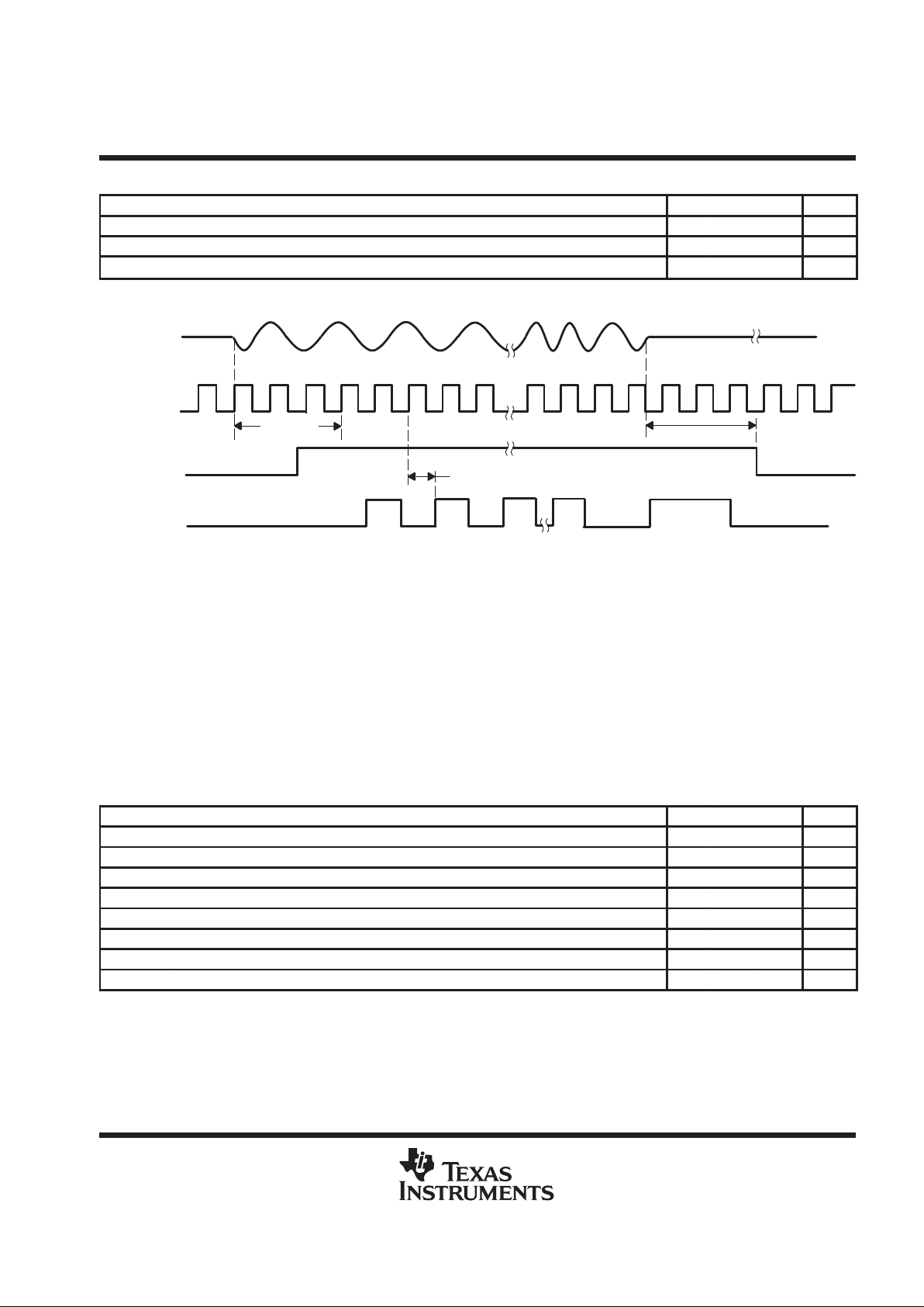
TNETE2004
MDIO-MANAGED QuadPHY
FOUR 10BASE-T PHYSICAL-LAYER INTERFACES
SPWS023D – OCTOBER 1996 – REVISED OCTOBER 1997
31
POST OFFICE BOX 655303 • DALLAS, TEXAS 75265
mode 4 receive-data timing
MIN TYP MAX UNIT
t
RDLAT
Receive-data latency 500 ns
t
PD
Receive data 40 60 ns
t
CRSHO
Time from receive idle to carrier sense off 200 ns
RCVP/
RCVN
RXCLK
(see Note A)
CRS
t
RDLAT
t
CRSHO
t
PD
RXD
(see Note B)
NOTES: A. RXCLK is continuous.
B. During a collision, the data output on RXD is not valid received data (or looped-back transmit data) since the digital PLL is acquiring
lock to a different source of incoming data.
Figure 21. Mode 4 Receive Timing
transmit-data timings
To be transmitted, data must be valid and synchronized with the appropriate edge of TXCLK according to the
selected compatibility mode (see T able 2). Figure 22 through Figure 25 show timing for modes of operation. The
only differences in modes are the polarity changes in RXD (during CRS deasserted), TXEN, RXCLK, and CRS.
In half-duplex operation, transmit data is internally looped back to the receive data pins through the receiver
circuitry. The following timing table shows transmit data timing.
modes 1–4 transmit-data timing
MIN TYP MAX UNIT
t
ENSU
Setup time, transmit enable 50 ns
t
SUD
Transmit startup delay 150 ns
t
CRSON
Time to CRS assertion 150 ns
t
TDSU
Setup time, transmit data 25 ns
t
TDHO
Hold time, transmit data 2.5 ns
t
TDLAT
Transmit-data latency 100 ns
t
TFIN
Time to transmit idle 400 ns
t
LOOP
Loopback latency 500 ns
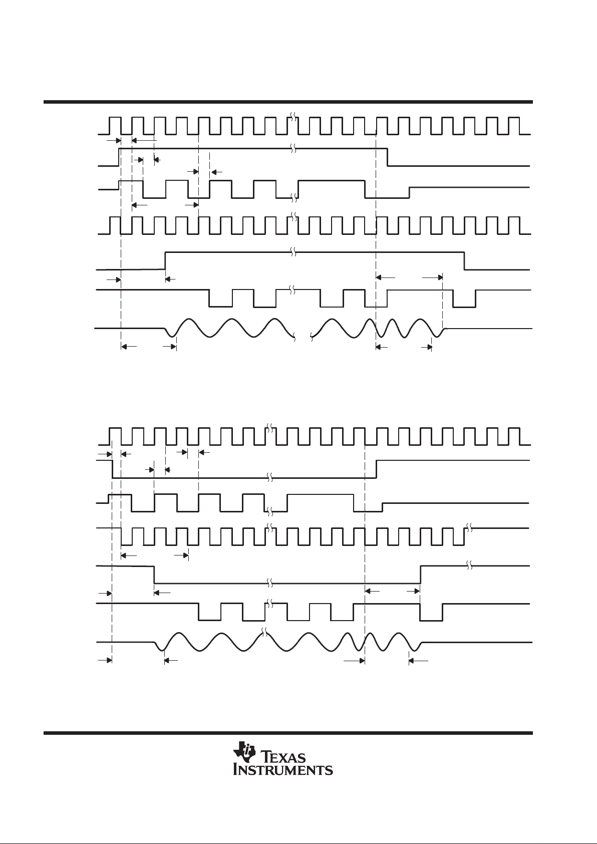
TNETE2004
MDIO-MANAGED QuadPHY
FOUR 10BASE-T PHYSICAL-LAYER INTERFACES
SPWS023D – OCTOBER 1996 – REVISED OCTOBER 1997
32
POST OFFICE BOX 655303 • DALLAS, TEXAS 75265
t
TDSU
XMTP/
XMTN
TXCLK
NOTES: A. RXCLK is continuous.
B. During a collision, the data output on RXD is not valid received data (or looped-back transmit data) since the digital PLL is acquiring
lock to a different source of incoming data.
TXEN
RXCLK
(see Note A)
CRS
TXD
RXD
(see Note B)
t
TFIN
t
CRSON
t
LOOP
t
TDHO
t
ENSU
t
TDLAT
t
SUD
Figure 22. Mode 1 Transmit Timing
t
TDSU
XMTP/
XMTN
TXCLK
NOTES: A. During a collision, the data output on RXD is not valid received data (or looped-back transmit data) since the digital PLL is acquiring
lock to a different source of incoming data.
B. RXCLK goes high seven clock cycles after CRS goes high.
TXEN
RXCLK
(see Note B)
CRS
TXD
RXD
(see Note A)
t
TFIN
t
CRSON
t
LOOP
t
TDHO
t
ENSU
t
TDLAT
t
SUD
Figure 23. Mode 2 Transmit Timing

TNETE2004
MDIO-MANAGED QuadPHY
FOUR 10BASE-T PHYSICAL-LAYER INTERFACES
SPWS023D – OCTOBER 1996 – REVISED OCTOBER 1997
33
POST OFFICE BOX 655303 • DALLAS, TEXAS 75265
t
ENSU
t
TDSU
XMTP/
XMTN
TXCLK
NOTES: A. During a collision, the data output on RXD is not valid received data (or looped-back transmit data) since the digital PLL is acquiring
lock to a different source of incoming data.
B. RXCLK goes high seven clock cycles after CRS goes low.
TXEN
RXCLK
(see Note B)
CRS
TXD
RXD
(see Note A)
t
TFIN
t
CRSON
t
LOOP
t
TDHO
t
TDLAT
t
SUD
Figure 24. Mode 3 Transmit Timing
t
ENSU
t
TDSU
XMTP/
XMTN
TXCLK
TXEN
RXCLK
(see Note A)
CRS
TXD
RXD
(see Note B)
t
TFIN
t
CRSON
t
LOOP
t
TDHO
t
TDLAT
t
SUD
NOTES: A. RXCLK is continuous.
B. During a collision, the data output on RXD is not valid received data (or looped-back transmit data) since the digital PLL is acquiring
lock to a different source of incoming data.
Figure 25. Mode 4 Transmit Timing

TNETE2004
MDIO-MANAGED QuadPHY
FOUR 10BASE-T PHYSICAL-LAYER INTERFACES
SPWS023D – OCTOBER 1996 – REVISED OCTOBER 1997
34
POST OFFICE BOX 655303 • DALLAS, TEXAS 75265
collision-detection timing
COL is asserted for a minimum of 600 ns when transmission and reception of data occur simultaneously . COL
is not active during link_fail or in full-duplex mode. Figure 26 through Figure 29 and the collision-detect timing
table show timing for modes of operation. Operation in all modes is identical except for polarity changes to TXEN
and COL. During a collision, the data output on RXD is not valid received data (or looped-back transmit data)
since the digital PLL is acquiring lock to a different source of incoming data.
collision-detect timing
MIN TYP MAX UNIT
t
COLON
Collision-detect delay 50 ns
t
COLOFF
Collision-off time 325 ns
t
COLON
COL
(see Note A)
RCVP/
RCVN
NOTE A: COL high in mode 1 asserts collision.
t
COLOFF
TXEN
Figure 26. Mode 1 Collision
t
COLON
COL
(see Note A)
RCVP/
RCVN
NOTE A: COL low in mode 2 asserts collision.
t
COLOFF
TXEN
Figure 27. Mode 2 Collision

TNETE2004
MDIO-MANAGED QuadPHY
FOUR 10BASE-T PHYSICAL-LAYER INTERFACES
SPWS023D – OCTOBER 1996 – REVISED OCTOBER 1997
35
POST OFFICE BOX 655303 • DALLAS, TEXAS 75265
t
COLON
COL
(see Note A)
RCVP/
RCVN
NOTE A: COL low in mode 3 asserts collision.
t
COLOFF
TXEN
Figure 28. Mode 3 Collision
t
COLON
COL
(see Note A)
RCVP/
RCVN
NOTE A: COL high in mode 4 asserts collision.
t
COLOFF
TXEN
Figure 29. Mode 4 Collision
absolute maximum ratings over operating free-air temperature range (unless otherwise noted)
†
Normal power-supply voltage 5.0 V ± 5%. . . . . . . . . . . . . . . . . . . . . . . . . . . . . . . . . . . . . . . . . . . . . . . . . . . . . . . . . .
Power-supply current draw (see Note 2) 510 mA. . . . . . . . . . . . . . . . . . . . . . . . . . . . . . . . . . . . . . . . . . . . . . . . . . .
Power-supply current draw (see Note 3) 240 mA. . . . . . . . . . . . . . . . . . . . . . . . . . . . . . . . . . . . . . . . . . . . . . . . . . .
dc voltage applied to logic outputs –0.05 V to V
CC
MAX. . . . . . . . . . . . . . . . . . . . . . . . . . . . . . . . . . . . . . . . . . . . .
dc voltage applied to logic input 5.25 V. . . . . . . . . . . . . . . . . . . . . . . . . . . . . . . . . . . . . . . . . . . . . . . . . . . . . . . . . . . .
dc differential voltage at receiver pins ± 5 V. . . . . . . . . . . . . . . . . . . . . . . . . . . . . . . . . . . . . . . . . . . . . . . . . . . . . . . .
Input voltage range (see Note 4) –0.5 V to 5.25 V. . . . . . . . . . . . . . . . . . . . . . . . . . . . . . . . . . . . . . . . . . . . . . . . . . .
Operating case temperature range, T
C
0°C to 95°C. . . . . . . . . . . . . . . . . . . . . . . . . . . . . . . . . . . . . . . . . . . . . . . .
R
θJA
(see Note 5) 22°C/W. . . . . . . . . . . . . . . . . . . . . . . . . . . . . . . . . . . . . . . . . . . . . . . . . . . . . . . . . . . . . . . . . . . . . . .
R
θJA
(see Note 6) 27°C/W. . . . . . . . . . . . . . . . . . . . . . . . . . . . . . . . . . . . . . . . . . . . . . . . . . . . . . . . . . . . . . . . . . . . . . .
Storage temperature range, T
stg
–65°C to 150°C. . . . . . . . . . . . . . . . . . . . . . . . . . . . . . . . . . . . . . . . . . . . . . . . . . .
†
Stresses beyond those listed under “absolute maximum ratings” may cause permanent damage to the device. These are stress ratings only, and
functional operation of the device at these or any other conditions beyond those indicated under “recommended operating conditions” is not
implied. Exposure to absolute-maximum-rated conditions for extended periods may affect device reliability.
NOTES: 2. With all PHYs transmitting and receiving (full duplex) into correctly terminated loads and inter-frame gaps of 9.6 ms
3. With all PHYs transmitting and receiving (full duplex) into correctly terminated loads and inter-frame gaps of 10 ms
4. Voltage values are with respect to GND, and all GND pins should be routed to minimize inductance to system ground.
5. 120 pin
6. 128 pin, 2.7-mm thickness

TNETE2004
MDIO-MANAGED QuadPHY
FOUR 10BASE-T PHYSICAL-LAYER INTERFACES
SPWS023D – OCTOBER 1996 – REVISED OCTOBER 1997
36
POST OFFICE BOX 655303 • DALLAS, TEXAS 75265
recommended operating conditions
MIN NOM MAX UNIT
V
CC
Supply voltage 4.75 5 5.25 V
V
SS
Supply voltage 0 V
p
All inputs except XTAL1 2 VCC +0.3
VIHHigh-level input voltage
XTAL1 2.8 VCC +0.3
V
V
IL
Low-level input voltage –0.3 0.8 V
recommended operating conditions
crystal oscillator
JEDEC
SYMBOL
TEST CONDITIONS MIN MAX UNIT
V
SB(XTL1)
Input self-bias voltage V
IB
1.7 2.8 V
I
OH(XTL2)
High-level output current I
OH
V
(XTL2)
= V
SB(XTL1)
V
(XTL1)
= V
SB(XTL1)
+ 0.5 V
–1.3 –5.0 mA
I
OL(XTL2)
Low-level output current I
OL
V
(XTL2)
= V
SB(XTL1)
V
(XTL1)
= V
SB(XTL1)
– 0.5 V
0.4 1.5 mA
recommended operating conditions
oscillator requirements
MIN TYP MAX UNIT
Oscillator, parallel resonant frequency 20 MHz
Oscillator, resonant frequency error –100 100 ppm
Oscillator, duty cycle 40 60 %

TNETE2004
MDIO-MANAGED QuadPHY
FOUR 10BASE-T PHYSICAL-LAYER INTERFACES
SPWS023D – OCTOBER 1996 – REVISED OCTOBER 1997
37
POST OFFICE BOX 655303 • DALLAS, TEXAS 75265
dc electrical characteristics over recommended ranges of supply voltage and operating free-air
temperature (see Figure 30)
PARAMETER
JEDEC
SYMBOL
TEST CONDITIONS MIN MAX UNIT
V
OH
High-level output voltage V
OH
VDD = min, IOH = –300mA 2.4 V
V
OL
Low-level output voltage V
OL
VDD = max, IOL = 2mA 0.5 V
V
OL,
see Note 7 High-level output voltage V
OL
VDD = max, IOL = 10mA 0.5 V
VOL, see Note 8 Low-level output voltage V
OL
VDD = max, IOL = 5mA 0.5 V
I
OZ
I
OZ
VDD = max, VO = VDD/V
SS
0 10 µA
I
I
I
I
VDD = max, VO = VDD/V
SS
10 µA
C
i
f = 1MHz 10 pF
C
o
f = 1MHz 10 pF
I
CCQ
VDD = max 100 µA
NOTES: 7. Maximum with LEDs on
8. Duplex pin
10BASE-T receiver input (RCVP, RCVN)
PARAMETER
JEDEC
SYMBOL
TEST CONDITIONS MIN MAX UNIT
V
(CM)
Common-mode input voltage V
IC
1.8 3.2 V
V
I(DIFF)
Differential input voltage V
ID
0.6 2.8 V
I
(CM)
Common-mode current I
IC
4 mA
V
SQ+
Rising input-pair squelch threshold VCM = VSB, See Note 9 270 mV
V
SQ–
Falling input-pair squelch threshold
VCM = VSB, See Note 9 –270 mV
NOTE 9: VSB is the self bias of the inputs RCVP and RCVN.
PLL characteristics
PARAMETER TEST CONDITIONS MIN MAX UNIT
V
FILT
Reference PLL operating filter voltage t
c(XTL1)
= 50 ns 0.8 2 V

TNETE2004
MDIO-MANAGED QuadPHY
FOUR 10BASE-T PHYSICAL-LAYER INTERFACES
SPWS023D – OCTOBER 1996 – REVISED OCTOBER 1997
38
POST OFFICE BOX 655303 • DALLAS, TEXAS 75265
PARAMETER MEASUREMENT INFORMATION
Outputs are driven to a minimum high-logic level of 2.4 V and to a maximum low-logic level of 0.6 V. These levels
are compatible with TTL devices.
Output transition times are specified as follows: For a high-to-low transition on either an input or output signal, the
level at which the signal no longer is considered high is 2 V . The level at which the signal is considered low is 0.8 V.
For a low-to-high transition, the level at which the signal no longer is considered low is 0.8 V , and the level at which
the signal is considered high is 2 V, as shown in the following diagram.
The rise and fall times are not specified but are assumed to be those of standard TTL devices, which are typically
1.5 ns.
2 V (high)
0.8 V (low)
test measurement
The test and load circuits shown in Figure 30 represent the programmable load of the tester-pin electronics used
to verify timing parameters of the TNETE2004 output signals.
(c) XMTP AND XMTN TEST LOAD (ac TESTING)
(b) IREF TEST CIRCUIT
(a) TTL OUTPUT TEST LOAD
180 Ω
IREF
C
L
I
OH
V
LOAD
I
OL
Test
Point
TTL
Output
Under
Test
Where: I
OH
= Refer to IOH in dc electrical characteristics.
I
OL
= Refer to IOL in dc electrical characteristics.
V
LOAD
= 1.5 V, typical dc-level verification or
0.7 V , typical timing verification
C
L
= 22 pF, typical load-circuit capacitance
50 Ω
50 Ω
Test
Point
Test
Point
XMTN
50 Ω
50 Ω
50 Ω
Test
Point
XMTN
XMTP
25 Ω
25 Ω
XMTP
50 Ω
X2
(d) XMTP AND XMTN TEST LOAD (dc TESTING)
X2–Fil–Mag 23Z128
ǒ
1: 2
Ǹ
Ǔ
Figure 30. Test and Load Circuit

TNETE2004
MDIO-MANAGED QuadPHY
FOUR 10BASE-T PHYSICAL-LAYER INTERFACES
SPWS023D – OCTOBER 1996 – REVISED OCTOBER 1997
39
POST OFFICE BOX 655303 • DALLAS, TEXAS 75265
APPLICATION INFORMATION
Interface of the TNETE2004 with the TNETX3150 and TNETX15VEPGE is shown in Figure 2. Details of that interface
are shown in Figure 31. Numbers and functions illustrated are for the 120-pin (PBE) device. Refer to
Terminal
Functions
table for corresponding pin numbers and functions for the 128-pin (PAC) device.

TNETE2004
MDIO-MANAGED QuadPHY
FOUR 10BASE-T PHYSICAL LAYER INTERFACES
SPWS023D – OCTOBER 1996 – REVISED OCTOBER 1997
T
emplate Release Date: 7–11–
94
40
POST OFFICE BOX 655303 DALLAS, TEXAS 75265
•
CRS0
2
1
COL0
117
1
LINK0
4
1
DUPLEX0
5
1
TXCLK
101
TXEN0
118
TXD0
119
RXCLK01RXD0
3
COL1
34
1
LINK1
27
1
DUPLEX1
26
1
TXEN1
33
1
TXD1
32
1
RXCLK1
31
1
RXD1
28
1
CRS1
29
1
RESET
15
1
LOOPBACK16AUTONEG74SQE
75
103
LED0LINK
109
LED1DUPCOL
99
MDCLK
100
MDIO
105
LED0ACTIVE
106
LED0DUPCOL
107
LED1LINK
108
LED1ACTIVE
9
XMTP0
18
XMTN1
23
RCVP1
22
RCVN1
8
XMTN0
13
RCVP0
12
RCVN0
19
XMTP1
95
DEVSEL296DEVSEL398DEVSEL4
XMT4+
XMT4–
M03_CRS
M03_COL
M03_LINK
M03_DPLX
TXCLK1
M03_TXEN
M03_TXD
M03_RCLK
M03_RXD
M04_COL
M04_LINK
M04_DPLX
M04_TXEN
M04_TXD
M04_RCLK
M04_RXD
M04_CRS
MRESET
LPBK
ANEG3–6
SQE3–6
11111
U2
TNETE2004
R5
6
COM1R12R23R34R4
5
M03_DPLX
M04_DPLX
23
23
4606X–101–103
RP3
10K
876
10
9
321
5
4
17
22
23
24
181920
21
25
303132
262728
29
333534
31
32
3840393637
111
1
1
1
XMT3_R+
XMT3_R–
RCV3+
RCV3–
XMT4_R+
XMT4_R–
XMT3+
XMT3–
RCV4+
RCV4–
MDIO
MDCLK
R1
R2
R3
5%
0.25 W
C1
+
+
C2 C3
C4
C5
C6 C7 C8 C9
50 V
10%
LNK3_DR
ACT3_DR
COL3_DR
LNK4_DR
ACT4_DR
COL4_DR
XMT4_P–
XMT4_P+
RCV4_P–
RCV4_P+
RCV3_P+
RCV3_P–
XMT3_P–
XMT3_P+
RJ45’S
J13
TG46–S010NX
T1
1:1
1:1
1: 2
1: 2
R9
49.9
1%
0.1 W
R8
49.9
1%
0.1 W
R10
49.9
1%
0.1 W
R11
49.9
1%
0.1 W
C10
50 V
10%
C11
50 V
10%
C12
100 pF
3000 V
10%
C13
100 pF
3000 V
10%
AGND1
AGND1
R4
24.9
1% 0.1 W
R5
24.9
1% 0.1 W
R6
24.9
1% 0.1 W
R7
24.9
1% 0.1 W
(RP3 IS OPTIONAL)
XMT4_COM
XMT3_COM
SIGNAL–GND: 6, 25, 35, 46, 49, 65, 84, 94, 97, 104, 115
SIGNAL–VCC: 30. 41, 52, 53, 60, 90, 102, 120
5%
0.25 W
5%
0.25 W
10 kΩ
V
CC
10 kΩ10 kΩ
0.1 µF
0.1 µF
.047 µF
50 V
10%
.047 µF
50 V
10%
.047 µF
50 V
10%
.047 µF
50 V
10%
.047 µF
50 V
10%
.047 µF
50 V
10%
.047 µF
10%
16 V
10%
10 µF
16 V
10 µF
V
CC
THIS IS THE ANALOG V
CC
TNETX15VEPGE/
TNETX15AEPGE/
TNETX315AL
Figure 31. QuadPHY-to-TNETX3150 Interface Diagrams

TNETE2004
MDIO-MANAGED QuadPHY
FOUR 10 BASE-T PHYSICAL LAYER INTERFACES
SPWS023D – OCTOBER 1996 – REVISED OCTOBER 1997
POST OFFICE BOX 655303 DALLAS, TEXAS 75265
• 41
COL2
56
1
LINK2
63
1
DUPLEX2
64
1
TXEN3
92
1
TXEN257TXD258RXCLK259RXD262CRS2
61
LINK3
86
1
DUPLEX3
85
1
TXD3
91
1
RXCLK3
89
1
RXD3
87
1
CRS3
88
1
COL3
93
1
TCK36TMS40TDI
37
110
LED2LINK
116
LED3DUPCOL
54
PWRDWN
55
RES1
111
LED2ACTIVE
112
LED2DUPCOL
113
LED3LINK
114
LED3ACTIVE
68
XMTP2
77
XMTN3
82
RCVP3
81
RCVN3
67
XMTN2
72
RCVP2
71
RCVN2
78
XMTP3
47
CMODE048CMODE1
44
ATEST
XMT6+
XMT6–
M05_COL
M05_DPLX
M06_TXEN
M05_TXEN
M05_TXD
M05_RCLK
M05_RXD
M05_CRS
M06_LINK
M06_DPLX
M06_TXD
M06_RCLK
M06_RXD
M06_CRS
M06_COL
GND
M05_LINK
11111
U2
TNETE2004
181716
20
19
13
12
11
15
14
1
6
7
8
234
5
9
141516
101112
13
232524
21
22
2830292627
111
1
1
1
XMT5_R+
XMT5_R–
RCV5+
RCV5–
XMT6_R–
XMT5+
XMT5–
RCV6+
RCV6–
C14
+
C15 C16
C17
C18
C19 C20 C21 C22
LNK5_DR
ACT5_DR
COL5_DR
LNK6_DR
ACT6_DR
COL6_DR
XMT6_P–
XMT6_P+
RCV6_P–
RCV6_P+
RCV5_P+
XMT5_P–
XMT5_P+
RJ45’S
J13
TG46–S010NX
T1
1:1
1:1
1: 2
1: 2
R21
49.9
1%
0.1 W
R20
49.9
1%
0.1 W
R22
49.9
1%
0.1 W
R23
49.9
1%
0.1 W
C25
50 V
10%
C26
50 V
10%
C27
100 pF
3000 V
10%
C28
100 pF
3000 V
10%
AGND1
AGND1
R12
24.9
1% 0.1 W
R17
24.9
1% 0.1 W
R18
24.9
1% 0.1 W
R19
24.9
1% 0.1 W
TDO38TRST39XTAL1
50
1
XTAL2
51
20MHZ_10A
L3
43
IREF
IREF1
ATST1
E1
R13
5%
.06 W
R14
5% .06 W
5% .06 W
R15
C23
50 V
10%
C24
16 V
R16
1% 0.1 W
178
AGND1
AGND1
AGND1AGND1
AGND1
AGND1
AGND1
AGND1
AGND1
AGND1
+
XMT6_R+
XMT6_COM
XMT5_COM
RCV5_P–
SIGNAL–AGND1: 7, 14, 17, 24, 45, 66, 73, 76, 83
SIGNAL–AVDD: 10, 11, 20, 21, 42, 69, 70, 79, 80
PWRDN1
AVDD
CMODE1–1
CMODE0–1
AGND1
0.1 µF
0.1 µF
10 kΩ
10 kΩ
THIS IS THE ANALOG V
CC
10%
0.1 µF
50 V
10%
0.1 µF
50 V
10%
0.1 µF
50 V
10%
0.1 µF
50 V
10%
0.1 µF
50 V
10%
0.1 µF
50 V
10%
0.1 µF
50 V
10%
0.1 µF
50 V
10%
0.1 µF
16 V
10%
10 µF
V
CC
V
CC
10 µF
10 kΩ
V
CC
V
CC
Figure 31. QuadPHY-to-TNETX3150 Interface Diagrams (Continued)

TNETE2004
MDIO-MANAGED QuadPHY
FOUR 10BASE-T PHYSICAL LAYER INTERFACES
SPWS023D – OCTOBER 1996 – REVISED OCTOBER 1997
T
emplate Release Date: 7–11–
94
42
POST OFFICE BOX 655303 DALLAS, TEXAS 75265
•
12
34
56
12
34
56
12
34
56
12
34
56
D1
D2
D3
D4
2
1
43658710912111413
2
1
43
6587109
121114
13
xxxx
xxxx
xxxx
xxxx
LNK3_DR
ACT3_DR
COL3_DR
LNK4_DR
ACT4_DR
COL4_DR
LNK5_DR
ACT5_DR
COL5_DR
LNK6_DR
ACT6_DR
COL6_DR
RP1
270
4614X–102–271
RP2
270
4614X–102–271
M03_RCLK
F1
2
M03_RXD
E1
2
M03_DPLX
E4
2
M03_LINK
E3
2
M03_TCLKG2M03_TXDG1M03_TXENF2M03_COLF4M03_CRS
F3
M04_RCLK
H1
2
M04_RXD
H2
2
M04_DPLX
G4
2
M04_LINK
G3
2
M04_TCLK
K1
2
M04_TXD
J1
2
M04_TXEN
J3
2
M04_COL
H4
2
M04_CRS
H3
2
M05_RCLK
K2
3
M05_RXD
L2
3
M05_DPLX
K4
3
M05_LINK
K3
3
M05_TCLK
M2
3
M05_TXD
M1
3
M05_TXEN
L1
3
M05_COL
L4
3
M05_CRS
L3
3
Y1
M07_TCLK
V1
M07_RCLK
V3
M07_RXD
U4
M07_DPLX
U3
M07_LINK
W1
M07_TXD
W2
M07_TXEN
W4
M07_COL
W3
M07_CRS
3
U2
M06_TCLK
3
R2
M06_RCLK
3
T2
M06_RXD
3
R4
M06_DPLX
3
R3
M06_LINK
3
U1
M06_TXD
3
T1
M06_TXEN
3
T4
M06_COL
3
T3
M06_CRS
AA1
M08_TCLK
Y3
M08_RCLK
Y2
M08_RXD
Y4
M08_DPLX
AA2
M08_LINK
AB1
M08_TXD
AB3
M08_TXEN
AA4
M08_COL
AA3
M08_CRS
TXCLK1
M06_RCLK
M06_RXD
M06_DPLX
M06_LINK
M06_TXD
M06_TXEN
M06_COL
M06_CRS
M03_RCLK
M03_RXD
M03_DPLX
M03_LINK
TXCLK1
M03_TXD
M03_TXEN
M03_COL
M03_CRS
M04_RCLK
M04_RXD
M04_DPLX
M04_LINK
TXCLK1
M04_TXD
M04_TXEN
M04_COL
M04_CRS
M05_RCLK
M05_RXD
M05_DPLX
M05_LINK
TXCLK1
M05_TXD
M05_TXEN
M05_COL
M05_CRS
3
33333
2
22222
22222
U1
TNETX3150
V
CC
Figure 31. QuadPHY-to-TNETX3150 Interface Diagrams (Continued)

TNETE2004
MDIO Managed QuadPHY
FOUR 10 BASE-T PHYSICAL LAYER INTERFACES
SPWS023D – OCTOBER 1996 – REVISED OCTOBER 1997
43
POST OFFICE BOX 655303 • DALLAS, TEXAS 75265
MECHANICAL DATA
PBE (S-PQFP-G120) PLASTIC QUAD FLATPACK
4040127/B 08/96
0,16 NOM
60
31
0,73
1,03
0,25
0,25 MIN
Seating Plane
Gage Plane
0,45
6190
0,30
91
120
SQ
SQ
31,45
27,80
28,20
30,95
23,20 TYP
3,60
3,20
4,10 MAX
130
0,10
0,80
M
0,20
0°–7°
NOTES: A. All linear dimensions are in millimeters.
B. This drawing is subject to change without notice.
C. Thermally enhanced molded plastic package with a heat spreader (HSP)
D. Falls within JEDEC MS-022

TNETE2004
MDIO Managed QuadPHY
FOUR 10 BASE-T PHYSICAL LAYER INTERFACES
SPWS023D – OCTOBER 1996 – REVISED OCTOBER 1997
44
POST OFFICE BOX 655303 • DALLAS, TEXAS 75265
MECHANICAL DATA
PAC (R-PQFP-G128) PLASTIC QUAD FLATPACK (DIE-DOWN)
4040274/B 03/95
0,15 NOM
18,0014,20
13,80 17,20
64
65
39
38
12,50 TYP
Heat Slug
1,10
0,70
0,25
Seating Plane
0,10 MIN
Gage Plane
0,30
0,10
102
1
18,50 TYP
103
128
24,00
23,20
19,80
20,20
3,10 MAX
2,70 TYP
0°–10°
0,10
0,50
M
0,08
NOTES: A. All linear dimensions are in millimeters.
B. This drawing is subject to change without notice.
C. Thermally enhanced molded plastic package (HSL) exposed on package bottom
D. Contact field sales office to determine if a tighter coplanarity requirement is available for this package.

TNETE2004
MDIO Managed QuadPHY
FOUR 10 BASE-T PHYSICAL LAYER INTERFACES
SPWS023D – OCTOBER 1996 – REVISED OCTOBER 1997
45
POST OFFICE BOX 655303 • DALLAS, TEXAS 75265
ORDERING INFORMATION
Packaging Option
PBE=120-pin PQFP
PAC=128-pin PQFP
Denotes PHY
Family Designator
E=Ethernet
Texas Instruments
Networking
Family Designator
PBE2ETNET 004
Denotes Quad

IMPORTANT NOTICE
T exas Instruments and its subsidiaries (TI) reserve the right to make changes to their products or to discontinue
any product or service without notice, and advise customers to obtain the latest version of relevant information
to verify, before placing orders, that information being relied on is current and complete. All products are sold
subject to the terms and conditions of sale supplied at the time of order acknowledgement, including those
pertaining to warranty, patent infringement, and limitation of liability.
TI warrants performance of its semiconductor products to the specifications applicable at the time of sale in
accordance with TI’s standard warranty. Testing and other quality control techniques are utilized to the extent
TI deems necessary to support this warranty. Specific testing of all parameters of each device is not necessarily
performed, except those mandated by government requirements.
CERT AIN APPLICATIONS USING SEMICONDUCTOR PRODUCTS MAY INVOL VE POTENTIAL RISKS OF
DEATH, PERSONAL INJURY, OR SEVERE PROPERTY OR ENVIRONMENTAL DAMAGE (“CRITICAL
APPLICATIONS”). TI SEMICONDUCTOR PRODUCTS ARE NOT DESIGNED, AUTHORIZED, OR
WARRANTED TO BE SUITABLE FOR USE IN LIFE-SUPPORT DEVICES OR SYSTEMS OR OTHER
CRITICAL APPLICATIONS. INCLUSION OF TI PRODUCTS IN SUCH APPLICA TIONS IS UNDERSTOOD T O
BE FULLY AT THE CUSTOMER’S RISK.
In order to minimize risks associated with the customer’s applications, adequate design and operating
safeguards must be provided by the customer to minimize inherent or procedural hazards.
TI assumes no liability for applications assistance or customer product design. TI does not warrant or represent
that any license, either express or implied, is granted under any patent right, copyright, mask work right, or other
intellectual property right of TI covering or relating to any combination, machine, or process in which such
semiconductor products or services might be or are used. TI’s publication of information regarding any third
party’s products or services does not constitute TI’s approval, warranty or endorsement thereof.
Copyright 1998, Texas Instruments Incorporated
 Loading...