


TMS320VC5421
DIGITAL SIGNAL PROCESSOR
SPRS098 – DECEMBER 1999
1
POST OFFICE BOX 1443 • HOUSTON, TEXAS 77251–1443
D 200-MIPS Dual-Core DSP Consisting of Two
Independent Subsystems
D Each Core Has an Advanced Multibus
Architecture With Three Separate 16-Bit
Data Memory Buses and One Program Bus
D 40-Bit Arithmetic Logic Unit (ALU)
Including a 40-Bit Barrel-Shifter and Two
40-Bit Accumulators Per Core
D Each Core Has a 17-Bit × 17-Bit Parallel
Multiplier Coupled to a 40-Bit Adder for
Non-Pipelined Single-Cycle Multiply/
Accumulate (MAC) Operations
D Each Core Has a Compare, Select, and
Store Unit (CSSU) for the Add/Compare
Selection of the Viterbi Operator
D Each Core Has an Exponent Encoder to
Compute an Exponent Value of a 40-Bit
Accumulator Value in a Single Cycle
D Each Core Has Two Address Generators
With Eight Auxiliary Registers and Two
Auxiliary Register Arithmetic Units
(ARAUs)
D 16-Bit Data Bus With Data Bus Holder
Feature
D 512K-Word × 16-Bit Extended Program
Address Space
D Total of 256K-Word × 16-Bit Dual- and
Single-Access On-Chip RAM (128K-Word x
16-Bit Shared Memory)
D Single-Instruction Repeat and
Block-Repeat Operations
D Instructions With 32-Bit-Long Word
Operands
D Instructions With 2 or 3 Operand Reads
D Fast Return From Interrupts
D Arithmetic Instructions With Parallel Store
and Parallel Load
D Conditional Store Instructions
D Output Control of CLKOUT
D Output Control of TOUT
D Power Consumption Control With IDLE1,
IDLE2, and IDLE3 Instructions
D Dual 1.8-V (Core) and 3.3-V (I/O) Power
Supplies for Low-Power, Fast Operations
D 10-ns Single-Cycle Fixed-Point Instruction
D Interprocessor Communication via Two
Internal 8-Element FIFOs
D Twelve Channels of Direct Memory Access
(DMA) for Data Transfers With No CPU
Loading (Six Channels Per Subsystem With
External Access)
D Six Multichannel Buffered Serial Ports
(McBSPs) With 128-Channel Selection
Capability (3 McBSPs per Subsystem)
D 16-Bit Host-Port Interface (HPI) Multiplexed
With External Memory Interface Pins
D Software-Programmable Phase-Locked
Loop (APLL) Provides Several Clocking
Options (Requires External TTL Oscillator)
D Includes JTAG Functionality for In-Circuit
Emulation
D On-Chip Scan-Based Emulation Logic,
IEEE Standard 1149-1
{
(JTAG) Boundary-
Scan Logic
D T wo Software-Programmable Timers
(One Per Subsystem)
D Software-Programmable Wait-State
Generator (14 Wait States Maximum)
D Provided in 144-pin MicroStart Ball Grid
Array (GGU Suffix) and 144-pin Thin Quad
Flatpack (TQFP) (PGE Suffix) Packages
description
The TMS320VC5421 fixed-point digital signal processor (DSP) is a dual-core solution running at 200-MIPS
performance. The ’5421 consists of two DSP subsystems capable of core-to-core communications and a
128K-word zero-wait-state on-chip program memory shared by the two DSP subsystems. Each subsystem
consists of one ’54x DSP core, 32K-word program/data DARAM, 32K-word data SARAM, 2K-word ROM, three
multichannel serial interfaces, xDMA logic, one timer, one APLL, and other miscellaneous circuitry.
ADVANCE
INFORMATION
Copyright 1999, Texas Instruments Incorporated
ADVANCE INFORMATION concerns new products in the sampling or
preproduction phase of development. Characteristic data and other
specifications are subject to change without notice.
Please be aware that an important notice concerning availability, standard warranty, and use in critical applications of
Texas Instruments semiconductor products and disclaimers thereto appears at the end of this data sheet.
MicroStar is a trademark of Texas Instruments Incorporated.
†
IEEE Standard 1149.1-1990, IEEE Standard Test-Access Port and Boundary Scan Architecture.

TMS320VC5421
DIGITAL SIGNAL PROCESSOR
SPRS098 – DECEMBER 1999
2
POST OFFICE BOX 1443 • HOUSTON, TEXAS 77251–1443
description (continued)
The ’5421 also contains a host-port interface (HPI) that allows the ’5421 to be viewed as a memory-mapped
peripheral to a host processor. The ’5421 is pin-compatible with the TMS320VC5420.
Each subsystem has its separate program and data spaces, allowing simultaneous accesses to program
instructions and data. Two read operations and one write operation can be performed in one cycle. Instructions
with parallel store and application-specific instructions can fully utilize this architecture. Furthermore, data can
be transferred between program and data spaces. Such parallelism supports a powerful set of arithmetic, logic,
and bit-manipulation operations that can all be performed in a single machine cycle. The ’5421 includes the
control mechanisms to manage interrupts, repeated operations, and function calls. In addition, the ’5421 has
128K words of on-chip program memory that can be shared between the two subsystems.
The ’5421 is intended as a high-performance, low-cost, high-density DSP for remote data access or voice-over
IP subsystems. It is designed to maintain the current modem architecture with minimal hardware and software
impacts, thus maximizing reuse of existing modem technologies and development efforts.
NOTE: This data sheet is designed to be used in conjunction with the
TMS320C5000 DSP Family Functional
Overview
(literature number SPRU307).
migration from the ’5420 to the ’5421
Customers who are migrating from the ’5420 to the ’5421 need to take into account the following differences
between the two devices.
The memory structure of the ’5421 has been changed to incorporate 128K x 16-bit words of shared memory .
The DMA of the ’5421 has been enhanced to provide access to external, as well as internal memory.
The HPI and DMA memory maps have been changed to incorporate the new memory ’5421.
2K x 16-bit words of ROM have been added to the ’5421 for bootloading purposes only.
The VCO pin on the ’5420 has been replaced with the HOLDA pin on the ’5421 and the HOLD pin was added
to the ’5421 at a previously unused pin location.
The McBSPs have been updated with a new mode that allows 128-channel selection capability.
McBSP CLKX/R pins can be used as inputs to internal clock rate generator for CLKS-like function without
the penalty of extra pins.
The SELA/B pin on ’5421 is changed to type I/O/Z for added functionality.
NOTE: For more detailed information, see the 5420 to 5421 migration issues document .
ADVANCE
INFORMATION
TMS320VC5421
DIGITAL SIGNAL PROCESSOR
SPRS098 – DECEMBER 1999
3
POST OFFICE BOX 1443 • HOUSTON, TEXAS 77251–1443
AV
PPA14
PPA15
V
SS
PPA16
PPA17
B_INT0
B_INT1
B_NMI
IS
B_GPIO2/BIO
B_GPIO1
B_GPIO0
B_BFSR1
B_BDR1
CV
DD
V
SS
B_BCLKR1
B_BFSX1
V
SS
B_BDX1
B_BCLKX1
CV
DD
V
SS
TEST
XIO
B_RS
B_XF
B_CLKOUT
HMODE
HPIRS
PPA13
PPA12
V
SS
DV
DD
PPA11
PPA10
PPD7
PPA8
PPA0
DV
DD
PPA9
PPD1
A_INT1
A_NMI
IOSTRB
A_GPIO2/BIO
A_GPIO1
A_RS
A_GPIO0
V
SS
V
SS
CV
DD
A_BFSR1
A_BDR1
A_BCLKR1
A_BFSX1
CV
DD
V
SS
A_BDX1
A_BCLKX1
A_XF
A_CLKOUT
HOLDA
TCK
TMS
TDI
TRST
EMU1/OFF
DV
DD
A_INT0
EMU0
TDO
144
PPD0
PPD5
143
142
141
PPD6
140
A_BFSX2
139
A_BDX2
138
A_BFSR2
137
A_BDR2
136
A_BCLKR2
135
134
133
A_BCLKX2
132
READY
131DV130
129
128
127
126
125
B_BCLKX2
124
B_BDX2
123
B_BFSX2
122
B_BCLKR2
121
120
119
B_BDR2
118
117
PPD2
116
PPD3
115
PPA1
114
PPA5
113
112
373839404142434445464748495051525354555657585960616263646566676869
1
2
3
4
5
6
7
8
9
10
11
12
13
14
15
16
17
18
19
20
21
22
23
24
25
26
27
28
29
30
31
32
33
34
35
36
108
107
106
105
104
103
102
101
100
99
98
97
96
95
94
93
92
91
90
89
88
87
86
85
84
83
82
81
80
79
78
77
76
75
74
73
PPD15
PPD14SSPPD13
PPD12
A_BFSR0
A_BDR0
A_BCLKR0
A_BFSX0
A_BDX0
A_BCLKX0
DD
SS
B_BFSX0
B_BCLKR0
B_BDR0
B_BFSR0
R/W
PPA2
PPA3
SELA/B
PPD8
PPD9
PPD10
B_BDX0
MSTRB
111
110
PPA7
109
707172
PPD11
B_BFSR2
PPA6
DV
CLKIN
V
DV
V
DD
DD
DD
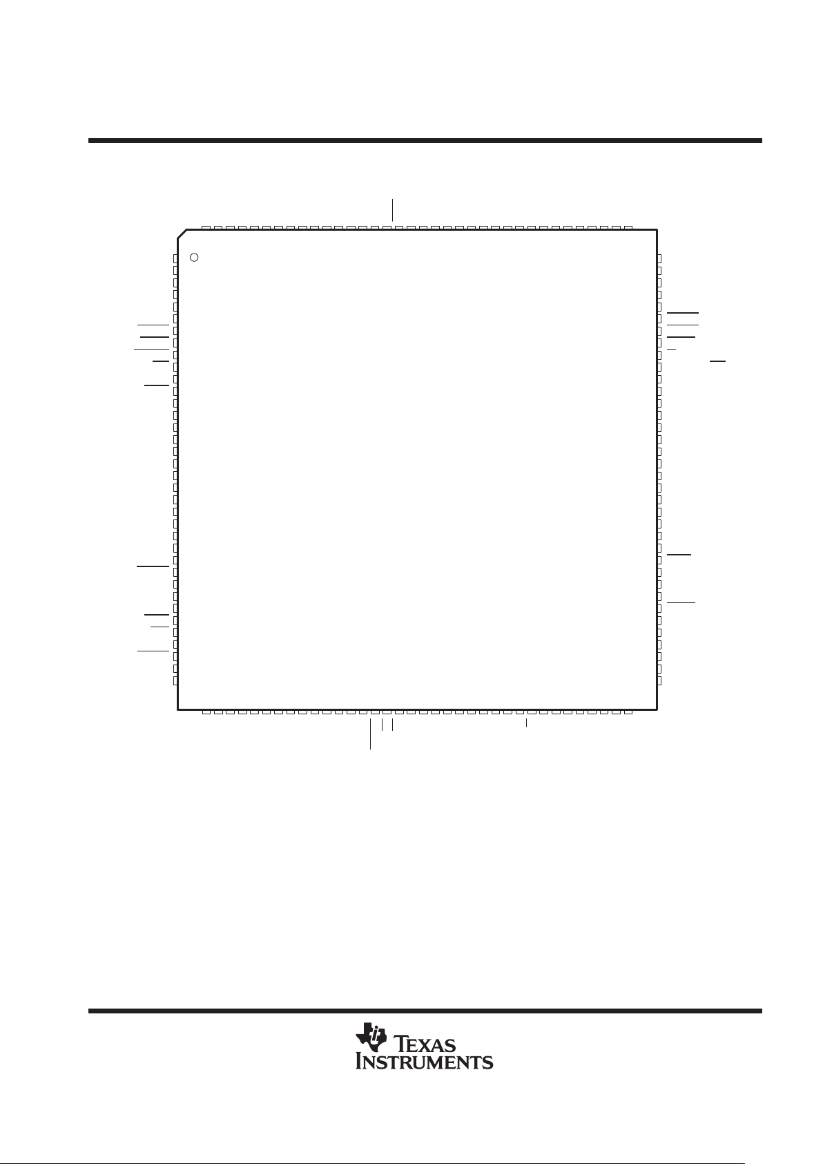
PGE PACKAGE
†‡
(TOP VIEW)
PPD4
B_BCLKX0
SS
V
V
SS
SS
V
SS
V
SS
V
DD
CV
DS
PS
DD
CV
SS
V
PPA4
SS
V
CV
DD
SSA
V
HOLD
CV
DD
SS
V
†
DVDD is the power supply for the I/O pins while CVDD is the power supply for the core CPU. VSS is the ground for both the I/O pins and the core
CPU.
‡
Pin configuration shown for nonmultiplexed mode only. See the pin assignments table for the TMS320VC5421PGE for multiplexed functions of
specific pins and for specific pin numbers.
The TMS320VC5421PGE 144-pin thin quad flatpack (TQFP) is footprint- and pin-compatible with the ’5420.
ADVANCE
INFORMATION
TMS320VC5421
DIGITAL SIGNAL PROCESSOR
SPRS098 – DECEMBER 1999
4
POST OFFICE BOX 1443 • HOUSTON, TEXAS 77251–1443
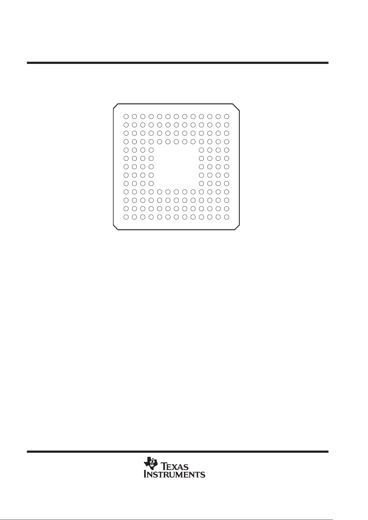
GGU PACKAGE
(BOTTOM VIEW)
A
B
D
C
E
F
H
J
L
M
K
N
G
12
3456781012 1113 9
The pin assignments table for the TMS320VC5421GGU lists each pin name and its associated pin number for
this 144-pin ball grid array (BGA) package, which is footprint- and pin-compatible with the ’5420.
The signal descriptions table lists each pin name, function, and operating mode(s) for the ’5421 device.
ADVANCE
INFORMATION
TMS320VC5421
DIGITAL SIGNAL PROCESSOR
SPRS098 – DECEMBER 1999
5
POST OFFICE BOX 1443 • HOUSTON, TEXAS 77251–1443
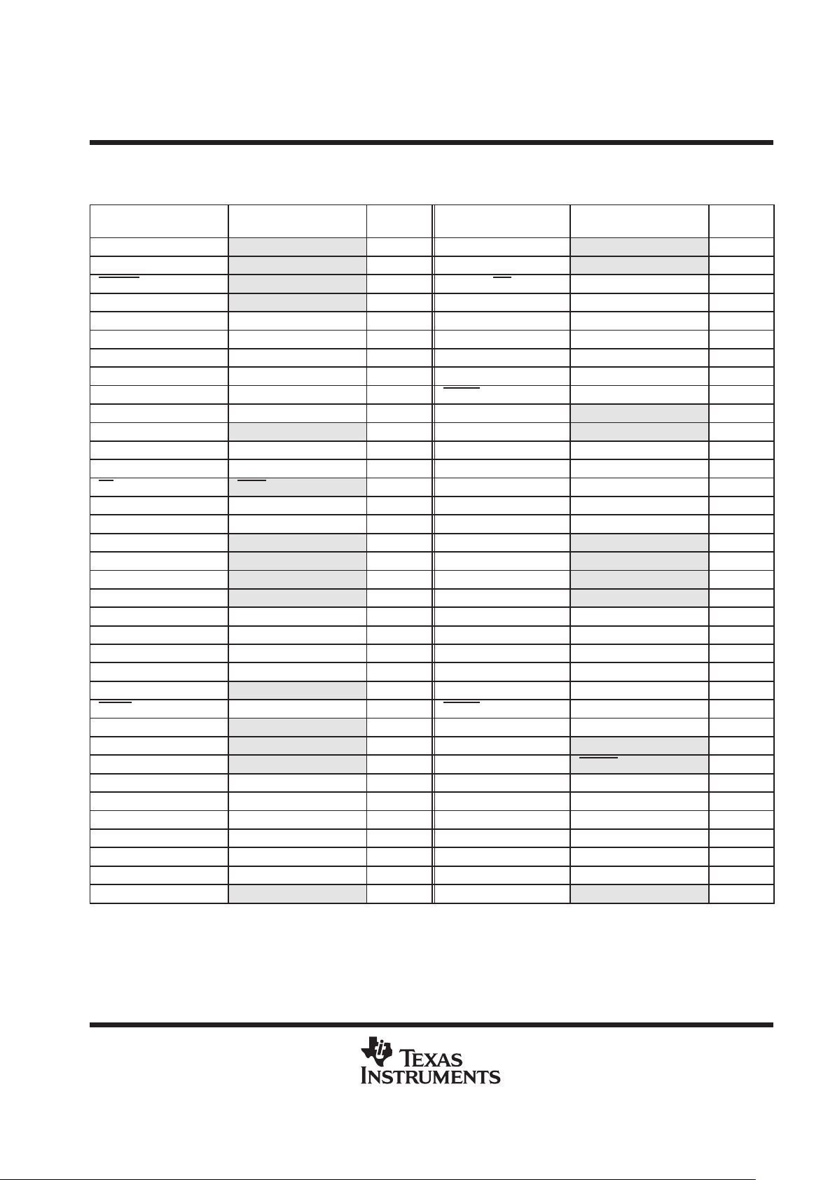
Pin Assignments for the TMS320VC5421PGE
(144-Pin Thin Quad Flatpack)
SIGNAL NAME
(NONMULTIPLEXED)
SIGNAL NAME
(MULTIPLEXED)
PIN
NO.
SIGNAL NAME
(NONMULTIPLEXED)
SIGNAL NAME
(MULTIPLEXED)
PIN
NO.
PPD7 HD7 1 PPA8 HA8 2
PPA9 HA9 5 PPD1 HD1 6
IOSTRB A_GPIO3/A_TOUT 9 A_GPIO2/BIO 10
A_GPIO0 A_ROMEN 13 V
SS
14
A_BFSR1 17 A_BDR1 18
CV
DD
21 V
SS
22
A_XF 25 A_CLKOUT 26
TMS 29 TDI 30
DV
DD
33 A_INT0 34
V
SS
37 PPD15 HD15 38
PPD13 HD13 41 PPD12 HD12 42
A_BCLKR0 45 A_BFSX0 46
A_BDX0 49 A_BCLKX0 50
PS HDS1 53 B_BCLKX0 54
V
SS
57 B_BFSX0 58
CV
DD
61 V
SS
62
PPA2 HCNTL1/HA2 65 PPA3 HCNTL0/HA3 66
PPD9 HD9 69 PPD10 HD10 70
PPA10 HA10 73 PPA11 HA11 74
PPA12 HA12 77 PPA13 HA13 78
B_CLKOUT 81 B_XF 82
TEST 85 V
SS
86
B_BDX1 89 V
SS
90
V
SS
93 CV
DD
94
B_GPIO0 B_ROMEN 97 B_GPIO1 98
B_NMI 101 B_INT1 102
PPA16 HA16 105 V
SS
106
PPA7 HA7 109 PPA6 HA6 110
PPA5 HA5 113 PPA1 B_HINT/HA1 114
B_BFSR2 117 B_BDR2 118
B_BCLKR2 121 B_BFSX2 122
V
SS
125 AV
DD
126
CLKIN 129 DV
DD
130
CV
DD
133 V
SS
134
A_BFSR2 137 A_BDX2 138
PPD4 HD4 141 PPD5 HD5 142
ADVANCE
INFORMATION
TMS320VC5421
DIGITAL SIGNAL PROCESSOR
SPRS098 – DECEMBER 1999
6
POST OFFICE BOX 1443 • HOUSTON, TEXAS 77251–1443
Pin Assignments for the TMS320VC5421PGE
(144-Pin Thin Quad Flatpack) (Continued)
SIGNAL NAME
(NONMULTIPLEXED)
SIGNAL NAME
(MULTIPLEXED)
PIN
NO.
SIGNAL NAME
(NONMULTIPLEXED)
SIGNAL NAME
(MULTIPLEXED)
PIN
NO.
PPA0 A_HINT/HA0 3 DV
DD
4
A_INT1 7 A_NMI 8
A_GPIO1 11 A_RS 12
V
SS
15 CV
DD
16
A_BCLKR1 19 A_BFSX1 20
A_BDX1 23 A_BCLKX1 24
HOLDA 27 TCK 28
TRST 31 EMU1/OFF 32
EMU0 35 TDO 36
PPD14 HD14 39 V
SS
40
A_BFSR0 43 A_BDR0 44
V
SS
47 CV
DD
48
MSTRB HCS 51 DS HDS2 52
B_BDX0 55 DV
DD
56
B_BCLKR0 59 B_BDR0 60
B_BFSR0 63 R/W HR/W 64
SELA/B PPA18 67 PPD8 HD8 68
PPD11 HD11 71 V
SS
72
DV
DD
75 V
SS
76
HPIRS 79 HMODE 80
B_RS 83 XIO 84
CV
DD
87 B_BCLKX1 88
B_BFSX1 91 B_BCLKR1 92
B_BDR1 95 B_BFSR1 96
B_GPIO2/BIO 99
IS
B_GPIO3/B_TOUT
100
B_INT0 103 PPA17 HA17 104
PPA15 HA15 107 PPA14 HA14 108
PPA4 HAS/HA4 111 DV
DD
112
PPD3 HD3 115 PPD2 HD2 116
V
SS
119 CV
DD
120
B_BDX2 123 B_BCLKX2 124
V
SSA
127 HOLD 128
READY HRDY 131 A_BCLKX2 132
A_BCLKR2 135 A_BDR2 136
A_BFSX2 139 PPD6 HD6 140
PPD0 HD0 143 V
SS
144
ADVANCE
INFORMATION
TMS320VC5421
DIGITAL SIGNAL PROCESSOR
SPRS098 – DECEMBER 1999
7
POST OFFICE BOX 1443 • HOUSTON, TEXAS 77251–1443
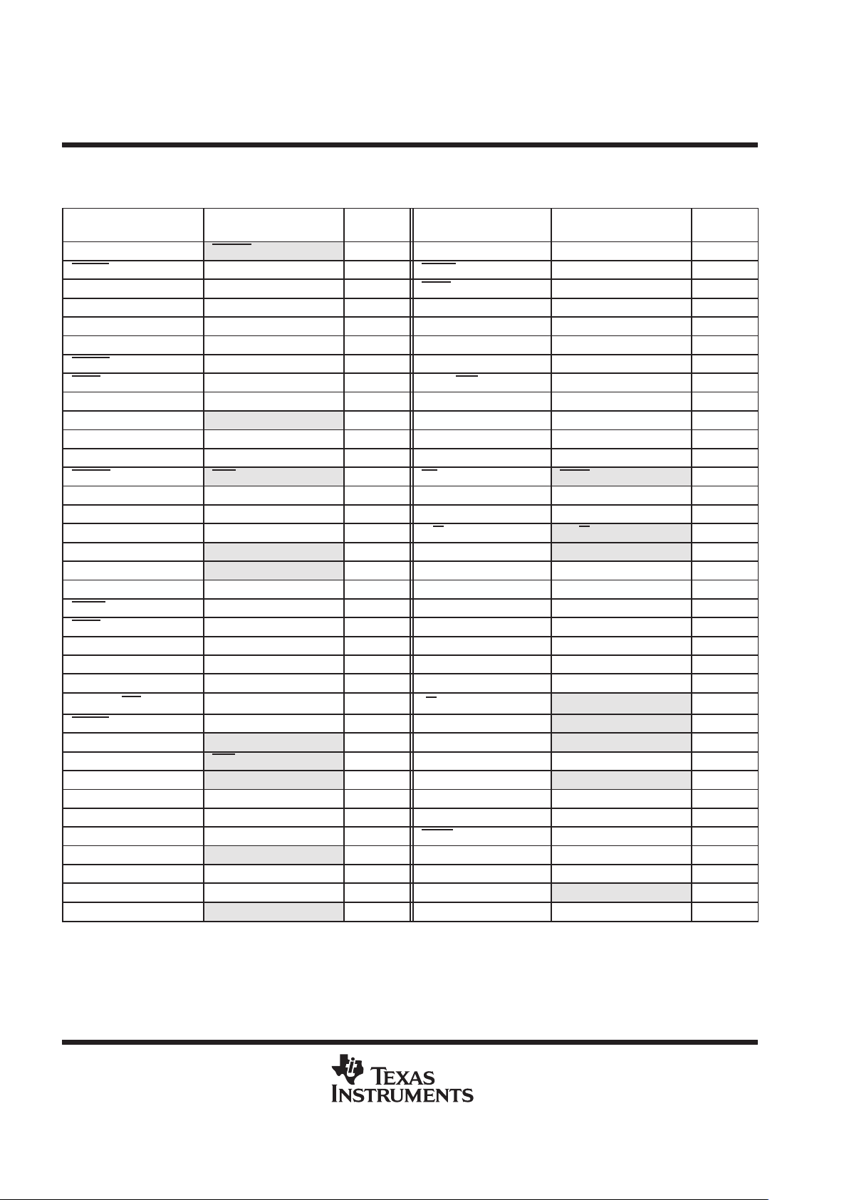
Pin Assignments for the TMS320VC5421GGU
(144-Pin MicroStar Ball Grid Array)
SIGNAL NAME SIGNAL NAME BALL SIGNAL NAME SIGNAL NAME BALL
(NONMULTIPLEXED) (MULTIPLEXED) NO. (NONMULTIPLEXED) (MULTIPLEXED) NO.
PPD7 HD7 A1 PPA8 HA8 B1
A_RS E1 CV
DD
F1
A_XF J1 TMS K1
V
SS
N1 PPD0 HD0 A2
A_INT1 D2 A_GPIO1 E2
V
SS
H2 A_CLKOUT J2
TDO M2 PPD15 HD15 N2
PPD5 HD5 C3 PPD1 HD1 D3
A_BCLKR1 G3 A_BDX1 H3
A_INT0 L3 PPD14 HD14 M3
A_BDX2 B4 A_BFSX2 C4
A_GPIO0 A_ROMEN F4 A_BFSX1 G4
PPD13 HD13 K4 PPD12 HD12 L4
CV
DD
A5 V
SS
B5
A_BCLKR0 K5 A_BFSX0 L5
CLKIN A6 DV
DD
B6
A_BDX0 K6 A_BCLKX0 L6
AV
DD
A7 V
SS
B7
DV
DD
K7 B_BDX0 L7
B_BCLKX2 A8 B_BDX2 B8
B_BDR0 K8 B_BCLKR0 L8
CV
DD
A9 V
SS
B9
R/W HR/W K9 B_BFSR0 L9
PPD2 HD2 A10 PPD3 HD3 B10
IS B_GPIO3/B_TOUT E10 B_BFSR1 F10
B_CLKOUT J10 PPA12 HA12 K10
PPA2 HCNTL1/HA2 N10 DV
DD
A11
B_INT0 D11 B_GPIO2/BIO E11
V
SS
H11 B_XF J11
PPD9 HD9 M11 PPD8 HD8 N11
PPA16 HA16 C12 B_INT1 D12
B_BDX1 G12 CV
DD
H12
DV
DD
L12 V
SS
M12
PPA15 HA15 B13 PPA17 HA17 C13
V
SS
F13 V
SS
G13
HMODE K13 V
SS
L13
ADVANCE
INFORMATION
TMS320VC5421
DIGITAL SIGNAL PROCESSOR
SPRS098 – DECEMBER 1999
8
POST OFFICE BOX 1443 • HOUSTON, TEXAS 77251–1443
Pin Assignments for the TMS320VC5421GGU
(144-Pin MicroStar Ball Grid Array) (Continued)
SIGNAL NAME SIGNAL NAME BALL SIGNAL NAME SIGNAL NAME BALL
(NONMULTIPLEXED) (MULTIPLEXED) NO. (NONMULTIPLEXED) (MULTIPLEXED) NO.
DV
DD
C1 A_NMI D1
A_BDR1 G1 CV
DD
H1
EMU1/OFF L1 EMU0 M1
V
SS
B2 PPA0 A_HINT/HA0 C2
V
SS
F2 A_BFSR1 G2
TDI K2 DV
DD
L2
PPD6 HD6 A3 PPD4 HD4 B3
A_GPIO2/BIO E3 V
SS
F3
HOLDA J3 TRST K3
V
SS
N3 A_BFSR2 A4
PPA9 HA9 D4 IOSTRB A_GPIO3/A_TOUT E4
A_BCLKX1 H4 TCK J4
A_BFSR0 M4 A_BDR0 N4
A_BCLKR2 C5 A_BDR2 D5
V
SS
M5 CV
DD
N5
READY HRDY C6 A_BCLKX2 D6
MSTRB HCS M6 DS HDS2 N6
V
SSA
C7 HOLD D7
PS HDS1 M7 B_BCLKX0 N7
B_BFSX2 C8 B_BCLKR2 D8
B_BFSX0 M8 V
SS
N8
B_BDR2 C9 B_BFSR2 D9
V
SS
M9 CV
DD
N9
PPA1 B_HINT/HA1 C10 PPA5 HA5 D10
B_BCLKR1 G10 TEST H10
SELA/B PPA18 L10 PPA3 HCNTL0/HA3 M10
PPA4 HAS/HA4 B11 V
SS
C11
B_BDR1 F11 B_BFSX1 G11
PPA13 HA13 K11 PPD10 HD10 L11
PPA6 HA6 A12 PPA14 HA14 B12
B_GPIO1 E12 CV
DD
F12
B_RS J12 HPIRS K12
PPD11 HD11 N12 PPA7 HA7 A13
B_NMI D13 B_GPIO0 B_ROMEN E13
B_BCLKX1 H13 XIO J13
PPA11 HA11 M13 PPA10 HA10 N13
ADVANCE
INFORMATION
TMS320VC5421
DIGITAL SIGNAL PROCESSOR
SPRS098 – DECEMBER 1999
9
POST OFFICE BOX 1443 • HOUSTON, TEXAS 77251–1443
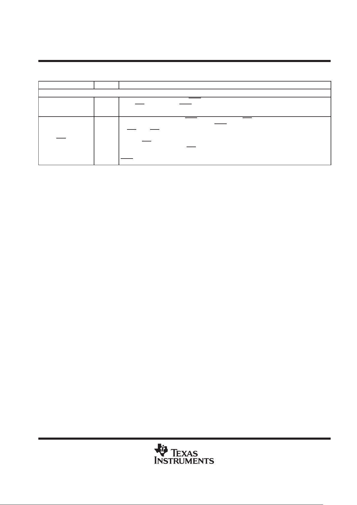
Signal Descriptions
NAME TYPE
†
DESCRIPTION
DATA SIGNALS
PPA18 (MSB)
PPA17
PPA16
PPA15
PPA14
PPA13
PPA12
PPA11
PPA10
PPA9
PPA8
PPA7
PPA6
PPA5
PPA4
‡§
PPA3
PPA2
PPA1
PPA0 (LSB)
I/O/Z
Parallel port address bus. The DSP can access the external memory locations by way of the external
memory interface using PPA[18:0] in external memory interface (EMIF) mode when the XIO pin is logic
high. PPA18 is a secondary output function of the SELA/B pin.
The PPA[17:0] pins are also multiplexed with the HPI interface. In HPI mode (XIO pin is low), the external
address pins PPA[17:0] are used by a host processor for access to the memory map by way of the
on-chip HPI. Refer to the Host-Port Interface (HPI) Signals section of this table for details on the
secondary functions of these pins.
These pins are placed into the high-impedance state when OFF
is low.
PPD15 (MSB)
PPD14
PPD13
PPD12
PPD11
PPD10
PPD9
PPD8
PPD7
PPD6
PPD5
PPD4
PPD3
PPD2
PPD1
PPD0 (LSB)
I/O/Z
¶
Parallel port data bus. The DSP uses this bidirectional data bus to access external memory when the
device is in external memory interface (EMIF) mode (the XIO pin is logic high).
This data bus is also multiplexed with the 16-bit HPI data bus. When in HPI mode, the bus is used to
transfer data between the host processor and internal DSP memory via the HPI. Refer to the HPI section
of this table for details on the secondary functions of these pins.
The data bus includes bus holders to reduce power dissipation caused by floating, unused pins. The bus
holders also eliminate the need for external pullup resistors on unused pins. When the data bus is not
being driven by the ’5421, the bus holders keep data pins at the last driven logic level. The data bus
keepers are disabled at reset and can be enabled/disabled via the BH bit of the BSCR register.
These pins are placed into high-impedance state when OFF
is low.
INITIALIZATION, INTERRUPT, AND RESET OPERATIONS
A_INT0
§
B_INT0
§
A_INT1
§
B_INT1
§
I
External user interrupts. A_INT0–B_INT0 are prioritized and are maskable by the interrupt mask register
(IMR) and the interrupt mode bit. A_INT1
–B_INT1 can be polled and reset by way of the interrupt flag
register (IFR).
A_NMI
§
B_NMI
§
I
Nonmaskable interrupt. NMI is an external interrupt that cannot be masked by way of the INTM or the
IMR. When NMI
is activated, the processor traps to the appropriate vector location.
A_RS
§
B_RS
§
I
Reset. RS causes the digital signal processor (DSP) to terminate execution and causes a reinitialization
of the CPU and peripherals. When RS
is brought to a high level, execution begins at location 0FF80h
of program memory. RS
affects various registers and status bits.
†
I = Input, O = Output, S = Supply, Z = High Impedance
‡
This pin has an internal pullup resistor.
§
These pins are Schmitt triggered inputs.
¶
This pin has an internal bus holder controlled by way of the BSCR register in 54x cLEAD core of DSP subsystem A .
#
This pin is used by Texas Instruments for device testing and should be left unconnected.
||
This pin has an internal pulldown resistor.
ADVANCE
INFORMATION
TMS320VC5421
DIGITAL SIGNAL PROCESSOR
SPRS098 – DECEMBER 1999
10
POST OFFICE BOX 1443 • HOUSTON, TEXAS 77251–1443
Signal Descriptions (Continued)
NAME DESCRIPTIONTYPE
†
INITIALIZATION, INTERRUPT, AND RESET OPERATIONS (CONTINUED)
XIO I
The XIO pin is used to configure the parallel port as a host-port interface (HPI mode when XIO pin is low),
or as an asynchronous memory interface (EMIF mode when XIO pin is high).
At device reset, the XIO pin level determines the initialization value of the MP/MC bit (a bit in the
processor mode status (PMST) register). Refer to the memory section for details.
GENERAL-PURPOSE I/O PINS
A_XF
B_XF
O/Z
External flag output (latched software-programmable output-only signal). Bit-addressable. A_XF and
B_XF are placed into the high-impedance state when OFF
is low.
A_GPIO0
A_ROMEN
General-purpose I/O pins. The secondary function of these pins. In XIO mode,
p
pp
p
A_GPIO0
B_GPIO0
I/O/Z
B_ROMEN
I
the ROM enable (ROMEN) pins are used to enable the applicable on-chip ROM
after reset.
A_GPIO1
B_GPIO1
I/O/Z
General-purpose I/O pins (software-programmable I/O signal). Values can be latched (output) by
writing into the GPIO register. The states of GPIO pins (inputs) can be read by reading the GPIO
register. The GPIO direction is also programmable by way of the DIRn field in the GPIO register.
A_GPIO2/BIO
B_GPIO2/BIO
I/O/Z
General-purpose I/O. These pins can be configured like GPIO0–GPIO1; however, as an input, the pins
operate as the traditional branch control bit (BIO
). If application code does not perform BIO-conditional
instructions, these pins operate as general inputs.
PRIMARY
A_GPIO3
(A_TOUT)
IOSTRB
When the device is in HPI mode and HMODE = 0 (multiplexed), these pins act
according to the general-purpose I/O control register. TOUT bit must be set to “1”
B_GPIO3
(B_TOUT)
I/O/Z
IS
O
to drive the timer output on the pin. IF TOUT = 0, then these pins are
general-purpose I/Os. In EMIF mode (XIO = 1), these signals are active during
I/O space accesses.
MEMORY CONTROL SIGNALS
PS
‡§
Program space select signal. The PS signal is asserted during external program space accesses. This
pin is placed into the high-impedance state when OFF
is low.
This pin is also multiplexed with the HPI, and functions as the HDS1
data strobe input signal in HPI mode.
Refer to the HPI section of this table for details on the secondary function of this pin.
DS
‡§
O/Z
Data space select signal. The DS signal is asserted during external data space accesses. This pin is
placed into the high-impedance state when OFF
is low.
This pin is also multiplexed with the HPI, and functions as the HDS2
data strobe input signal in HPI mode.
Refer to the HPI section of this table for details on the secondary function of this pin.
IS
I/O space select signal. The IS signal is asserted during external I/O space accesses. This pin is placed
into the high-impedance state when OFF
is low.
This pin is also multiplexed with the general-purpose I/O feature, and functions as the B_GPIO3
(B_TOUT) input/output signal in HPI mode. Refer to the General-Purpose I/O section of this table for
details on the secondary function of this pin.
MSTRB
‡§
O/Z
Program and data memory strobe (active in EMIF mode). This pin is placed into the high-impedance
state when OFF
is low.
†
I = Input, O = Output, S = Supply, Z = High Impedance
‡
This pin has an internal pullup resistor.
§
These pins are Schmitt triggered inputs.
¶
This pin has an internal bus holder controlled by way of the BSCR register in 54x cLEAD core of DSP subsystem A .
#
This pin is used by Texas Instruments for device testing and should be left unconnected.
||
This pin has an internal pulldown resistor.
ADVANCE
INFORMATION
TMS320VC5421
DIGITAL SIGNAL PROCESSOR
SPRS098 – DECEMBER 1999
11
POST OFFICE BOX 1443 • HOUSTON, TEXAS 77251–1443
Signal Descriptions (Continued)
NAME DESCRIPTIONTYPE
†
MEMORY CONTROL SIGNALS (CONTINUED)
READY I
Data-ready input signal. READY indicates that the external device is prepared for a bus transaction to
be completed. If the device is not ready (READY = 0), the processor waits one cycle and checks READY
again. The processor performs the READY detection if at least two software wait states are
programmed.
This pin is also multiplexed with the HPI, and functions as the host-port data ready (output) in HPI mode.
Refer to the HPI section of this table for details on the secondary function of this pin.
R/W O/Z
Read/write output signal. R/W indicates transfer direction during communication to an external device.
R/W
is normally in the read mode (high), unless it is asserted low when the DSP performs a write
operation.
This pin is also multiplexed with the HPI, and functions as the host-port read/write input in HPI mode.
Refer to the HPI section of this table for details on the secondary function of this pin.
This pin is placed into the high-impedance state when OFF
is low.
IOSTRB O/Z
I/O space memory strobe. External I/O space is accessible by the CPU and not the direct memory
access (DMA) controller. The DMA has its own dedicated I/O space that is not accessible by the CPU.
This pin is also multiplexed with the general-purpose I/O feature, and functions as the A_GPIO3
(A_TOUT) signal in HPI mode. Refer to the General Purpose I/O section of this table for details on the
secondary function of this pin.
This pin is placed into the high-impedance state when OFF
is low.
PRIMARY
PPA18 O/Z
SELA/B I
For HPI access (XIO=0), SELA/B is an input.
See T able 3 for a truth table of SELA/B, HMODE, and XIO pins and functionality .
For external memory accesses (XIO=1), SELA/B is multiplexed as output PPA18.
See the PPA signal descriptions. These pins are placed into the high-impedance
state when OFF
is low.
HOLD
‡
I
Hold. HOLD is asserted to request control of the address, data, and control lines. When
acknowledged, these lines go into the high-impedance state.
HOLDA O/Z
Hold acknowledge. HOLDA indicates to the external circuitry that the processor is in a hold state and
that the address, data, and control lines are in the high-impedance state, allowing them to be available
to the external circuitry. HOLDA
also goes into the high-impedance state when OFF is low.
CLOCKING SIGNALS
A_CLKOUT
B_CLKOUT
O/Z
Master clock output signal. CLKOUT cycles at the machine-cycle rate of the CPU. The internal machine
cycle is bounded by the falling edges of this signal. The CLKOUT pin can be turned off by writing a “1”
to the CLKOFF bit of the PMST register. CLKOUT goes into the high-impedance state when EMU1/OFF
is low.
CLKIN
§
I Input clock to the device. CLKIN connects to an oscillator circuit/device (PLL).
†
I = Input, O = Output, S = Supply, Z = High Impedance
‡
This pin has an internal pullup resistor.
§
These pins are Schmitt triggered inputs.
¶
This pin has an internal bus holder controlled by way of the BSCR register in 54x cLEAD core of DSP subsystem A .
#
This pin is used by Texas Instruments for device testing and should be left unconnected.
||
This pin has an internal pulldown resistor.
ADVANCE
INFORMATION
TMS320VC5421
DIGITAL SIGNAL PROCESSOR
SPRS098 – DECEMBER 1999
12
POST OFFICE BOX 1443 • HOUSTON, TEXAS 77251–1443
Signal Descriptions (Continued)
NAME DESCRIPTIONTYPE
†
MULTICHANNEL BUFFERED SERIAL PORT 0, 1, AND 2 SIGNALS
A_BCLKR0
‡§
B_BCLKR0
‡§
A_BCLKR1
‡§
B_BCLKR1
‡§
A_BCLKR2
‡§
B_BCLKR2
‡§
I/O/Z
Receive clocks. BCLKR serves as the serial shift clock for the buffered serial-port receiver. Input from
an external clock source for clocking data into the McBSP. When not being used as a clock, these pins
can be used as general-purpose I/O by setting RIOEN = 1.
BCLKR can be configured as an output by the way of the CLKRM bit in the PCR register.
These pins are placed into the high-impedance state when OFF
is low.
A_BCLKX0
‡§
B_BCLKX0
‡§
A_BCLKX1
‡§
B_BCLKX1
‡§
A_BCLKX2
‡§
B_BCLKX2
‡§
I/O/Z
Transmit clocks. Clock signal used to clock data from the transmit register. This pin can also be
configured as an input by setting the CLKXM = 0 in the PCR register. BCLKX can be sampled as an input
by way of the IN1 bit in the SPC register. When not being used as a clock, these pins can be used as
general-purpose I/O by setting XIOEN = 1.
These pins are placed into the high-impedance state when OFF
is low.
A_BDR0
B_BDR0
A_BDR1
B_BDR1
A_BDR2
B_BDR2
I
Buffered serial data receive (input) pin. When not being used as data-receive pins, these pins can be
used as general-purpose I/O by setting RIOEN = 1.
A_BDX0
B_BDX0
A_BDX1
B_BDX1
A_BDX2
B_BDX2
O/Z
Buffered serial-port transmit (output) pin. When not being used as data-transmit pins, these pins can be
used as general-purpose I/O by setting XIOEN = 1. These pins are placed into the high-impedance state
when OFF
is low.
A_BFSR0
B_BFSR0
A_BFSR1
B_BFSR1
A_BFSR2
B_BFSR2
I/O/Z
Frame synchronization pin for buffered serial-port input data. The BFSR pulse initiates the receive-data
process over the BDR pin.
When not being used as data-receive synchronization pins, these pins can
be used as general-purpose I/O by setting RIOEN = 1. These pins are placed into the high-impedance
state when OFF
is low.
A_BFSX0
B_BFSX0
A_BFSX1
B_BFSX1
A_BFSX2
B_BFSX2
I/O/Z
Buffered serial-port frame synchronization pin for transmitting data. The BFSX pulse initiates the
transmit-data process over the BDX pin. If RS
is asserted when BFSX is configured as output, then
BFSX is turned into input mode by the reset operation.
When not being used as data-transmit
synchronization pins, these pins can be used as general-purpose I/O by setting XIOEN = 1. These pins
are placed into the high-impedance state when OFF
is low.
HOST-PORT INTERFACE (HPI) SIGNALS
PRIMARY
HA[17:0] I
PPA[17:0] O
These pins are multiplexed with the external interface pins and are used by the
HPI when the subsystem is in HPI mode (XIO = 0, MP/MC = 0).
See the PPA signal descriptions. These pins are placed into the high-impedance
state when OFF
is low.
†
I = Input, O = Output, S = Supply, Z = High Impedance
‡
This pin has an internal pullup resistor.
§
These pins are Schmitt triggered inputs.
¶
This pin has an internal bus holder controlled by way of the BSCR register in 54x cLEAD core of DSP subsystem A .
#
This pin is used by Texas Instruments for device testing and should be left unconnected.
||
This pin has an internal pulldown resistor.
ADVANCE
INFORMATION
TMS320VC5421
DIGITAL SIGNAL PROCESSOR
SPRS098 – DECEMBER 1999
13
POST OFFICE BOX 1443 • HOUSTON, TEXAS 77251–1443
Signal Descriptions (Continued)
NAME DESCRIPTIONTYPE
†
HOST-PORT INTERFACE (HPI) SIGNALS (CONTINUED)
PRIMARY
HD[15:0] I/O/Z
PPD[15:0] I/O/Z
Parallel bidirectional data bus. These pins are multiplexed with the external
interface pins and are used as an HPI interface when XIO = 0.
The data bus includes bus holders to reduce power dissipation caused by
floating, unused pins. The bus holders also eliminate the need for external pullup
resistors on unused pins. When the data bus is not being driven by the ’5421, the
bus holders keep address pins at the last driven logic level. The data bus keepers
are disabled at reset and can be enabled/disabled via the BH bit of the BSCR
register.
See the PPD signal descriptions. These pins are placed into the high-impedance
state when OFF
is low.
HCNTL0
HCNTL1
I
PPA3
PPA2
O/Z
HPI control inputs. Use PPA3 and PPA2 for the HCNTL0 and HCNTL1 values
during the HPI HPIC, HPIA, and HPID reads/writes. Only used in multiplexed
address/data mode (HMODE = 0).
These pins are shared with the external memory interface and are only used by
the HPI when the interface is in HPI mode (XIO pin is low). These pins are placed
into the high-impedance state when OFF
is low.
HAS
‡§
I PPA4
‡§
O/Z
Address strobe input. Hosts with multiplexed address and data pins require HAS
to latch the address in the HPIA register. This signal is only used in HPI
multiplexed address/data mode (HMODE pin is low).
This pin is shared with the external memory interface and is only used by the HPI
when the interface is in HPI mode (XIO pin is low). This pin is placed into the
high-impedance state when OFF
is low.
HCS
‡§
I MSTRB
‡§
O/Z
HPI chip-select signal. This signal must be active during HPI transfers, and can
remain active between concurrent transfers.
This pin is shared with the external memory interface and is only used by the HPI
when the interface is in HPI mode (XIO pin is low). This pin is placed into the
high-impedance state when OFF
is low.
HDS1
‡§
HDS2
‡§
I
PS
‡§
DS
‡§
O/Z
HPI data strobes. HDS1 and HDS2 are driven by the host read and write strobes
to control HPI transfers.
These pins are shared with the external memory interface and are only used by
the HPI when the interface is in HPI mode (XIO pin is low).
These pins are placed into the high-impedance state when OFF
is low.
HR/W I R/W O/Z
HPI read/write signal. This signal is used by the host to control the direction of an
HPI transfer.
This pin is shared with the external memory interface and is only used by the HPI
when the interface is in HPI mode (XIO pin is low).
This pin is placed into the high-impedance state when OFF
is low.
HRDY O/Z READY I
HPI data-ready output. The ready output informs the host when the HPI is ready
for the next transfer.
This pin is shared with the external memory interface and is only used by the HPI
when the interface is in HPI mode (XIO pin is low). HRDY is placed into the
high-impedance state when OFF
is low.
†
I = Input, O = Output, S = Supply, Z = High Impedance
‡
This pin has an internal pullup resistor.
§
These pins are Schmitt triggered inputs.
¶
This pin has an internal bus holder controlled by way of the BSCR register in 54x cLEAD core of DSP subsystem A .
#
This pin is used by Texas Instruments for device testing and should be left unconnected.
||
This pin has an internal pulldown resistor.
ADVANCE
INFORMATION
TMS320VC5421
DIGITAL SIGNAL PROCESSOR
SPRS098 – DECEMBER 1999
14
POST OFFICE BOX 1443 • HOUSTON, TEXAS 77251–1443
Signal Descriptions (Continued)
NAME DESCRIPTIONTYPE
†
HOST-PORT INTERFACE (HPI) SIGNALS (CONTINUED)
PRIMARY
A_HINT
B_HINT
O/Z
PPA0
PPA1
O/Z
Host interrupt pin. HPI can interrupt the host by asserting this low. The host can
clear this interrupt by writing a “1” to the HINT
bit of the HPIC register. Only
supported in HPI multiplexed address/data mode (HMODE pin is low). These pins
are placed into the high-impedance state when OFF
is low.
HPIRS
§
I Host-port interface (HPI) reset pin. This signal resets the host port interface and both subsystems.
HMODE I
Host mode select. When this pin is low, it selects the HPI multiplexed address/data mode. The
multiplexed address/data mode allows hosts with multiplexed address/data lines access to the HPI
registers HPIC, HPIA, and HPID. Host-to-DSP and DSP-to-host interrupts are supported in this mode.
When HMODE is high, it selects the HPI nonmultiplexed mode. HPI nonmultiplexed mode allows hosts
with separate address/data buses to access the HPI address range by way of the 18-bit address bus
and the HPI data (HPID) register via the 16-bit data bus. Host-to-DSP and DSP-to-host interrupts are
not supported in this mode.
SUPPLY PINS
AV
DD
S Dedicated power supply that powers the PLL. AVDD = 1.8 V. AVDD can be connected to CVDD.
CV
DD
S Dedicated “clean” power supply that powers the core CPUs. CVDD = 1.8 V
DV
DD
S Dedicated “dirty” power supply that powers the I/O pins. DVDD = 3.3 V
V
SS
S Digital ground. Dedicated ground plane for the device.
V
SSA
S
Analog ground. Dedicated ground for the PLL. V
SSA
can be connected to VSS if digital and analog
grounds are not separated.
TEST PIN
TEST
#
No connection
EMULATION/TEST PINS
TCK
‡§
I
Standard test clock. This is normally a free-running clock signal with a 50% duty cycle. Changes on the
test access port (TAP) of input signals TMS and TDI are clocked into the TAP controller, instruction
register, or selected test-data register on the rising edge of TCK. Changes at the T AP output signal (TDO)
occur on the falling edge of TCK.
TDI
‡
I
Test data input. Pin with an internal pullup device. TDI is clocked into the selected register (instruction
or data) on a rising edge of TCK.
TDO O/Z
Test data pin. The contents of the selected register is shifted out of TDO on the falling edge of TCK.
TDO is in high-impedance state except when the scanning of data is in progress. These pins are
placed into high-impedance state when OFF
is low.
TMS
‡
I
Test mode select. Pin with internal pullup device. This serial control input is clocked into the TAP
controller on the rising edge of TCK.
TRST
||
I
T est reset. When high, TRST gives the scan system control of the operations of the device. If TRST is
driven low, the device operates in its functional mode and the IEEE 1 149.1 signals are ignored. Pin with
internal pulldown device.
†
I = Input, O = Output, S = Supply, Z = High Impedance
‡
This pin has an internal pullup resistor.
§
These pins are Schmitt triggered inputs.
¶
This pin has an internal bus holder controlled by way of the BSCR register in 54x cLEAD core of DSP subsystem A .
#
This pin is used by Texas Instruments for device testing and should be left unconnected.
||
This pin has an internal pulldown resistor.
ADVANCE
INFORMATION
TMS320VC5421
DIGITAL SIGNAL PROCESSOR
SPRS098 – DECEMBER 1999
15
POST OFFICE BOX 1443 • HOUSTON, TEXAS 77251–1443
Signal Descriptions (Continued)
NAME DESCRIPTIONTYPE
†
EMULATION/TEST PINS (CONTINUED)
EMU0 I/O/Z
Emulator interrupt 0 pin. When TRST is driven low, EMU0 must be high for the activation of the
EMU1/OFF
condition. When TRST is driven high, EMU0 is used as an interrupt to or from the emulator
system and is defined as I/O.
EMU1/OFF I/O/Z
Emulator interrupt 1 pin. When TRST is driven high, EMU1/OFF is used as an interrupt to or from the
emulator system and is defined as I/O. When TRST
transitions from high to low, then EMU1 operates
as OFF
. EMU/OFF = 0 puts all output drivers into the high-impedance state.
Note that OFF is used exclusively for testing and emulation purposes (and not for multiprocessing
applications). Therefore, for the OFF
condition, the following conditions apply:
TRST = 0, EMU0 = 1, EMU1 = 0
†
I = Input, O = Output, S = Supply, Z = High Impedance
‡
This pin has an internal pullup resistor.
§
These pins are Schmitt triggered inputs.
¶
This pin has an internal bus holder controlled by way of the BSCR register in 54x cLEAD core of DSP subsystem A .
#
This pin is used by Texas Instruments for device testing and should be left unconnected.
||
This pin has an internal pulldown resistor.
ADVANCE
INFORMATION
TMS320VC5421
DIGITAL SIGNAL PROCESSOR
SPRS098 – DECEMBER 1999
16
POST OFFICE BOX 1443 • HOUSTON, TEXAS 77251–1443
functional overview
GPIO
MBus
32K RAM
Dual Access
Program/Data
McBSP1
McBSP2
McBSP3
RHEA Bus
APLL
TIMER
JTAG
Clocks
RHEAbus
RHEA
Bridge
TI BUS
xDMA
logic
54X cLEAD
(Core A)
16 HPI
DSP Subsystem A
GPIO
McBSP1
McBSP2
MBus
RHEA Bus
32K RAM
Single Access
Data
32K RAM
Dual Access
Program/Data
RHEA
Bridge
McBSP3
TIMER
MBus
JTAG
Host Access Bus
xDMA
Logic
54X cLEAD
(Core B)
16 HPI
DSP Subsystem B
2K
Program ROM
Core-to-Core
FIFO Interface
2K Program
ROM
Pbus
Cbus
Dbus
Ebus
RHEA bus
MBusMBus
Pbus
Cbus
Dbus
Ebus
Pbus
Cbus
Dbus
Ebus
Pbus
RHEA bus
MBus
32K RAM
Single Access
Data
Cbus
Dbus
Ebus
Pbus
Cbus
Dbus
Ebus
Pbus
Arbitrator
Cycle
Arrangmnt
MBus
MBus
Arbitrator
Interprocessor
IRQs
16HPI
XIO
Arbitrator
Cbus
Dbus
Ebus
TI Bus
P, C, D, E Buses and Control Signals
P, C, D, E Buses and Control Signals
128K
Dual
Access
PRAM
P bus
P
Figure 1. Functional Block Diagram
ADVANCE
INFORMATION
TMS320VC5421
DIGITAL SIGNAL PROCESSOR
SPRS098 – DECEMBER 1999
17
POST OFFICE BOX 1443 • HOUSTON, TEXAS 77251–1443
memory
Each ’5421 DSP subsystem maintains the peripheral register memory map and interrupt location/priorities of
the standard ’5420. Figure 2 shows the size of the required memory blocks and their link map within the program
and data space of the cLEAD core. The total on-chip memory for the ’5421 devices is 256K-word data/program.
Memory-
Mapped
Registers
On-Chip
DARAM A/B
§
(32K Words)
Prog/Data
On-Chip
SARAM A/B
(32K Words)
Data Only
(DROM=1)
External
(DROM=0)
00 0000
00 005F
00 0060
00 7FFF
00 8000
00 FFFF
On-Chip
DARAM A/B
§
(32K Words)
Prog/Data
(OVLY=1)
On-Chip
Shared
DARAM 0
(24K Words)
Prog Only
00 0000
00 7FFF
00 8000
00 FFFF
DataHex Program Page 0Hex
External
(OVLY=0)
On-Chip
DARAM A/B
§
(32K Words)
Prog/Data
(OVLY=1)
On-Chip
Shared
DARAM 1
(32K Words)
Prog Only
01 0000
01 FFFF
Program Page 1Hex
External
(OVLY=0)
On-Chip
DARAM A/B
§
(32K Words)
Prog/Data
(OVLY=1)
On-Chip
Shared
DARAM 2
(32K Words)
Prog Only
02 0000
02 FFFF
Program Page 2Hex
External
(OVLY=0)
(extended) (extended)
On-Chip
DARAM A/B
§
(32K Words)
Prog/Data
(OVLY=1)
On-Chip
Shared
DARAM 3
(32K Words)
Prog Only
03 0000
03 FFFF
Program Page 3Hex
External
(OVLY=0)
(extended)
0n 0000
0n FFFF
Program Page nHex
External
‡
ROM
(ROMEN=1)
†
02 7FFF
02 8000
03 7FFF
03 8000
0n 7FFF
0n 8000
External
‡
01 7FFF
01 8000
00 DFFF
00 E000
00 F7FF
00 F800
(n = 4 – 127)
Shared 0
Shared 1
Shared 2
Shared 3
00 005F
00 0060
01 005F
01 0060
02 005F
02 0060
03 005F
03 0060
0n 005F
0n 0060
Reserved
Reserved
Reserved
Reserved
Reserved
Reserved
†
ROM enabled after reset.
‡
When cLEAD PMST register bit MP/MC
=0 and an address is generated outside the on-chip memory bound or the address reach, i.e.,
XPC > 3h, access is always external, if XIO = 1. Pages 8–127 are mapped over pages 4–7. When XIO = 1 and MP/MC
= 1, program pages 0,
1, 2, and 3 are external. Pages 4–127 are mapped over pages 0–3.
§
On-chip DARAM A and SARAM A are for core A. Likewise, on-chip DARAM B and SARAM B are for core B.
NOTES: A. Clearing the ROMEN bit (GPIO[7]) enables an 8K-word block (0E000h – 0FFFFh) of DARAM .
B. All external accesses require the XIO pin to be high.
C. CPU I/O space is a single page of 64K words. Access is always external.
D. All internal memory is divided into 8K blocks.
Figure 2. Memory Map Relative to CPU Subsystems A and B
on-chip dual-access RAM (DARAM)
The ’5421 subsystems A and B each have 32K 16-bit words of on-chip DARAM (4 blocks of 8K words). Each
of these DARAM blocks can be accessed twice per machine cycle. This memory is intended primarily to store
data values; however, it can be used to store program as well. At reset, the DARAM is mapped into data memory
space. The DARAM can be mapped into program/data memory space by setting the OVLY bit in the
processor-mode status (PMST) register of the 54X cLEAD CPU in each DSP subsystem.
ADVANCE
INFORMATION
TMS320VC5421
DIGITAL SIGNAL PROCESSOR
SPRS098 – DECEMBER 1999
18
POST OFFICE BOX 1443 • HOUSTON, TEXAS 77251–1443
on-chip single-access RAM (SARAM)
The ’5421 subsystems A and B each have 32K 16-bit words of on-chip SARAM (4 blocks of 8K words). Each
of these SARAM blocks can be accessed once per machine cycle. This memory is intended to store data values
only . At reset, the SARAM is disabled. The SARAM can be enabled in data memory space by setting the DROM
bit in the PMST register.
on-chip shared RAM (DARAM)
The ’5421 has 128K 16-bit words of on-chip DARAM (16 blocks of 8K words) that is shared between the two
DSP subsystems. This memory is intended to store program only. Each subsystem is able to make one
instruction fetch from any location in shared memory each cycle. Neither subsystem CPU can write to the shared
memory as only the DMA can write to shared memory.
on-chip boot ROM
The ’5421 subsystems A and B each have 2K 16-bit words of on-chip ROM. This ROM is used for bootloading
functions only . Enabling the ROM maps out one 8K-word block of the shared program memory. The ROM can
be disabled by clearing bit 7 (ROMEN) of the general-purpose I/O (GPIO) register. Table 1 shows the
XIO/ROMEN modes. The ROM is enabled or disabled at reset for each subsystem depending on the state of
the GPIO0 pin for that subsystem.
T able 1. XIO/ROMEN Modes
XIO ROMEN/GPIO0 MODE
0 x Fetch internal from RAM
1 0 Fetch external
1 1 ROM enabled
extended program memory
The program memory space on the ’5421 device addresses up to 512K 16-bit words. The ’5421 device uses
a paged extended memory scheme in program space to allow access of up to 512K of program memory . This
extended program memory (each subsystem) is organized into eight pages (0–7), pages 0–3 are internal,
pages 4–7 are external, each 64K in length. (Pages 8–127 as defined by the program counter extension register
(XPC) are aliases for pages 4–7.) Access to the extended program memory is similar to the ’5420. T o implement
the extended program memory scheme, the ’5421 device includes the following feature:
Two ’54x instructions are extended to use the additional two bits in the ’5421 device.
– READA – Read program memory addressed by accumulator A and store in data memory
– WRITA – Write data to program memory addressed by accumulator A
(Writes not allowed for CPUs to shared program memory)
program memory
The program memory is accessible on multiple pages, depending on the XPC value. Within these pages,
memory is accessible, depending on the address range.
Access in the lower 32K of each page is dependent on the state of OVLY.
– OVLY = 0 – Program memory is accessed externally for all values of XPC.
– OVLY = 1 – Program memory is accessed from local data/program DARAM for all values of XPC.
Access in the upper 32K of each page is dependent on the state of MP/MC and the value of XPC.
– MP/MC = 0 – Program memory is accessed internally from shared DARAM for XPC = 0–3. Program
memory is accessed externally for XPC = 4–127.
– MP/MC = 1 – Program memory is accessed externally for all values of XPC.
ADVANCE
INFORMATION
TMS320VC5421
DIGITAL SIGNAL PROCESSOR
SPRS098 – DECEMBER 1999
19
POST OFFICE BOX 1443 • HOUSTON, TEXAS 77251–1443
data memory
The data memory space is a single page of 64K. Access is dependent on the address range. Access in the lower
32K of data memory is always from local DARAM.
Access in the upper 32K of data memory is dependent on the state of DROM.
DROM = 0 – Data memory is accessed externally
DROM = 1 – Data memory is accessed internally from local SARAM
I/O memory
The I/O space is a single page of 64K. Access is always external.
When XIO = 0 and an access to external memory is attempted, any write is ignored and any read is an unknown
value.
multicore reset signals
The ’5421 device includes three reset signals: A_RS, B_RS, and HPIRS. The A_RS and B_RS pins function
as the CPU reset signal for subsystem A and subsystem B, respectively. These signals reset the state of the
CPU registers and upon release, initiate the reset function. Additionally, the A_RS signal resets the on-chip PLL
and initializes the CLKMD register to bypass mode.
The HPI reset signal (HPIRS) places the HPI peripheral into a reset state. It is necessary to wait three clock
cycles after the rising edge of HPIRS before performing an HPI access. The HPIRS signal also resets the PLL
by turning off the PLL and initializing the CLKMD register to bypass mode.
bootloader
The on-chip bootloader is used to automatically transfer user code from an external source to anywhere in
program memory after reset. The XIO pin is sampled during a hardware reset and the results indicate the
operating mode as shown in Table 2.
Table 2. Bootloader Operating Modes
XIO AFTER RESET
0
HPI mode, bootload is controlled by host. The external host holds the ’5421 in reset while it loads the on-chip
memory of one or both subsystems as determined by the SELA/B pin.
The host can release the ’5421 from reset by either of the following methods:
1. If the RS_A/B pins are held low while HPIRS transitions from low to high, the subsystem cores reset will be
controlled by the RS_A/B pins. When the host has finished downloading code, it drives RS_A/B high to release
the cores from reset.
2. If the RS_A/B pins are held high while HPIRS transitions from low to high, the subsystems stay in reset until
a HPI data write to address 0x2F occurs. This means the host can download code to subsystem A and then
release core A from reset by writing any data to core A address 0x2F via the HPI. The host can then repeat
the sequence for core B. This mode allows the host to control the ’5421 reset without additional hardware.
1 XIO mode. ROM is mapped in, if ROMEN pin = 1 during reset.
The ’5421 bootloader provides the following options for the source of code to download:
Parallel from 8-bit or 16-bit-wide EPROM
Serial boot from McBSPs, 8-bit mode
ADVANCE
INFORMATION
TMS320VC5421
DIGITAL SIGNAL PROCESSOR
SPRS098 – DECEMBER 1999
20
POST OFFICE BOX 1443 • HOUSTON, TEXAS 77251–1443
bootloader (continued)
GPIO register bit 7 (ROMEN) is used to enable/disable the ROM after reset. The ROMEN bit reflects the status
of the ROMEN/GPIO0 pin for each core. ROMEN = 1 indicates that the ROM and the 8K-word program memory
block (00 E000h–00 FFFFh) are not available for the CPU. When ROMEN = 0, this 8K-word program memory
is available and the ROM are disabled.
A combination of interrupt flags and the bit values of an external memory location determine the selection of
the various boot options.
external interface (XIO)
The external interface (XIO) supports the ’5421 master boot modes and other external accesses. Its features
include:
Multiplexed with the HPI pins
Selection of XIO or HPI mode is determined by a dedicated pin (XIO)
Provides 512K words of external program space, 64K words of external data space, and 64K words of
external I/O space.
Different boot modes are selectable by the XIO, HMODE, and RS_A/B pins.
After reset, the control register bit ROMEN is always preset to 1.
While XIO = 0 during reset, host HPI mode is on, the host sees all RAM, and ROM is disabled. A host write to
002Fh releases the CPUs from reset; the 002Fh write by the host clears the ROMEN bit in the GPIO register.
While XIO = 1 and ROMEN = 1 during reset, the CPU starts from ROM (0FF80h) to do boot selection. After
branching to non-ROM area, the code changes the ROMEN bit to enable the RAM area occupied by ROM. While
XIO = 1 and ROMEN = 0 during reset, the CPU starts from external (0FF80h) to do boot selection.
Table 3 provides a complete description of HMODE, SELA/B, and XIO pin functionality.
Table 3. XIO/HPI Modes
HMODE SELA/B HPI MODES (XIO = 0) XIO MODES (XIO = 1)
0 0 HPI muxed address/data subsystem A slave to host SELA/B pin is multiplexed as PPA18 output.
0 1
HPI muxed address/data subsystem B slave to host
SELA/B pin is multiplexed as PPA18 output.
1 0
HPI non-muxed address/data subsystem A slave to host
SELA/B pin is multiplexed as PPA18 output.
1 1
HPI non-muxed address/data subsystem B slave to host
SELA/B pin is multiplexed as PPA18 output.
on-chip peripherals
All the ’54x devices have the same CPU structure; however, they have dif ferent on-chip peripherals connected
to their CPUs. The on-chip peripheral options provided are:
Software-programmable wait-state generator
Programmable bank-switching
Parallel I/O ports
Multichannel buffered serial ports (McBSPs)
A hardware timer
A software-programmable clock generator using a phase-locked loop (PLL)
ADVANCE
INFORMATION
TMS320VC5421
DIGITAL SIGNAL PROCESSOR
SPRS098 – DECEMBER 1999
21
POST OFFICE BOX 1443 • HOUSTON, TEXAS 77251–1443
software-programmable wait-state generators
The software-programmable wait-state generator can be used to extend external bus cycles up to fourteen
machine cycles to interface with slower off-chip memory and I/O devices. The software wait-state register
(SWWSR) controls the operation of the wait-state generator. The SWWSR of a particular DSP subsystem
(A or B) is used for the external memory interface, depending on the state of the xDMA/XIO arbitration logic (see
Direct Memory Access (DMA) Controller section and Table 13. The 14 least significant bits (LSBs) of the
SWWSR specify the number of wait states (0–7) to be inserted for external memory accesses to five separate
address ranges. This allows a different number of wait states for each of the five address ranges.
Additionally, the software wait-state multiplier (SWSM) bit of the software wait-state control register (SWCR)
defines a multiplication factor of 1 or 2 for the number of wait states. At reset, the wait-state generator is initialized
to provide seven wait states on all external memory accesses. The SWWSR bit fields are shown in Figure 3
and described in Table 4.
15 14 13 12 11 10 9 8 7 6 5 4 3 2 1 0
XPA
I/O Data Data Program Program
R/W=0 R/W=111 R/W=111 R/W=111 R/W=111 R/W=111
LEGEND: R = Read, W = Write
Figure 3. Software Wait-State Register (SWWSR) [Memory-Mapped Register (MMR) Address 0028h]
Table 4. Software Wait-State Register (SWWSR) Bit Fields
BIT
RESET
NO. NAME
RESET
VALUE
FUNCTION
15 XPA 0
Extended program address control bit. XP A is used in conjunction with the program space fields
(bits 0 through 5) to select the address range for program space wait states.
14–12 I/O 1
I/O space. The field value (0–7) corresponds to the base number of wait states for I/O space accesses
within addresses 0000–FFFFh. The SWSM bit of the SWCR defines a multiplication factor of 1 or 2 for
the base number of wait states.
11–9 Data 1
Upper data space. The field value (0–7) corresponds to the base number of wait states for external data
space accesses within addresses 8000–FFFFh. The SWSM bit of the SWCR defines a multiplication
factor of 1 or 2 for the base number of wait states.
8–6 Data 1
Lower data space. The field value (0–7) corresponds to the base number of wait states for external data
space accesses within addresses 0000–7FFFh. The SWSM bit of the SWCR defines a multiplication
factor of 1 or 2 for the base number of wait states.
5–3 Program 1
Upper program space. The field value (0–7) corresponds to the base number of wait states for external
program space accesses within the following addresses:
XPA = 0: x8000–xFFFFh
XPA = 1: The upper program space bit field has no ef fect on wait states.
The SWSM bit of the SWCR defines a multiplication factor of 1 or 2 for the base number of wait states.
2–0 Program 1
Program space. The field value (0–7) corresponds to the base number of wait states for external program
space accesses within the following addresses:
XPA = 0: x0000–x7FFFh
XPA = 1: 00000–3FFFFh
The SWSM bit of the SWCR defines a multiplication factor of 1 or 2 for the base number of wait states.
The software wait-state multiplier bit of the software wait-state control register (SWCR) is used to extend the
base number of wait states selected by the SWWSR. The SWCR bit fields are shown in Figure 4 and described
in Table 5.
ADVANCE
INFORMATION
TMS320VC5421
DIGITAL SIGNAL PROCESSOR
SPRS098 – DECEMBER 1999
22
POST OFFICE BOX 1443 • HOUSTON, TEXAS 77251–1443
software-programmable wait-state generators (continued)
15 14 13 12 11 10 9 8 7 6 5 4 3 2 1 0
Reserved SWSM
R/W=0 R/W=0
LEGEND: R = Read, W = Write
Figure 4. Software Wait-State Control Register (SWCR) [MMR Address 002Bh]
Table 5. Software Wait-State Control Register (SWCR) Bit Fields
PIN
RESET
NO. NAME
RESET
VALUE
FUNCTION
15–1 Reserved 0
These bits are reserved and are unaffected by writes.
0 SWSM 0
Software wait-state multiplier . Used to multiply the number of wait states defined in the SWWSR by a factor
of 1 or 2.
SWSM = 0: wait-state base values are unchanged (multiplied by 1).
SWSM = 1: wait-state base values are multiplied by 2 for a maximum of 14 wait states.
programmable bank-switching
Programmable bank-switching can be used to insert one cycle automatically when crossing memory-bank
boundaries inside program memory or data memory space. One cycle can also be inserted when crossing from
program-memory space to data-memory space (’54x) or one program memory page to another program
memory page. This extra cycle allows memory devices to release the bus before other devices start driving the
bus, thereby avoiding bus contention. The size of the memory bank for the bank-switching is defined by the
bank-switching control register (BSCR), as shown in Figure 5. The BSCR of a particular DSP subsystem
(A or B) is used for the external memory interface based on the xDMA/XIO arbitration logic.
15141312 11 109 8 765432 1 0
BNKCMP PS-DS Reserved IPIRQ Reserved BH Reserved EXIO
R/W R/W R/W R/W R/W R/W
LEGEND: R = Read, W = Write
Figure 5. BSCR Register Bit Layout for Each DSP Subsystem
ADVANCE
INFORMATION
TMS320VC5421
DIGITAL SIGNAL PROCESSOR
SPRS098 – DECEMBER 1999
23
POST OFFICE BOX 1443 • HOUSTON, TEXAS 77251–1443
programmable bank-switching (continued)
Table 6. BSCR Register Bit Functions for Each DSP Subsystem
BIT
NO.
BIT
NAME
RESET
VALUE
FUNCTION
15–12 BNKCMP 1111
Bank compare. BNKCMP determines the external memory-bank size. BNKCMP is used to mask the four
most significant bits (MSBs) of an address. For example, if BNKCMP = 11 1 1b, the four MSBs (bits 12–15)
are compared, resulting in a bank size of 4K words. Bank sizes of 4K words to 64K words are allowed.
11 PS-DS 1
Program read – data read access. PS-DS inserts an extra cycle between consecutive accesses of
program read and data read or data read and program read.
PS-DS = 0 No extra cycles are inserted by this feature.
PS-DS = 1 One extra cycle is inserted between consecutive data and program reads.
10–9 Reserved 0 These bits are reserved and are unaffected by writes.
8 IPIRQ 0
The IPIRQ bit is used to send an interprocessor interrupt to the other subsystem. IPIRQ=1 sends the
interrupt. IPIRQ must be cleared before subsequent interrupts can be made. Refer to the interrupts section
for more details.
7–3 Reserved 0 These bits are reserved and are unaffected by writes.
2 BH 0
Bus holder. BH controls the data bus holder feature: BH is cleared to 0 at reset.
BH = 0 The bus holder is disabled.
BH = 1 The bus holder is enabled. When not driven, the data bus (PPD[15:0]) is held in the
previous logic level.
1 Reserved 0 This bit is reserved and is unaffected by writes.
0 EXIO 0
External bus interface off. The EXIO bit controls the external bus-off function.
EXIO = 0 The external bus interface functions as usual.
EXIO = 1 The address bus, data bus, and control signals become inactive after completing the
current bus cycle. Note that the DROM, MP/MC
, and OVLY bits in the PMST and the
HM bit of ST1 cannot be modified when the interface is disabled.
parallel I/O ports
The ’5421 has a total of 64K words of I/O port address space. These ports can be addressed by PORTR and
PORTW . The IS signal indicates the read/write access through an I/O port. The devices can interface easily with
external devices through the I/O ports while requiring minimal off-chip address-decoding logic. The SELA/B pin
selects which subsystem is accessing the external I/O space.
ADVANCE
INFORMATION

TMS320VC5421
DIGITAL SIGNAL PROCESSOR
SPRS098 – DECEMBER 1999
24
POST OFFICE BOX 1443 • HOUSTON, TEXAS 77251–1443
16-bit bidirectional host-port interface (HPI16)
HPI16 memory map
The HPI16 is an enhanced 16-bit version of the ’C54x 8-bit host-port interface (HPI). The HPI16 is designed
to allow a 16-bit host to access the DSP on-chip memory, with the host acting as the master of the interface.
Figure 6 illustrates the available memory accessible by the HPI. Neither the CPU nor DMA I/O spaces can be
accessed using the host-port interface.
Page 0
McBSP
DXR/DRR
MMRegs Only
On-Chip
DARAM A
(32K Words)
Prog/Data
On-Chip
SARAM A
(32K Words)
Data Only
Hex
00 0000
00 001F
00 0020
00 005F
00 0060
00 7FFF
00 8000
00 FFFF
Page 1
On-Chip
Shared
DARAM 0
(32K Words)
Program Only
On-Chip
Shared
DARAM 1
(32K Words)
Program Only
Hex
01 0000
01 7FFF
01 8000
01 FFFF
Page 2
On-Chip
DARAM B
(32K Words)
Prog/Data
On-Chip
SARAM B
(32K Words)
Data Only
Hex
02 0000
02 7FFF
02 8000
02 FFFF
Page 3
On-Chip
Shared
DARAM 2
(32K Words)
Program Only
On-Chip
Shared
DARAM 3
(32K Words)
Program Only
Hex
03 0000
03 7FFF
03 8000
03 FFFF
02 005F
02 0060
McBSP
DXR/DRR
MMRegs Only
Subsystem A
Shared 0
Subsystem B
Subsystem B
Subsystem A
Shared 2
Shared 1
Shared 3
02 001F
02 0020
Reserved
Reserved
NOTES: A. All local memory is available to the HPI
B. The encoder maps CPU A Data Page 0 into the HPI Page 0. CPU B Data Page 0 is mapped into the HPI Page 2. Pages 1 and 3
are the on-chip shared program memory.
C. In pages 00 and 02, in the range of 0020–005F, only the following memory mapped registers are accessible: 20,21,30,31,40,41 (read
only), 22,23,32,33,42,43 (write only).
Figure 6. Memory Map Relative to Host-Port Interface HPI16
ADVANCE
INFORMATION

TMS320VC5421
DIGITAL SIGNAL PROCESSOR
SPRS098 – DECEMBER 1999
25
POST OFFICE BOX 1443 • HOUSTON, TEXAS 77251–1443
HPI16 memory map (continued)
Some of the features of the HPI16 include:
16-bit bidirectional data bus
Multiple data strobes and control signals to allow glueless interfacing to a variety of hosts
Multiplexed and nonmultiplexed address/data modes
18-bit address bus used in nonmultiplexed mode to allow access to all internal memory (including internal
extended address pages)
18-bit address register used in multiplexed mode. Includes address autoincrement feature for faster
accesses to sequential addresses
Interface to on-chip DMA module to allow access to entire internal memory space
HRDY signal to hold off host accesses due to DMA latency
Control register available in multiplexed mode only . Accessible by either host or DSP to provide host/DSP
interrupts, extended addressing, and data prefetch capability
Maximum data rate of 33 megabytes per second (MBps) at 100-MHz DSP clock rate (no other DMA
channels active)
The HPI16 acts as a slave to a 16-bit host processor and allows access to the on-chip memory of the DSP . There
are two modes of operation as determined by the HMODE signal:
multiplexed
mode and
nonmultiplexed
mode.
HPI multiplexed mode
In
multiplexed
mode, HPI16 operation is very similar to that of the standard 8-bit HPI, which is available with
other ’C54x products. A host with a multiplexed address/data bus can access the HPI16 data register (HPID),
address register (HPIA), or control register (HPIC) via the HD bidirectional data bus. The host initiates the
access with the strobe signals (HDS1, HDS2, HCS) and controls the type of access with the HCNTL, HR/W,
and HAS signals. The DSP can interrupt the host via the HINT signal, and can stall host accesses via the HRDY
signal.
host/DSP interrupts
In
multiplexed
mode, the HPI16 offers the capability for the host and DSP to interrupt each other through the
HPIC register.
For host-to-DSP interrupts, the host must write a “1” to the DSPINT bit of the HPIC register. This generates an
interrupt to the DSP . This interrupt can also be used to wake the DSP from any of the IDLE 1,2, or 3 states. Note
that the DSPINT bit is always read as “0” by both the host and DSP. The DSP cannot write to this bit (see
Figure 7).
For DSP-to-host interrupts, the DSP must write a “1” to the HINT bit of the HPIC register to interrupt the host
via the HINT pin. The host acknowledges and clears this interrupt by also writing a “1” to the HINT bit of the HPIC
register. Note that writing a “0” to the HINT bit by either host or DSP has no effect.
ADVANCE
INFORMATION
TMS320VC5421
DIGITAL SIGNAL PROCESSOR
SPRS098 – DECEMBER 1999
26
POST OFFICE BOX 1443 • HOUSTON, TEXAS 77251–1443
HPI nonmultiplexed mode
In
nonmultiplexed
mode, a host with separate address/data buses can access the HPI16 data register (HPID)
via the HD 16-bit bidirectional data bus, and the address register (HPIA) via the 18-bit HA address bus. The host
initiates the access with the strobe signals (HDS1, HDS2, HCS) and controls the direction of the access with
the HR/W
signal. The HPI16 can stall host accesses via the HRDY signal. Note that the HPIC register is not
available in
nonmultiplexed
mode since there are no HCNTL signals available. All host accesses initiate a DMA
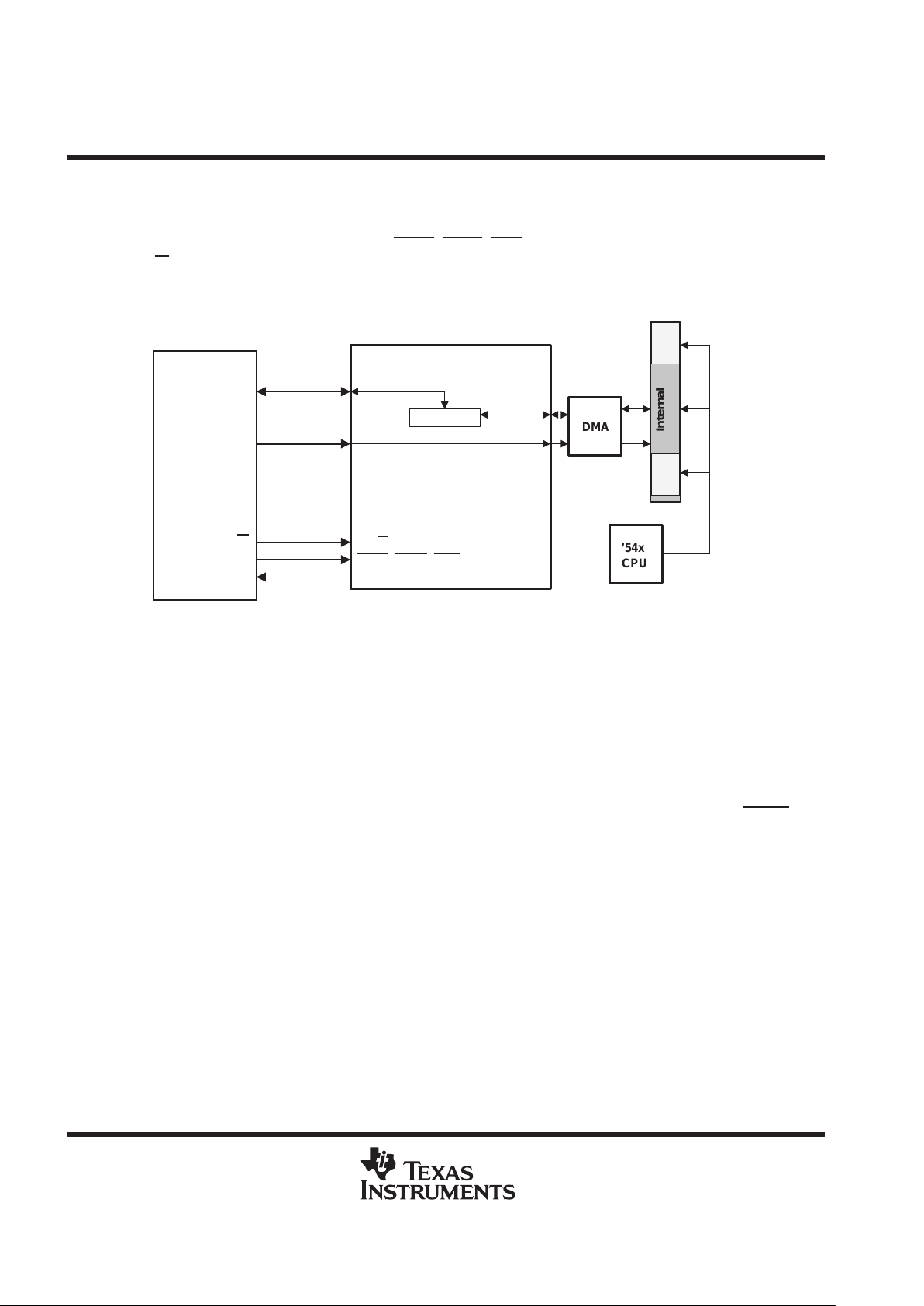
read or write access. Figure 7 shows a block diagram of the HPI16 in
nonmultiplexed
mode.
HOST
HPI-16
Data[15:0]
HD[15:0]
R/W
HR/W
Data strobes
HDS1, HDS2, HCS
HRDY
Ready
HPID[15:0]
DMA
’54x
CPU
Internal
memory
Address[n:0]
HA[n:0]
Figure 7. Interfacing to the HPI-16 in Non-Multiplexed Mode
other HPI16 system considerations
operation during IDLE
The HPI16 can continue to operate during IDLE1 or IDLE2 by using special clock management logic that turns
on relevant clocks to perform a synchronous memory access, and then turns the clocks back off to save power .
The DSP CPU does not wake up from the IDLE mode during this process.
downloading code during reset
The HPI16 can download code while the DSP is in reset. However, the system provides a pin (HPIRS) that
provides a way to take the HPI16 module out of reset while leaving the DSP in reset. The maximum HPI16 data
rate is 33 MBps assuming no other DMA activity (100-MIPS DSP subsystem).
emulation considerations
The HPI16 can continue operation even when the DSP CPU is halted due to debugger breakpoints or other
emulation events.
ADVANCE
INFORMATION

TMS320VC5421
DIGITAL SIGNAL PROCESSOR
SPRS098 – DECEMBER 1999
27
POST OFFICE BOX 1443 • HOUSTON, TEXAS 77251–1443
multichannel buffered serial port (McBSP)
The ’5421 device provides high-speed, full-duplex serial ports that allow direct interface to other ’C54x/’LC54x
devices, codecs, and other devices in a system. There are six multichannel buffered serial ports (McBSPs) on
board (three per subsystem).
The McBSP provides:
Full-duplex communication
Double-buffer data registers, which allow a continuous data stream
Independent framing and clocking for receive and transmit
In addition, the McBSP has the following capabilities:
Direct interface to:
– T1/E1 framers
– MVIP switching-compatible and ST-BUS compliant devices
– IOM-2 compliant device
– AC97-compliant device
– Serial port interface (SPI)
Multichannel transmit and receive of up to 128 channels
A wide selection of data sizes, including: 8, 12, 16, 20, 24, or 32 bits
µ-law and A-law companding
Programmable polarity for both frame synchronization and data clocks
Programmable internal clock and frame generation
The ’5421 McBSPs have been enhanced to provide more flexibility in the choice of the sample rate generator
input clock source. On previous C5000 devices, the McBSP sample rate input clock can be driven from one of
two possible choices: the internal CPU clock , or the external CLKS pin. However, most C5000 devices have
only the internal CPU clock as a possible source because the CLKS pin is not implemented on most device
packages.
To accomodate applications that require an external reference clock for the sample rate generator, the ’5421
McBSPs allow either the receive clock pin (BCLKR) or the transmit clock pin (BCLKX) to be configured as the
input clock to the sample rate generator. This enhancement is enabled through two register bits: pin control
register (PCR) bit 7 – enhanced sample clock mode (SCLKME), and sample rate generator register 2 (SRGR2)
bit 13 – McBSP sample rate generator clock mode (CLKSM). SCLKME is an addition to the PCR contained in
the McBSPs on previous C5000 devices. The new bit layout of the PCR is shown in Figure 8. For a description
of the remaining bits, see
TMS320C54x DSP Reference Set, Volume 5: Enhanced Peripherals
(literature
number SPRU302).
15 14 13 12 11 10 9 8
Reserved XIOEN RIOEN FSXM FSRM CLKXM CLKRM
R,+0 RW,+0 RW,+0 RW,+0 RW,+0 RW,+0 RW,+0
765 432 1 0
SCLKME
CLKS_STAT DX_ST AT DR_STAT FSXP FSRP CLKXP CLKRP
RW,+0 R,+0 R,+0 R,+0 RW,+0 RW,+0 RW,+0 RW,+0
Note: R = Read, W = Write, +0 = Value at reset
Figure 8. Pin Control Register (PCR)
ADVANCE
INFORMATION
SPI is a trademark of Motorola Incorporated.
 Loading...