

Texas Instruments TLV5627IPWR, TLV5627IPW, TLV5627IDR, TLV5627ID, TLV5627CPWR Datasheet
...
TLV5627C, TLV5627I
2.7-V TO 5.5-V 8-BIT 4-CHANNEL DIGITAL-TO-ANALOG CONVERTERS
WITH POWER DOWN
SLAS232 – JUNE1999
1
POST OFFICE BOX 655303 • DALLAS, TEXAS 75265
D
Four 8-Bit D/A Converters
D
Programmable Settling Time
of 3 µs or 9 µs Typ
D
TMS320, (Q)SPI, and Microwire Compatible
Serial Interface
D
Low Power Consumption:
7 mW, Slow Mode – 5-V Supply
3 mW, Slow Mode – 3-V Supply
D
Reference Input Buffers
D
Monotonic Over Temperature
D
Dual 2.7-V to 5.5-V Supply (Separate Digital
and Analog Supplies)
D
Hardware Power Down
D
Software Power Down
D
Simultaneous Update
applications
D
Battery Powered Test Instruments
D
Digital Offset and Gain Adjustment
D
Industrial Process Controls
D
Machine and Motion Control Devices
D
Arbitrary Waveform Generation
description
The TLV5627 is a four channel, 8-bit voltage
output digital-to-analog converter (DAC) with a
flexible 4-wire serial interface. The 4-wire serial
interface allows glueless interface to TMS320,
SPI, QSPI, and Microwire serial ports. The
TL V5627 is programmed with a 16-bit serial word
comprised of a DAC address, individual DAC
control bits, and an 8-bit DAC value.
The device has provision for two supplies: one
digital supply for the serial interface (via pins
DV
DD
and DGND), and one for the DACs,
reference buffers and output buffers (via pins AV
DD
and AGND). Each supply is independent of the other, and
can be any value between 2.7 V and 5.5 V . The dual supplies allow a typical application where the DAC will be
controlled via a microprocessor operating on a 3-V supply (also used on pins DV
DD
and DGND), with the DACs
operating on a 5-V supply. The digital and analog supplies can be tied together.
The resistor string output voltage is buffered by an x2 gain rail-to-rail output buffer. The buffer features a
Class AB output stage to improve stability and reduce settling time. A rail-to-rail output stage and a power-down
mode make it ideal for single voltage, battery based applications. The settling time of the DAC is programmable
to allow the designer to optimize speed versus power dissipation. The settling time is chosen by the control bits
within the 16-bit serial input string. A high-impedance buffer is integrated on the REFINAB and REFINCD
terminals to reduce the need for a low source impedance drive to the terminal. REFINAB and REFINCD allow
DACs A and B to have a different reference voltage than DACs C and D.
The device, implemented with a CMOS process, is available in 16-terminal SOIC and TSSOP packages. The
TL V5627C is characterized for operation from 0 °C to 70°C. The TLV5627I is characterized for operation from
–40°C to 85°C.
Copyright 1999, Texas Instruments Incorporated
PRODUCTION DATA information is current as of publication date.
Products conform to specifications per the terms of Texas Instruments
standard warranty. Production processing does not necessarily include
testing of all parameters.
Please be aware that an important notice concerning availability, standard warranty, and use in critical applications of
Texas Instruments semiconductor products and disclaimers thereto appears at the end of this data sheet.
1
2
3
4
5
6
7
8
16
15
14
13
12
11
10
9
DV
DD
PD
LDAC
DIN
SCLK
CS
FS
DGND
AV
DD
REFINAB
OUTA
OUTB
OUTC
OUTD
REFINCD
AGND
(TOP VIEW)
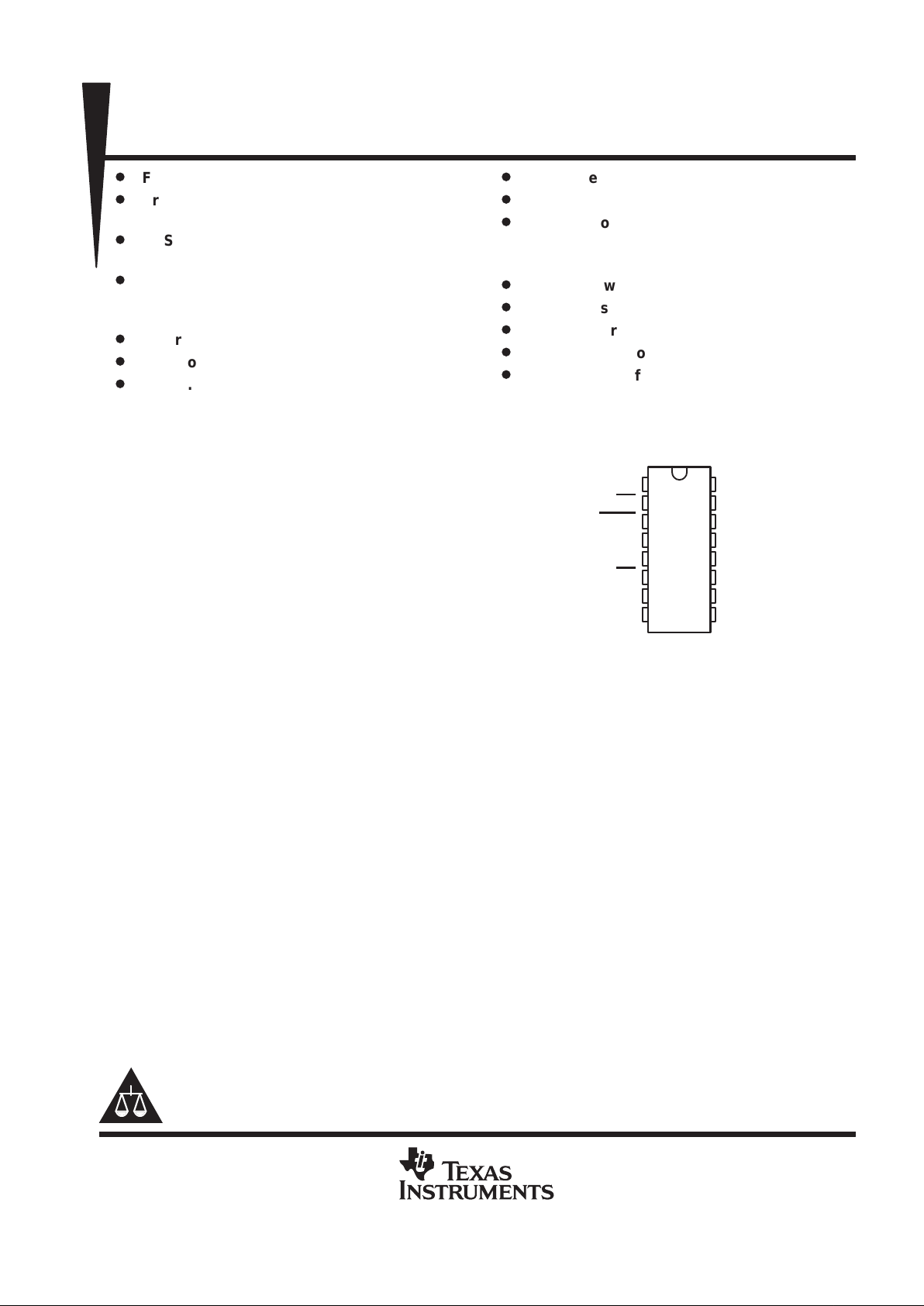
D OR PW PACKAGE
TLV5627C, TLV5627I
2.7-V TO 5.5-V 8-BIT 4-CHANNEL DIGITAL-TO-ANALOG CONVERTERS
WITH POWER DOWN
SLAS232 – JUNE1999
2
POST OFFICE BOX 655303 • DALLAS, TEXAS 75265
AVAILABLE OPTIONS
PACKAGE
T
A
SOIC
(D)
TSSOP
(PW)
0°C to 70°C TLV5627CD TLV5627CPW
–40°C to 85°C TLV5627ID TLV5627IPW
functional block diagram
7
5
Power-On
Reset
10-Bit
Data
and
Control
Register
REFINAB
AGND
CS
DIN
DAC A
Serial
Input
Register
6
9
8-Bit
DAC
Latch
2-Bit
Control
Data
Latch
Power Down/
Speed Control
_
+
8
2
2
8
10
OUTA
DAC
Select/
Control
Logic
FS
DAC B
DAC C
DAC D
OUTB
OUTC
OUTD
LDAC
PD
DGND
AV
DD
DV
DD
4
15 16 1
8
32
11
12
13
14
REFINCD
SCLK
2
x2
TLV5627C, TLV5627I
2.7-V TO 5.5-V 8-BIT 4-CHANNEL DIGITAL-TO-ANALOG CONVERTERS
WITH POWER DOWN
SLAS232 – JUNE1999
3
POST OFFICE BOX 655303 • DALLAS, TEXAS 75265
Terminal Functions
TERMINAL
NAME NO.
I/O
DESCRIPTION
AGND 9 Analog ground
AV
DD
16 Analog supply
CS 6 I Chip select. This terminal is active low.
DGND 8 Digital ground
DIN 4 I Serial data input
DV
DD
1 Digital supply
FS 7 I Frame sync input. The falling edge of the frame sync pulse indicates the start of a serial data frame shifted out
to the TLV5627.
PD 2 I Power-down pin. Powers down all DACs (overriding their individual power down settings), and all output stages.
This terminal is active low.
LDAC 3 I Load DAC. When the LDAC signal is high, no DAC output updates occur when the input digital data is read into
the serial interface. The DAC outputs are only updated when LDAC
is low.
REFINAB 15 I Voltage reference input for DACs A and B.
REFINCD 10 I Voltage reference input for DACs C and D.
SCLK 5 I Serial clock input
OUTA 14 O DAC A output
OUTB 13 O DAC B output
OUTC 12 O DAC C output
OUTD 11 O DAC D output
absolute maximum ratings over operating free-air temperature range (unless otherwise noted)
†
Supply voltage, (DV
DD
, AVDD to GND) 7 V. . . . . . . . . . . . . . . . . . . . . . . . . . . . . . . . . . . . . . . . . . . . . . . . . . . . . . . .
Supply voltage difference, (AV
DD
to DVDD) –2.8 V to 2.8 V. . . . . . . . . . . . . . . . . . . . . . . . . . . . . . . . . . . . . . . . . .
Digital input voltage range –0.3 V to DV
DD
+ 0.3 V. . . . . . . . . . . . . . . . . . . . . . . . . . . . . . . . . . . . . . . . . . . . . . . . .
Reference input voltage range –0.3 V to AV
DD
+ 0.3 V. . . . . . . . . . . . . . . . . . . . . . . . . . . . . . . . . . . . . . . . . . . . . .
Operating free-air temperature range, T
A
: TLV5627C 0°C to 70°C. . . . . . . . . . . . . . . . . . . . . . . . . . . . . . . . . . .
TLV5627I –40°C to 85°C. . . . . . . . . . . . . . . . . . . . . . . . . . . . . . . . . .
Storage temperature range, T
stg
–65°C to 150° C. . . . . . . . . . . . . . . . . . . . . . . . . . . . . . . . . . . . . . . . . . . . . . . . . . .
Lead temperature 1,6 mm (1/16 inch) from case for 10 seconds 260°C. . . . . . . . . . . . . . . . . . . . . . . . . . . . . . .
†
Stresses beyond those listed under “absolute maximum ratings” may cause permanent damage to the device. These are stress ratings only, and
functional operation of the device at these or any other conditions beyond those indicated under “recommended operating conditions” is not
implied. Exposure to absolute-maximum-rated conditions for extended periods may affect device reliability.
TLV5627C, TLV5627I
2.7-V TO 5.5-V 8-BIT 4-CHANNEL DIGITAL-TO-ANALOG CONVERTERS
WITH POWER DOWN
SLAS232 – JUNE1999
4
POST OFFICE BOX 655303 • DALLAS, TEXAS 75265
recommended operating conditions
MIN NOM MAX UNIT
pp
5-V supply 4.5 5 5.5
Suppl
y v
oltage, AV
DD
,
DV
DD
3-V supply 2.7 3 3.3
V
High-level digital input, V
IH
DVDD = 2.7 V to 5.5 V 2 V
Low-level digital input, V
IL
DVDD = 2.7 V to 5.5 V 0.8 V
5-V supply (see Note 1) 0 2.048 AVDD–1.5
Reference voltage, V
ref
to REFINAB, REFINCD terminal
3-V supply (see Note 1) 0 1.024 AVDD–1.5
V
Load resistance, R
L
2 10 kΩ
Load capacitance, C
L
100 pF
Serial clock rate, SCLK 20 MHz
p
p
TLV5627C 0 70
°
Operating free-air temperature
TLV5627I –40 85
°C
NOTE 1: Voltages greater than AVDD/2 will cause output saturation for large DAC codes.
electrical characteristics over recommended operating free-air temperature range
(unless otherwise noted)
static DAC specifications
PARAMETER TEST CONDITIONS MIN TYP MAX UNIT
Resolution 8 bits
Integral nonlinearity (INL), end point adjusted See Note 2 ±0.3 ±0.5 LSB
Differential nonlinearity (DNL) See Note 3 ±0.03 ±0.5 LSB
E
ZS
Zero scale error (offset error at zero scale) See Note 4 ±10 mV
Zero scale error temperature coefficient See Note 5 10 ppm/°C
E
G
Gain error See Note 6 ±0.6
%of FS
voltage
Gain error temperature coefficient See Note 7 10 ppm/°C
NOTES: 2. The relative accuracy or integral nonlinearity (INL) sometimes referred to as linearity error , is the maximum deviation of the output
from the line between zero and full scale excluding the effects of zero code and full-scale errors.
3. The differential nonlinearity (DNL) sometimes referred to as differential error, is the difference between the measured and ideal
1 LSB amplitude change of any two adjacent codes. Monotonic means the output voltage changes in the same direction (or remains
constant) as a change in the digital input code.
4. Zero-scale error is the deviation from zero voltage output when the digital input code is zero.
5. Zero-scale-error temperature coefficient is given by: EZS TC = [EZS (T
max
) – EZS (T
min
)]/V
ref
× 106/(T
max
– T
min
).
6. Gain error is the deviation from the ideal output (2V
ref
– 1 LSB) with an output load of 10 kΩ excluding the effects of the zero-error.
7. Gain temperature coef ficient is given by: EG TC = [EG(T
max
) – EG (T
min
)]/V
ref
× 106/(T
max
– T
min
).
TLV5627C, TLV5627I
2.7-V TO 5.5-V 8-BIT 4-CHANNEL DIGITAL-TO-ANALOG CONVERTERS
WITH POWER DOWN
SLAS232 – JUNE1999
5
POST OFFICE BOX 655303 • DALLAS, TEXAS 75265
electrical characteristics over recommended operating free-air temperature range
(unless otherwise noted) (continued)
individual DAC output specifications
PARAMETER TEST CONDITIONS MIN TYP MAX UNIT
V
O
Voltage output RL = 10 kΩ 0 AVDD–0.1 V
Output load regulation accuracy RL = 2 kΩ vs 10 kΩ 0.1 0.25
% of FS
voltage
reference input (REFINAB, REFINCD)
PARAMETER TEST CONDITIONS MIN TYP MAX UNIT
V
I
Input voltage range See Note 8 0 AVDD–1.5 V
R
I
Input resistance 10 MΩ
C
I
Input capacitance 5 pF
Reference feed through
REFIN = 1 Vpp at 1 kHz + 1.024 V dc
(see Note 9)
–75 dB
p
Slow 0.5
Reference input bandwidth
REFIN
= 0.2
V
pp
+ 1.
024 V dc
Fast 1
MH
z
NOTES: 8. Reference input voltages greater than VDD/2 will cause output saturation for large DAC codes.
9. Reference feedthrough is measured at the DAC output with an input code = 000 hex and a V
ref(REFINAB or REFINCD)
input = 1.024 Vdc + 1 Vpp at 1 kHz.
digital inputs (D0–D11, CS, WEB, LDAC, PD)
PARAMETER TEST CONDITIONS MIN TYP MAX UNIT
I
IH
High-level digital input current VI = DV
DD
±1 µA
I
IL
Low-level digital input current VI = 0 V ±1 µA
C
I
Input capacitance 3 pF
power supply
PARAMETER TEST CONDITIONS MIN TYP MAX UNIT
pp
Slow 1.4 2.2
pp
5-V suppl
y, No
load, Clock running
Fast 3.5 5.5
mA
IDDPower supply current
pp
Slow 1 1.5
3-V suppl
y, No
load, Clock running
Fast 3 4.5
mA
Power down supply current, See Figure 12 1 µA
pp
Zero scale gain
–68
PSRR
Power supply rejection ratio
Gain
See Notes 10 and 11
–68
dB
10. Zero-scale-error rejection ratio (EZS–RR) is measured by varying the AVDD from 5 ±0.5 V and 3 ±0.5 V dc, and measuring the
proportion of this signal imposed on the zero-code output voltage.
11. Gain-error rejection ratio (EG-RR) is measured by varying the A VDD from 5 ±0.5 V and 3 ±0.5 V dc and measuring the proportion
of this signal imposed on the full-scale output voltage after subtracting the zero scale change.
TLV5627C, TLV5627I
2.7-V TO 5.5-V 8-BIT 4-CHANNEL DIGITAL-TO-ANALOG CONVERTERS
WITH POWER DOWN
SLAS232 – JUNE1999
6
POST OFFICE BOX 655303 • DALLAS, TEXAS 75265
electrical characteristics over recommended operating free-air temperature range
(unless otherwise noted) (continued)
analog output dynamic performance
PARAMETER TEST CONDITIONS MIN TYP MAX UNIT
p
CL = 100 pF, RL = 10 kΩ,
Fast 5 V/µs
SR
Output slew rate
V
O
=
10% to 90%
,
V
ref
= 2.048 V , 1024 V
Slow 1 V/µs
p
To ± 0.1 LSB, C
= 100 pF,
Fast 2.5 4
tsOutput settling time
,
L
,
RL = 10 kΩ, See Notes 12 and 14
Slow 8.5 18
µ
s
p
To ± 0.1 LSB, C
= 100 pF,
Fast 1
t
s(c)
Output settling time, code to code
,
L
,
RL = 10 kΩ, See Notes 13 and 14
Slow 2
µ
s
Glitch energy Code transition from 7F0 to 800 10 nV-sec
SNR Signal-to-noise ratio
57
S/(N+D) Signal to noise + distortion
Sinewave generated by DAC
,
Reference volta
g
e = 1.024 at 3 V and 2.048 at 5 V ,
49
THD Total harmonic distortion
g,
fs = 400 KSPS, f
OUT
= 1.1 kHz sinewave,
–50
dB
SFDR Spurious free dynamic range
C
L
=
100 pF
,
R
L
= 10 kΩ, BW = 20 kHz
60
NOTES: 12. Settling time is the time for the output signal to remain within ± 0.1 LSB of the final measured value for a digital input code change
of 0x020 to 0xFF0 or 0xFF0 to 0x020.
13. Settling time is the time for the output signal to remain within ± 0.1 LSB of the final measured value for a digital input code change
of one count.
14. Limits are ensured by design and characterization, but are not production tested.
digital input timing requirements
MIN NOM MAX UNIT
t
su(CS–FS)
Setup time, CS low before FS↓ 10 ns
t
su(FS–CK)
Setup time, FS low before first negative SCLK edge 8 ns
t
su(C16–FS)
Setup time, sixteenth negative edge after FS low on which bit D0 is sampled before rising
edge of FS
10 ns
t
su(C16–CS)
Setup time, sixteenth positive SCLK edge (first positive after D0 is sampled) before CS rising
edge. If FS is used instead of the sixteenth positive edge to update the DAC, then the setup
time is between the FS rising edge and CS
rising edge.
10 ns
t
wH
Pulse duration, SCLK high 25 ns
t
wL
Pulse duration, SCLK low 25 ns
t
su(D)
Setup time, data ready before SCLK falling edge 8 ns
t
h(D)
Hold time, data held valid after SCLK falling edge 5 ns
t
wH(FS)
Pulse duration, FS high 20 ns

TLV5627C, TLV5627I
2.7-V TO 5.5-V 8-BIT 4-CHANNEL DIGITAL-TO-ANALOG CONVERTERS
WITH POWER DOWN
SLAS232 – JUNE1999
7
POST OFFICE BOX 655303 • DALLAS, TEXAS 75265
PARAMETER MEASUREMENT INFORMATION
ÎÎÎ
123451516
D15 D14 D13 D12 D1 D0
t
su(FS-CK)
t
su(CS-FS)
t
wH(FS)
t
h(D)
t
su(D)
t
wH
t
wL
t
su(C16-CS)
t
su(C16-FS)
SCLK
DIN
CS
FS
Figure 1. Timing Diagram
TLV5627C, TLV5627I
2.7-V TO 5.5-V 8-BIT 4-CHANNEL DIGITAL-TO-ANALOG CONVERTERS
WITH POWER DOWN
SLAS232 – JUNE1999
8
POST OFFICE BOX 655303 • DALLAS, TEXAS 75265
TYPICAL CHARACTERISTICS
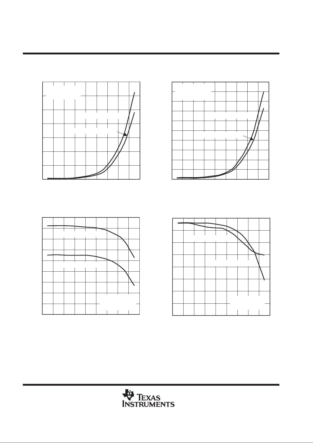
Figure 2
0.20
0.10
0.05
0
0 0.02 0.04 0.1 0.2 0.4 1
– Output Voltage – V
0.25
0.30
Load Current – mA
LOAD REGULATION
0.35
24
0.15
V
O
VDD = 5 V,
V
REF
= 2 V,
VO = Full Scale
5 V Slow Mode, Sink
5 V Fast Mode, Sink
Figure 3
0.10
0.08
0.04
0
0 0.01 0.02 0.05 0.1 0.2 0.5
0.16
0.18
LOAD REGULATION
0.20
12
0.14
0.12
0.06
0.02
– Output Voltage – V
Load Current – mA
V
O
VDD = 3 V,
V
REF
= 1 V,
VO = Full Scale
3 V Slow Mode, Sink
3 V Fast Mode, Sink
Figure 4
3.994
3.99
3.986
3.984
0 0.02 0.04 0.1 0.2 0.4 1
3.996
4.00
LOAD REGULATION
4.002
24
3.998
3.992
3.988
– Output Voltage – V
Load Current – mA
V
O
VDD = 5 V,
V
REF
= 2 V,
VO = Full Scale
5 V Slow Mode, Source
5 V Fast Mode, Source
Figure 5
2.001
2
1.999
1.999
0 0.01 0.02 0.05 0.1 0.2 0.5
2.002
2.002
LOAD REGULATION
2.003
12
2.001
2
– Output Voltage – V
Load Current – mA
V
O
VDD = 3 V,
V
REF
= 1 V,
VO = Full Scale
3 V Slow Mode, Source
3 V Fast Mode, Source

TLV5627C, TLV5627I
2.7-V TO 5.5-V 8-BIT 4-CHANNEL DIGITAL-TO-ANALOG CONVERTERS
WITH POWER DOWN
SLAS232 – JUNE1999
9
POST OFFICE BOX 655303 • DALLAS, TEXAS 75265
TYPICAL CHARACTERISTICS
Figure 6
2.5
2
1.5
0.5
–55 –40 –25 0 25 40 70
– Supply Current – mA
3
3.5
SUPPLY CURRENT
vs
TEMPERATURE
4
85 125
1
T – Temperature – ° C
I
DD
Fast Mode
Slow Mode
VDD = 3 V,
V
REF
= 1.024 V ,
VO = Full Scale
Figure 7
2.5
2
1.5
0.5
–55 –40 –25 0 25 40 70
– Supply Current – mA
3
3.5
SUPPLY CURRENT
vs
TEMPERATURE
4
85 125
1
T – Temperature – ° C
I
DD
Fast Mode
Slow Mode
VDD = 5 V,
V
REF
= 1.024 V ,
VO = Full Scale
Figure 8
––40
–50
–70
–80
0 5 10 20
THD – Total Harmonic Distortion – dB
–30
–10
f – Frequency – kHz
TOTAL HARMONIC DISTORTION
vs
FREQUENCY
0
30 50 100
–20
–60
V
ref
= 1 V dc + 1 V p/p Sinewave,
Output Full Scale
Fast Mode
Figure 9
––40
–50
–70
–80
0 5 10 20
THD – Total Harmonic Distortion – dB
–30
–10
f – Frequency – kHz
TOTAL HARMONIC DISTORTION
vs
FREQUENCY
0
30 50 100
–20
–60
V
ref
= 1 V dc + 1 V p/p Sinewave,
Output Full Scale
Slow Mode
TLV5627C, TLV5627I
2.7-V TO 5.5-V 8-BIT 4-CHANNEL DIGITAL-TO-ANALOG CONVERTERS
WITH POWER DOWN
SLAS232 – JUNE1999
10
POST OFFICE BOX 655303 • DALLAS, TEXAS 75265
TYPICAL CHARACTERISTICS
Figure 10
––40
–50
–70
–80
0 5 10 20
THD – Total Harmonic Distortion And Noise – dB
–30
–10
f – Frequency – kHz
TOTAL HARMONIC DISTORTION AND NOISE
vs
FREQUENCY
0
30 50 100
–20
–60
V
ref
= 1 V dc + 1 V p/p Sinewave,
Output Full Scale
Fast Mode
Figure 11
––40
–50
–70
–80
0 5 10 20
–30
–10
f – Frequency – kHz
TOTAL HARMONIC DISTORTION AND NOISE
vs
FREQUENCY
0
30 50 100
–20
–60
V
ref
= 1 V dc + 1 V p/p Sinewave,
Output Full Scale
THD – Total Harmonic Distortion And Noise – dB
Slow Mode
2000
1500
1000
0
0 200 400 600
– Supply Current –
3000
3500
t – Time – ns
SUPPLY CURRENT
vs
TIME
(WHEN ENTERING POWER-DOWN MODE)
4000
800 1000
2500
500
I
DD
Aµ
Figure 12

TLV5627C, TLV5627I
2.7-V TO 5.5-V 8-BIT 4-CHANNEL DIGITAL-TO-ANALOG CONVERTERS
WITH POWER DOWN
SLAS232 – JUNE1999
11
POST OFFICE BOX 655303 • DALLAS, TEXAS 75265
TYPICAL CHARACTERISTICS
Figure 13
–0.20
–0.15
–0.10
–0.05
–0.00
0.05
0.10
0.15
0.20
0 255
DNL – Differential Nonlinearity – LSB
Digital Output Code
DIFFERENTIAL NONLINEARITY
vs
DIGITAL OUTPUT CODE
12864 192
Figure 14
–0.40
–0.30
–0.20
–0.10
–0.00
0.10
0.20
0.30
0.40
0 255
INL – Integral Nonlinearity – LSB
Digital Output Code
INTEGRAL NONLINEARITY
vs
DIGITAL OUTPUT CODE
64 128 192
TLV5627C, TLV5627I
2.7-V TO 5.5-V 8-BIT 4-CHANNEL DIGITAL-TO-ANALOG CONVERTERS
WITH POWER DOWN
SLAS232 – JUNE1999
12
POST OFFICE BOX 655303 • DALLAS, TEXAS 75265
APPLICATION INFORMATION
general function
The TL V5627 is an 8-bit single supply DAC based on a resistor string architecture. The device consists of a serial
interface, speed and power-down control logic, a reference input buffer , a resistor string, and a rail-to-rail output
buffer .
The output voltage (full scale determined by external reference) is given by:
2REF
CODE
0x1000
[V]
Where REF is the reference voltage and CODE is the digital input value within the range of 0x000 to 0xFF0.
Bits 3 to 0 must be set to zero. A power-on reset initially resets the internal latches to a defined state (all bits
zero).
serial interface
The device has to be enabled with CS set to low. A falling edge of FS starts shifting the data bit-per-bit (starting
with the MSB) to the internal register on the falling edges of SCLK. After 16 bits have been transferred or FS
rises, the content of the shift register is moved to the DAC latch, which updates the voltage output to the new
level.
The serial interface of the TLV5627 can be used in two basic modes:
D
Four wire (with chip select)
D
Three wire (without chip select)
Using chip select (four-wire mode), it is possible to have more than one device connected to the serial port of
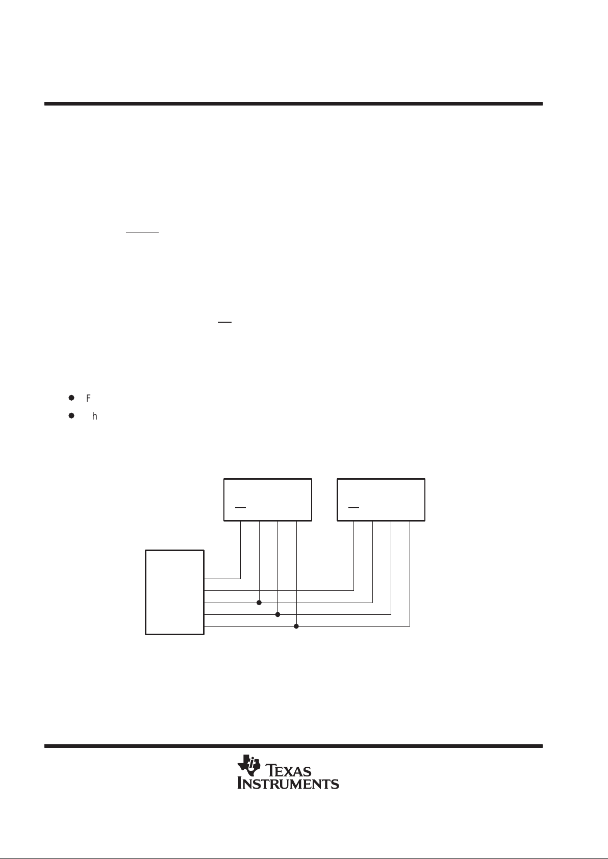
the data source (DSP or microcontroller). The interface is compatible with the TMS320 family . Figure 15 shows
an example with two TLV5627s connected directly to a TMS320 DSP.
TMS320
DSP
XF0
XF1
FSX
DX
CLKX
TLV5627
CS
FS DIN SCLK
TLV5627
CS
FS DIN SCLK
Figure 15. TMS320 Interface
TLV5627C, TLV5627I
2.7-V TO 5.5-V 8-BIT 4-CHANNEL DIGITAL-TO-ANALOG CONVERTERS
WITH POWER DOWN
SLAS232 – JUNE1999
13
POST OFFICE BOX 655303 • DALLAS, TEXAS 75265
APPLICATION INFORMATION
serial interface (continued)
If there is no need to have more than one device on the serial bus, then CS can be tied low. Figure 16 shows
an example of how to connect the TLV5627 to a TMS320, SPI, or Microwire port using only three pins.
TMS320
DSP
FSX
DX
CLKX
TLV5627
FS
DIN
SCLK
CS
SPI
SS
MOSI
SCLK
TLV5627
FS
DIN
SCLK
CS
Microwire
I/O
SO
SK
TLV5627
FS
DIN
SCLK
CS
Figure 16. Three-Wire Interface
Notes on SPI and Microwire: Before the controller starts the data transfer, the software has to generate a falling
edge on the I/O pin connected to FS. If the word width is 8 bits (SPI and Microwire), two write operations must
be performed to program the TLV5627. After the write operation(s), the DAC output is updated automatically
on the sixteenth positive clock edge.
serial clock frequency and update rate
The maximum serial clock frequency is given by:
f
SCLKmax
+
1
t
wH(min)
)
t
wL(min)
+
20 MHz
The maximum update rate is:
f
UPDATEmax
+
1
16
ǒ
t
wH(min)
)
t
wL(min)
Ǔ
+
1.25 MHz
The maximum update rate is a theoretical value for the serial interface since the settling time of the TL V5627
has to be considered also.
data format
The 16-bit data word for the TLV5627 consists of two parts:
D
Control bits (D15 . . . D12)
D
New DAC value (D11 ...D0)
D15 D14 D13 D12 D11 D10 D9 D8 D7 D6 D5 D4 D3 D2 D1 D0
A1 A0 PWR SPD New DAC value (8 bits) 0 0 0 0
SPD: Speed control bit. 1 → fast mode 0 → slow mode
PWR: Power control bit. 1 → power down 0 → normal operation

TLV5627C, TLV5627I
2.7-V TO 5.5-V 8-BIT 4-CHANNEL DIGITAL-TO-ANALOG CONVERTERS
WITH POWER DOWN
SLAS232 – JUNE1999
14
POST OFFICE BOX 655303 • DALLAS, TEXAS 75265
APPLICATION INFORMATION
In power-down mode, all amplifiers within the TLV5627 are disabled. A particular DAC (A, B, C, D) of the
TLV5627 is selected by A1 and A0 within the input word.
A1 A0 DAC
0 0 A
0 1 B
1 0 C
1 1 D
TLV5627 interfaced to TMS320C203 DSP
hardware interfacing
Figure 17 shows an example of how to connect the TLV5627 to a TMS320C203 DSP. The serial port is
configured in burst mode, with FSX generated by the TMS320C203 to provide the frame sync (FS) input to the
TL V5627. Data is transmitted on the DX line, with the serial clock input on the CLKX line. The general-purpose
input/output port bits IO0 and IO1 are used to generate the chip select (CS
) and DAC latch update (LDAC)
inputs to the TLV5627. The active low power down ( PD
) is pulled high all the time to ensure the DACs are
enabled.
DX
CLKX
FSX
I/O 0
I/O 1
TMS320C203
SDIN
SCLK
FS
CS
LDAC
REF
V
DD
PD
VOUTA
VOUTB
VOUTC
VOUTD
V
SS
TLV5627
REFINAB
REFINCD
Figure 17. TLV5627 Interfaced with TMS320C203

TLV5627C, TLV5627I
2.7-V TO 5.5-V 8-BIT 4-CHANNEL DIGITAL-TO-ANALOG CONVERTERS
WITH POWER DOWN
SLAS232 – JUNE1999
15
POST OFFICE BOX 655303 • DALLAS, TEXAS 75265
APPLICATION INFORMATION
TLV5627 interfaced to MCS
51 microcontroller
hardware interfacing
Figure 18 shows an example of how to connect the TLV5627 to an MCS
51 Microcontroller. The serial DAC
input data and external control signals are sent via I/O Port 3 of the controller. The serial data is sent on the RxD
line, with the serial clock output on the TxD line. Port 3 bits 3, 4, and 5 are configured as outputs to provide the
DAC latch update (LDAC
), chip select (CS) and frame sync (FS) signals for the TL V5627. The active low power
down pin (PD
) of the TLV5627 is pulled high to ensure that the DACs are enabled.
RxD
TxD
P3.3
P3.4
MCS
®
51
SDIN
SCLK
FS
CS
LDAC
REF
V
DD
PD
VOUTA
VOUTB
VOUTC
VOUTD
V
SS
TLV5627
P3.4
REFINAB
REFINCD
Figure 18. TLV5627 Interfaced with MCS51
linearity, offset, and gain error using single ended supplies
When an amplifier is operated from a single supply , the voltage offset can still be either positive or negative. With
a positive offset, the output voltage changes on the first code change. With a negative offset, the output voltage
may not change with the first code, depending on the magnitude of the offset voltage.
The output amplifier attempts to drive the output to a negative voltage. However, because the most negative
supply rail is ground, the output cannot drive below ground and clamps the output at 0 V.
The output voltage then remains at zero until the input code value produces a sufficient positive output voltage
to overcome the negative offset voltage, resulting in the transfer function shown in Figure 19.
DAC Code
Output
Voltage
0 V
Negative
Offset
Figure 19. Effect of Negative Offset (single supply)
MCS is a registered trademark of Intel Corporation.

TLV5627C, TLV5627I
2.7-V TO 5.5-V 8-BIT 4-CHANNEL DIGITAL-TO-ANALOG CONVERTERS
WITH POWER DOWN
SLAS232 – JUNE1999
16
POST OFFICE BOX 655303 • DALLAS, TEXAS 75265
APPLICATION INFORMATION
linearity, offset, and gain error using single ended supplies (continued)
The offset error, not the linearity error, produces this breakpoint. The transfer function would have followed the
dotted line if the output buffer could drive below the ground rail.
For a DAC, linearity is measured between zero-input code (all inputs 0) and full-scale code (all inputs 1) after
offset and full scale are adjusted out or accounted for in some way . However , single supply operation does not
allow for adjustment when the offset is negative due to the breakpoint in the transfer function. So the linearity
is measured between full-scale code and the lowest code that produces a positive output voltage.
power-supply bypassing and ground management
Printed-circuit boards that use separate analog and digital ground planes offer the best system performance.
Wire-wrap boards do not perform well and should not be used. The two ground planes should be connected
together at the low-impedance power-supply source. The best ground connection may be achieved by
connecting the DAC AGND terminal to the system analog ground plane, making sure that analog ground
currents are well-managed and there are negligible voltage drops across the ground plane.
A 0.1-µF ceramic-capacitor bypass should be connected between V
DD
and AGND and mounted with short leads
as close as possible to the device. Use of ferrite beads may further isolate the system analog supply from the
digital power supply.
Figure 20 shows the ground plane layout and bypassing technique.
0.1 µF
Analog Ground Plane
1
2
3
4
8
7
6
5
Figure 20. Power-Supply Bypassing

TLV5627C, TLV5627I
2.7-V TO 5.5-V 8-BIT 4-CHANNEL DIGITAL-TO-ANALOG CONVERTERS
WITH POWER DOWN
SLAS232 – JUNE1999
17
POST OFFICE BOX 655303 • DALLAS, TEXAS 75265
MECHANICAL DATA
D (R-PDSO-G**) PLASTIC SMALL-OUTLINE PACKAGE
14 PIN SHOWN
4040047/D 10/96
0.228 (5,80)
0.244 (6,20)
0.069 (1,75) MAX
0.010 (0,25)
0.004 (0,10)
1
14
0.014 (0,35)
0.020 (0,51)
A
0.157 (4,00)
0.150 (3,81)
7
8
0.044 (1,12)
0.016 (0,40)
Seating Plane
0.010 (0,25)
PINS **
0.008 (0,20) NOM
A MIN
A MAX
DIM
Gage Plane
0.189
(4,80)
(5,00)
0.197
8
(8,55)
(8,75)
0.337
14
0.344
(9,80)
16
0.394
(10,00)
0.386
0.004 (0,10)
M
0.010 (0,25)
0.050 (1,27)
0°–8°
NOTES: A. All linear dimensions are in inches (millimeters).
B. This drawing is subject to change without notice.
C. Body dimensions do not include mold flash or protrusion, not to exceed 0.006 (0,15).
D. Falls within JEDEC MS-012

TLV5627C, TLV5627I
2.7-V TO 5.5-V 8-BIT 4-CHANNEL DIGITAL-TO-ANALOG CONVERTERS
WITH POWER DOWN
SLAS232 – JUNE1999
18
POST OFFICE BOX 655303 • DALLAS, TEXAS 75265
MECHANICAL DATA
PW (R-PDSO-G**) PLASTIC SMALL-OUTLINE PACKAGE
4040064/E 08/96
14 PIN SHOWN
Seating Plane
1,20 MAX
1
A
7
14
0,19
4,50
4,30
8
6,20
6,60
0,30
0,75
0,50
0,25
Gage Plane
0,15 NOM
0,65
M
0,10
0°–8°
0,10
PINS **
A MIN
A MAX
DIM
2,90
3,10
8
4,90
5,10
14
6,60
6,404,90
5,10
16
7,70
20
7,90
24
9,60
9,80
28
0,15
0,05
NOTES: A. All linear dimensions are in millimeters.
B. This drawing is subject to change without notice.
C. Body dimensions do not include mold flash or protrusion not to exceed 0,15.
D. Falls within JEDEC MO-153

IMPORTANT NOTICE
T exas Instruments and its subsidiaries (TI) reserve the right to make changes to their products or to discontinue
any product or service without notice, and advise customers to obtain the latest version of relevant information
to verify, before placing orders, that information being relied on is current and complete. All products are sold
subject to the terms and conditions of sale supplied at the time of order acknowledgement, including those
pertaining to warranty, patent infringement, and limitation of liability.
TI warrants performance of its semiconductor products to the specifications applicable at the time of sale in
accordance with TI’s standard warranty. Testing and other quality control techniques are utilized to the extent
TI deems necessary to support this warranty. Specific testing of all parameters of each device is not necessarily
performed, except those mandated by government requirements.
CERT AIN APPLICATIONS USING SEMICONDUCTOR PRODUCTS MAY INVOLVE POTENTIAL RISKS OF
DEATH, PERSONAL INJURY, OR SEVERE PROPERTY OR ENVIRONMENTAL DAMAGE (“CRITICAL
APPLICATIONS”). TI SEMICONDUCTOR PRODUCTS ARE NOT DESIGNED, AUTHORIZED, OR
WARRANTED TO BE SUITABLE FOR USE IN LIFE-SUPPORT DEVICES OR SYSTEMS OR OTHER
CRITICAL APPLICATIONS. INCLUSION OF TI PRODUCTS IN SUCH APPLICA TIONS IS UNDERST OOD TO
BE FULLY AT THE CUSTOMER’S RISK.
In order to minimize risks associated with the customer’s applications, adequate design and operating
safeguards must be provided by the customer to minimize inherent or procedural hazards.
TI assumes no liability for applications assistance or customer product design. TI does not warrant or represent
that any license, either express or implied, is granted under any patent right, copyright, mask work right, or other
intellectual property right of TI covering or relating to any combination, machine, or process in which such
semiconductor products or services might be or are used. TI’s publication of information regarding any third
party’s products or services does not constitute TI’s approval, warranty or endorsement thereof.
Copyright 1999, Texas Instruments Incorporated
 Loading...