

TLC3704, TLC3704Q
QUAD MICROPOWER LinCMOS VOLTAGE COMPARATORS
SLCS117A – NOVEMBER 1986 – REVISED OCT OBER 1996
1
POST OFFICE BOX 655303 • DALLAS, TEXAS 75265
D
Push-Pull CMOS Output Drives Capacitive
Loads Without Pullup Resistor,
I
O
= ± 8 mA
D
Very Low Power...200 µW Typ at 5 V
D
Fast Response Time ...t
PLH
= 2.7 µs Typ
With 5-mV Overdrive
D
Single Supply Operation...3 V to 16 V
TLC3704M ...4 V to 16 V
D
On-Chip ESD Protection
description
The TLC3704 consists of four independent
micropower voltage comparators designed to
operate from a single supply and be compatible
with modern HCMOS logic systems. They are
functionally similar to the LM339 but use 1/20th
the power for similar response times. The
push-pull CMOS output stage drives capacitive
loads directly without a power-consuming pullup
resistor to achieve the stated response time.
Eliminating the pullup resistor not only reduces
power dissipation, but also saves board space
and component cost. The output stage is also fully
compatible with TTL requirements.
Texas Instruments LinCMOS process offers
superior analog performance to standard CMOS
processes. Along with the standard CMOS
advantages of low power without sacrificing
speed, high input impedance, and low bias
currents, the LinCMOS process offers extremely
stable input offset voltages with large differential
input voltages. This characteristic makes it
possible to build reliable CMOS comparators.
The TLC3704C is characterized for operation over the commercial temperature range of 0°C to 70°C. The
TLC3704I is characterized for operation over the extended industrial temperature range of – 40°C to 85°C. The
TLC3704M is characterized for operation over the full military temperature range of – 55°C to 125°C. The
TLC3704Q is characterized for operation from – 40°C to 125°C.
Please be aware that an important notice concerning availability, standard warranty, and use in critical applications of
Texas Instruments semiconductor products and disclaimers thereto appears at the end of this data sheet.
LinCMOS is a trademark of Texas Instruments Incorporated.
Copyright 1996, Texas Instruments Incorporated
PRODUCTION DATA information is current as of publication date.
Products conform to specifications per the terms of Texas Instruments
standard warranty. Production processing does not necessarily include
testing of all parameters.
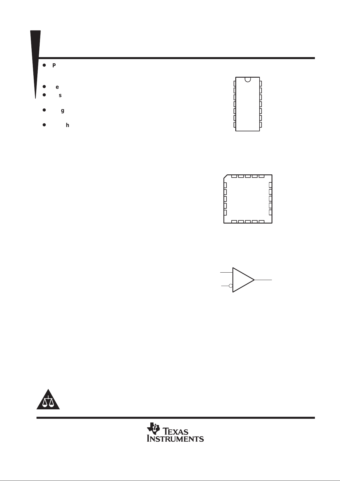
3 2 1 20 19
910111213
4
5
6
7
8
18
17
16
15
14
GND
NC
4IN+
NC
4IN–
V
DD
NC
2IN–
NC
2IN+
FK PACKAGE
(TOP VIEW)
2OUT
1OUT
NC
3IN–
3IN+
3OUT
4OUT
1IN+
NC
1IN–
D, J, OR N PACKAGE
(TOP VIEW)
NC – No internal connection
OUT
symbol (each comparator)
IN+
IN–
1
2
3
4
5
6
7
14
13
12
11
10
9
8
1OUT
2OUT
V
DD
2IN–
2IN+
1IN–
1IN+
3OUT
4OUT
GND
4IN+
4IN–
3IN+
3IN–
TLC3704, TLC3704Q
QUAD MICROPOWER LinCMOS VOLTAGE COMPARATORS
SLCS117A – NOVEMBER 1986 – REVISED OCT OBER 1996
2
POST OFFICE BOX 655303 • DALLAS, TEXAS 75265
AVAILABLE OPTIONS
PACKAGE
T
A
VIOmax
at 25°C
SMALL OUTLINE
(D)
CERAMIC
(FK)
CERAMIC DIP
(J)
PLASTIC DIP
(N)
0°C to 70°C 5 mV TLC3704CD — — TLC3704CN
–40°C to 85°C 5 mV TLC3704ID — — TLC3704IN
–55°C to 125°C 5 mV — TLC3704MFK TLC3704MJ —
–40°C to 125°C 5 mV — — TLC3704QJ —
The D package is available taped and reeled. Add R suffix to the device type (e.g., TLC3704CDR).
functional block diagram (each comparator)
V
DD
GND
OUT
Differential
Input
Circuits
IN+
IN–
absolute maximum ratings over operating free-air temperature range (unless otherwise noted)
†
Supply voltage range, V
DD
(see Note 1) – 0.3 V to 18 V. . . . . . . . . . . . . . . . . . . . . . . . . . . . . . . . . . . . . . . . . . . . .
Differential input voltage, V
ID
(see Note 2) ± 18 V. . . . . . . . . . . . . . . . . . . . . . . . . . . . . . . . . . . . . . . . . . . . . . . . . .
Input voltage range, V
I
– 0.3 to V
DD
. . . . . . . . . . . . . . . . . . . . . . . . . . . . . . . . . . . . . . . . . . . . . . . . . . . . . . . . . . . . . . .
Output voltage range, V
O
– 0.3 to V
DD
. . . . . . . . . . . . . . . . . . . . . . . . . . . . . . . . . . . . . . . . . . . . . . . . . . . . . . . . . . . .
Input current, I
I
± 5 mA. . . . . . . . . . . . . . . . . . . . . . . . . . . . . . . . . . . . . . . . . . . . . . . . . . . . . . . . . . . . . . . . . . . . . . . . . .
Output current, I
O
(each output) ± 20 mA. . . . . . . . . . . . . . . . . . . . . . . . . . . . . . . . . . . . . . . . . . . . . . . . . . . . . . . . . .
Total supply current into V
DD
40 mA. . . . . . . . . . . . . . . . . . . . . . . . . . . . . . . . . . . . . . . . . . . . . . . . . . . . . . . . . . . . . .
Total current out of GND 60 mA. . . . . . . . . . . . . . . . . . . . . . . . . . . . . . . . . . . . . . . . . . . . . . . . . . . . . . . . . . . . . . . . . .
Continuous total power dissipation See Dissipation Rating Table. . . . . . . . . . . . . . . . . . . . . . . . . . . . . . . . . . . . .
Operating free-air temperature range, T
A
: TLC3704C 0 to 70°C. . . . . . . . . . . . . . . . . . . . . . . . . . . . . . . . . . . . . . .
TLC3704I – 40°C to 85°C. . . . . . . . . . . . . . . . . . . . . . . . . . . . . . . . . . .
TLC3704M – 55°C to 125°C. . . . . . . . . . . . . . . . . . . . . . . . . . . . . . . .
TLC3704Q – 40°C to 125°C. . . . . . . . . . . . . . . . . . . . . . . . . . . . . . . .
Storage temperature range – 65°C to 150°C. . . . . . . . . . . . . . . . . . . . . . . . . . . . . . . . . . . . . . . . . . . . . . . . . . . . . . .
Case temperature for 60 seconds: FK package 260°C. . . . . . . . . . . . . . . . . . . . . . . . . . . . . . . . . . . . . . . . . . . . . .
Lead temperature 1,6 mm (1/16 inch) from case for 10 seconds: D or N package 260°C. . . . . . . . . . . . . . . .
Lead temperature 1,6 mm (1/16 inch) from case for 60 seconds: J package 300°C. . . . . . . . . . . . . . . . . . . . .
†
Stresses beyond those listed under “absolute maximum ratings” may cause permanent damage to the device. These are stress ratings only, and
functional operation of the device at these or any other conditions beyond those indicated under “recommended operating conditions” is not
implied. Exposure to absolute-maximum-rated conditions for extended periods may affect device reliability.
NOTES: 1. All voltage values, except differential voltages, are with respect to network ground.
2. Differential voltages are at IN+ with respect to IN–.
TLC3704, TLC3704Q
QUAD MICROPOWER LinCMOS VOLTAGE COMPARATORS
SLCS117A – NOVEMBER 1986 – REVISED OCT OBER 1996
3
POST OFFICE BOX 655303 • DALLAS, TEXAS 75265
DISSIPATION RATING TABLE
PACKAGE
TA ≤ 25°C
POWER RATING
DERATING FACTOR
ABOVE TA = 25°C
TA = 70°C
POWER RATING
TA = 85°C
POWER RATING
TA = 125°C
POWER RATING
D
FK
J
N
950 mW
1375 mW
1375 mW
1150 mW
7.6 mW/°C
11.0 mW/°C
11.0 mW/°C
9.2 mW/°C
608 mW
880 mW
880 mW
736 mW
494 mW
715 mW
715 mW
598 mW
N/A
275 mW
275 mW
N/A
recommended operating conditions
TLC3704C
MIN NOM MAX
UNIT
Supply voltage, V
DD
3 5 16 V
Common-mode input voltage, V
IC
– 0.2 VDD – 1.5 V
High-level output current, I
OH
– 20 mA
Low-level output current, I
OL
20 mA
Operating free-air temperature, T
A
0 70 °C
electrical characteristics at specified operating free-air temperature, VDD = 5 V
(unless otherwise noted)
TLC3704C
PARAMETER
TEST CONDITIONS
†
T
A
MIN TYP MAX
UNIT
p
VDD = 5 V to 10 V, 25°C 1.2 5
VIOInput offset voltage
VIC = V
ICR
min, See Note 3 0°C to 70°C 6.5
mV
p
25°C 1 pA
IIOInput offset current
V
IC
= 2.5
V
70°C 0.3 nA
p
25°C 5 pA
IIBInput bias current
V
IC
= 2.5
V
70°C 0.6 nA
p
25°C
0 to
VDD – 1
V
ICR
Common-mode input voltage range
0°C to 70°C
0 to
VDD – 1.5
V
25°C 84
CMRR Common-mode rejection ratio VIC = V
ICR
min
70°C 84
dB
0°C 84
25°C 85
k
SVR
Supply-voltage rejection ratio VDD = 5 V to 10 V
70°C 85
dB
0°C 85
p
25°C 4.5 4.7
VOHHigh-level output voltage
V
ID
= 1 V,
I
OH
= –4
mA
70°C 4.3
V
p
25°C 210 300
VOLLow-level output voltage
V
ID
= –1 V,
I
OH
= 4
mA
70°C 375
mV
pp
p
p
25°C 35 80
IDDSupply current (all four comparators)
Outputs lo
w,
No load
0°C to 70°C 100
µ
A
†
All characteristics are measured with zero common-mode voltage unless otherwise noted.
NOTE 3: The offset voltage limits given are the maximum values required to drive the output up to 4.5 V or down to 0.3 V.
TLC3704, TLC3704Q
QUAD MICROPOWER LinCMOS VOLTAGE COMPARATORS
SLCS117A – NOVEMBER 1986 – REVISED OCT OBER 1996
4
POST OFFICE BOX 655303 • DALLAS, TEXAS 75265
recommended operating conditions
TLC3704I
MIN NOM MAX
UNIT
Supply voltage, V
DD
3 5 16 V
Common-mode input voltage, V
IC
– 0.2 VDD – 1.5 V
High-level output current, I
OH
– 20 mA
Low-level output current, I
OL
20 mA
Operating free-air temperature, T
A
– 40 85 °C
electrical characteristics at specified operating free-air temperature, VDD = 5 V, VIC = 0 (unless
otherwise noted)
TLC3704I
PARAMETER
TEST CONDITIONS
T
A
MIN TYP MAX
UNIT
p
VDD = 5 V to 10 V, 25°C 1.2 5
VIOInput offset voltage
VIC = V
ICR
min, See Note 3 –40°C to 85°C 7
mV
p
25°C 1 pA
IIOInput offset current
V
IC
= 2.5
V
85°C 1 nA
p
25°C 5 pA
IIBInput bias current
V
IC
= 2.5
V
85°C 2 nA
p
25°C
0 to
VDD – 1
V
ICR
Common-mode input voltage range
–40°C to 85°C
0 to
VDD – 1.5
V
25°C 84
CMRR Common-mode rejection ratio VIC = V
ICR
min
85°C 84
dB
–40°C 83
25°C 85
k
SVR
Supply-voltage rejection ratio VDD = 5 V to 10 V
85°C 85
dB
–40°C 83
p
25°C 4.5 4.7
VOHHigh-level output voltage
V
ID
= 1 V,
I
OH
= –4
mA
85°C 4.3
V
p
25°C 210 300
VOLLow-level output voltage
V
ID
= –
1 V
,
I
OH
=
4 mA
85°C 400
mV
pp
p
p
25°C 35 80
IDDSupply current (all four comparators)
Outputs lo
w,
No load
–40°C to 85°C 125
µ
A
NOTE 3: The offset voltage limits given are the maximum values required to drive the output up to 4.5 V or down to 0.3 V.
TLC3704, TLC3704Q
QUAD MICROPOWER LinCMOS VOLTAGE COMPARATORS
SLCS117A – NOVEMBER 1986 – REVISED OCT OBER 1996
5
POST OFFICE BOX 655303 • DALLAS, TEXAS 75265
recommended operating conditions
TLC3704M
MIN NOM MAX
UNIT
Supply voltage, V
DD
4 5 16 V
Common-mode input voltage, V
IC
0 VDD – 1.5 V
High-level output current, I
OH
– 20 mA
Low-level output current, I
OL
20 mA
Operating free-air temperature, T
A
– 55 125 °C
electrical characteristics at specified operating free-air temperature, VDD = 5 V, VIC = 0 (unless
otherwise noted)
TLC3704M
PARAMETER
TEST CONDITIONS
T
A
MIN TYP MAX
UNIT
p
VDD = 5 V to 10 V, 25°C 1.2 5
VIOInput offset voltage
VIC = V
ICR
min, See Note 3 –55°C to 125°C 10
mV
p
25°C 1 pA
IIOInput offset current
V
IC
= 2.5
V
125°C 15 nA
p
25°C 5 pA
IIBInput bias current
V
IC
= 2.5
V
125°C 30 nA
p
25°C
0 to
VDD – 1
V
ICR
Common-mode input voltage range
–55°C to 125°C
0 to
VDD – 1.5
V
25°C 84
CMRR Common-mode rejection ratio VIC = V
ICR
min
125°C 83
dB
–55°C 82
25°C 85
k
SVR
Supply-voltage rejection ratio VDD = 5 V to 10 V
125°C 85
dB
–55°C 82
p
25°C 4.5 4.7
VOHHigh-level output voltage
V
ID
= 1 V,
I
OH
= –4
mA
125°C 4.2
V
p
25°C 210 300
VOLLow-level output voltage
V
ID
= –
1 V
,
I
OH
=
4 mA
125°C 500
mV
pp
p
p
25°C 35 80
IDDSupply current (all four comparators)
Outputs lo
w,
No load
–55°C to 125°C 175
µ
A
NOTE 3: The offset voltage limits given are the maximum values required to drive the output up to 4.5 V or down to 0.3 V.
TLC3704, TLC3704Q
QUAD MICROPOWER LinCMOS VOLTAGE COMPARATORS
SLCS117A – NOVEMBER 1986 – REVISED OCT OBER 1996
6
POST OFFICE BOX 655303 • DALLAS, TEXAS 75265
recommended operating conditions
TLC3704Q
MIN NOM MAX
UNIT
Supply voltage, V
DD
3 5 16 V
Common-mode input voltage, V
IC
–0.2 VDD – 1.5 V
High-level output current, I
OH
– 20 mA
Low-level output current, I
OL
20 mA
Operating free-air temperature, T
A
– 40 125 °C
electrical characteristics at specified operating free-air temperature, VDD = 5 V, VIC = 0 (unless
otherwise noted)
TLC3704Q
PARAMETER
TEST CONDITIONS
T
A
MIN TYP MAX
UNIT
p
VDD = 5 V to 10 V, 25°C 1.2 5
VIOInput offset voltage
VIC = V
ICR
min, See Note 3 –40°C to 125°C 7
mV
p
25°C 1 pA
IIOInput offset current
V
IC
= 2.5
V
125°C 15 nA
p
25°C 5 pA
IIBInput bias current
V
IC
= 2.5
V
125°C 30 nA
Common-mode input voltage
25°C 0 to VDD – 1
V
ICR
g
range
–40°C to 125°C 0 to VDD – 1.5
V
25°C 84
CMRR Common-mode rejection ratio VIC = V
ICR
min
125°C 83
dB
–40°C 83
25°C 85
k
SVR
Supply-voltage rejection ratio VDD = 5 V to 10 V
125°C 85
dB
–40°C 83
p
25°C 4.5 4.7
VOHHigh-level output voltage
V
ID
=
1 V
,
I
OH
= –
4 mA
125°C 4.2
V
p
25°C 210 300
VOLLow-level output voltage
V
ID
= –1 V,
I
OH
= 4
mA
125°C 500
mV
Supply current (all four
p
25°C 35 80
I
DD
y(
comparators)
Outputs lo
w,
No load
–40°C to 125°C 175
µ
A
NOTE 3: The offset voltage limits given are the maximum values required to drive the output up to 4.5 V or down to 0.3 V.
TLC3704, TLC3704Q
QUAD MICROPOWER LinCMOS VOLTAGE COMPARATORS
SLCS117A – NOVEMBER 1986 – REVISED OCT OBER 1996
7
POST OFFICE BOX 655303 • DALLAS, TEXAS 75265
switching characteristics, VDD = 5 V, TA = 25°C
PARAMETER TEST CONDITIONS
TLC3704C, TLC3704I
TLC3704M, TLC3704Q
UNIT
MIN TYP MAX
Overdrive = 2 mV 4.5
Overdrive = 5 mV 2.7
p
p
f = 10 kHz,
p
Overdrive = 10 mV 1.9
t
PLH
Propagation delay time, low-to-high-level output
†
C
L
= 50
F
Overdrive = 20 mV 1.4
µ
s
Overdrive = 40 mV 1.1
VI = 1.4-V step at IN+ 1.1
Overdrive = 2 mV 4
Overdrive = 5 mV 2.3
p
p
f = 10 kHz,
p
Overdrive = 10 mV 1.5
t
PHL
Propagation delay time, high-to-low-level output
†
C
L
= 50
F
Overdrive = 20 mV 0.95
µ
s
Overdrive = 40 mV 0.65
VI = 1.4-V step at IN+ 0.15
t
f
Fall time
f = 10 kHz,
CL = 50 pF
Overdrive = 50 mV 50 ns
t
r
Rise time
f = 10 kHz,
CL = 50 pF
Overdrive = 50 mV 125 ns
†
Simultaneous switching of inputs causes degradation in output response.
TLC3704, TLC3704Q
QUAD MICROPOWER LinCMOS VOLTAGE COMPARATORS
SLCS117A – NOVEMBER 1986 – REVISED OCT OBER 1996
8
POST OFFICE BOX 655303 • DALLAS, TEXAS 75265
PRINCIPLES OF OPERATION
LinCMOS process
The LinCMOS process is a linear polysilicon-gate CMOS process. Primarily designed for single-supply
applications, LinCMOS products facilitate the design of a wide range of high-performance analog functions from
operational amplifiers to complex mixed-mode converters.
While digital designers are experienced with CMOS, MOS technologies are relatively new for analog designers.
This short guide is intended to answer the most frequently asked questions related to the quality and reliability
of LinCMOS products. Further questions should be directed to the nearest TI field sales office.
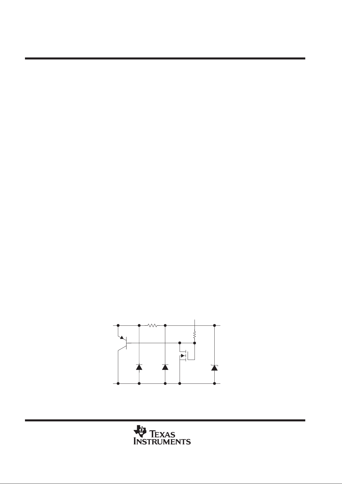
electrostatic discharge
CMOS circuits are prone to gate oxide breakdown when exposed to high voltages even if the exposure is only
for very short periods of time. Electrostatic discharge (ESD) is one of the most common causes of damage to
CMOS devices. It can occur when a device is handled without proper consideration for environmental
electrostatic charges, e.g., during board assembly . If a circuit in which one amplifier from a dual op amp is being
used and the unused pins are left open, high voltages tends to develop. If there is no provision for ESD
protection, these voltages may eventually punch through the gate oxide and cause the device to fail. T o prevent
voltage buildup, each pin is protected by internal circuitry.
Standard ESD-protection circuits safely shunt the ESD current by providing a mechanism whereby one or more
transistors break down at voltages higher than the normal operating voltages but lower than the breakdown
voltage of the input gate. This type of protection scheme is limited by leakage currents which flow through the
shunting transistors during normal operation after an ESD voltage has occurred. Although these currents are
small, on the order of tens of nanoamps, CMOS amplifiers are often specified to draw input currents as low as
tens of picoamps.
To overcome this limitation, TI design engineers developed the patented ESD-protection circuit shown in
Figure 1. This circuit can withstand several successive 2-kV ESD pulses, while reducing or eliminating leakage
currents that may be drawn through the input pins. A more detailed discussion of the operation of the TI
ESD-protection circuit is presented on the next page.
All input and output pins on LinCMOS and Advanced LinCMOS products have associated ESD-protection
circuitry that undergoes qualification testing to withstand 2000 V discharged from a 100-pF capacitor through
a 1500-Ω resistor (human body model) and 200 V from a 100-pF capacitor with no current-limiting resistor
(charged device model). These tests simulate both operator and machine handling of devices during normal
test and assembly operations.
To Protected Circuit
D3
R2
Q2
D2D1
Q1
Input
GND
R1
V
DD
Figure 1. LinCMOS ESD-Protection Schematic

TLC3704, TLC3704Q
QUAD MICROPOWER LinCMOS VOLTAGE COMPARATORS
SLCS117A – NOVEMBER 1986 – REVISED OCT OBER 1996
9
POST OFFICE BOX 655303 • DALLAS, TEXAS 75265
PRINCIPLES OF OPERATION
input protection circuit operation
Texas Instruments patented protection circuitry allows for both positive- and negative-going ESD transients.
These transients are characterized by extremely fast rise times and usually low energies, and can occur both
when the device has all pins open and when it is installed in a circuit.
positive ESD transients
Initial positive charged energy is shunted through Q1 to VSS. Q1 turns on when the voltage at the input rises
above the voltage on the V
DD
pin by a value equal to the VBE of Q1. The base current increases through R2
with input current as Q1 saturates. The base current through R2 forces the voltage at the drain and gate of Q2
to exceed its threshold level (V
T
∼ 22 to 26 V) and turn Q2 on. The shunted input current through Q1 to VSS is
now shunted through the n-channel enhancement-type MOSFET Q2 to V
SS
. If the voltage on the input pin
continues to rise, the breakdown voltage of the zener diode D3 is exceeded and all remaining energy is
dissipated in R1 and D3. The breakdown voltage of D3 is designed to be 24 to 27 V , which is well below the gateoxide voltage of the circuit to be protected.
negative ESD transients
The negative charged ESD transients are shunted directly through D1. Additional energy is dissipated in R1
and D2 as D2 becomes forward biased. The voltage seen by the protected circuit is – 0.3 V to –1 V (the forward
voltage of D1 and D2).
circuit-design considerations
LinCMOS products are being used in actual circuit environments that have input voltages that exceed the
recommended common-mode input voltage range and activate the input protection circuit. Even under normal
operation, these conditions occur during circuit power up or power down, and in many cases, when the device
is being used for a signal conditioning function. The input voltages can exceed V
ICR
and not damage the device
only if the inputs are current limited. The recommended current limit shown on most product data sheets is
± 5 mA. Figures 2 and 3 show typical characteristics for input voltage versus input current.
Normal operation and correct output state can be expected even when the input voltage exceeds the positive
supply voltage. Again, the input current should be externally limited even though internal positive current limiting
is achieved in the input protection circuit by the action of Q1. When Q1 is on, it saturates and limit the current
to approximately 5-mA collector current by design. When saturated, Q1 base current increases with input
current. This base current is forced into the V
DD
pin and into the device IDD or the VDD supply through R2
producing the current limiting effects shown in Figure 2. This internal limiting lasts only as long as the input
voltage is below the V
T
of Q2.
When the input voltage exceeds the negative supply voltage, normal operation is affected and output voltage
states may not be correct. Also, the isolation between channels of multiple devices (duals and quads) can be
severely affected. External current limiting must be used since this current is directly shunted by D1 and D2 and
no internal limiting is achieved. If normal output voltage states are required, an external input voltage clamp is
required (see Figure 4).

TLC3704, TLC3704Q
QUAD MICROPOWER LinCMOS VOLTAGE COMPARATORS
SLCS117A – NOVEMBER 1986 – REVISED OCT OBER 1996
10
POST OFFICE BOX 655303 • DALLAS, TEXAS 75265
PRINCIPLES OF OPERATION
circuit-design considerations (continued)
Figure 2
– Input Current – mA
V
DD
VDD + 4 VDD + 8 VDD + 12
VI – Input Voltage – V
INPUT CURRENT
vs
INPUT VOLTAGE
TA = 25° C
8
7
6
5
4
3
2
1
0
I
I
Figure 3
VDD – 0.3
VI – Input Voltage – V
INPUT CURRENT
vs
INPUT VOLTAGE
TA = 25° C
VDD – 0.5 VDD – 0.7 VDD – 0.9
10
9
8
7
6
5
4
3
2
1
0
– Input Current – mAI
I
+
–
1/2
TLC3704
V
ref
V
I
V
DD
See Note A
R
I
NOTE A: If the correct input state is required when the negative input exceeds GND, a Schottky clamp is required.
Negative Voltage Input Current Limit :
R
I
+
*
V
I
*
VDD*(*
0.3 V)
5mA
RI+
V
I
*
VDD*
0.3 V
5mA
Positive Voltage Input Current Limit :
Figure 4. Typical Input Current-Limiting Configuration for a LinCMOS Comparator

TLC3704, TLC3704Q
QUAD MICROPOWER LinCMOS VOLTAGE COMPARATORS
SLCS117A – NOVEMBER 1986 – REVISED OCT OBER 1996
11
POST OFFICE BOX 655303 • DALLAS, TEXAS 75265
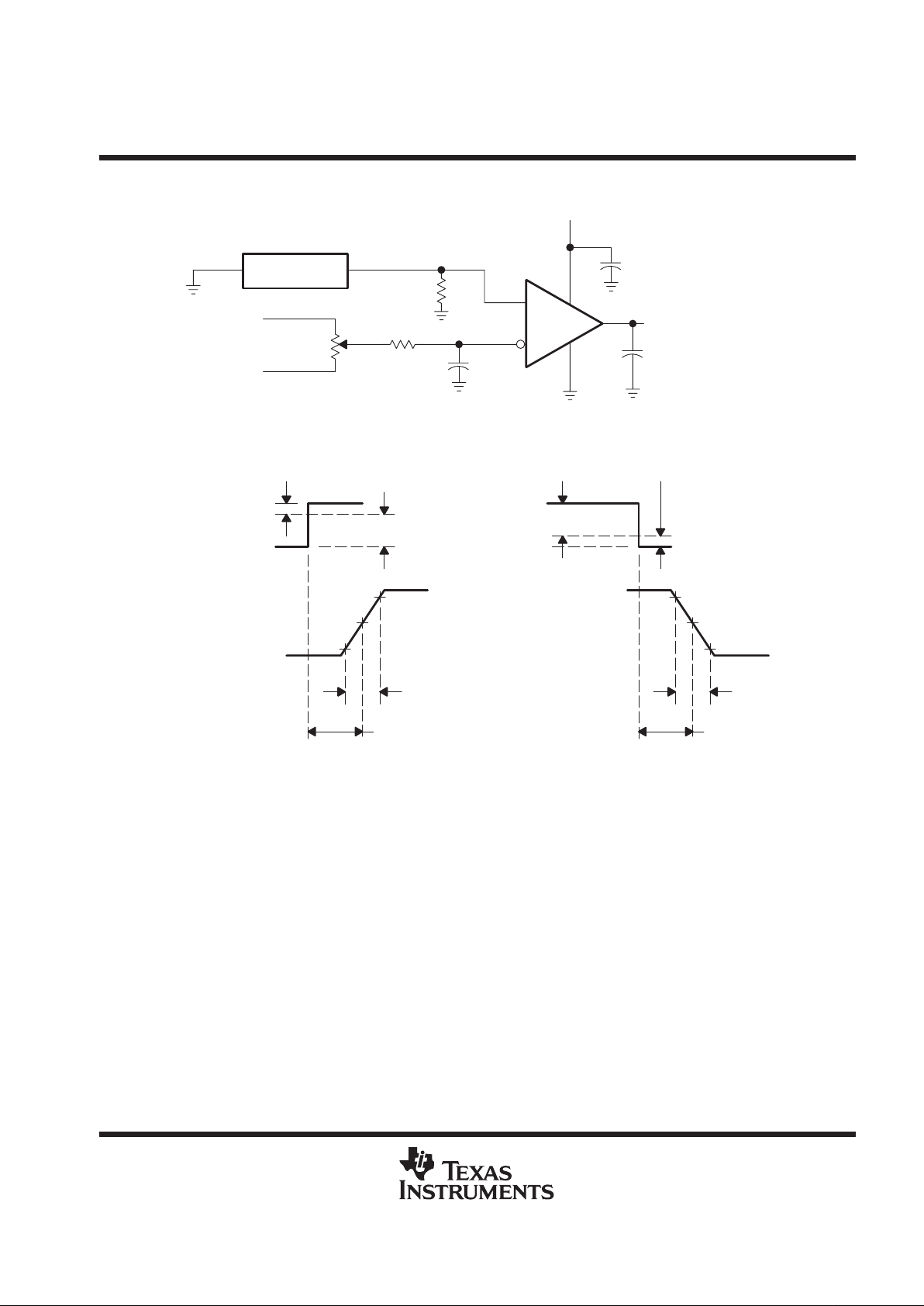
PARAMETER MEASUREMENT INFORMATION
The TLC3704 contains a digital output stage which, if held in the linear region of the transfer curve, can cause
damage to the device. Conventional operational amplifier/comparator testing incorporates the use of a servo
loop which is designed to force the device output to a level within this linear region. Since the servo-loop method
of testing cannot be used, we offer the following alternatives for measuring parameters such as input offset
voltage, common-mode rejection, etc.
T o verify that the input offset voltage falls within the limits specified, the limit value is applied to the input as shown
in Figure 5(a). With the noninverting input positive with respect to the inverting input, the output should be high.
With the input polarity reversed, the output should be low.
A similar test can be made to verify the input offset voltage at the common-mode extremes. The supply voltages
can be slewed as shown in Figure 5(b) for the V
ICR
test, rather than changing the input voltages, to provide
greater accuracy.
+
–
5 V
Applied V
IO
Limit
V
O
+
–
1 V
Applied V
IO
Limit
V
O
– 4 V
(a) VIO WITH VIC = 0 V (b) VIO WITH VIC = 4 V
Figure 5. Method for Verifying That Input Offset Voltage Is Within Specified Limits
A close approximation of the input offset voltage can be obtained by using a binary search method to vary the
differential input voltage while monitoring the output state. When the applied input voltage differential is equal,
but opposite in polarity, to the input offset voltage, the output changes states.
Figure 6 illustrates a practical circuit for direct dc measurement of input offset voltage that does not bias the
comparator in the linear region. The circuit consists of a switching mode servo loop in which IC1a generates
a triangular waveform of approximately 20-mV amplitude. IC1b acts as a buffer , with C2 and R4 removing any
residual d.c. offset. The signal is then applied to the inverting input of the comparator under test, while the
noninverting input is driven by the output of the integrator formed by IC1c through the voltage divider formed
by R8 and R9. The loop reaches a stable operating point when the output of the comparator under test has a
duty cycle of exactly 50%, which can only occur when the incoming triangle wave is sliced symmetrically or when
the voltage at the noninverting input exactly equals the input offset voltage.
Voltage divider R8 and R9 provides an increase in the input offset voltage by a factor of 100 to make
measurement easier. The values of R5, R7, R8, and R9 can significantly influence the accuracy of the reading;
therefore, it is suggested that their tolerance level be one percent or lower.
Measuring the extremely low values of input current requires isolation from all other sources of leakage current
and compensation for the leakage of the test socket and board. With a good picoammeter, the socket and board
leakage can be measured with no device in the socket. Subsequently , this open socket leakage value can be
subtracted from the measurement obtained with a device in the socket to obtain the actual input current of the
device.

TLC3704, TLC3704Q
QUAD MICROPOWER LinCMOS VOLTAGE COMPARATORS
SLCS117A – NOVEMBER 1986 – REVISED OCT OBER 1996
12
POST OFFICE BOX 655303 • DALLAS, TEXAS 75265
PARAMETER MEASUREMENT INFORMATION
–
+
DUT
V
DD
+
–
–
+
–
+
C2
1 µF
R4
47 kΩ
R5
1.8 kΩ 1%
C3
0.68 µF
IC1c
1/4 TLC274CN
IC1a
1/4 TLC274CN
IC1b
1/4 TLC274CN
R6
1 MΩ
R7
1.8 kΩ 1%
R8
10 kΩ 1%
R1
240 kΩ
R2
10 kΩ
C1
0.1 µF
R3
100 Ω
C4
0.1 µF
Integrator
R9
100 Ω 1%
Buffer
Triangle
Generator
V
IO
(X100)
Figure 6. Circuit for Input Offset Voltage Measurement
Response time is defined as the interval between the application of an input step function and the instant when
the output reaches 50% of its maximum value. Response time for the low-to-high-level output is measured from
the leading edge of the input pulse, while response time for the high-to-low-level output is measured from the
trailing edge of the input pulse. Response time measurement at low input signal levels can be greatly affected
by the input offset voltage. The offset voltage should be balanced by the adjustment at the inverting input as
shown in Figure 7, so that the circuit is just at the transition point. A low signal, for example 105-mV or 5-mV
overdrive, causes the output to change state.
TLC3704, TLC3704Q
QUAD MICROPOWER LinCMOS VOLTAGE COMPARATORS
SLCS117A – NOVEMBER 1986 – REVISED OCT OBER 1996
13
POST OFFICE BOX 655303 • DALLAS, TEXAS 75265
PARAMETER MEASUREMENT INFORMATION
+
–
DUT
V
DD
C
L
(see Note A)
Pulse
Generator
10 Ω
10-Turn
Potentiometer
1 V
– 1 V
1 kΩ
50 Ω
1 µF
0.1 µF
TEST CIRCUIT
100 mVInput
Overdrive
90%
50%
10%
t
r
t
PLH
100 mVInput
Overdrive
90%
50%
10%
t
f
t
PHL
Low-to-High
Level Output
High-to-Low
Level Output
VOLTAGE WAVEFORMS
NOTE A: CL includes probe and jig capacitance.
Figure 7. Response, Rise, and Fall Times Circuit and Voltage Waveforms
TLC3704, TLC3704Q
QUAD MICROPOWER LinCMOS VOLTAGE COMPARATORS
SLCS117A – NOVEMBER 1986 – REVISED OCT OBER 1996
14
POST OFFICE BOX 655303 • DALLAS, TEXAS 75265
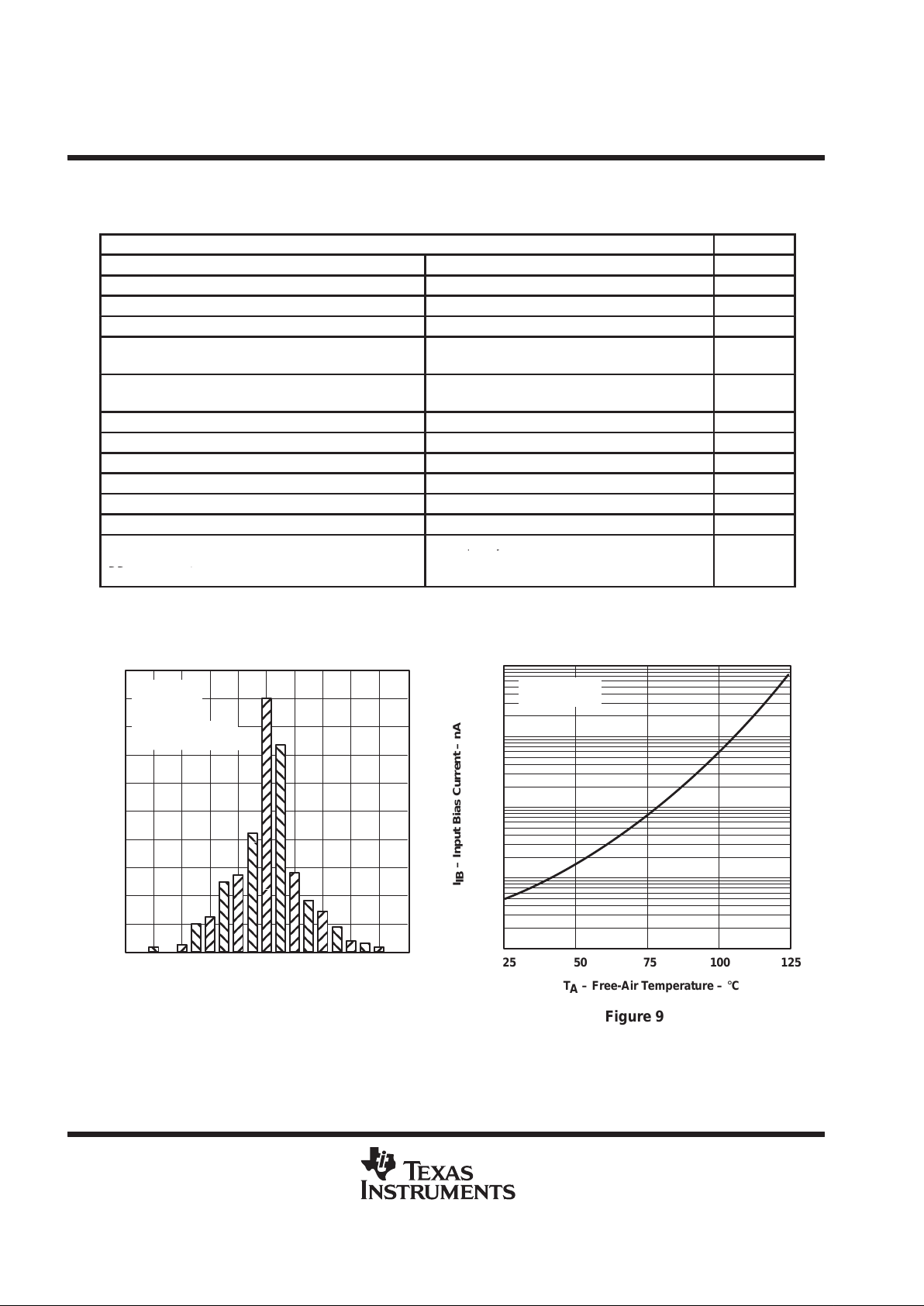
TYPICAL CHARACTERISTICS
Table of Graphs
FIGURE
V
IO
Input offset voltage Distribution 8
I
IB
Input bias current vs Free-air temperature 9
CMRR Common-mode rejection ratio vs Free-air temperature 10
k
SVR
Supply-voltage rejection ratio vs Free-air temperature 11
p
vs Free-air temperature 12
VOHHigh-level output current
vs High-level output current 13
p
vs Low-level output current 14
VOLLow-level output voltage
vs Free-air temperature 15
t
t
Transition time vs Load capacitance 16
Supply current response vs Time 17
Low-to-high-level output response Low-to-high level output propagation delay time 18
High-to-low level output response High-to-low level output propagation delay time 19
t
PLH
Low-to-high level output propagation delay time vs Supply voltage 20
t
PHL
High-to-low level output propagation delay time vs Supply voltage 21
vs Frequency 22
I
DD
Supply current
qy
vs Supply voltage 23
DD
y
g
vs Free-air temperature 24
Figure 8
Number of Units
VDD = 5 V
VIC = 2.5 V
TA = 25° C
–5 –4 –3 –2 –1 0 1 2 3 4 5
VIO – Input Offset Voltage – mV
DISTRIBUTION OF INPUT
OFFSET VOLTAGE
†
200
180
160
140
120
100
80
60
40
20
0
698 Units Tested
From 4 Wafer Lots
Figure 9
I
TA – Free-Air Temperature – °C
IB
– Input Bias Current – nA
25 50 75 100 125
10
1
0.1
0.01
0.001
INPUT BIAS CURRENT
vs
FREE-AIR TEMPERATURE
†
VDD = 5 V
VIC = 2.5 V
†
Data at high and low temperatures are applicable only within the rated operating free-air temperature ranges of the various devices.

TLC3704, TLC3704Q
QUAD MICROPOWER LinCMOS VOLTAGE COMPARATORS
SLCS117A – NOVEMBER 1986 – REVISED OCT OBER 1996
15
POST OFFICE BOX 655303 • DALLAS, TEXAS 75265
TYPICAL CHARACTERISTICS
†
Figure 10
CMRR – Common-Mode Rejection Ratio – dB
TA – Free-Air Temperature – °C
COMMON-MODE REJECTION RATIO
vs
FREE-AIR TEMPERATURE
–75 –50 –25 0 25 50 75 100 125
90
88
86
84
82
80
78
76
74
72
70
VDD = 5 V
Figure 11
–75 –50 –25 0 25 50 75 100 125
k
SVR
– Supply Voltage Rejection Ratio – dB
TA – Free-Air Temperature – °C
SUPPLY VOLTAGE REJECTION RATIO
vs
FREE-AIR TEMPERATURE
VDD = 5 V to 10 V
90
88
86
84
82
80
78
76
74
72
70
Figure 12
5
TA – Free-Air Temperature – °C
HIGH-LEVEL OUTPUT VOLTAGE
vs
FREE-AIR TEMPERATURE
V
OH – High-Level Outout Voltage – V
VDD = 5 V
IOH = – 4 mA
–75 –50 –25 0 25 50 75 100 125
4.9
4.8
4.7
4.6
4.5
4.55
4.65
4.75
4.85
4.95
Figure 13
VDD = 16 V
IOH – High-Level Output Current – mA
HIGH-LEVEL OUTPUT VOLTAGE
vs
HIGH-LEVEL OUTPUT CURRENT
V
OH
TA = 25°C
3 V
4 V
5 V
10 V
0 –2.5 –5 –7.5 –10 –12.5 –15 –17.5 –20
– High-Input Level Output Voltage –V
V
DD
–0.25
–0.5
–0.75
–1
–1.25
–1.5
–1.75
–2
†
Data at high and low temperatures are applicable only within the rated operating free-air temperature ranges of the various devices.

TLC3704, TLC3704Q
QUAD MICROPOWER LinCMOS VOLTAGE COMPARATORS
SLCS117A – NOVEMBER 1986 – REVISED OCT OBER 1996
16
POST OFFICE BOX 655303 • DALLAS, TEXAS 75265
TYPICAL CHARACTERISTICS
†
Figure 14
5 V
IOL – Low-Level Output Current – mA
0 2 4 6 8 1012141618 20
V
OL
– Low-Level Output Voltage – V
LOW-LEVEL OUTPUT VOLTAGE
vs
LOW-LEVEL OUTPUT CURRENT
3 V
10 V
1.5
1.25
1
0.75
0.5
0.25
0
VDD = 16 V
4 V
TA = 25°C
Figure 15
–75 –50 –25 0 25 50 75 100 125
TA – Free-Air Temperature – °C
LOW-LEVEL OUTPUT VOLTAGE
vs
FREE-AIR TEMPERATURE
V
OL
– Low-Level Output Voltage – mV
400
350
300
250
200
150
100
50
0
VDD = 5 V
IOL = 4 mA
Figure 16
0 200 400 600 800 1000
CL – Load Capacitance – pF
t
t
– Transition Time – ns
OUTPUT TRANSITION TIME
vs
LOAD CAPACITANCE
250
225
200
175
150
125
100
75
50
25
0
VDD = 5 V
TA = 25°C
Rise Time
Fall Time
Figure 17
I
DD
– Supply
SUPPLY CURRENT RESPONSE
TO AN OUTPUT VOLTAGE TRANSITION
Current – mA
t – Time
Output
Voltage – V
10
5
0
5
0
VDD = 5 V
CL = 50 pF
f = 10 kHz
†
Data at high and low temperatures are applicable only within the rated operating free-air temperature ranges of the various devices.

TLC3704, TLC3704Q
QUAD MICROPOWER LinCMOS VOLTAGE COMPARATORS
SLCS117A – NOVEMBER 1986 – REVISED OCT OBER 1996
17
POST OFFICE BOX 655303 • DALLAS, TEXAS 75265
TYPICAL CHARACTERISTICS
Figure 18
012345
40 mV
20 mV
10 mV
5 mV
2 mV
V
O
– Output
Voltage – V
Input
Voltage – mV
Differential
LOW-TO-HIGH-LEVEL OUTPUT RESPONSE
FOR VARIOUS INPUT OVERDRIVES
t
PLH
– Low-to-High-Level Output
Response Time – µs
5
0
100
0
VDD = 5 V
TA = 25° C
CL = 50 pF
Figure 19
40 mV
20 mV
10 mV
5 mV
2 mV
HIGH-TO-LOW-LEVEL OUTPUT RESPONSE
FOR VARIOUS INPUT OVERDRIVES
t
PHL
– High-to-Low-Level Output
Response Time – µs
V
O
– Output
Voltage – V
Input
Voltage – mV
Differential
5
0
100
0
012345
VDD = 5 V
TA = 25° C
CL = 50 pF
Figure 20
LOW-TO-HIGH-LEVEL
OUTPUT RESPONSE TIME
vs
SUPPLY VOLTAGE
6
5
4
3
2
1
0
0 24 6 810121416
VDD – Supply Voltage – V
t
PLH
– Low-to-High-Level
Output Response –µs
Overdrive = 2 mV
CL = 50 pF
TA = 25°C
5 mV
10 mV
20 mV
40 mV
Figure 21
HIGH-TO-LOW-LEVEL
OUTPUT RESPONSE TIME
vs
SUPPLY VOLTAGE
6
5
4
3
2
1
0
0 2 4 6 8 10121416
VDD – Supply Voltage – V
t
PHL
– High-to-Low-Level
Output Response –µs
CL = 50 pF
TA = 25°C
5 mV
10 mV
20 mV
40 mV
Overdrive = 2 mV

TLC3704, TLC3704Q
QUAD MICROPOWER LinCMOS VOLTAGE COMPARATORS
SLCS117A – NOVEMBER 1986 – REVISED OCT OBER 1996
18
POST OFFICE BOX 655303 • DALLAS, TEXAS 75265
TYPICAL CHARACTERISTICS
†
Figure 22
AVERAGE SUPPLY CURRENT
(PER COMPARATOR)
vs
FREQUENCY
10000
1000
100
10
V – Average Supply Current – µ
DD
A
0.01 0.1 1 10 100
f – Frequency – kHz
TA = 25°C
CL = 50 pF
VDD = 16 V
10 V
5 V
4 V
3 V
Figure 23
SUPPLY CURRENT
vs
SUPPLY VOLTAGE
VDD – Supply Voltage – V
80
70
60
50
40
30
20
10
0
0246810121416
T
A
= 25°C
TA = 125°C
V – Supply Current – µ
DD
A
TA = – 55°C
TA = 85°C
TA = – 40°C
Outputs Low
No Loads
SUPPLY CURRENT
vs
FREE-AIR TEMPERATURE
30
25
20
15
10
5
0
–75 –50 – 25 0 25 50 75 100 125
TA – Free-Air Temperature – °C
I
DD
– Supply Current –µA
VDD = 5 V
No Load
Outputs Low
Outputs High
Figure 24
†
Data at high and low temperatures are applicable only within the rated operating free-air temperature ranges of the various devices.

TLC3704, TLC3704Q
QUAD MICROPOWER LinCMOS VOLTAGE COMPARATORS
SLCS117A – NOVEMBER 1986 – REVISED OCT OBER 1996
19
POST OFFICE BOX 655303 • DALLAS, TEXAS 75265
APPLICATION INFORMATION
The inputs should always remain within the supply rails in order to avoid forward biasing the diodes in the electrostatic
discharge (ESD) protection structure. If either input exceeds this range, the device is not damaged as long as the
input is limited to less than 5 mA. To maintain the expected output state, the inputs must remain within the
common-mode range. For example, at 25°C with V
DD
= 5 V, both inputs must remain between – 0.2 V and 4 V to
ensure proper device operation. To ensure reliable operation, the supply should be decoupled with a capacitor
(0.1 µF) that is positioned as close to the device as possible.
Output and supply current limitations should be watched carefully since the TLC3704 does not provide current
protection. For example, each output can source or sink a maximum of 20 mA; however, the total current to ground
can only be an absolute maximum of 60 mA. This prohibits sinking 20 mA from each of the four outputs simultaneously
since the total current to ground would be 80 mA.
The TLC3704 has internal ESD-protection circuits that prevents functional failures at voltages up to 2000 V as tested
under MIL-STD-883C, Method 3015.2; however, care should be exercised in handling these devices as exposure
to ESD may result in the degradation of the device parametric performance.
Table of Applications
FIGURE
Pulse-width-modulated motor speed controller 25
Enhanced supply supervisor 26
Two-phase nonoverlapping clock generator 27
Micropower switching regulator 28

TLC3704, TLC3704Q
QUAD MICROPOWER LinCMOS VOLTAGE COMPARATORS
SLCS117A – NOVEMBER 1986 – REVISED OCT OBER 1996
20
POST OFFICE BOX 655303 • DALLAS, TEXAS 75265
APPLICATION INFORMATION
C1
0.01 µF
(see Note B)
5 V
1/2 TLC3704
Motor Speed Control
Potentiometer
+
–
+
–
10 kΩ
100 kΩ
10 kΩ
10 kΩ
See
Note A
1/2 TLC3704
10 kΩ
5 V
DIR
EN
SN75603
Half-H Driver
12 V
Motor
DIR
EN
12 V
Direction
Control
S1
SPDT
5 V
5 V
SN75604
Half-H Driver
NOTES: A. The recommended minimum capacitance is 10 µF to eliminate common ground switching noise.
B. Adjust C1 for change in oscillator frequency
Figure 25. Pulse-Width-Modulated Motor Speed Controller

TLC3704, TLC3704Q
QUAD MICROPOWER LinCMOS VOLTAGE COMPARATORS
SLCS117A – NOVEMBER 1986 – REVISED OCT OBER 1996
21
POST OFFICE BOX 655303 • DALLAS, TEXAS 75265
APPLICATION INFORMATION
1/2 TLC3704
To µP Interrupt
Early Power Fail
+
–
+
–
1 kΩ
3.3 kΩ
C
T
(see Note B)
1/2 TLC3704
10 kΩ
5 V
5 V
12-V
Sense
R2
R1
V
(UNREG)
(see Note A)
1 µF
12 V
RESIN
REF C
T
GND
RESET
SENSEV
CC
To µP
Reset
Monitors 5 VDC Rail
Monitors 12 VDC Rail
Early Power Fail Warning
TL7705A
2.5 V
NOTES: A.
V
(UNREG)
+
2.5
(R1 +R2)
R2
B. The value of CT determines the time delay of reset.
Figure 26. Enhanced Supply Supervisor

TLC3704, TLC3704Q
QUAD MICROPOWER LinCMOS VOLTAGE COMPARATORS
SLCS117A – NOVEMBER 1986 – REVISED OCT OBER 1996
22
POST OFFICE BOX 655303 • DALLAS, TEXAS 75265
APPLICATION INFORMATION
–
+
22 kΩ
C1
0.01 µF
(see Note A)
1/2 TLC3704
R1
100 kΩ
(see Note B)
12 V
100 kΩ
1/2 TLC3704
OUT2
–
+
–
+
1/2 TLC3704
100 kΩ
100 kΩ
12 V
OUT1
12 V
R2
5 kΩ
(see Note C)
R3
100 kΩ
(see Note B)
OUT2
OUT1
12 V
NOTES: A. Adjust C1 for a change in oscillator frequency where:
1/f = 1.85(100 kΩ)C1
B. Adjust R1 and R3 to change duty cycle
C. Adjust R2 to change deadtime
Figure 27. Two-Phase Nonoverlapping Clock Generator

TLC3704, TLC3704Q
QUAD MICROPOWER LinCMOS VOLTAGE COMPARATORS
SLCS117A – NOVEMBER 1986 – REVISED OCT OBER 1996
23
POST OFFICE BOX 655303 • DALLAS, TEXAS 75265
APPLICATION INFORMATION
+
–
100 kΩ
C1
180 µF
(see Note A)
1/2 TLC3704
100 kΩ
R2
100 kΩ
100 kΩ
100 kΩ
V
I
V
I
–
+
1/2 TLC3704
V
I
+
–
TLC271
(see Note B)
270 kΩ
V
I
100 kΩ
C2
100 pF
100 kΩ
R = 6 Ω
L = 1 mH
(see Note D)
R
L
470 µF
V
O
R1
VI+
6 V to 16 V
IL+
0.01 mA to 0.25 mA
VO+
2.5
(R1)R2)
R2
LM385
2.5 V
47 µF
Tantalum
IN5818
V
I
GS
SK9504
(see Note C)
D
+
NOTES: A. Adjust C1 for a change in oscillator frequency
B. TLC271 – Tie pin 8 to pin 7 for low bias operation
C. SK9504 – VDS = 40 V
IDS = 1 A
will
D. To achieve microampere current drive, the inductance of the circuit must be increased.
Figure 28. Micropower Switching Regulator

IMPORTANT NOTICE
T exas Instruments and its subsidiaries (TI) reserve the right to make changes to their products or to discontinue
any product or service without notice, and advise customers to obtain the latest version of relevant information
to verify, before placing orders, that information being relied on is current and complete. All products are sold
subject to the terms and conditions of sale supplied at the time of order acknowledgement, including those
pertaining to warranty, patent infringement, and limitation of liability.
TI warrants performance of its semiconductor products to the specifications applicable at the time of sale in
accordance with TI’s standard warranty. Testing and other quality control techniques are utilized to the extent
TI deems necessary to support this warranty. Specific testing of all parameters of each device is not necessarily
performed, except those mandated by government requirements.
CERT AIN APPLICATIONS USING SEMICONDUCTOR PRODUCTS MAY INVOLVE POTENTIAL RISKS OF
DEATH, PERSONAL INJURY, OR SEVERE PROPERTY OR ENVIRONMENTAL DAMAGE (“CRITICAL
APPLICATIONS”). TI SEMICONDUCTOR PRODUCTS ARE NOT DESIGNED, AUTHORIZED, OR
WARRANTED TO BE SUITABLE FOR USE IN LIFE-SUPPORT DEVICES OR SYSTEMS OR OTHER
CRITICAL APPLICATIONS. INCLUSION OF TI PRODUCTS IN SUCH APPLICA TIONS IS UNDERST OOD TO
BE FULLY AT THE CUSTOMER’S RISK.
In order to minimize risks associated with the customer’s applications, adequate design and operating
safeguards must be provided by the customer to minimize inherent or procedural hazards.
TI assumes no liability for applications assistance or customer product design. TI does not warrant or represent
that any license, either express or implied, is granted under any patent right, copyright, mask work right, or other
intellectual property right of TI covering or relating to any combination, machine, or process in which such
semiconductor products or services might be or are used. TI’s publication of information regarding any third
party’s products or services does not constitute TI’s approval, warranty or endorsement thereof.
Copyright 1998, Texas Instruments Incorporated
 Loading...