TEXAS INSTRUMENTS THS3120, THS3121 Technical data
www.ti.com
0
0.01
0.02
0.03
0.04
0.05
0.06
0.07
0 1 2 3 4 5 6 7 8
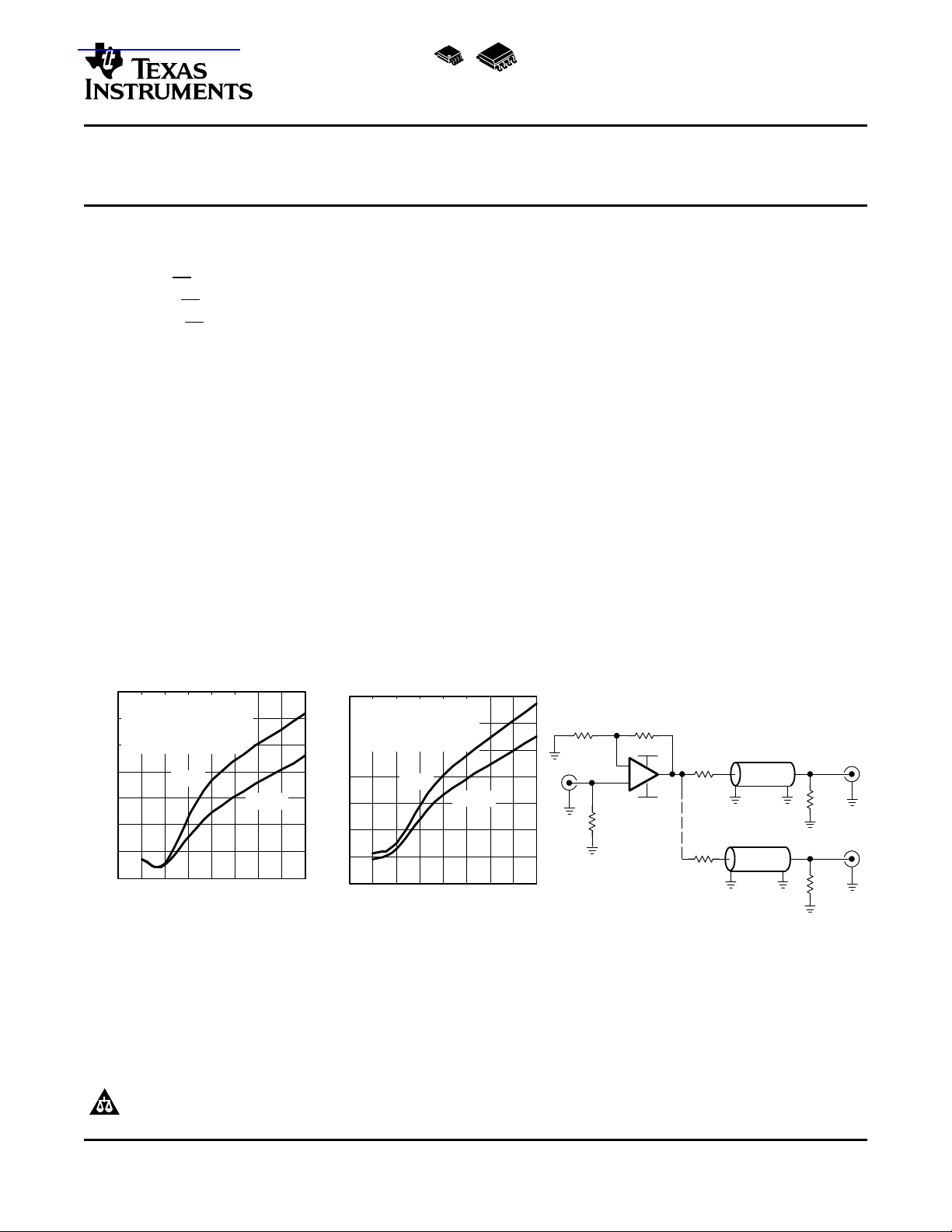
Number of 150 Ω Loads
Differential Gain − %
PAL
NTSC
Gain = 2,
RF = 649 Ω,
VS = ±15 V,
40 IRE − NTSC and PAL,
Worst Case ±100 IRE Ramp
+
−
75 Ω
75 Ω
75 Ω
75 Ω
75 Ω
n Lines
V
O(1)
V
O(n)
75-Ω Transmission Line
V
I
649 Ω 649 Ω
−15 V
15 V
0
0.02
0.04
0.06
0.08
0.1
0.12
0.14
0 1 2 3 4 5 6 7 8
Number of 150 Ω Loads
Differential Phase − deg
PAL
NTSC
Gain = 2,
RF = 649 Ω,
VS = ±15 V,
40 IRE − NTSC and PAL,
Worst Case ±100 IRE Ramp
DIFFERENTIAL PHASE
vs
NUMBER OF LOADS
DIFFERENTIAL GAIN
vs
NUMBER OF LOADS
VIDEO DISTRIBUTION AMPLIFIER APPLICATION
查询THS3120供应商
LOW-NOISE, HIGH-OUTPUT DRIVE, CURRENT-FEEDBACK,
FEATURES DESCRIPTION
• Low Noise
– 1 pA/ √ Hz Noninverting Current Noise
– 10 pA/ √ Hz Inverting Current Noise
– 2.5 nV/ √ Hz Voltage Noise
• High Output Current Drive: 475 mA
• High Slew Rate: 1700 V/ µs (R
V
= 8 V
O
)
PP
• Wide Bandwidth: 120 MHz (G = 2, R
• Wide Supply Range: ± 5 V to ± 15 V
• Power-Down Feature: (THS3120 Only)
APPLICATIONS
• Video Distribution
• Power FET Driver
• Pin Driver
• Capacitive Load Driver
= 50 Ω,
L
THS3120, THS3121
SLOS420A – SEPTEMBER 2003 – REVISED NOVEMBER 2003
OPERATIONAL AMPLIFIERS
The THS3120 and THS3121 are low-noise,
high-voltage, high output current drive, currentfeedback amplifiers designed to operate over a wide
supply range of ± 5 V to ± 15 V for today's high
performance applications.
The THS3120 offers a power saving mode by providing a power-down pin for reducing the 7-mA quiescent current of the device, when the device is not
= 50 Ω)
L
active.
These amplifiers provide well-regulated ac
performance characteristics. Most notably, the 0.1-dB
flat bandwidth is exceedingly high, reaching beyond
90 MHz. The unity gain bandwidth of 130 MHz allows
for good distortion characteristics at 10 MHz. Coupled
with high 1700-V/ µs slew rate, the THS3120 and
THS3121 amplifiers allow for high output voltage
swings at high frequencies.
The THS3120 and THS3121 are offered in a 8-pin
SOIC (D), and the 8-pin MSOP (DGN) packages with
PowerPAD™.
PowerPAD is a trademark of Texas Instruments.
PRODUCTION DATA information is current as of publication date.
Products conform to specifications per the terms of the Texas
Instruments standard warranty. Production processing does not
necessarily include testing of all parameters.
Please be aware that an important notice concerning availability, standard warranty, and use in critical applications of Texas
Instruments semiconductor products and disclaimers thereto appears at the end of this data sheet.
Copyright © 2003, Texas Instruments Incorporated
www.ti.com
1
2
3
4
8
7
6
5
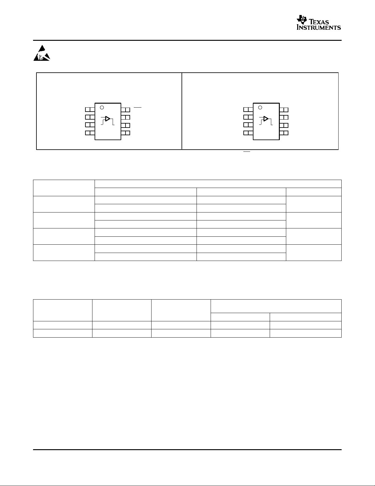
NC
V
IN−
V
IN+
V
S−
NC
V
S+
V
OUT
NC
D, DGNTOP VIEWD, DGNTOP VIEW
NC = No Internal Connection
1
2
3
4
8
7
6
5
REF
V
IN−
V
IN+
V
S−
PD
V
S+
V
OUT
NC
NC = No Internal Connection
THS3120 THS3121
Note: The device with the power down option defaults to the ON state if no signal is applied to the PD pin. Additionallly, the REF pin
functional range is from VS− to (VS+ − 4 V).
THS3120, THS3121
SLOS420A – SEPTEMBER 2003 – REVISED NOVEMBER 2003
This integrated circuit can be damaged by ESD. Texas Instruments recommends that all integrated circuits be handled with
appropriate precautions. Failure to observe proper handling procedures and installation procedures can cause damage.
AVAILABLE OPTIONS
T
A
0 ° C to 70 ° C AQA
-40 ° C to 85 ° C APN
0 ° C to 70 ° C AQO
-40 ° C to 85 ° C APO
(1) Available in tape and reel. The R suffix standard quantity is 2500 (e.g. THS3120CDGNR).
(2) The PowerPAD is electrically isolated from all other pins.
PLASTIC SMALL OUTLINE SOIC (D) PLASTIC MSOP (DGN)
THS3120CD THS3120CDGN
THS3120CDR THS3120CDGNR
THS3120ID THS3120IDGN
THS3120IDR THS3120IDGNR
THS3121CD THS3121CDGN
THS3121CDR THS3121CDGNR
THS3121ID THS3121IDGN
THS3121IDR THS3121IDGNR
PACKAGED DEVICE
(1) (2)
SYMBOL
DISSIPATION RATING TABLE
POWER RATING
TJ= 125 ° C
PACKAGE Θ
(1)
D-8
(2)
DGN-8
(1) This data was taken using the JEDEC standard low-K test PCB. For the JEDEC proposed high-K test PCB, the Θ
power rating at TA= 25 ° C of 1.05 W.
(2) This data was taken using 2 oz. trace and copper pad that is soldered directly to a 3 inch x 3 inch PCB. For further information, refer to
the Application Information section of this data sheet.
( ° C/W) Θ
JC
38.3 95 1.05 W 421 mW
4.7 58.4 1.71 W 685 W
( ° C/W)
JA
TA= 25 ° C TA= 85 ° C
2
JA
is 95 ° C/W with
www.ti.com
THS3120, THS3121
SLOS420A – SEPTEMBER 2003 – REVISED NOVEMBER 2003
RECOMMENDED OPERATING CONDITIONS
MIN NOM MAX UNIT
Supply voltage V
Operating free-air temperature, T
A
Operating junction temperature, continuous operating, T
Normal storage temperature, T
stg
ABSOLUTE MAXIMUM RATINGS
over operating free-air temperature (unless otherwise noted)
Supply voltage, VS-to V
Input voltage, V
Differential input voltage, V
Output current, I
Continuous power dissipation See Dissipation Ratings Table
Maximum junction temperature, T
Maximum junction temperature, continuous operation, long term reliability, T
Operating free-air temperature, T
Storage temperature, T
Lead temperature 1,6 mm (1/16 inch) from case for 10 seconds 300 ° C
ESD ratings:
(1) Stresses beyond those listed under absolute maximum ratings may cause permanent damage to the device. These are stress ratings
only, and functional operation of the device at these or any other conditions beyond those indicated under, , recommended operating
conditions” is not implied. Exposure to absolute-maximum-rated conditions for extended periods may affect device reliability.
(2) The THS3120 and THS3121 may incorporate a PowerPAD™ on the underside of the chip. This acts as a heatsink and must be
connected to a thermally dissipating plane for proper power dissipation. Failure to do so may result in exceeding the maximum junction
temperature which could permanently damage the device. See TI Technical Brief SLMA002 for more information about utilizing the
PowerPAD™ thermally enhanced package.
(3) The absolute maximum temperature under any condition is limited by the constraints of the silicon process.
(4) The maximum junction temperature for continuous operation is limited by the package constraints. Operation above this temperature
may result in reduced reliability and/or lifetime of the device.
S+
I
(2)
O
ID
(3)
J
A
stg
HBM 1000
CDM 1500
MM 200
Dual supply ± 5 ± 15
Single supply 10 30
Commercial 0 70
Industrial -40 85
J
-40 125 ° C
-40 85 ° C
(1)
550 mA
150 ° C
(4)
J
125 ° C
Commercial 0 ° C to 70 ° C
Industrial -40 ° C to 85 ° C
-65 ° C to 125 ° C
UNIT
± 4 V
33 V
± V
S
° C
3

www.ti.com
THS3120, THS3121
SLOS420A – SEPTEMBER 2003 – REVISED NOVEMBER 2003
ELECTRICAL CHARACTERISTICS
VS= ±15 V, RF= 649 Ω,R
PARAMETER TEST CONDITIONS
AC PERFORMANCE
Small-signal bandwidth, -3 dB
0.1 dB bandwidth flatness G = 2, RF= 649 Ω , VO= 200 mV
Large-signal bandwidth G = 5, RF= 499 Ω , VO= 2 V
Slew rate (25% to 75% level) V/µs TYP
Slew rate 900 V/µs MAX
Rise and fall time G = -5, VO= 10-V step, RF= 499 Ω 10 ns TYP
Settling time to 0.1% G = -2, VO= 2 VPPstep 11
Settling time to 0.01% G = -2, VO= 2 VPPstep 52
Harmonic distortion
2nd Harmonic distortion
3rd Harmonic distortion
Input voltage noise f > 20 kHz 2.5 nV / √ Hz TYP
Noninverting input current noise f > 20 kHz 1 pA / √ Hz TYP
Inverting input current noise f > 20 kHz 10 pA / √ Hz TYP
Differential gain
Differential phase
DC PERFORMANCE
Transimpedance VO= ± 3.75 V, Gain = 1 1.9 1.3 1 1 M Ω MIN
Input offset voltage 2 6 8 8 mV MAX
Average offset voltage drift ± 10 ± 10 µV/ ° C TYP
Noninverting input bias current 1 4 6 6 µA MAX
Average bias current drift ± 10 ± 10 nA/ ° C TYP
Inverting input bias current 3 15 20 20 µA MAX
Average bias current drift ± 10 ± 10 nA/ ° C TYP
Input offset current 4 15 20 20 µA MAX
Average offset current drift ± 30 ± 30 nA/ ° C TYP
INPUT CHARACTERISTICS
Input common-mode voltage range ± 13.3 ± 13 ± 12.8 ± 12.8 V MIN
Common-mode rejection ratio VCM= ± 12.5 V 70 63 60 60 dB MIN
Noninverting input resistance 41 M Ω TYP
Noninverting input capacitance 0.4 pF TYP
OUTPUT CHARACTERISTICS
Output voltage swing V MIN
Output current (sourcing) RL= 25 Ω 475 425 400 400 mA MIN
Output current (sinking) RL= 25 Ω 490 425 400 400 mA MIN
Output impedance f = 1 MHz, Closed loop 0.04 Ω TYP
= 50 Ω, and G = 2 (unless otherwise noted)
L
TYP OVER TEMPERATURE
25 ° C 25 ° C UNIT
G = 1, RF= 806 Ω , VO= 200 mV
G = 2, RF= 649 Ω , VO= 200 mV
G = 5, RF= 499 Ω , VO= 200 mV
G = 10, RF= 301 Ω , VO= 200 mV
G = 1, VO= 4-V step, RF= 806 Ω 1500
G = 2, VO= 8-V step, RF= 649 Ω 1700
Recommended maximum SR for
repetitive signals
G = 2,
RF= 649 Ω ,
VO= 2 VPP,
f = 10 MHz
G = 2,
RL= 150 Ω , TYP
RF= 649 Ω
VCM= 0 V
VCM= 0 V
VCM= 0 V
VCM= 0 V
RL= 1 k Ω ± 14 ± 13.5 ± 13 ± 13
RL= 50 Ω ± 13.5 ± 12.5 ± 12 ± 12
(1)
PP
PP
PP
PP
PP
PP
RL= 50 Ω 51
RL= 499 Ω 53
RL= 50 Ω 50
RL= 499 Ω 65
NTSC 0.007%
PAL 0.007%
NTSC 0.018 °
PAL 0.022 °
130
120
105
66
90
80
0 ° C to -40 ° C to MIN/TYP/
70 ° C 85 ° C MAX
MHz TYP
ns TYP
dBc TYP
(1) For more information, see the Application Information section of this data sheet.
4
www.ti.com
THS3120, THS3121
SLOS420A – SEPTEMBER 2003 – REVISED NOVEMBER 2003
ELECTRICAL CHARACTERISTICS (continued)
VS= ±15 V, RF= 649 Ω,R
PARAMETER TEST CONDITIONS
POWER SUPPLY
Specified operating voltage ± 15 ± 16 ± 16 ± 16 V MAX
Maximum quiescent current 7 8.5 11 11 mA MAX
Minimum quiescent current 7 5.5 4 4 mA MIN
Power supply rejection (+PSRR) VS+= 15.5 V to 14.5 V, VS-= 15 V 83 75 70 70 dB MIN
Power supply rejection (-PSRR) VS+= 15 V, VS-= -15.5 V to -14.5 V 78 70 65 65 dB MIN
POWER-DOWN CHARACTERISTICS
Power-down voltage level V MAX
Power-down quiescent current PD = 0V 300 450 500 500 µA MAX
VPDquiescent current µA TYP
Turnon time delay 90% of final value 4
Turnoff time delay 10% of final value 6
Input impedance 3.4 || 1.7 k Ω || pF TYP
= 50 Ω, and G = 2 (unless otherwise noted)
L
Enable, REF = 0 V ≤ 0.8
Power-down , REF = 0 V ≥ 2
VPD= 0 V, REF = 0 V, 11
VPD= 3.3 V, REF = 0 V 11
TYP OVER TEMPERATURE
25 ° C 25 ° C UNIT
0 ° C to -40 ° C to MIN/TYP/
70 ° C 85 ° C MAX
µs TYP
5
www.ti.com
THS3120, THS3121
SLOS420A – SEPTEMBER 2003 – REVISED NOVEMBER 2003
ELECTRICAL CHARACTERISTICS
VS= ±5 V, RF= 750 Ω, RL= 50 Ω, and G = 2 (unless otherwise noted)
TYP OVER TEMPERATURE
PARAMETER TEST CONDITIONS
AC PERFORMANCE
G = 1, RF= 909 Ω , VO= 200 mV
Small-signal bandwidth, -3 dB
0.1 dB bandwidth flatness G = 2, RF= 750 Ω , VO= 200 mV
Large-signal bandwidth G = 2, RF= 750 Ω , VO= 2 V
Slew rate (25% to 75% level) V/µs TYP
Slew rate 900 V/µs MAX
Rise and fall time G = -5, VO= 5-V step, RF= 499 Ω 10 ns TYP
Settling time to 0.1% G = -2, VO= 2 VPPstep 7
Settling time to 0.01% G = -2, VO= 2 VPPstep 42
Harmonic distortion
2nd Harmonic distortion
3rd Harmonic distortion
Input voltage noise f > 20 kHz 2.5 nV / √ Hz TYP
Noninverting input current noise f > 20 kHz 1 pA / √ Hz TYP
Inverting input current noise f > 20 kHz 10 pA / √ Hz TYP
Differential gain
Differential phase
DC PERFORMANCE
Transimpedance VO= ± 1.25 V, Gain = 1 1.2 0.9 0.7 0.7 M Ω MIN
Input offset voltage 3 6 8 8 mV MAX
Average offset voltage drift ± 10 ± 10 µV/ ° C TYP
Noninverting input bias current 1 4 6 6 µA MAX
Average bias current drift ± 10 ± 10 nA/ ° C TYP
Inverting input bias current 2 15 20 20 µA MAX
Average bias current drift ± 10 ± 10 nA/ ° C TYP
Input offset current 2 15 20 20 µA MAX
Average offset current drift ± 30 ± 30 nA/ ° C TYP
INPUT CHARACTERISTICS
Input common-mode voltage range ± 3.2 ± 2.9 ± 2.8 ± 2.8 V MIN
Common-mode rejection ratio VCM= ± 2.5 V 66 62 58 58 dB MIN
Noninverting input resistance 35 M Ω TYP
Noninverting input capacitance 0.5 pF TYP
OUTPUT CHARACTERISTICS
Output voltage swing V MIN
Output current (sourcing) RL= 10 Ω 310 250 200 200 mA MIN
Output current (sinking) RL= 10 Ω 325 250 200 200 mA MIN
Output impedance f = 1 MHz 0.05 Ω TYP
G = 2, RF= 750 Ω , VO= 200 mV
G = 5, RF= 499 Ω , VO= 200 mV
G = 10, RF= 301 Ω , VO= 200 mV
G = 1, VO= 2-V step, RF= 909 Ω 560
G = 2, VO= 2-V step, RF= 750 Ω 620
Recommended maximum SR for
repetitive signals
G = 2,
RF= 649 Ω ,
VO= 2 VPP,
f = 10 MHz
G = 2,
RL= 150 Ω , TYP
RF= 806 Ω
VCM= 0 V
VCM= 0 V
VCM= 0 V
VCM= 0 V
RL= 1 k Ω ± 4 ± 3.8 ± 3.7 ± 3.7
RL= 50 Ω ± 3.9 ± 3.7 ± 3.6 ± 3.6
(1)
PP
PP
PP
PP
PP
PP
RL= 50 Ω 51
RL= 499 Ω 53
RL= 50 Ω 48
RL= 499 Ω 60
NTSC 0.008%
PAL 0.008%
NTSC 0.014 °
PAL 0.018 °
25 ° C 25 ° C UNIT
105
100
95
70
70
85
0 ° C to -40 ° C to MIN/TYP/
70 ° C 85 ° C MAX
MHz TYP
ns TYP
dBc TYP
(1) For more information, see the Application Information section of this data sheet.
6

www.ti.com
THS3120, THS3121
SLOS420A – SEPTEMBER 2003 – REVISED NOVEMBER 2003
ELECTRICAL CHARACTERISTICS (continued)
VS= ±5 V, RF= 750 Ω, RL= 50 Ω, and G = 2 (unless otherwise noted)
TYP OVER TEMPERATURE
PARAMETER TEST CONDITIONS
POWER SUPPLY
Specified operating voltage ± 5 ± 4.5 ± 4.5 ± 4.5 V MIN
Maximum quiescent current 6.5 8 10 10 mA MAX
Minimum quiescent current 6.5 4 3.5 3.5 mA MIN
Power supply rejection (+PSRR) 80 72 67 67 dB MIN
Power supply rejection (-PSRR) 75 67 62 62 dB MIN
POWER-DOWN CHARACTERISTICS
Power-down voltage level V MAX
Power-down quiescent current PD = 0 V 200 450 500 500 µA MAX
VPDquiescent current µA TYP
Turnon time delay 90% of final value 4
Turnoff time delay 10% of final value 6
Input impedance 3.4 || 1.7 k Ω || pF TYP
VS+= 5.5 V to 4.5 V,
VS-= 5 V
VS+= 5 V,
VS-= -5.5 V to -4.5 V
Enable, REF = 0 V ≤ 0.8
Power-down , REF = 0 V ≥ 0.2
VPD= 0 V, REF = 0 V, 11
VPD= 3.3 V, REF = 0 V 11
25 ° C 25 ° C UNIT
0 ° C to -40 ° C to MIN/TYP/
70 ° C 85 ° C MAX
µs TYP
7
www.ti.com
THS3120, THS3121
SLOS420A – SEPTEMBER 2003 – REVISED NOVEMBER 2003
TYPICAL CHARACTERISTICS
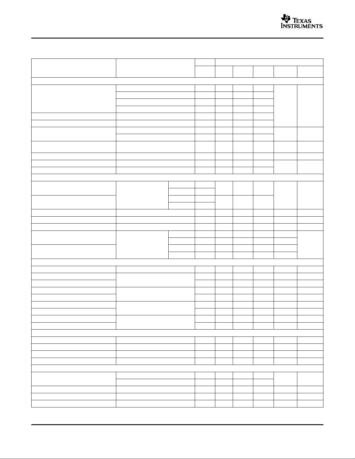
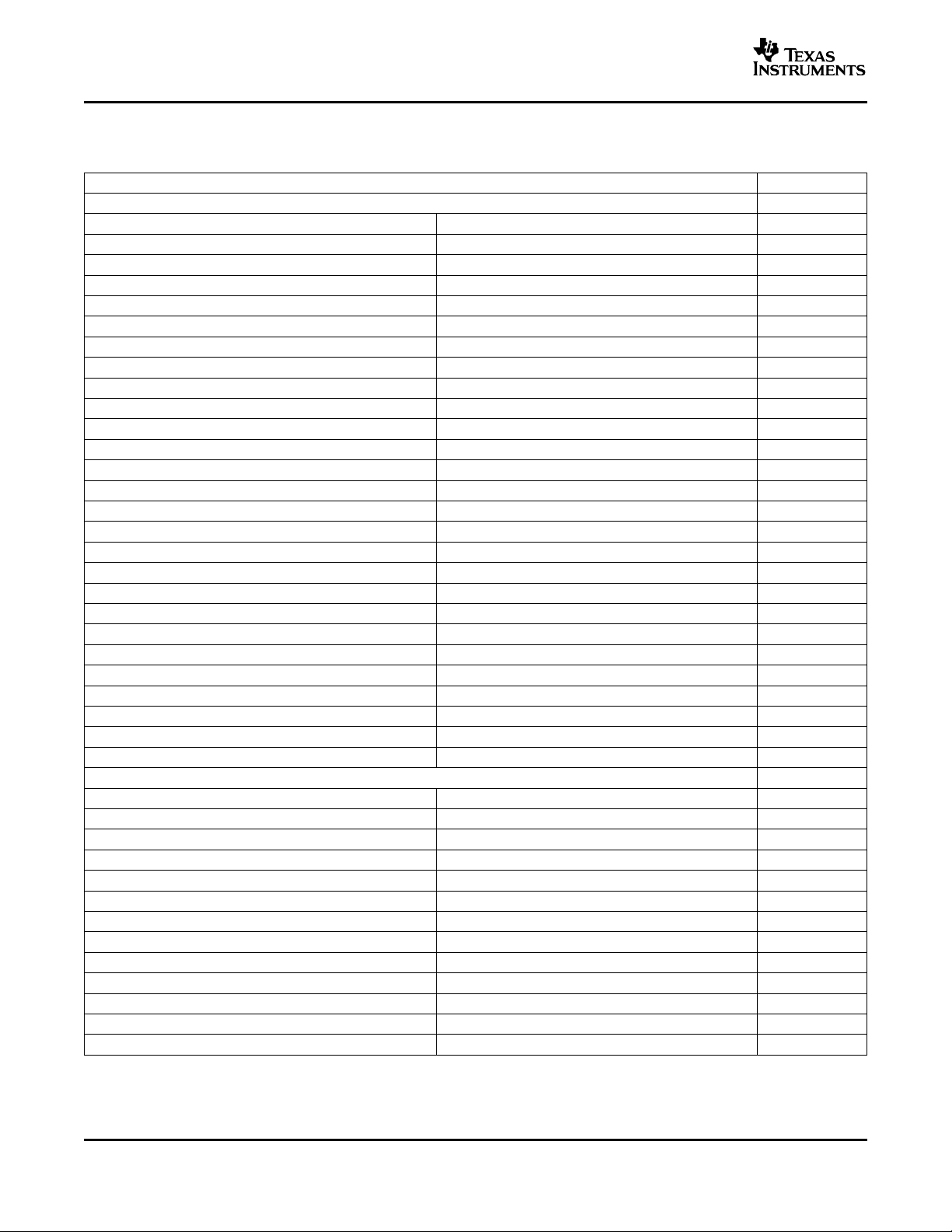
TABLE OF GRAPHS
± 15-V graphs
Noninverting small signal gain frequency response 1, 2
Inverting small signal gain frequency response 3
0.1 dB flatness 4
Noninverting large signal gain frequency response 5
Inverting large signal gain frequency response 6
Frequency response capacitive load 7
Recommended R
2nd Harmonic distortion vs Frequency 9
3rd Harmonic distortion vs Frequency 10
Harmonic distortion vs Output voltage swing 11, 12
Slew rate vs Output voltage step 13, 14
Noise vs Frequency 15
Settling time 16, 17
Quiescent current vs Supply voltage 18
Output voltage vs Load resistance 19
Input bias and offset current vs Case temperature 20
Input offset voltage vs Case temperature 21
Transimpedance vs Frequency 22
Rejection ratio vs Frequency 23
Noninverting small signal transient response 24
Inverting large signal transient response 25
Overdrive recovery time 26
Differential gain vs Number of loads 27
Differential phase vs Number of loads 28
Closed loop output impedance vs Frequency 29
Power-down quiescent current vs Supply voltage 30
Turnon and turnoff time delay 31
± 5-V graphs
Noninverting small signal gain frequency response 32
Inverting small signal gain frequency response 33
0.1 dB flatness 34
Slew rate vs Output voltage step 35, 36
2nd Harmonic distortion vs Frequency 37
3rd Harmonic distortion vs Frequency 38
Harmonic distortion vs Output voltage swing 39, 40
Noninverting small signal transient response 41
Inverting small signal transient response 42
Input bias and offset current vs Case temperature 43
Overdrive recovery time 44
Settling time 45
Rejection ratio vs Frequency 46
ISO
vs Capacitive load 8
FIGURE
8
www.ti.com
0
1
2
3
4
5
6
7
8
9
1 M 10 M 100 M 1 G
f − Frequency − Hz
Noninverting Gain − dB
RF = 475 Ω
RF = 649 Ω
RF = 750 Ω
Gain = 2,
RL = 50 Ω,
VO = 0.2 VPP,
VS = ±15 V
−4
−2
0
2
4
6
8
10
12
14
16
18
20
22
24
100 k 1 M 10 M 100 M 1 G
f − Frequency − Hz
Noninverting Gain − dB
G = 1, RF = 806 Ω
G = 10, RF = 301 Ω
G = 5, RF = 499 Ω
G = 2, RF = 649 Ω
RL = 50 Ω,
VO = 0.2 VPP,
VS = ±15 V
-4
-2
0
2
4
6
8
10
12
14
16
18
20
22
24
100 k 1 M 10 M 100 M 1 G
f - Frequency - Hz
Inverting Gain - dB
G = -1, RF = 681 Ω
G = -10, RF = 365 Ω
G = -5, RF = 499 Ω
G = -2, RF = 681 Ω
RL = 50 Ω,
VO = 0.2 VPP,
VS = ±15 V
0
2
4
6
8
10
12
14
16
100 k 1 M 10 M 100 M 1 G
f − Frequency − Hz
Noninverting Gain − dB
G = 5, RF = 499 Ω
G = 2, RF = 681 Ω
RL = 50 Ω,
VO = 2 VPP,
VS = ±15 V
5.7
5.8
5.9
6
6.1
6.2
6.3
100 k 1 M 10 M 100 M
Gain = 2,
RF = 562 Ω,
RL = 50 Ω,
VO = 0.2 VPP,
VS = ±15 V
f - Frequency - Hz
Noninverting Gain - dB
-4
-2
0
2
4
6
8
10
12
14
16
1 M 10 M 100 M 1 G
f - Frequency - Hz
G = -5, RF = 499 Ω
G =-1, RF = 681 Ω
RL = 50 Ω,
VO = 2 VPP,
VS = ±15 V
Inverting Gain - dB
-2
0
2
4
6
8
10
12
14
16
10 M 100 M
Capacitive Load - Hz
Signal Gain - dB
Gain = 5,
RL = 50 Ω
VS = ±15 V
R
(ISO)
= 49.9 Ω CL = 10 pF
R
(ISO)
= 40.2 Ω
CL = 22 pF
R
(ISO)
= 30 Ω
CL = 47 pF
R
(ISO)
= 20 Ω
CL = 100 pF
0
10
20
30
40
50
60
10 100
C
L
− Capacitive Load − pF
Recommended R Ω
Gain = 5,
RL = 50 Ω,
VS = ±15 V
ISO
Resistance −
-90
-80
-70
-60
-50
-40
-30
1 M 10 M 100 M
f - Frequency - Hz
2 nd Harmonic Distortion - dBc
G = 2,
RF = 649 Ω
G = 2, RF = 649 Ω,
RL = 499 Ω
VO = 2 VPP,
RL = 50 Ω,
VS = ±15 V
G = 5,
RF = 499 Ω
-100
100 k
THS3120, THS3121
SLOS420A – SEPTEMBER 2003 – REVISED NOVEMBER 2003
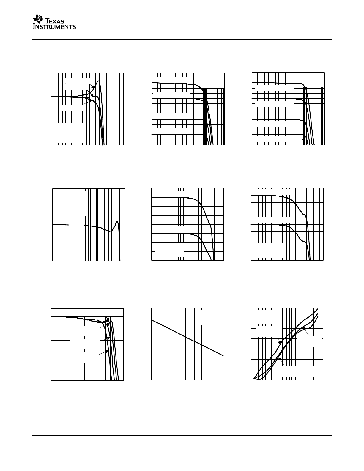
TYPICAL CHARACTERISTICS ( ±15 V)
NONINVERTING SMALL SIGNAL NONINVERTING SMALL SIGNAL INVERTING SMALL SIGNAL
FREQUENCY RESPONSE FREQUENCY RESPONSE FREQUENCY RESPONSE
Figure 1. Figure 2. Figure 3.
0.1 dB FLATNESS FREQUENCY RESPONSE FREQUENCY RESPONSE
NONINVERTING LARGE SIGNAL INVERTING LARGE SIGNAL
Figure 4. Figure 5. Figure 6.
FREQUENCY RESPONSE vs vs
RECOMMENDED R
ISO
2nd HARMONIC DISTORTION
CAPACITIVE LOAD CAPACITIVE LOAD FREQUENCY
Figure 7. Figure 8. Figure 9.
9
 Loading...