

查询THS1408-EP供应商
14-BIT, 1/3/8 MSPS DSP COMPATIBLE ANALOG-TO-DIGITAL CONVERTERS
features
D
Controlled Baseline
– One Assembly/Test Site, One Fabrication
Site
D
Extended Temperature Performance up to
–55°C to 125°C
D
Enhanced Diminishing Manufacturing
Sources (DMS) Support
D
Enhanced Product Change Notification
D
Qualification Pedigree
D
14-Bit Resolution
D
1, 3, and 8 MSPS Speed Grades
D
Differential Nonlinearity (DNL) ±0.6 LSB Typ
†
Component qualification in accordance with JEDEC and industry
standards to ensure reliable operation over an extended
temperature range. This includes, but is not limited to, Highly
Accelerated Stress Test (HAST) or biased 85/85, temperature
cycle, autoclave or unbiased HAST, electromigration, bond
intermetallic life, and mold compound life. Such qualification
testing should not be viewed as justifying use of this component
beyond specified performance and environmental limits.
†
D
D
D
D
D
D
D
D
D
applications
D
D
D
D
D
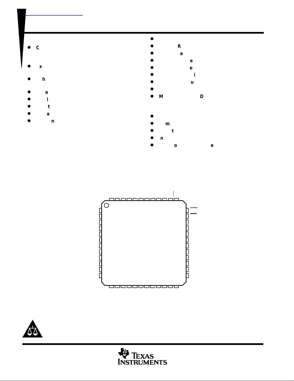
PHP PACKAGE
(TOP VIEW)
THS1401-EP THS1403-EP THS1408-EP
WITH INTERNAL REFERENCE AND PGA
SGLS129A – JULY 2002 – REVISED NOVEMBER 2002
Integral Nonlinearity (INL) ±1.5 LSB Typ
Internal Reference
Differential Inputs
Programmable Gain Amplifier
µP Compatible Parallel Interface
Timing Compatible With TMS320C6000 DSP
3.3-V Single Supply
Power-Down Mode
Monolithic CMOS Design
xDSL Front Ends
Communication
Industrial Control
Instrumentation
Automotive and Selected Military
DD
IN+AVAGND
47 46 45 44 4348 42
IN–
1
AV
VBG
CML
REF+
REF–
AGND
AGND
DGND
NC – No internal connection
Please be aware that an important notice concerning availability, standard warranty, and use in critical applications of
Texas Instruments semiconductor products and disclaimers thereto appears at the end of this data sheet.
DD
OV
D13
D12
2
3
4
5
6
7
8
9
10
11
12
13
14 15
D11
DD
DV
16
DGND
DD
AV
AGND
AGND
17 18 19 20
D9D8D7
D10
DD
A0A1NC
DV
40 39 3841
21 22 23 24
DD
DV
D5D4D3
D6
NC
37
CS
36
35
34
33
32
31
30
29
28
27
26
25
WR
OE
DGND
DGND
CLK
DV
DD
DV
DD
D0
D1
D2
DV
DD
DGND
PRODUCTION DATA information is current as of publication date.
Products conform to specifications per the terms of Texas Instruments
standard warranty. Production processing does not necessarily include
testing of all parameters.
POST OFFICE BOX 655303 • DALLAS, TEXAS 75265
Copyright 2002, Texas Instruments Incorporated
1
THS1401-EP THS1403-EP THS1408-EP
14-BIT, 1/3/8 MSPS DSP COMPATIBLE ANALOG-TO-DIGITAL CONVERTERS
WITH INTERNAL REFERENCE AND PGA
SGLS129A – JULY 2002 – REVISED NOVEMBER 2002
description
The THS1401, THS1403, and THS1408 are 14-bit, 1/3/8 MSPS, single supply analog-to-digital converters with an
internal reference, differential inputs, programmable input gain, and an on-chip sample and hold amplifier.
Implemented with a CMOS process, the device has outstanding price/performance and power/speed ratios. The
THS1401, THS1403, and THS1408 are designed for use with 3.3-V systems, and with a high-speed µP compatible
parallel interface, making them the first choice for solutions based on high-performance DSPs like the TI
TMS320C6000 series.
ORDERING INFORMA TION
–40°C to 125°C PQFP – PHP THS1401QPHPEP THS1401QE
–40°C to 125°C PQFP – PHP THS1403QPHPEP THS1403QE
–55°C to 125°C PQFP – PHP THS1408MPHPEP THS1408ME
†
Package drawings, standard packing quantities, thermal data, symbolization, and PCB design
guidelines are available at www.ti.com/sc/package.
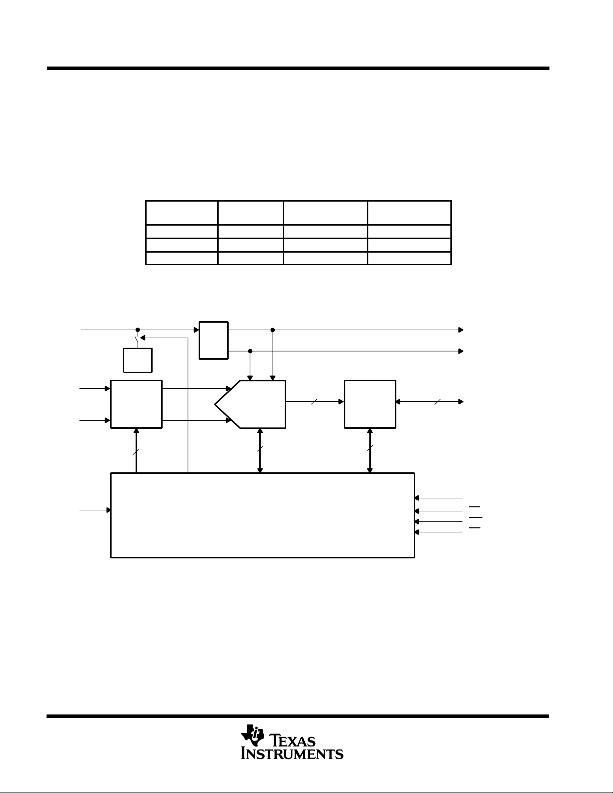
functional block diagram
T
A
PACKAGE
†
ORDERABLE
PART NUMBER
TOP-SIDE
MARKING
VBG
IN+
IN–
CLK
1.5 V
BG
PGA
0..7 dB
REF+
REF
14-Bit
ADC
6
CONTROL
LOGIC
14 15
Buffer
REF–
D[13:0] + OV bit
A[1:0]
CS
WR
OE
2
POST OFFICE BOX 655303 • DALLAS, TEXAS 75265
THS1401-EP THS1403-EP THS1408-EP
I/O
DESCRIPTION
14-BIT, 1/3/8 MSPS DSP COMPATIBLE ANALOG-TO-DIGITAL CONVERTERS
WITH INTERNAL REFERENCE AND PGA
SGLS129A – JULY 2002 – REVISED NOVEMBER 2002
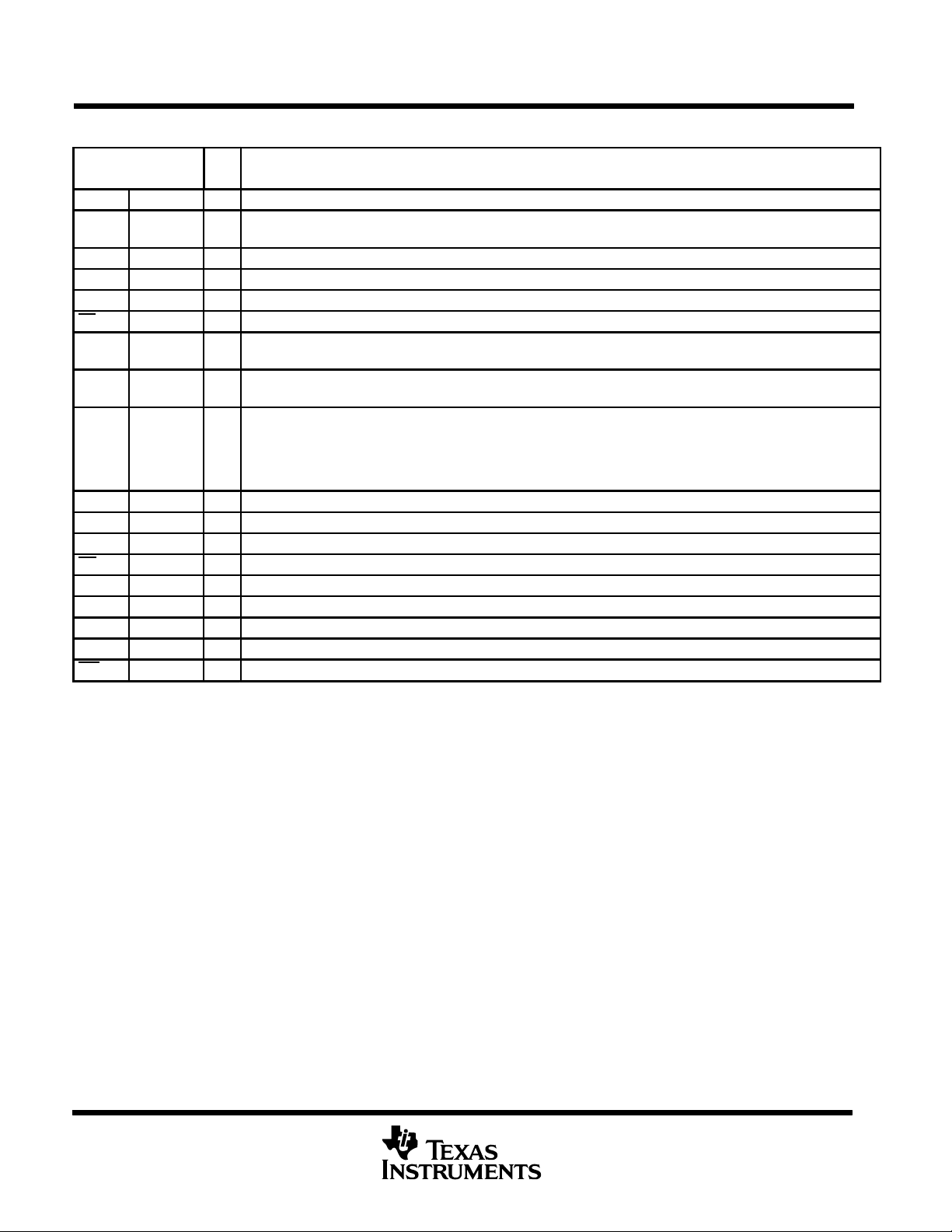
Terminal Functions
TERMINAL
NAME NO.
A[1:0] 40, 41 I Address input
AGND 7,8, 44,
AV
DD
CLK 32 I Clock input
CML 4 Reference midpoint. This pin requires a 0.1-µF capacitor to AGND.
CS 37 I Chip select input. Active low
DGND 9, 15, 25,
DV
DD
D[13:0] 11, 12, 13,
NC 38, 39 No connection, do not use. Reserved
IN+ 48 I Positive differential analog input
IN– 1 I Negative dif ferential analog input
OE 35 I Output enable. Active low
OV 10 O Out of range output
REF+ 5 O Positive reference output. This pin requires a 0.1-µF capacitor to AGND.
REF– 6 O Negative reference output. This pin requires a 0.1-µF capacitor to AGND.
VBG 3 I Reference input. This pin requires a 1-µF capacitor to AGND.
WR 36 I Write signal. Active low
45, 46
2, 43, 47 Analog power supply
33, 34
14, 20, 26,
30, 31, 42
16, 17, 18,
19, 21, 22,
23, 24, 27,
28, 29
Analog ground
Digital ground
Digital power supply
I/O Data inputs/outputs
POST OFFICE BOX 655303 • DALLAS, TEXAS 75265
3
THS1401-EP THS1403-EP THS1408-EP
Operating free-air temperature
°C
14-BIT, 1/3/8 MSPS DSP COMPATIBLE ANALOG-TO-DIGITAL CONVERTERS
WITH INTERNAL REFERENCE AND PGA
SGLS129A – JULY 2002 – REVISED NOVEMBER 2002
absolute maximum ratings over operating free-air temperature (unless otherwise noted)
Supply voltage, (AV
Supply voltage, (DV
Reference input voltage range, VBG – 0.3 V to AV
Analog input voltage range – 0.3 V to AV
Digital input voltage range – 0.3 V to DV
Operating free-air temperature range, T
to AGND) 4V. . . . . . . . . . . . . . . . . . . . . . . . . . . . . . . . . . . . . . . . . . . . . . . . . . . . . . . . . . . . .
DD
to DGND) 4V. . . . . . . . . . . . . . . . . . . . . . . . . . . . . . . . . . . . . . . . . . . . . . . . . . . . . . . . . . . . .
DD
: Q suffix –40°C to 125°C. . . . . . . . . . . . . . . . . . . . . . . . . . . . . . . . . . .
A
†
DD
DD
DD
+ 0.3 V. . . . . . . . . . . . . . . . . . . . . . . . . . . . . . . . . . . . . . .
+ 0.3 V. . . . . . . . . . . . . . . . . . . . . . . . . . . . . . . . . . . . . . . . . . . . . . . . .
+ 0.3 V. . . . . . . . . . . . . . . . . . . . . . . . . . . . . . . . . . . . . . . . . . . . . . . . .
M suffix –55°C to 125°C. . . . . . . . . . . . . . . . . . . . . . . . . . . . . . . . . . .
Storage temperature range, T
stg
–65°C to 150°C. . . . . . . . . . . . . . . . . . . . . . . . . . . . . . . . . . . . . . . . . . . . . . . . . . .
Lead temperature 1.6 mm (1/16 inch) from case for 10 seconds 260°C. . . . . . . . . . . . . . . . . . . . . . . . . . . . . . . .
†
Stresses beyond those listed under “absolute maximum ratings” may cause permanent damage to the device. These are stress ratings only, and
functional operation of the device at these or any other conditions beyond those indicated under “recommended operating conditions” is not implied.
Exposure to absolute-maximum-rated conditions for extended periods may affect device reliability.
THERMAL CHARACTERISTICS
TYP UNIT
Thermal resistance, junction-to-ambient, Θ
Thermal resistance, junction-to-case, Θ
†
Thermal resistance is modeled data, is not production tested, and is given for informational purposes only.
JA
JC
28.8 °C/W
0.79 °C/W
recommended operating conditions
MIN NOM MAX UNIT
Supply voltage, AVDD, DV
High level digital input, V
Low level digital input, V
Load capacitance, C
Clock frequency, f
Clock duty cycle 45% 50% 55%
p
CLK
DD
IH
IL
L
THS1401 0.1 1 1 MHz
THS1403 0.1 3 3 MHz
THS1408 0.1 8 8 MHz
p
Q suffix –40 25 125
M suffix –55 25 125
3 3.3 3.6 V
2 3.3 V
0
0.8
5 15 pF
V
4
POST OFFICE BOX 655303 • DALLAS, TEXAS 75265
THS1401-EP THS1403-EP THS1408-EP
14-BIT, 1/3/8 MSPS DSP COMPATIBLE ANALOG-TO-DIGITAL CONVERTERS
WITH INTERNAL REFERENCE AND PGA
SGLS129A – JULY 2002 – REVISED NOVEMBER 2002
electrical characteristics over recommended operating free-air temperature range,
AVDD = DVDD = 3.3 V (unless otherwise noted)
PARAMETER TEST CONDITIONS MIN TYP MAX UNIT
Power Supply
I
DDA
I
DDD
DC Characteristics
DNL Differential nonlinearity ±0.6 ±1 LSB
INL Integral nonlinearity
AC Characteristics
ENOB Effective number of bits 11.2 11.5 Bits
THD Total harmonic distortion
SNR Signal-to-noise ratio
SINAD Signal-to-noise ratio + distortion
SFDR Spurious free dynamic range
Analog supply current AVDD = 3.6 V 81 90 mA
Digital supply current DVDD = 3.6 V 5 10 mA
Power AVDD = DVDD = 3.6 V 270 360 mW
Power down current 20 µA
Resolution 14 Bits
THS1401 ±1.5 ±2.5
THS1403
THS1408 ±3.5 ±7.5
Offset error IN+ = IN–, PGA = 0 dB 0.3 %FSR
Gain error PGA = 0 dB 1.75 %FSR
THS1401/3/8 fi = 100 kHz –81
THS1403/8
THS1408 fi = 4 MHz –77
THS1401/3/8 fi = 100 kHz 72
THS1403/8
THS1408 fi = 4 MHz 71
THS1401/3/8 fi = 100 kHz 70
THS1403/8
THS1408 fi = 4 MHz 70
THS1401/3/8 fi = 100 kHz 80
THS1403, THS1408
THS1408 fi = 4 MHz 80
Analog input bandwidth 140 MHz
Best fit
fi = 1 MHz –78
fi = 1 MHz 70 72
fi = 1 MHz 69 70
fi = 1 MHz 71 80
±2 ±3
LSB
dB
dB
dB
dB
POST OFFICE BOX 655303 • DALLAS, TEXAS 75265
5
THS1401-EP THS1403-EP THS1408-EP
VBG
14-BIT, 1/3/8 MSPS DSP COMPATIBLE ANALOG-TO-DIGITAL CONVERTERS
WITH INTERNAL REFERENCE AND PGA
SGLS129A – JULY 2002 – REVISED NOVEMBER 2002
electrical characteristics over recommended operating free-air temperature range,
AVDD = DVDD = 3.3 V (unless otherwise noted) (continued)
PARAMETER TEST CONDITIONS MIN TYP MAX UNIT
Reference Voltage
Bandgap voltage, internal mode 1.425 1.5 1.575 V
Input impedance 40 kΩ
Positive reference voltage, REF+ 2.5 V
Negative reference voltage, REF– 0.5 V
Reference difference, ∆REF, REF+ – REF– 2 V
Accuracy, internal reference 5%
Temperature coefficient 40 ppm/°C
Voltage coefficient 200 ppm/V
Analog Inputs
Positive analog input, IN+ 0 AV
Negative analog input, IN– 0 AV
Analog input voltage difference ∆Ain = IN+ – IN–, V
Input impedance 25 kΩ
PGA range 0 7 dB
PGA step size 1 dB
PGA gain error ±0.25 dB
Digital Inputs
V
IH
V
IL
Digital Outputs
V
OH
V
OL
I
OZ
Clock Timing (CS low)
f
CLK
t
d
†
This parameter is not production tested.
High-level digital input 2 V
Low-level digital input 0.8 V
Input capacitance 5 pF
Input current ±1 µA
High-level digital output IOH = 50 µA 2.6 V
Low-level digital output IOL = 50 µA 0.4 V
Output current, high impedance ±10 µA
Clock frequency
Output delay time 25 ns
Latency 9.5 Cycles
THS1401 0.1
THS1403
THS1408 0.1
= REF+ – REF– –V
ref
0.1
ref
†
†
†
ref
V
V
V
DD
DD
V
1 1 MHz
3 3 MHz
8 8 MHz
6
POST OFFICE BOX 655303 • DALLAS, TEXAS 75265
THS1401-EP THS1403-EP THS1408-EP
14-BIT, 1/3/8 MSPS DSP COMPATIBLE ANALOG-TO-DIGITAL CONVERTERS
WITH INTERNAL REFERENCE AND PGA
SGLS129A – JULY 2002 – REVISED NOVEMBER 2002
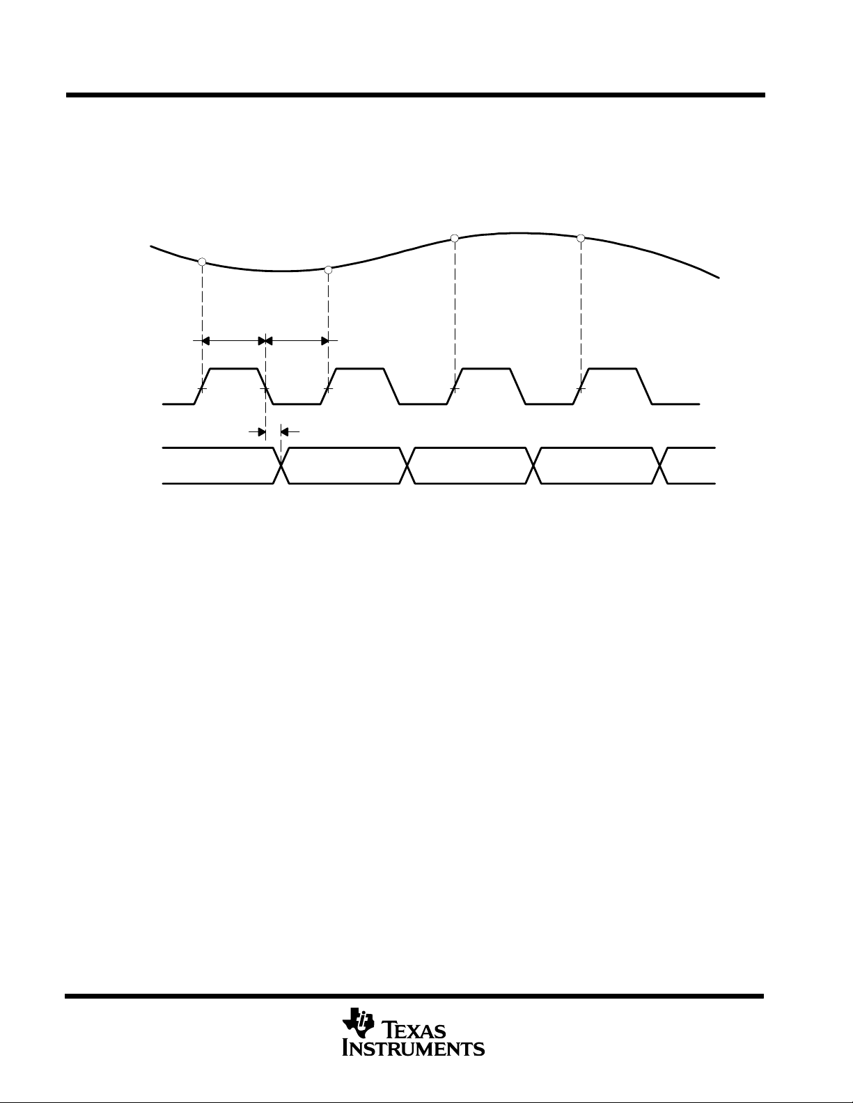
PARAMETER MEASUREMENT INFORMATION
sample timing
The THS1401/3/8 core is based on a pipeline architecture with a latency of 9.5 samples. The conversion results
appear on the digital output 9.5 clock cycles after the input signal was sampled.
Analog
Input
S9
S11
S10
S12
CLK
Data
Out
t
w(CLK)
t
t
w(CLK)
d
C1 C2
C3
Figure 1. Sample Timing
The parallel interface of the THS1401/3/8 ADC features 3-state buffers, making it possible to directly connect it to
a data bus. The output buffers are enabled by driving the OE input low.
Besides the sample results, it is also possible to read back the values of the control register, the PGA register, and
the offset register . Which register is read is determined by the address inputs A[1,0]. The ADC results are available
at address 0.
The timing of the control signals is described in the following sections.
POST OFFICE BOX 655303 • DALLAS, TEXAS 75265
7

THS1401-EP THS1403-EP THS1408-EP
14-BIT, 1/3/8 MSPS DSP COMPATIBLE ANALOG-TO-DIGITAL CONVERTERS
WITH INTERNAL REFERENCE AND PGA
SGLS129A – JULY 2002 – REVISED NOVEMBER 2002
PARAMETER MEASUREMENT INFORMATION
read timing (15-pF load)
PARAMETER MIN TYP MAX UNIT
t
su(OE–ACS)
t
en
t
dis
t
h(A)
t
h(CS)
NOTE: All timing parameters refer to a 50% level.
CS
OE
Address and chip select setup time 4 ns
Output enable 15 ns
Output disable 10 ns
Address hold time 1 ns
Chip select hold time 0 ns
t
h(CS)
D[13:0]
O V
A[1:0]
t
su(OE–ACS)
X X
t
en
DATA
ADDRESS
Figure 2. Read Timing
t
h(A)
t
dis
8
POST OFFICE BOX 655303 • DALLAS, TEXAS 75265

14-BIT, 1/3/8 MSPS DSP COMPATIBLE ANALOG-TO-DIGITAL CONVERTERS
PARAMETER MEASUREMENT INFORMATION
write timing (15-pF load)
t
su(WE–CS)
t
su(DA)
t
h(DA)
t
h(CS)
t
wH(WE)
NOTE: All timing parameters refer to a 50% level.
CS
WE
Chip select setup time 4 ns
Data and address setup time 29 ns
Data and address hold time 0 ns
Chip select hold time 0 ns
Write pulse duration high 15 ns
t
su(WE–CS)
THS1401-EP THS1403-EP THS1408-EP
WITH INTERNAL REFERENCE AND PGA
SGLS129A – JULY 2002 – REVISED NOVEMBER 2002
PARAMETER MIN TYP MAX UNIT
t
h(CS)
t
su(DA)
D[13:0]
t
h(DA)
X
X
A
X X
DATA
ADDRESS
Figure 3. Write Timing
POST OFFICE BOX 655303 • DALLAS, TEXAS 75265
9

THS1401-EP THS1403-EP THS1408-EP
14-BIT, 1/3/8 MSPS DSP COMPATIBLE ANALOG-TO-DIGITAL CONVERTERS
WITH INTERNAL REFERENCE AND PGA
SGLS129A – JULY 2002 – REVISED NOVEMBER 2002
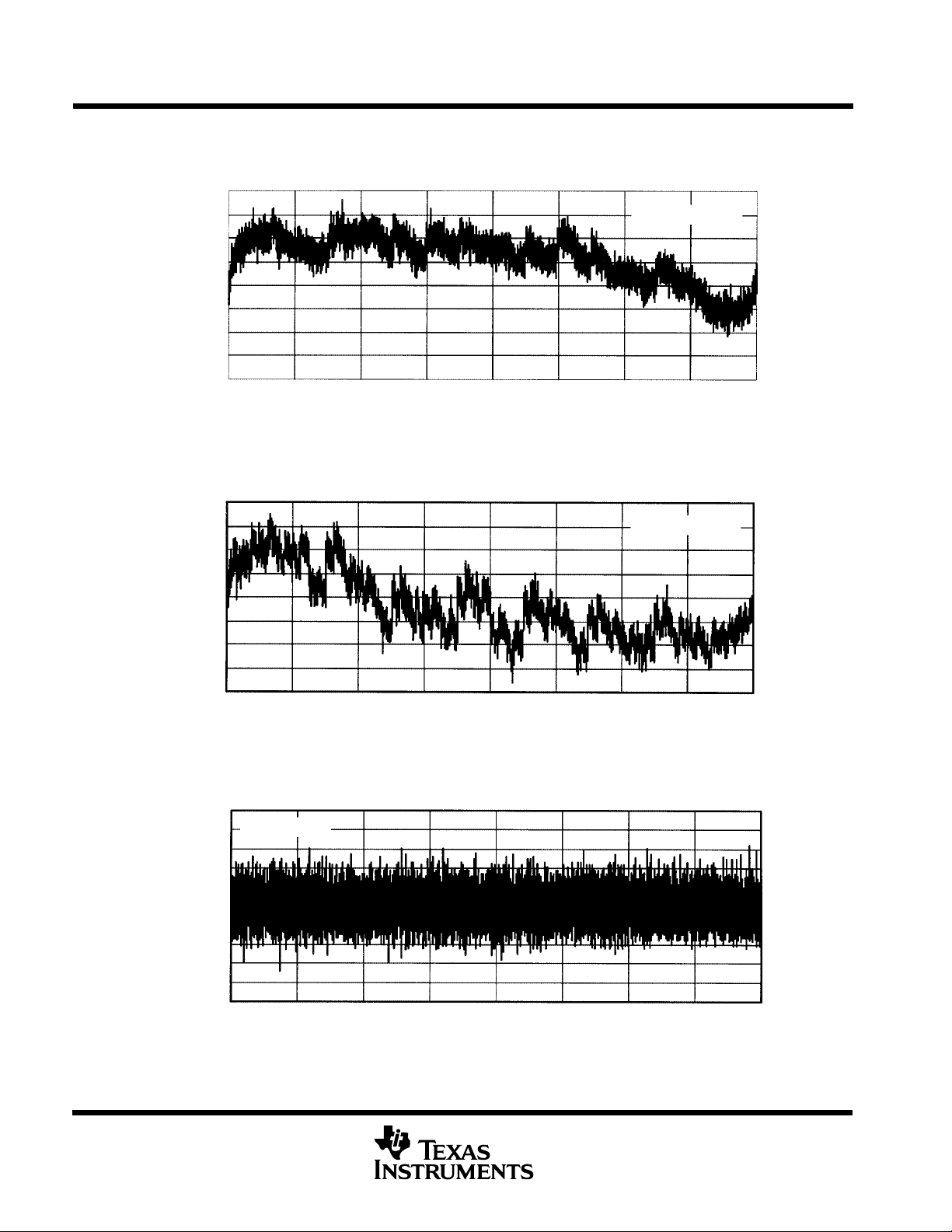
TYPICAL CHARACTERISTICS
POWER
vs
FREQUENCY
284
282
280
278
276
Power – mW
274
272
270
268
0.1 1 10
f – Frequency – MHz
Figure 4
0
fs = 1 MSPS,
–20
fI = 100 kHz,
–1 dB
–40
–60
90
80
70
60
50
40
30
– Supply Current – mA
CC
I
20
10
0
0 50 100 150 200 250 300
FAST FOURIER TRANSFORM
SUPPLY CURRENT
vs
TIME
t – Time – ns
Figure 5
10
–80
Output – dB
–100
–120
–140
0 100 200 300
f – Frequency – kHz
Figure 6
POST OFFICE BOX 655303 • DALLAS, TEXAS 75265
400 500

THS1401-EP THS1403-EP THS1408-EP
14-BIT, 1/3/8 MSPS DSP COMPATIBLE ANALOG-TO-DIGITAL CONVERTERS
WITH INTERNAL REFERENCE AND PGA
SGLS129A – JULY 2002 – REVISED NOVEMBER 2002
TYPICAL CHARACTERISTICS
FAST FOURIER TRANSFORM
0
fs = 3 MSPS,
–20
fI = 1 MHz,
–1 dB
–40
–60
–80
Output – dB
–100
–120
–140
0.1 0.4 0.7 1
f – Frequency – MHz
Figure 7
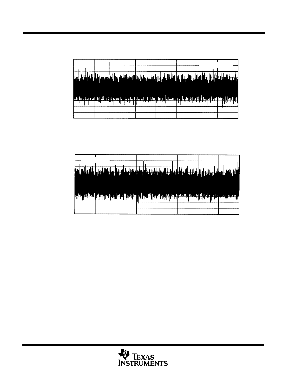
FAST FOURIER TRANSFORM
0
fs = 8 MSPS,
–20
fI = 1 MHz,
–1 dB
–40
–60
1.3
–80
Output – dB
–100
–120
–140
0.1 0.4 0.7 1 1.6 1.9 2.5
1.3
f – Frequency – MHz
Figure 8
INTEGRAL NONLINEARITY
2
fs = 1 MSPS
1
0
0 2048 4096 6144 8192 10240
INL – Integral Nonlinearity – LSB
1.5
0.5
–0.5
–1
–1.5
–2
Figure 9
2.2
Samples
2.8 3.1 3.7 4
12288 14336 16384
3.4
POST OFFICE BOX 655303 • DALLAS, TEXAS 75265
11
THS1401-EP THS1403-EP THS1408-EP
14-BIT, 1/3/8 MSPS DSP COMPATIBLE ANALOG-TO-DIGITAL CONVERTERS
WITH INTERNAL REFERENCE AND PGA
SGLS129A – JULY 2002 – REVISED NOVEMBER 2002
TYPICAL CHARACTERISTICS
INTEGRAL NONLINEARITY
2
1.5
1
0.5
0
–0.5
–1
–1.5
–2
INL – Integral Nonlinearity – LSB
0 2048 4096 6144 8192 10240
Samples
Figure 10
INTEGRAL NONLINEARITY
4
3
2
1
0
–1
–2
–3
–4
INL – Integral Nonlinearity – LSB
0 2048 4096 6144 8192 10240
Samples
fs = 3 MSPS
12288 14336 16384
fs = 8 MSPS
12288 14336 16384
12
Figure 11
DIFFERENTIAL NONLINEARITY
1
fs = 1 MSPS
0.8
0.6
0.4
0.2
0
–0.2
–0.4
–0.6
–0.8
–1
0 2048 4096 6144 8192 10240
DNL – Differential Nonlinearity – LSB
Samples
Figure 12
POST OFFICE BOX 655303 • DALLAS, TEXAS 75265
12288 14336 16384
THS1401-EP THS1403-EP THS1408-EP
14-BIT, 1/3/8 MSPS DSP COMPATIBLE ANALOG-TO-DIGITAL CONVERTERS
WITH INTERNAL REFERENCE AND PGA
SGLS129A – JULY 2002 – REVISED NOVEMBER 2002
TYPICAL CHARACTERISTICS
DIFFERENTIAL NONLINEARITY
1
0.8
0.6
0.4
0.2
0
–0.2
–0.4
–0.6
–0.8
–1
0 2048 4096 6144 8192 10240
DNL – Differential Nonlinearity – LSB
Samples
Figure 13
DIFFERENTIAL NONLINEARITY
1
0.8
0.6
0.4
0.2
–0.2
–0.4
–0.6
–0.8
–1
DNL – Differential Nonlinearity – LSB
fs = 8 MSPS
0
0 2048 4096 6144 8192 10240
Samples
fs = 3 MSPS
12288 14336 16384
12288 14336 16384
Figure 14
POST OFFICE BOX 655303 • DALLAS, TEXAS 75265
13

THS1401-EP THS1403-EP THS1408-EP
14-BIT, 1/3/8 MSPS DSP COMPATIBLE ANALOG-TO-DIGITAL CONVERTERS
WITH INTERNAL REFERENCE AND PGA
SGLS129A – JULY 2002 – REVISED NOVEMBER 2002
TYPICAL CHARACTERISTICS
THD – Total Harmonic Distortion – dB
–70
–72
–74
–76
–78
–80
–82
–84
–86
–88
–90
10
80
78
TOTAL HARMONIC DISTORTION
vs
FREQUENCY
fs = 3 MSPS,
fI at –1 dB
100 1000
f – Frequency – Hz
Figure 15
SIGNAL-TO-NOISE RATIO
vs
FREQUENCY
fs = 3 MSPS,
fI at –1 dB
1500
–70
fs = 8 MSPS,
fI at –1 dB
–72
–74
–76
–78
–80
–82
–84
–86
THD – Total Harmonic Distortion – dB
–88
–90
10 100
80
fs = 8 MSPS,
78
fI at –1 dB
TOTAL HARMONIC DISTORTION
vs
FREQUENCY
1000
f – Frequency – Hz
Figure 16
SIGNAL-TO-NOISE RATIO
vs
FREQUENCY
4000
SNR – Signal-to-Noise Ratio – dB
76
74
72
70
68
66
64
62
60
10
100
f – Frequency – Hz
Figure 17
1000
1500
SNR – Signal-to-Noise Ratio – dB
76
74
72
70
68
66
64
62
60
10
100
f – Frequency – Hz
Figure 18
1000
4000
14
POST OFFICE BOX 655303 • DALLAS, TEXAS 75265

THS1401-EP THS1403-EP THS1408-EP
14-BIT, 1/3/8 MSPS DSP COMPATIBLE ANALOG-TO-DIGITAL CONVERTERS
WITH INTERNAL REFERENCE AND PGA
SGLS129A – JULY 2002 – REVISED NOVEMBER 2002
PRINCIPLES OF OPERATION
registers
The device contains several registers. The A register is selected by the values of bits A1 and A0:
A1 A0 Register
0 0 Conversion result
0 1 PGA
1 0 Offset
1 1 Control
Tables 1 and 2 describe how to read the conversion results and how to configure the data converter. The default
values (were applicable) show the state after a power-on reset.
Table 1. Conversion Result Register, Address 0, Read
BIT D13 D12 D11 D10 D9 D8 D7 D6 D5 D4 D3 D2 D1 D0
Function MSB ... … … … … … … … … … … … LSB
The output can be configured for two’s complement or straight binary format (see D11/control register).
The output code is given by:
2s complement: Straight binary:
–8192 at ∆IN = –∆REF 0 at ∆IN = –∆REF
0 at ∆IN = 0 8192 at ∆IN = 0
8191 ∆IN = –∆REF – 1 LSB 16383 at ∆IN = –∆REF – 1 LSB
1LSB
2DREF
+
16384
Table 2. PGA Gain Register, Address 1, Read/Write
BIT D13 D12 D11 D10 D9 D8 D7 D6 D5 D4 D3 D2 D1 D0
Function X X X X X X X X X X X G2 G1 G0
Default 0 0 0 0 0 0 0 0 0 0 0 0 0 0
The PGA gain is determined by writing to G2–0.
Gain (dB) = 1dB × G2–0. max = 7dB. The range of G2–0 is 0 to 7.
Table 3. Offset Register, Address 2, Read/Write
BIT D13 D12 D11 D10 D9 D8 D7 D6 D5 D4 D3 D2 D1 D0
Function X X X X X X MSB … … … … … … LSB
Default 0 0 0 0 0 0 0 0 0 0 0 0 0 0
The offset correction range is from –128 to 127 LSB. This value is added to the conversion results from the ADC.
POST OFFICE BOX 655303 • DALLAS, TEXAS 75265
15

THS1401-EP THS1403-EP THS1408-EP
14-BIT, 1/3/8 MSPS DSP COMPATIBLE ANALOG-TO-DIGITAL CONVERTERS
WITH INTERNAL REFERENCE AND PGA
SGLS129A – JULY 2002 – REVISED NOVEMBER 2002
PRINCIPLES OF OPERATION
Table 4. Control Register, Address 3, Read
BIT D13 D12 D11 D10 D9 D8 D7 D6 D5 D4 D3 D2 D1 D0
Function PWD REF FOR TM2 TM1 TM0 OFF RES RES RES RES RES RES RES
Table 5. Control Register, Address 3, Write
BIT D13 D12 D11 D10 D9 D8 D7 D6 D5 D4 D3 D2 D1 D0
Function PWD REF FOR TM2 TM1 TM0 OFF RES RES RES RES RES RES RES
Default 0 0 0 0 0 0 0 0 0 0 0 0 0 0
PWD: Power down 0 = normal operation 1 = power down
REF: Reference select 0 = internal reference 1 = external reference
FOR: Output format 0 = straight binary 1 = 2s complement
TM2–0: Test mode 000 = normal operation
001 = both inputs = REF–
010 = IN+ at V
011 = IN+ at REF+, IN– at REF–
100 = normal operation
101 = both inputs = REF+
110 = IN+ at REF–, IN– at V
111 = IN+ at REF–, IN– at REF+
OF: Offset correction 0 = enable 1 = disable
RES Reserved Must be set to 0.
/2, IN– at REF–
ref
ref
/2
16
POST OFFICE BOX 655303 • DALLAS, TEXAS 75265

THS1401-EP THS1403-EP THS1408-EP
14-BIT, 1/3/8 MSPS DSP COMPATIBLE ANALOG-TO-DIGITAL CONVERTERS
WITH INTERNAL REFERENCE AND PGA
SGLS129A – JULY 2002 – REVISED NOVEMBER 2002
APPLICATION INFORMATION
driving the analog input
The THS1401/3/8 ADCs have a fully differential input. A differential input is advantageous with respect to SNR,
SFDR, and THD performance because the signal peak-to-peak level is 50% of a comparable single-ended input.
There are three basic input configurations:
D
Fully differential
D
Transformer coupled single-ended to differential
D
Single-ended
fully differential configuration
In this configuration, the ADC converts the difference (∆IN) of the two input signals on IN+ and IN–.
22 Ω
100 pF
22 Ω
100 pF
IN+
THS1401/3/8
IN–
Figure 19. Differential Input
The resistors and capacitors on the inputs decouple the driving source output from the ADC input and also serve
as first order low pass filters to attenuate out of band noise.
The input range on both inputs is 0 V to AVDD. The full-scale value is determined by the voltage reference. The
positive full-scale output is reached, if ∆IN equals ∆REF, the negative full-scale output is reached, if ∆IN equals
–∆REF.
∆IN [V] OUTPUT
–∆REF – full scale
0 0
∆REF + full scale
POST OFFICE BOX 655303 • DALLAS, TEXAS 75265
17
THS1401-EP THS1403-EP THS1408-EP
14-BIT, 1/3/8 MSPS DSP COMPATIBLE ANALOG-TO-DIGITAL CONVERTERS
WITH INTERNAL REFERENCE AND PGA
SGLS129A – JULY 2002 – REVISED NOVEMBER 2002
APPLICATION INFORMATION
transformer coupled single-ended to differential configuration
If the application requires the best SNR, SFDR, and THD performance, the input should be transformer coupled.
The signal amplitude on both inputs of the ADC is one half as high as in a single-ended configuration thus increasing
the ADC ac performance.
22 Ω
100 pF
R
22 Ω
100 pF
+
1 µF 0.1 µF
Figure 20. Transformer Coupled
The following table shows the input voltages for negative full-scale output, zero output, and positive full-scale output:
IN+
THS1401/3/8
IN–
CML
IN [V
–∆REF – full scale
†
n = 1 (winding ratio)
] OUTPUT [
PEAK
0 0
∆REF + full scale
PEAK
]
†
†
The resistor R of the transformer coupled input configuration must be set to match the signal source impedance R
2
= n
Rs, where Rs is the source impedance and n is the transformer winding ratio.
18
POST OFFICE BOX 655303 • DALLAS, TEXAS 75265

14-BIT, 1/3/8 MSPS DSP COMPATIBLE ANALOG-TO-DIGITAL CONVERTERS
APPLICATION INFORMATION
single-ended configuration
In this configuration, the input signal is level shifted by ∆REF/2.
10 kΩ 10 kΩ
–
+
22 Ω
THS1401-EP THS1403-EP THS1408-EP
WITH INTERNAL REFERENCE AND PGA
SGLS129A – JULY 2002 – REVISED NOVEMBER 2002
10 kΩ + 10 kΩ
REF+
100 pF
100 pF
IN+
THS1401/3/8
IN–
REF–
10 kΩ
10 kΩ
Figure 21. Single-Ended With Level Shift
The following table shows the input voltages for negative full-scale output, zero output, and positive full-scale output:
∆IN+ [V] OUTPUT
–∆REF – full scale
0 0
∆REF + full scale
Note that the resistors of the op-amp and the op-amp all introduce gain and offset errors. Those errors can be
trimmed by varying the values of the resistors.
Because of the added offset, the op-amp does not necessarily operate in the best region of its transfer curve (best
linearity around zero) and therefore may introduce unacceptable distortion. For ac signals, an alternative is
described in the following section.
POST OFFICE BOX 655303 • DALLAS, TEXAS 75265
19

THS1401-EP THS1403-EP THS1408-EP
14-BIT, 1/3/8 MSPS DSP COMPATIBLE ANALOG-TO-DIGITAL CONVERTERS
WITH INTERNAL REFERENCE AND PGA
SGLS129A – JULY 2002 – REVISED NOVEMBER 2002
APPLICATION INFORMATION
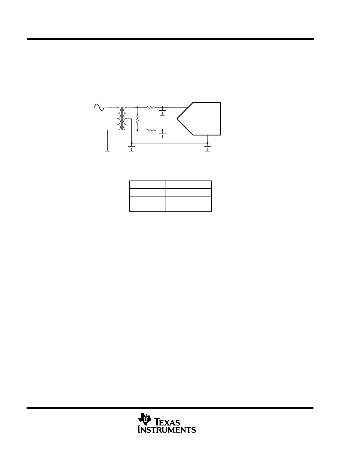
AC-coupled single-ended configuration
If the application does not require the signal bandwidth to include dc, the level shift shown in Figure 4 is not
necessary.
10 kΩ
10 kΩ
REF+
10 kΩ 10 kΩ
–
+
100 pF
10 nF
22 Ω
100 pF
Figure 22. Single-Ended With Level Shift
IN+
THS1401/3/8
IN–
10 kΩ
10 kΩ
REF–
Because the signal swing on the op-amp is centered around ground, it is more likely that the signal stays within the
linear region of the op-amp transfer function, thus increasing the overall ac performance.
IN [V
–∆REF – full scale
] OUTPUT [
PEAK
0 0
∆REF + full scale
PEAK
]
Compared to the transformer-coupled configuration, the swing on IN– is twice as big, which can decrease the ac
performance (SNR, SFD, and THD).
20
POST OFFICE BOX 655303 • DALLAS, TEXAS 75265

THS1401-EP THS1403-EP THS1408-EP
14-BIT, 1/3/8 MSPS DSP COMPATIBLE ANALOG-TO-DIGITAL CONVERTERS
WITH INTERNAL REFERENCE AND PGA
SGLS129A – JULY 2002 – REVISED NOVEMBER 2002
APPLICATION INFORMATION
internal/external reference operation
The THS1401/3/8 ADC can either be operated using the built-in band gap reference or using an external precision
reference in case very high dc accuracy is needed.
The REF+ and REF+ outputs are given by:
REF
)+
If the built-in reference is used, VBG equals 1.5 V which results in REF+ = 2.5 V, REF– = 0.5 V and ∆REF = 2 V.
The internal reference can be disabled by writing 1 to D12 (REF) in the control register (address 3). The band gap
reference is then disconnected and can be substituted by a voltage on the VBG pin.
VBG
ǒ
Ǔ
1
)
and REF–+VBGǒ1–
3
2
2
Ǔ
3
programmable gain amplifier
The on-chip programmable gain amplifier (PGA) has eight gain settings. The gain can be changed by writing to the
PGA gain register (address 1). The range is 0 to 7dB in steps of one dB.
out of range indication
The OV output of the ADC indicates an out of range condition. Every time the difference on the analog inputs
exceeds the differential reference, this signal is asserted. This signal is updated the same way as the digital data
outputs and therefore subject to the same pipeline delay.
offset compensation
With the offset register it is possible to automatically compensate system offset errors, including errors caused by
additional signal conditioning circuitry. If the offset compensation is enabled (D7 (OFF) in the control register), the
value in the offset register (address 2) is automatically subtracted from the output of the ADC.
In order to set the correct value of the offset compensation register , the ADC result when the input signal is 0 must
be read by the host processor and written to the offset register (address 2).
test modes
The ADC core operation can be tested by selecting one of the available test modes (see control register description).
The test modes apply various voltages to the differential input depending on the setting in the control register.
digital I/O
The digital inputs and outputs of the THS1401/3/8 ADC are 3-V CMOS compatible. In order to avoid current feed
back errors, the capacitive load on the digital outputs should be as low as possible (50 pF max). Series resistors
(100 Ω) on the digital outputs can improve the performance by limiting the current during output transitions.
The parallel interface of the THS1401/3/8 ADC features 3-state buffers, making it possible to directly connect it to
a data bus. The output buffers are enabled by driving the OE
Refer to the read and write timing diagrams in the parameter measurement information section for information on
read and write access.
POST OFFICE BOX 655303 • DALLAS, TEXAS 75265
input low.
21

THS1401-EP THS1403-EP THS1408-EP
14-BIT, 1/3/8 MSPS DSP COMPATIBLE ANALOG-TO-DIGITAL CONVERTERS
WITH INTERNAL REFERENCE AND PGA
SGLS129A – JULY 2002 – REVISED NOVEMBER 2002
MECHANICAL DATA
PHP (S-PQFP-G48) PowerPAD PLASTIC QUAD FLATPACK
37
48
1,05
0,95
0,50
36
0,27
0,17
25
24
13
1
5,50 TYP
7,20
SQ
6,80
9,20
SQ
8,80
12
M
0,08
Seating Plane
Thermal Pad
(see Note D)
0,15
0,05
0,13 NOM
Gage Plane
0,25
0°–7°
0,75
0,45
1,20 MAX
NOTES: A. All linear dimensions are in millimeters.
B. This drawing is subject to change without notice.
C. Body dimensions do not include mold flash or protrusion.
D. The package thermal performance may be enhanced by bonding the thermal pad to an external thermal plane.
This pad is electrically and thermally connected to the backside of the die and possibly selected leads.
E. Falls within JEDEC MS-026
PowerPAD is a trademark of Texas Instruments.
0,08
4146927/A 01/98
22
POST OFFICE BOX 655303 • DALLAS, TEXAS 75265

IMPORTANT NOTICE
Texas Instruments Incorporated and its subsidiaries (TI) reserve the right to make corrections, modifications,
enhancements, improvements, and other changes to its products and services at any time and to discontinue
any product or service without notice. Customers should obtain the latest relevant information before placing
orders and should verify that such information is current and complete. All products are sold subject to TI’s terms
and conditions of sale supplied at the time of order acknowledgment.
TI warrants performance of its hardware products to the specifications applicable at the time of sale in
accordance with TI’s standard warranty . Testing and other quality control techniques are used to the extent TI
deems necessary to support this warranty . Except where mandated by government requirements, testing of all
parameters of each product is not necessarily performed.
TI assumes no liability for applications assistance or customer product design. Customers are responsible for
their products and applications using TI components. T o minimize the risks associated with customer products
and applications, customers should provide adequate design and operating safeguards.
TI does not warrant or represent that any license, either express or implied, is granted under any TI patent right,
copyright, mask work right, or other TI intellectual property right relating to any combination, machine, or process
in which TI products or services are used. Information published by TI regarding third–party products or services
does not constitute a license from TI to use such products or services or a warranty or endorsement thereof.
Use of such information may require a license from a third party under the patents or other intellectual property
of the third party , or a license from TI under the patents or other intellectual property of TI.
Reproduction of information in TI data books or data sheets is permissible only if reproduction is without
alteration and is accompanied by all associated warranties, conditions, limitations, and notices. Reproduction
of this information with alteration is an unfair and deceptive business practice. TI is not responsible or liable for
such altered documentation.
Resale of TI products or services with statements different from or beyond the parameters stated by TI for that
product or service voids all express and any implied warranties for the associated TI product or service and
is an unfair and deceptive business practice. TI is not responsible or liable for any such statements.
Mailing Address:
Texas Instruments
Post Office Box 655303
Dallas, Texas 75265
Copyright 2002, Texas Instruments Incorporated
 Loading...