

T
查询THS1215供应商
THS1215
3.3-V, 12-BIT, 15 MSPS, LOW-POWER ANALOG-TO-DIGITAL CONVERTER
WITH POWER DOWN
SLAS292 – MARCH 2001
features
D
Configurable Input Functions:
– Single-Ended
– Single-Ended With Offset
– Differential
D
3.3-V Supply Operation
D
Internal Voltage Reference
D
Out-of-Range Indicator
D
Power-Down Mode
applications
D
Camcorders
D
Digital Cameras
D
Copiers
D
Communications
D
Test Instruments
D
Baseband Digitization
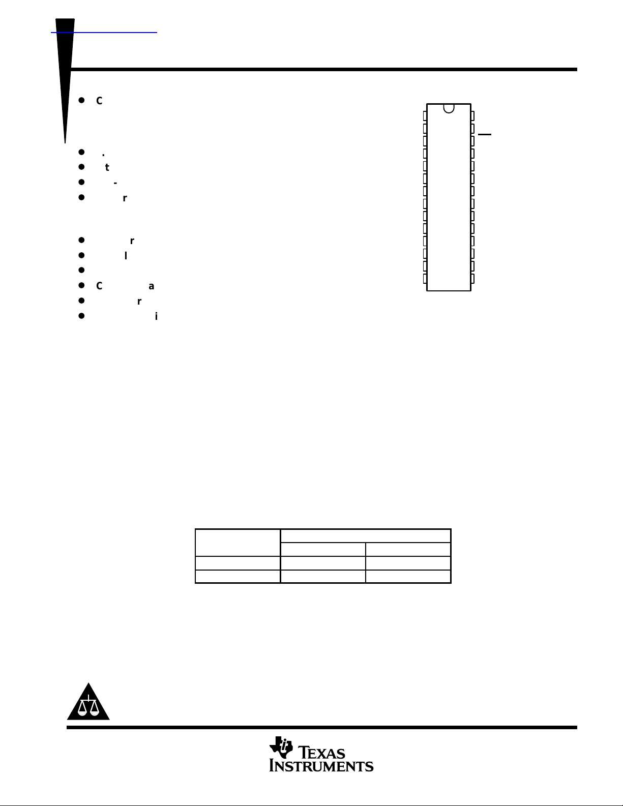
DW OR PW PACKAGE
(TOP VIEW)
AGND
CON1
CON0
EXTREF
AIN+
AIN–
AGND
AV
REFT
REFB
OVRNG
DD
D11
D10
D9
1
2
3
4
5
6
7
8
9
10
11
12
13
14
28
27
26
25
24
23
22
21
20
19
18
17
16
15
CLK
AV
DD
OE
D0
D1
D2
D3
D4
DV
DD
DGND
D5
D6
D7
D8
description
The THS1215 is a CMOS, low power, 12-bit, 15 MSPS analog-to-digital converter (ADC) that operates with a
3.3-V supply . The THS1215 gives circuit developers complete flexibility . The analog input to the THS1215 can
be either single-ended, single-ended with offset, or differential. The THS1215 provides a wide selection of
voltage references to match the user’s design requirements. For more design flexibility, the internal reference
can be bypassed to use an external reference to suit the dc accuracy and temperature drift requirements of the
application. The out-of-range output is used to monitor any out-of-range condition in the THS1215’s input range.
The speed, resolution, and single-supply operation of the THS1215 are suited for applications in video,
multimedia, high-speed acquisition, and communications. The speed and resolution ideally suit charge-couple
device (CCD) input systems such as digital copiers, digital cameras, and camcorders. The wide input voltage
range between V
REFB
and V
allows the THS1215 to be designed into multiple systems.
REFT
The THS1215C is characterized for operation from 0°C to 70°C. The THS1215I is characterized for operation
from –40°C to 85°C.
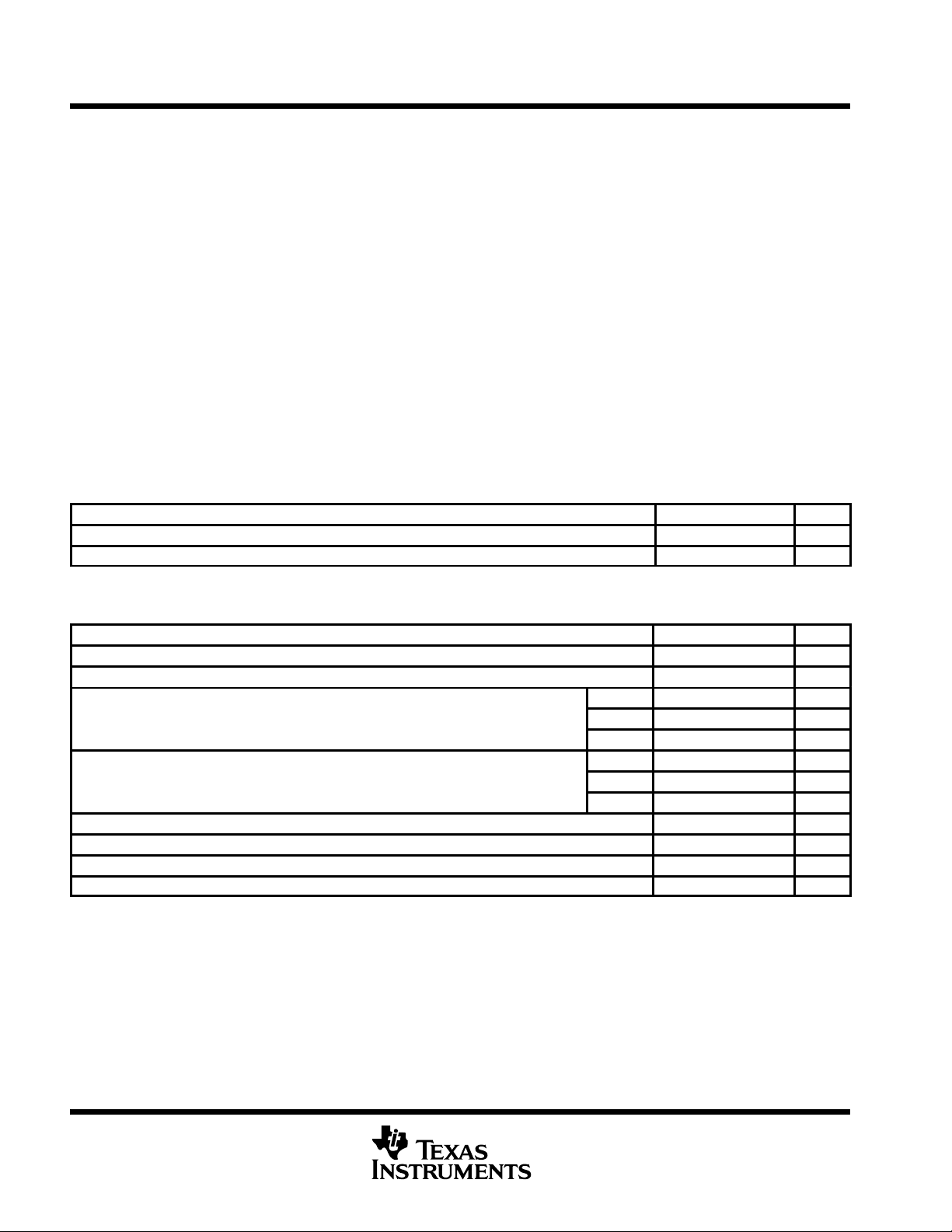
AVAILABLE OPTIONS
A
0°C to 70°C THS1215CPW THS1215CDW
–40°C to 85°C THS1215IPW THS1215IDW
Please be aware that an important notice concerning availability, standard warranty, and use in critical applications of
Texas Instruments semiconductor products and disclaimers thereto appears at the end of this data sheet.
28-TSSOP (PW) 28-SOIC (DW)
PACKAGED DEVICES
PRODUCTION DATA information is current as of publication date.
Products conform to specifications per the terms of Texas Instruments
standard warranty. Production processing does not necessarily include
testing of all parameters.
POST OFFICE BOX 655303 • DALLAS, TEXAS 75265
Copyright 2001, Texas Instruments Incorporated
1
THS1215
3.3-V, 12-BIT, 15 MSPS, LOW-POWER ANALOG-TO-DIGITAL CONVERTER
WITH POWER DOWN
SLAS292 – MARCH 2001
functional block diagram
DV
DD
CLK
AIN+
AIN–
CON0
CON1
Sample
and Hold
Configuration
Control
Circuit
Internal
Reference
Circuit
Timing Circuitry
12-Bit ADC
EXTREF
REFT
REFB
AV
DD
3-State
Output
Buffers
DGNDAGND
OVRNG
D[11:0]
OE
2
POST OFFICE BOX 655303 • DALLAS, TEXAS 75265

I/O
DESCRIPTION
3.3-V, 12-BIT, 15 MSPS, LOW-POWER ANALOG-TO-DIGITAL CONVERTER
Terminal Functions
TERMINAL
NAME NO.
AGND 1, 7 I Analog ground
AV
DD
AIN+ 5 I Positive analog input
AIN– 6 I Negative analog input
CLK 28 I ADC conversion clock
CON1 2 I Configuration Input 1
CON0 3 I Configuration Input 0
DGND 19 I Digital ground
DV
DD
D11 12 O ADC data bit 11
D10 13 O ADC data bit 10
D9 14 O ADC data bit 9
D8 15 O ADC data bit 8
D7 16 O ADC data bit 7
D6 17 O ADC data bit 6
D5 18 O ADC data bit 5
D4 21 O ADC data bit 4
D3 22 O ADC data bit 3
D2 23 O ADC data bit 2
D1 24 O ADC data bit 1
D0 25 O ADC data bit 0
EXTREF 4 I Reference select input, high = external, low = internal
OVRNG 11 O Out of range indicator
OE 26 I Output enable, high = disable, low = enable
REFT 9 I/O Upper ADC reference voltage
REFB 10 I/O Lower ADC reference voltage
8, 27 I Analog supply
20 I Digital supply
THS1215
WITH POWER DOWN
SLAS292 – MARCH 2001
POST OFFICE BOX 655303 • DALLAS, TEXAS 75265
3
THS1215
3.3-V, 12-BIT, 15 MSPS, LOW-POWER ANALOG-TO-DIGITAL CONVERTER
WITH POWER DOWN
SLAS292 – MARCH 2001
absolute maximum ratings over operating free-air temperature (unless otherwise noted)
Supply voltage range: AV
to AGND, DVDD to DGND –0.3 to 4 V. . . . . . . . . . . . . . . . . . . . . . . . . . . . . . . . .
DD
†
AGND to DGND –0.3 to 0.3 V. . . . . . . . . . . . . . . . . . . . . . . . . . . . . . . . . . . . . . . . . . . . . .
Reference voltage input range, REFT, REFB to AGND –0.3 to AV
Analog input voltage range, AIN+, AIN– to AGND –0.3 to AV
Clock input voltage range, CLK to AGND –0.3 to AV
Digital input voltage range, digital input to DGND –0.3 to DV
Digital output voltage range, digital output to DGND –0.3 to DV
Operating junction temperature range, T
Storage temperature range, T
–65°C to 150°C. . . . . . . . . . . . . . . . . . . . . . . . . . . . . . . . . . . . . . . . . . . . . . . . .
STG
–40°C to 150°C. . . . . . . . . . . . . . . . . . . . . . . . . . . . . . . . . . . . . . . . . . .
J
DD
DD
DD
DD
DD
+ 0.3 V. . . . . . . . . . . . . . . . . . . . . . . . . . .
+ 0.3 V. . . . . . . . . . . . . . . . . . . . . . . . . . . . . . .
+ 0.3 V. . . . . . . . . . . . . . . . . . . . . . . . . . . . . . . . . . . . . .
+ 0.3 V. . . . . . . . . . . . . . . . . . . . . . . . . . . . . . . .
+ 0.3 V. . . . . . . . . . . . . . . . . . . . . . . . . . . . .
Lead temperature 1,6 mm (1/16 in) from case for 10 seconds 300°C. . . . . . . . . . . . . . . . . . . . . . . . . . . . . . . . . .
†
Stresses beyond those listed under “absolute maximum ratings” may cause permanent damage to the device. These are stress ratings only, and
functional operation of the device at these or any other conditions beyond those indicated under “recommended operating conditions” is not
implied. Exposure to absolute-maximum-rated conditions for extended periods may affect device reliability.
electrical characteristics over recommended operating conditions (AVDD = DVDD = 3.3 V,
= 15 MHz/50% duty cycle, MODE = 1, 1-V input span, internal reference, T
f
s
min
to T
max
) ( unless
otherwise noted)
sampling rate and resolution
PARAMETER MIN NOM MAX UNIT
f
‡
Sample frequency 5
s
Resolution 12 Bits
The clock frequency may be extended to 5 MHz without degradation in specified performance.
‡
15 MSPS
analog inputs (all supplies = 3.3 V)
PARAMETER MIN TYP MAX UNIT
Positive analog input, AIN+ 0 AV
Negative analog input, AIN– 0 AV
MODE1 –1 V
Analog input voltage difference for zero scale ADC out, (AIN+) – (AIN–)
Analog input voltage difference for full scale ADC out, (AIN+) – (AIN–)
Switched input capacitance, C
Aperture delay time, t
Aperture uncertainty (jitter) 2 ps
DC leakage current (input = ±FS) 10 µA
d(ap)
i
MODE2 –2 V
MODE3 0 V
MODE1 1 V
MODE2 2 V
MODE3 1 V
DD
DD
6 pF
2 ns
V
V
4
POST OFFICE BOX 655303 • DALLAS, TEXAS 75265
VIHHigh level input voltage
VILLow level input voltage
THS1215
3.3-V, 12-BIT, 15 MSPS, LOW-POWER ANALOG-TO-DIGITAL CONVERTER
WITH POWER DOWN
SLAS292 – MARCH 2001
electrical characteristics over recommended operating conditions (AVDD = DVDD = 3.3 V,
= 15 MHz/50% duty cycle, MODE = 1, 1-V input span, internal reference, T
f
s
otherwise noted) (continued)
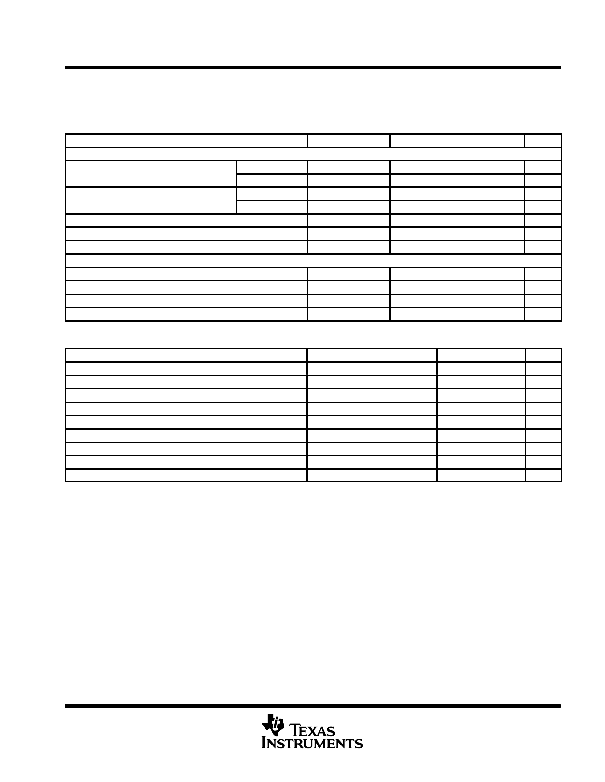
digital inputs and outputs (all supplies = 3.3 V)
PARAMETER TEST CONDITION MIN TYP MAX UNIT
Digital Inputs
p
p
I
High level input current 1 µA
IH
I
Low level input current –1 µA
IL
C
Input capacitance 5 pF
i
Digital Outputs
V
High level output voltage I
OH
V
Low level output voltage I
OL
High impedance output current ±1 µA
tr/t
Rise/fall time CL = 10 pF 5.5 ns
f
All other inputs 0.8 × DV
CLK 0.8 × AV
All other inputs 0.2 × DV
CLK 0.2 × AV
= 50 µA DVDD–0.4 V
load
= –50 µA 0.4 V
load
DD
DD
min
to T
max
DD
DD
) (unless
V
V
power supply (CLK = 15 MHz)
PARAMETER TEST CONDITION MIN TYP MAX UNIT
XV
DD
I
DD
I
(analog)
I
(digital)
I
I(standby)
t
(PU)
P
D
P
D(STBY)
PSRR Power supply rejection ratio ±0.1 %FS
Supply voltage (all supplies) 3 3.3 3.6 V
Supply current active – total 45 53.5 mA
Supply current active – analog 34 mA
Supply current active – digital 11 mA
Standby supply current CLK = 0 MHz 10 µA
Power-up time for references from standby 100 µs
Power dissipation CLK = 15 MHz 148 177 mW
Standby power dissipation CLK = 0 MHz 36 µW
POST OFFICE BOX 655303 • DALLAS, TEXAS 75265
5
THS1215
3.3-V, 12-BIT, 15 MSPS, LOW-POWER ANALOG-TO-DIGITAL CONVERTER
WITH POWER DOWN
SLAS292 – MARCH 2001
electrical characteristics over recommended operating conditions (AVDD = DVDD = 3.3 V,
= 15 MHz/50% duty cycle, MODE = 1, 1-V input span, internal reference, T
f
s
otherwise noted) (continued)
REFT, REFB reference voltages (all supplies = 3.3 V)
PARAMETER TEST CONDITION MIN TYP MAX UNIT
Internal Reference
V
REFT
V
REFB
V
REF
External Reference
Internal or External Reference
C
T
C
B
C
TB
Upper reference voltage 2.15 V
Lower reference voltage 1.15 V
Differential reference voltage, V
Differential reference voltage, V
Externally applied V
Externally applied V
Externally applied (V
External mode V
V
decoupling capacitor value 0.1 µF
REFT
V
decoupling capacitor value 0.1 µF
REFB
Decoupling capacitor V
REFT
REFB
REFT–VREFB
to V
REFT
REFT–VREFB
REFT–VREFB
reference voltage range 2 2.5 V
reference voltage range 1.05 1.3 V
) reference voltage range 0.75 1.05 V
impedance 9 kΩ
REFB
to V
REFT
REFB
accuracy –5% 5%
to T
min
0.95 1 1.05 V
10 µF
max
) (unless
dc accuracy (linearity)
PARAMETER TEST CONDITIONS MIN TYP MAX UNIT
Number of missing codes All modes 0 codes
DNL Differential nonlinearity All modes ±0.43 ±0.9 LSB
INL Integral nonlinearity All modes ±0.6 ±1.5 LSB
Offset error All modes 0.5 1.2 %FSR
Gain error All modes 0.5 3.5 %FSR
dynamic performance (all supplies = 3.3 V)
PARAMETER TEST CONDITIONS MIN TYP MAX UNIT
ENOB Effective number of bits fi = 3.58 MHz 10.7 11.1 Bits
THD Total harmonic distortion fi = 3.58 MHz –81.2 dB
SNR Signal-to-noise ratio fi = 3.58 MHz 67.4 68.9 dB
SINAD Signal-to-noise + distortion fi = 3.58 MHz 66 68.6 dB
SFDR Spurious free dynamic range fi = 3.58 MHz 72 81.7 dB
Analog input bandwidth 180 MHz
Differential phase, DP 0.12 degree
G
Differential gain 0.01%
(diff)
timing (all supplies = 3.3 V)
PARAMETER TEST CONDITION MIN TYP MAX UNIT
f
CLK
t
d(O)
t
d(PZ)
t
d(EN)
†
The clock frequency may be extended down to 5 MHz without degradation in specified performance.
Clock frequency
Clock duty cycle 45% 50% 55%
Output delay time 19 ns
Delay time, output disable to Hi-Z output 3.2 ns
Delay time, output enable to output valid 16 19 ns
Latency 5 cycles
†
5 15 MHz
6
POST OFFICE BOX 655303 • DALLAS, TEXAS 75265
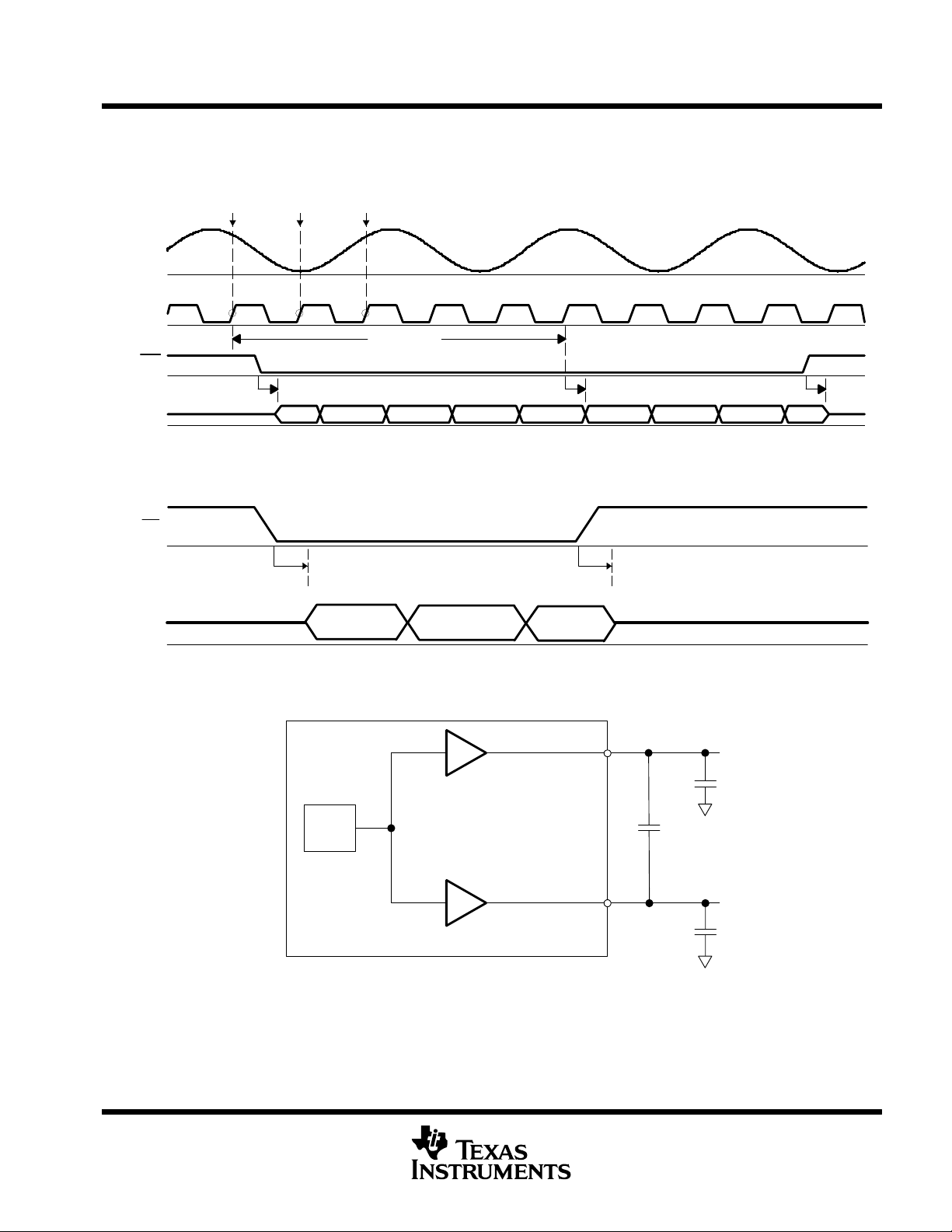
timing diagram
THS1215
3.3-V, 12-BIT, 15 MSPS, LOW-POWER ANALOG-TO-DIGITAL CONVERTER
WITH POWER DOWN
SLAS292 – MARCH 2001
PARAMETER MEASUREMENT INFORMATION
Analog
CLK
OE
D[9:0]
OE
D[9:0]
S1
123456789
S2 S3
t
d(EN)
t
PIPELINE
t
d(O)
S1 S2 S3
Figure 1. Input Timing
t
d(EN)
Hi–Z Hi–Z
Data Data Data
t
d(PZ)
10
t
d(PZ)
THS1215
1.5 V
BAND
GAP
Figure 2. Output Timing
Figure 3. Reference Generation
REFT
C
T
C
TB
REFB
C
B
POST OFFICE BOX 655303 • DALLAS, TEXAS 75265
7

THS1215
3.3-V, 12-BIT, 15 MSPS, LOW-POWER ANALOG-TO-DIGITAL CONVERTER
WITH POWER DOWN
SLAS292 – MARCH 2001
TYPICAL CHARACTERISTICS
POWER
vs
TEMPERATURE
Power – mW
152
151
150
149
148
147
146
145
144
fs = 15 MSPS
–40 –15 10 35 60 85
TA – Temperature – °C
Figure 4
SIGNAL-TO-NOISE
vs
TEMPERATURE
71
AVDD = DVDD = 3.3 V,
fIN = 3.58 MHz,
fs = 15 MSPS,
70
Mode = 1
69
68
SNR – Signal-to-Noise – dB
67
66
–40 –15 10 35 60 85
TA – Temperature – °C
Figure 5
SPURIOUS FREE DYNAMIC RANGE
vs
TEMPERATURE
84
82
80
78
76
74
AVDD = DVDD = 3.3 V,
72
SFDR – Spurious Free Dynamic Range – dB
fIN = 3.58 MHz,
fs = 15 MSPS
70
–40 –15 10 35 60 85
TA – Temperature – °C
Figure 6
TOTAL HARMONIC DISTORTION
vs
TEMPERATURE
–78
AVDD = DVDD = 3.3 V,
fIN = 3.58 MHz,
fs = 15 MSPS
–80
–82
–84
–86
THD – Total Harmonic Distortion – dB
–88
–40 –15 10 35 60 85
TA – Temperature – °C
Figure 7
8
POST OFFICE BOX 655303 • DALLAS, TEXAS 75265

THS1215
3.3-V, 12-BIT, 15 MSPS, LOW-POWER ANALOG-TO-DIGITAL CONVERTER
WITH POWER DOWN
SLAS292 – MARCH 2001
TYPICAL CHARACTERISTICS
SIGNAL-TO-NOISE AND DISTORTION
vs
TEMPERATURE
69.0
68.5
68.0
67.5
67.0
DNL – Differential Nonlinearity – LSB
66.5
SINAD – Signal-to-Noise and Distortion – dB
AVDD = DVDD = 3.3 V,
fIN = 3.58 MHz,
fs = 15 MSPS
66
–40 –15 10 35 60 85
TA – Temperature – °C
Figure 8
DIFFERENTIAL NONLINEARITY (DNL)
1.00
0.80
0.60
0.40
0.20
–0.00
–0.20
–0.40
–0.60
–0.80
–1.00
0 512 1024 1536 2048 2560 3072 3584 4096
ADC Code
AVDD = 3.3 V,
DVDD = 3.3 V,
fs = 15 MSPS
Figure 9
POST OFFICE BOX 655303 • DALLAS, TEXAS 75265
9
THS1215
3.3-V, 12-BIT, 15 MSPS, LOW-POWER ANALOG-TO-DIGITAL CONVERTER
WITH POWER DOWN
SLAS292 – MARCH 2001
TYPICAL CHARACTERISTICS
INTEGRAL NONLINEARITY (INL)
1.5
1.0
0.5
0.0
–0.5
AVDD = 3.3 V,
DVDD = 3.3 V,
fs = 15 MSPS
INL – Integral Nonlinearity – LSB
Power – dBFS
–1.0
–1.5
0 512 1024 1536 2048 2560 3072 3584 4096
ADC Code
Figure 10
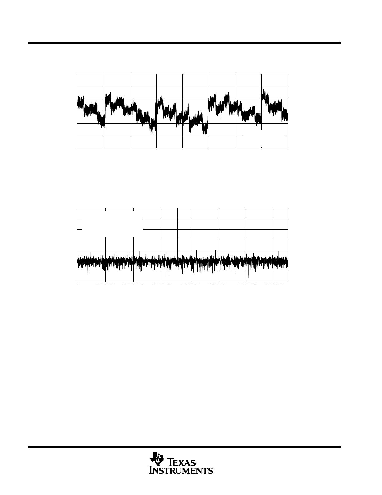
FFT
vs
FREQUENCY
0
–20
–40
–60
–80
–100
–120
–140
AVDD = DVDD = 3.3 V,
fIN = 3.5 MHz
fs = 15 MSPS,
Mode = 1
0 1000000 2000000 3000000 4000000 5000000 6000000 7000000
01234567
f – Frequency – MHz
Figure 11
10
POST OFFICE BOX 655303 • DALLAS, TEXAS 75265

THS1215
3.3-V, 12-BIT, 15 MSPS, LOW-POWER ANALOG-TO-DIGITAL CONVERTER
WITH POWER DOWN
SLAS292 – MARCH 2001
TYPICAL CHARACTERISTICS
BANDWIDTH
3
0
–3
–6
–9
Amplitude – dB
–12
AVDD = DVDD = 3.3 V,
–15
fIN = 3.58 MHz,
fs = 15 MSPS
–18
2 20 200
f – Frequency – MHz
Figure 12
POST OFFICE BOX 655303 • DALLAS, TEXAS 75265
11

THS1215
3.3-V, 12-BIT, 15 MSPS, LOW-POWER ANALOG-TO-DIGITAL CONVERTER
WITH POWER DOWN
SLAS292 – MARCH 2001
PRINCIPLES OF OPERATION
analog input
The analog input AIN is sampled in the sample and hold unit, the output of which feeds the ADC CORE, where
the process of analog to digital conversion is performed against ADC reference voltages, V
Connecting the EXTREF pin to one of two voltages, DGND or DV
selects one of the two configurations of
DD
ADC reference generation. The ADC reference voltages come from either the internal reference buffer or
completely external sources. Connect EXTREF to DGND for internal reference generation or to DV
external reference generation.
CON0 and CON1 as described below, select the input configuration mode or place the device in powerdown.
The ADC core drives out through output buffers to the data pins D0 to D1 1. The output buffers can be disabled
by the OE
pin.
A single, sample-rate clock (15 MHz maximum) is required at pin CLK. The analog input signal is sampled on
the rising edge of CLK, and corresponding data is output after the fifth following rising edge.
The THS1215 can operate in four input modes, controlled by the configuration pins CON0 and CON1 as shown
in Table 1.
REFT
and V
REFB
for
DD
.
Table 1. Input Modes of Operation
MODE CON1 CON0 MODE OF OPERATION
0 0 0 Device powered down
1 0 1 Single-ended mode/differential mode × 1
2 1 0 Differential mode ×0.5
3 1 1 Single-ended mode with of fset
12
POST OFFICE BOX 655303 • DALLAS, TEXAS 75265

3.3-V, 12-BIT, 15 MSPS, LOW-POWER ANALOG-TO-DIGITAL CONVERTER
analog input (continued)
Modes 1, 2, and 3 are shown in Figure 13.
THS1215
WITH POWER DOWN
SLAS292 – MARCH 2001
PRINCIPLES OF OPERATION
4095
AIN–
AIN+
MODE 1, CON[1:0] = 01
AIN–
AIN+
MODE2, CON[1:0] = 10
AIN+
AIN–
1V
1V
0
4095
2V
0
4095
1V
0
AIN–
AIN+
OUTPUT CODEOUTPUT CODE
MODE 1, CON[1:0] = 01
AIN+
CODE
OUTPUT
AIN–
1V
1V
4095
OUTPUT
0
0
OUTPUT
4095
CODE
CODE
MODE3, CON[1:0] = 11
MODE3, CON[1:0] = 11
Figure 13. Input Mode Configurations
The difference between the AIN– and the AIN+ inputs is different in all three cases. The THS1215 automatically
switches gain and offset in the S/H to accommodate for the input signals. This automatic switching is covered
in Table 2.
Table 2. Input Mode Switching
MODE CON1 CON0
1 0 1 –1 V 1 V ×1 0 V
2 1 0 –2 V 2 V ×0.5 0 V
3 1 1 0 V 1 V ×1 –1 V
(AIN+) – (AIN–)
MIN
POST OFFICE BOX 655303 • DALLAS, TEXAS 75265
(AIN+) – (AIN–)
MAX
S/H GAIN S/H OFFSET
13

THS1215
3.3-V, 12-BIT, 15 MSPS, LOW-POWER ANALOG-TO-DIGITAL CONVERTER
WITH POWER DOWN
SLAS292 – MARCH 2001
PRINCIPLES OF OPERATION
analog input (continued)
Table 2 assumes that the delta in ADC reference voltages V
V
REFT
– V
= 1 V . Note that V
REFB
REFB
and V
can be set externally , which will scale the numbers given in
REFT
REFT
and V
is set to 1 V, i.e.,
REFB
this table.
The user-chosen operating configuration and reference voltages determine what input signal voltage range the
THS1215 can handle.
The following sections explain both the internal signal flow of the device and how the input signal span is related
to the ADC reference voltages, as well as the ways in which the ADC reference voltages can be buffered
internally or externally applied.
signal processing chain (sample and hold, ADC)
Figure 14 shows the signal flow through the sample and hold unit and the PGA to the ADC core.
REFT
AIN+
AIN–
+1
–1
SAMPLE
AND
HOLD
Figure 14. Analog Input Signal Flow
VP+
ADC
CORE
VP–
REFB
sample and hold
The differential sample and hold processes AIN with respect to the voltages applied to the REFT and REFB pins,
to give a differential output (VP+) – (VP–) = VP given by:
VP = (AIN+) – ( AIN–)
For single-ended input signals, AIN– is a constant voltage; usually the AIN midscale input voltage. However if
MODE = 3 (see Table 1) then AIN– or AIN+ can be used to create an offset for the other input in single-ended
mode.
14
POST OFFICE BOX 655303 • DALLAS, TEXAS 75265

3.3-V, 12-BIT, 15 MSPS, LOW-POWER ANALOG-TO-DIGITAL CONVERTER
analog-to-digital converter
THS1215
WITH POWER DOWN
SLAS292 – MARCH 2001
PRINCIPLES OF OPERATION
No matter what operating configuration is chosen, VP is digitized against ADC reference voltages V
V
at AIN greater than REFTS or less than V
REFB
. The V
REFT
and V
voltages set the analog input span limits FS+ and FS– respectively . Any voltages
REFB
REFBS
will cause ADC over-range, which is signaled by OVR going
high when the conversion result is output.
analog input
A first-order approximation for the equivalent analog input circuit of the THS1215 is shown in Figure 15. The
equivalent input capacitance C
is 5 pF typical. The input must charge/discharge this capacitance within the
I
sample period of one half of a clock cycle. When a full-scale voltage step is applied, the input source provides
the charging current through the switch resistance R
(200 Ω) of S1 and quickly settles. In this case the input
SW
impedance is low. Alternatively, when the source voltage equals the value previously stored on C
capacitor requires no input current and the equivalent input impedance is very high.
THS1215
R
R
VS+V
+
V
CM
_
–
S
R
S
S
SW
R
SW
C
I
V
CM
C
I
+
_
and
REFT
, the hold
I
Figure 15. Simplified Equivalent Input Circuit
To maintain the frequency performance outlined in the specifications, the total source impedance should be
limited to the following equation with f
RSt
2f
CLK
1
CI
In(256)
–R
SW
So, for applications running at a lower f
= 15 MHz, CI = 5 pF, RSW = 200 Ω:
CLK
, the total source resistance can increase proportionally.
CLK
The analog input of the THS1215 is a differential input that can be configured in various ways depending on
the signal source and the required level of performance. A fully differential connection (see Figure 16) will deliver
the best performance from the converter.
POST OFFICE BOX 655303 • DALLAS, TEXAS 75265
15

THS1215
3.3-V, 12-BIT, 15 MSPS, LOW-POWER ANALOG-TO-DIGITAL CONVERTER
WITH POWER DOWN
SLAS292 – MARCH 2001
PRINCIPLES OF OPERATION
analog input (continued)
AV
DD
2
R2
THS1215
AIN+
V
IN+
C1
R1
–
+
R2
–
+
AIN–
REFT
REFB
V
IN–
C2
C1
C2
R1
Figure 16. AC-Coupled Differential Input
The analog input can be dc-coupled (see Figure 17) as long as the inputs are within the analog input common
mode voltage range. For example (see Figure 17), V
peak-to-peak voltage of 2 V , and the circuit in Figure 17 is used to interface it with the THS1215. Assume A V
IN+
and V
are signals centered on GND with a
IN–
DD
of the converter is 3 V. Two problems have to be solved. The first is to shift CML from 0 V to 1.5 V (AVDD/2).
To do that, a V bias voltage and an adequate ratio of R1 and R2 have to be selected. For instance, if V
bias = A V
= 3 V , then R1 = R2. The second is that the dif ferential voltage has to be reduced from 4 V (2 x 2
DD
V) to 1 V, and for that an attenuation of 4 to1 is needed. The attenuation is determined by the relation:
(R3||2R2)/((R3||2R2) + 2R1). One possible solution is R1 = R2 = R3 = 150 Ω. In this case, moreover, the input
impedance (2R1 + (R3||2R2)) will be 400 Ω. The values can be changed to match any other input impedance.
A capacitor, C, connected from AIN+ to AIN– will help filter any high frequency noise on the inputs, also
improving performance. Note that the chosen value of capacitor C must take into account the highest frequency
component of the analog input signal.
16
POST OFFICE BOX 655303 • DALLAS, TEXAS 75265

3.3-V, 12-BIT, 15 MSPS, LOW-POWER ANALOG-TO-DIGITAL CONVERTER
analog input (continued)
V
IN+
V
IN–
R1
R1
V
BIAS
V
BIAS
THS1215
WITH POWER DOWN
SLAS292 – MARCH 2001
PRINCIPLES OF OPERATION
THS1215
R2
AIN+
R3
AIN–
R2
REFT
REFB
Figure 17. DC-Coupled Differential Input Circuit
The configuration shown in Figure 18 may be used with a single-ended ac-coupled input. If V
is a 1 V
IN
PP
sinewave, then AIN+ is a 1 VPP sinewave riding on a positive voltage equal to AVDD/2. The converter will be
at positive full scale when AIN+ is at AV
AV
/2 – 0.5 V. Sufficient headroom must be provided such that the input voltage never goes above 3.3 V or
DD
/2 + 0.5 V and will be at negative full scale when AIN+ is equal to
DD
below AGND.
A single-ended source may give better overall system performance if it is first converted to differential before
driving the THS1215.
AV
DD
2
THS1215
V
IN
AIN+
AIN–
REFT
REFB
Figure 18. Transformer Coupled Single-Ended Input
POST OFFICE BOX 655303 • DALLAS, TEXAS 75265
17

THS1215
3.3-V, 12-BIT, 15 MSPS, LOW-POWER ANALOG-TO-DIGITAL CONVERTER
WITH POWER DOWN
SLAS292 – MARCH 2001
PRINCIPLES OF OPERATION
digital outputs
The output of THS1215 is in unsigned binary code. The ADC input over-range indicator is output on pin OVRNG.
Capacitive loading on the output should be kept as low as possible (a maximum loading of 10 pF is
recommended) to ensure best performance. Higher output loading causes higher dynamic output currents and
can therefore increase noise coupling into the part’s analog front end. T o drive higher loads the use of an output
buffer is recommended.
When clocking output data from THS1215, it is important to observe its timing relation to CLK. The pipeline ADC
delay is 5 clock cycles to which the maximum output propagation delay needs to be added.
THS1215
DA11
DA0
CLK
SN74ALVCH16841
12
1D9
1D0
2D1
2D0
2D7
2D2
LE
OE
1Q9
1Q0
2Q1
2Q0
2Q9
2Q2
Figure 19. Buffered Output Connection
THS1215
DA11
DA0
12
D11
D0
D15
D12
WRTCLK
12
FIFO
1Q15
1Q0
16
HF flag INTR
ASIC
or
DSP
DSP
15 MHz
Clock
Figure 20. FIFO Connection
layout, decoupling and grounding rules
Proper grounding and layout of the PCB on which THS1215 is populated is essential to achieve the stated
performance. It is advised to use separate analog and digital ground planes that are spliced underneath the IC.
THS1215 has digital and analog pins on opposite sides of the package to make this easier. Since there is no
connection internally between analog and digital grounds, they have to be joined on the PCB. It is advised to
do this at one point in close proximity to THS1215.
Because of the high sampling rate and switched-capacitor architecture, THS1215 generates transients on the
supply and reference lines. Proper decoupling of these lines is therefore essential. EVM decoupling is
recommended as shown in Figure 21.
18
POST OFFICE BOX 655303 • DALLAS, TEXAS 75265

+3.3VD +3.3VD
+3.3VD +3.3VD
ADCDB[00:11]
LNK3
OEB
R2
47K
R1
47K
OEB
LNK2
CON1 CON0
CON1
+3.3VA+3.3VD
ADCDB00
ADCDB01
ADCDB02
ADCDB03
ADCDB04
ADCDB05
ADCDB06
ADCDB07
ADCDB08
ADCDB09
ADCDB10
ADCDB11
DACCLK
DACCLK
THS1215
3.3-V, 12-BIT, 15 MSPS, LOW-POWER ANALOG-TO-DIGITAL CONVERTER
WITH POWER DOWN
SLAS292 – MARCH 2001
PRINCIPLES OF OPERATION
+3.3VD +3.3VA
R23
47K
R24
47K
LNK4
EXTREF
LNK5
24
27
14
13
12
11
10
9
8
7
6
5
4
3
2
1
28
25
15
AVDD
DVDD
D0
D1
D2
D3
D4
D5
D6
D7
D8
D9
D10
D11
D12
D13
CLK
MODE
SLEEP
EXTREF
CON0
U3
THS5671AIPW
AGND
DGND
IOUT1
IOUT2
EXTLO
REFIO
FSADJ
COMP1
COMP2
+3.3VA
ADCCLK
ADCCLK
OEB
OEB
CON0
CON0
CON1
CON1
EXTREF
EXTREF
VINP
VINP
VINM
VINM
TP1 TP2
C28
C5
0.1uF
10uF
C25
0.1uF
+
C27
0.1uF
C26
0.1uF
+3.3VA
VRT
VRT
20
26
IOUT1
22
21
16
17
18
19
23
IOUT2
C6
0.1uF
IOUT1
IOUT2
C16
0.01uF
R10
2K
+3.3VA
C15
0.1uF
VRB
VRB
C19
+
10uF
C17
0.1uF
8
20
27
28
26
3
2
4
5
6
9
_3.3VA
+3.3VD
C18
0.1uF
U1
THS1215PW
AGND
AVDD
DGND
DVDD
AGND
CLKVDD
CLK
OE
CON0
CON1
EXTREF
AIN+
AIN–
D10
REFT
D11
REFB10OVRNG
C62
470pF
7
19
1
25
D0
24
D1
23
D2
22
D3
21
D4
18
D5
17
D6
16
D7
15
D8
14
D9
13
12
11
C63
0.1uF
ADCOVRNG
C64
470pF
ADCD00
ADCD01
ADCD02
ADCD03
ADCD04
ADCD05
ADCD06
ADCD07
ADCD08
ADCD09
ADCD10
ADCD11
C65
0.1uF
C66
470pF
ADCD [00:11]
+3.3VD
C67
0.1uF
Figure 21. EVM Schematic
definitions of specifications and terminology
integral nonlinearity (INL)
Integral nonlinearity refers to the deviation of each individual code from a line drawn from zero through full scale.
The point used as zero occurs 1/2 LSB before the first code transition. The full-scale point is defined as level
1/2 LSB beyond the last code transition. The deviation is measured from the center of each particular code to
the true straight line between these two end-points.
differential nonlinearity (DNL)
An ideal ADC exhibits code transitions that are exactly 1 LSB apart. DNL is the deviation from this ideal value.
Therefore, this measure indicates how uniform the transfer function step sizes are. The ideal step size is defined
here as the step size for the device under test, i.e. (last transition level – first transition level)/(2n –2). Using this
definition for DNL separates the effects of gain and offset error. A minimum DNL better than –1 LSB ensures
no missing codes.
POST OFFICE BOX 655303 • DALLAS, TEXAS 75265
19

THS1215
3.3-V, 12-BIT, 15 MSPS, LOW-POWER ANALOG-TO-DIGITAL CONVERTER
WITH POWER DOWN
SLAS292 – MARCH 2001
PRINCIPLES OF OPERATION
definitions of specifications and terminology (continued)
offset and gain error
Offset error (in LSBs) is defined as the average offset for all inputs, and gain error is defined as the maximum
error (in LSBs) caused by the angular deviation from the offset corrected straight line.
analog input bandwidth
The analog input bandwidth is defined as the maximum frequency of a 1 –dBFS input sine wave that can be
applied to the device for which an extra 3 –dB attenuation is observed in the reconstructed output signal.
output timing
Output timing td(O) is measured from the 50% level of the CLK input falling edge to the 10%/90% level of the
digital output. The digital output load is not higher than 10 pF.
Output hold time t
is measured from the 50% level of the CLK input falling edge to the10%/90% level of the
h(O)
digital output. The digital output load is not less than 2 pF.
Aperture delay t
is measured from the 50% level of the CLK input to the actual sampling instant.
d(A)
The OE signal is asynchronous.
OE timing t
is measured from the V
d(PZ)
IH(min)
level of OE to the high-impedance state of the output data. The
digital output load is not higher than 10 pF.
OE timing t
or V
OL(max)
is measured from the V
d(EN)
output levels. The digital output load is not higher than 10 pF.
level of OE to the instant when the output data reaches V
IL(max)
signal-to-noise ratio + distortion (SINAD)
SINAD is the ratio of the rms value of the measured input signal to the rms sum of all other spectral components
below the Nyquist frequency, including harmonics but excluding dc. The value for SINAD is expressed in
decibels.
effective number of bits (ENOB)
For a sine wave, SINAD can be expressed in terms of the number of bits. Using the following formula,
N = (SINAD – 1.76)/6.02
it is possible to get a measure of performance expressed as N, the effective number of bits. Thus, effective
number of bits for a device for sine wave inputs at a given input frequency can be calculated directly from its
measured SINAD.
total harmonic distortion (THD)
OH(min)
THD is the ratio of the rms sum of the first six harmonic components to the rms value of the measured input signal
and is expressed as a percentage or in decibels.
spurious free dynamic range (SFDR)
SFDR is the difference in dB between the rms amplitude of the input signal and the peak spurious signal.
20
POST OFFICE BOX 655303 • DALLAS, TEXAS 75265

THS1215
3.3-V, 12-BIT, 15 MSPS, LOW-POWER ANALOG-TO-DIGITAL CONVERTER
WITH POWER DOWN
SLAS292 – MARCH 2001
MECHANICAL DATA
DW (R-PDSO-G**) PLASTIC SMALL-OUTLINE PACKAGE
16 PINS SHOWN
0.050 (1,27)
16
1
0.020 (0,51)
0.014 (0,35)
9
0.299 (7,59)
0.291 (7,39)
8
A
0.010 (0,25)
0.419 (10,65)
0.400 (10,15)
M
0.010 (0,25) NOM
0°–8°
Gage Plane
0.010 (0,25)
0.050 (1,27)
0.016 (0,40)
0.104 (2,65) MAX
NOTES: A. All linear dimensions are in inches (millimeters).
B. This drawing is subject to change without notice.
C. Body dimensions do not include mold flash or protrusion not to exceed 0.006 (0,15).
D. Falls within JEDEC MS-013
0.012 (0,30)
0.004 (0,10)
DIM
A MAX
A MIN
PINS **
16
0.410
(10,41)
0.400
(10,16)
Seating Plane
0.004 (0,10)
20
0.510
(12,95)
0.500
(12,70)
0.610
(15,49)
0.600
(15,24)
24
28
0.710
(18,03)
0.700
(17,78)
4040000/D 01/00
POST OFFICE BOX 655303 • DALLAS, TEXAS 75265
21

THS1215
3.3-V, 12-BIT, 15 MSPS, LOW-POWER ANALOG-TO-DIGITAL CONVERTER
WITH POWER DOWN
SLAS292 – MARCH 2001
MECHANICAL DATA
PW (R-PDSO-G**) PLASTIC SMALL-OUTLINE PACKAGE
14 PINS SHOWN
0,65
1,20 MAX
14
0,30
0,19
8
4,50
4,30
PINS **
7
Seating Plane
0,15
0,05
8
1
A
DIM
14
0,10
6,60
6,20
M
0,10
0,15 NOM
0°–8°
2016
Gage Plane
24
0,25
0,75
0,50
28
A MAX
A MIN
NOTES: A. All linear dimensions are in millimeters.
B. This drawing is subject to change without notice.
C. Body dimensions do not include mold flash or protrusion not to exceed 0,15.
D. Falls within JEDEC MO-153
3,10
2,90
5,10
4,90
5,10
4,90
6,60
6,40
7,90
7,70
9,80
9,60
4040064/F 01/97
22
POST OFFICE BOX 655303 • DALLAS, TEXAS 75265

IMPORTANT NOTICE
T exas Instruments and its subsidiaries (TI) reserve the right to make changes to their products or to discontinue
any product or service without notice, and advise customers to obtain the latest version of relevant information
to verify, before placing orders, that information being relied on is current and complete. All products are sold
subject to the terms and conditions of sale supplied at the time of order acknowledgment, including those
pertaining to warranty, patent infringement, and limitation of liability.
TI warrants performance of its products to the specifications applicable at the time of sale in accordance with
TI’s standard warranty . T esting and other quality control techniques are utilized to the extent TI deems necessary
to support this warranty . Specific testing of all parameters of each device is not necessarily performed, except
those mandated by government requirements.
Customers are responsible for their applications using TI components.
In order to minimize risks associated with the customer’s applications, adequate design and operating
safeguards must be provided by the customer to minimize inherent or procedural hazards.
TI assumes no liability for applications assistance or customer product design. TI does not warrant or represent
that any license, either express or implied, is granted under any patent right, copyright, mask work right, or other
intellectual property right of TI covering or relating to any combination, machine, or process in which such
products or services might be or are used. TI’s publication of information regarding any third party’s products
or services does not constitute TI’s approval, license, warranty or endorsement thereof.
Reproduction of information in TI data books or data sheets is permissible only if reproduction is without
alteration and is accompanied by all associated warranties, conditions, limitations and notices. Representation
or reproduction of this information with alteration voids all warranties provided for an associated TI product or
service, is an unfair and deceptive business practice, and TI is not responsible nor liable for any such use.
Resale of TI’s products or services with
that product or service voids all express and any implied warranties for the associated TI product or service,
is an unfair and deceptive business practice, and TI is not responsible nor liable for any such use.
Also see: Standard T erms and Conditions of Sale for Semiconductor Products.
Copyright 2001, Texas Instruments Incorporated
statements different from or beyond the parameters
www.ti.com/sc/docs/stdterms.htm
Mailing Address:
Texas Instruments
Post Office Box 655303
Dallas, Texas 75265
stated by TI for
 Loading...