


SN65LVDS109, SN65LVDS117
DUAL 4-PORT AND DUAL 8-PORT LVDS REPEATERS
SLLS369C – AUGUST 1999 – REVISED MARCH 2000
1
POST OFFICE BOX 655303 • DALLAS, TEXAS 75265
D
Two Line Receivers and Eight (’109) or
Sixteen (’117) Line Drivers Meet or Exceed
the Requirements of ANSI EIA/TIA-644
Standard
D
Designed for Signaling Rates up to 632
Mbps
D
Outputs Arranged in Pairs From Each Bank
D
Enabling Logic Allows Individual Control of
Each Driver Output Pair, Plus all Outputs
D
Low-Voltage Differential Signaling With
Typical Output Voltage of 350 mV and a
100Ω Load
D
Electrically Compatible With L VDS, PECL,
LVPECL, LVTTL, LVCMOS, GTL, BTL, CTT,
SSTL, or HSTL Outputs With External
T ermination Networks
D
Propagation Delay Times < 4.5 ns
D
Output Skew Less Than 550 ps
Bank Skew Less Than150 ps
Part-to-Part Skew Less Than 1.5 ns
D
Total Power Dissipation Typically <500 mW
With All Ports Enabled and at 200 MHz
D
Driver Outputs or Receiver Input Equals
High Impedance When Disabled or With
VCC < 1.5 V
D
Bus-Pin ESD Protection Exceeds 12 kV
D
Packaged in Thin Shrink Small-Outline
Package With 20 mil Terminal Pitch
description
The SN65LVDS109 and SN65LVDS117 are
configured as two identical banks, each bank
having one differential line receiver connected to
either four (’109) or eight (’117) differential line
drivers. The outputs are arranged in pairs having
one output from each of the two banks. Individual
output enables are provided for each pair of
outputs and an additional enable is provided for all
outputs.
The line receivers and line drivers implement the electrical characteristics of low-voltage differential signaling
(LVDS). LVDS, as specified in EIA/TIA-644, is a data signaling technique that offers low power, low noise
emission, high noise immunity, and high switching speeds. It can be used to transmit data at speeds up to at
least 622 Mbps and over relatively long distances. (Note: The ultimate rate and distance of data transfer is
dependent upon the attenuation characteristics of the media, the noise coupling to the environment, and other
system characteristics.)
Copyright 2000, Texas Instruments Incorporated
PRODUCTION DATA information is current as of publication date.
Products conform to specifications per the terms of Texas Instruments
standard warranty. Production processing does not necessarily include
testing of all parameters.
Please be aware that an important notice concerning availability, standard warranty, and use in critical applications of
Texas Instruments semiconductor products and disclaimers thereto appears at the end of this data sheet.
1
2
3
4
5
6
7
8
9
10
11
12
13
14
15
16
17
18
19
20
21
22
23
24
25
26
27
28
29
30
31
32
64
63
62
61
60
59
58
57
56
55
54
53
52
51
50
49
48
47
46
45
44
43
42
41
40
39
38
37
36
35
34
33
GND
V
CC
V
CC
GND
NC
ENM
ENA
ENB
ENC
END
NC
GND
1A
1B
GND
V
CC
V
CC
GND
2A
2B
GND
NC
ENE
ENF
ENG
ENH
NC
NC
GND
V
CC
V
CC
GND
A1Y
A1Z
A2Y
A2Z
B1Y
B1Z
B2Y
B2Z
C1Y
C1Z
C2Y
C2Z
D1Y
D1Z
D2Y
D2Z
E1Y
E1Z
E2Y
E2Z
F1Y
F1Z
F2Y
F2Z
G1Y
G1Z
G2Y
G2Z
H1Y
H1Z
H2Y
H2Z
SN65LVDS117
DGG PACKAGE
(TOP VIEW)
1
2
3
4
5
6
7
8
9
10
11
12
13
14
15
16
17
18
19
38
37
36
35
34
33
32
31
30
29
28
27
26
25
24
23
22
21
20
GND
V
CC
GND
NC
ENM
ENA
ENB
1A
1B
GND
2A
2B
ENC
END
NC
NC
GND
V
CC
GND
A1Y
A1Z
A2Y
A2Z
NC
B1Y
B1Z
B2Y
B2Z
NC
C1Y
C1Z
C2Y
C2Z
NC
D1Y
D1Z
D2Y
D2Z
SN65LVDS109
DBT PACKAGE
(TOP VIEW)

SN65LVDS109, SN65LVDS117
DUAL 4-PORT AND DUAL 8-PORT LVDS REPEATERS
SLLS369C – AUGUST 1999 – REVISED MARCH 2000
2
POST OFFICE BOX 655303 • DALLAS, TEXAS 75265
description (continued)
The intended application of these devices, and the LVDS signaling technique, is for point-to-point or
point-to-multipoint (distributed simplex) baseband data transmission on controlled impedance media of
approximately 100 Ω. The transmission media may be printed-circuit board traces, backplanes, or cables. The
large number of drivers integrated into the same silicon substrate, along with the low pulse skew of balanced
signaling, provides extremely precise timing alignment of the signals being repeated from the inputs. This is
particularly advantageous for implementing system clock and data distribution trees.
The SN65LVDS109 and SN65LVDS117 are characterized for operation from –40°C to 85°C.

SN65LVDS109, SN65LVDS117
DUAL 4-PORT AND DUAL 8-PORT LVDS REPEATERS
SLLS369C – AUGUST 1999 – REVISED MARCH 2000
3
POST OFFICE BOX 655303 • DALLAS, TEXAS 75265
logic diagram (positive logic)
B2Z
B2Y
B1Z
B1Y
A2Z
A2Y
A1Z
A1Y
ENA
ENM
ENB
1A
1B
C2Z
C2Y
C1Z
C1Y
ENC
D2Z
D2Y
D1Z
D1Y
END
E2Z
E2Y
E1Z
E1Y
ENE
F2Z
F1Z
ENF
F2Y
F1Y
2A
2B
G2Z
G2Y
G1Z
G1Y
ENG
H2Z
H2Y
H1Z
H1Y
ENH
B2Z
B2Y
B1Z
B1Y
A2Z
A2Y
A1Z
A1Y
ENA
ENM
ENB
1A
1B
C2Z
C2Y
C1Z
C1Y
ENC
D2Z
D2Y
D1Z
D1Y
END
SN65LVDS109 SN65LVDS117
2A
2B

SN65LVDS109, SN65LVDS117
DUAL 4-PORT AND DUAL 8-PORT LVDS REPEATERS
SLLS369C – AUGUST 1999 – REVISED MARCH 2000
4
POST OFFICE BOX 655303 • DALLAS, TEXAS 75265
selection guide to LVDS splitters
The SN65L VDS109 and SN75LVDS117 are both members of a family of L VDS splitters and repeaters. A brief
overview of the family is provided by the following table.
LVDS SPLITTER AND REPEATER FAMILY
DEVICE
NUMBER
OF INPUTS
NUMBER OF
OUTPUTS
PACKAGE COMMENTS
SN65LVDS104 1 LVDS 4 LVDS 16-pin D 4-port LVDS repeater
SN65LVDS105 1 LVTTL 4 LVDS 16-pin D 4-port TTL-to-LVDS repeater
SN65LVDS108 1 LVDS 8 LVDS 38-pin DBT 8-port LVDS repeater
SN65LVDS109 2 LVDS 8 LVDS 38-pin DBT Dual 4-Port LVDS repeater
SN65LVDS116 1 LVDS 16 LVDS 64-pin DGG 16-port LVDS repeater
SN65LVDS117 2 LVDS 16 LVDS 64-pin DGG Dual 8-port LVDS repeater
FUNCTION TABLE
INPUTS
OUTPUTS
VID = VA – V
B
ENM ENx xY xZ
X L X Z Z
X X L Z Z
VID ≥ 100 mV H H H L
–100 mV < VID < 100 mV H H ? ?
VID ≤–100 mV H H L H
equivalent input and output schematic diagrams
300 kΩ300 kΩ
V
CC
7 V 7 V
A Input B Input
V
CC
5 Ω
7 V
Y or Z
Output
10 kΩ
7 V
300 kΩ
50 Ω
V
CC
Enable
Inputs
300 kΩ
(ENM Only)
(ENx Only)

SN65LVDS109, SN65LVDS117
DUAL 4-PORT AND DUAL 8-PORT LVDS REPEATERS
SLLS369C – AUGUST 1999 – REVISED MARCH 2000
5
POST OFFICE BOX 655303 • DALLAS, TEXAS 75265
absolute maximum ratings over operating free-air temperature (unless otherwise noted)
†
Supply voltage range, VCC (see Note 1) –0.5 V to 4 V. . . . . . . . . . . . . . . . . . . . . . . . . . . . . . . . . . . . . . . . . . . . . .
Input voltage range, Enable inputs –0.5 V to 6 V. . . . . . . . . . . . . . . . . . . . . . . . . . . . . . . . . . . . . . . . . . . . . . . . . .
A, B, Y or Z –0.5 V to 4 V. . . . . . . . . . . . . . . . . . . . . . . . . . . . . . . . . . . . . . . . . . . . . . . . . . . .
Electrostatic discharge, Y, Z, and GND (see Note 2) Class 3, A:12 kV, B: 500 V. . . . . . . . . . . . . . . . . . . . . . . . .
All pins Class 3, A: 4 kV, B: 400 V. . . . . . . . . . . . . . . . . . . . . . . . . . . . . . . . . . . . . . . . . . .
Continuous power dissipation See Dissipation Rating Table. . . . . . . . . . . . . . . . . . . . . . . . . . . . . . . . . . . . . . . . .
Storage temperature range –65°C to 150°C. . . . . . . . . . . . . . . . . . . . . . . . . . . . . . . . . . . . . . . . . . . . . . . . . . . . . . . .
Lead temperature 1,6 mm (1/16 inch) from case for 10 seconds 260°C. . . . . . . . . . . . . . . . . . . . . . . . . . . . . . .
†
Stresses beyond those listed under “absolute maximum ratings” may cause permanent damage to the device. These are stress ratings only, and
functional operation of the device at these or any other conditions beyond those indicated under “recommended operating conditions” is not
implied. Exposure to absolute-maximum-rated conditions for extended periods may affect device reliability.
NOTES: 1. All voltage values, except differential I/O bus voltages, are with respect to network ground terminal.
2. Tested in accordance with MIL-STD-883C Method 3015.7.
DISSIPATION RATING TABLE
PACKAGE
TA ≤ 25°C
POWER RATING
DERATING FACTOR
‡
ABOVE TA = 25°C
TA = 85°C
POWER RATING
DBT 1277 mW 10.2 mW/°C 644 mW
DGG 2094 mW 16.7 mW/°C 1089 mW
‡
This is the inverse of the junction-to-ambient thermal resistance when board-mounted (low-k)
with no air flow.
recommended operating conditions
MIN NOM MAX UNIT
Supply voltage, V
CC
3 3.3 3.6 V
High-level input voltage, V
IH
2 V
Low-level input voltage, V
IL
0.8 V
Magnitude of differential input voltage, VID 0.1 3.6 V
Common-mode input voltage, V
IC
Ť
V
ID
Ť
2
2.4 –
Ť
V
ID
Ť
2
V
VCC – 0.8 V
Operating free-air temperature, T
A
–40 85 °C

SN65LVDS109, SN65LVDS117
DUAL 4-PORT AND DUAL 8-PORT LVDS REPEATERS
SLLS369C – AUGUST 1999 – REVISED MARCH 2000
6
POST OFFICE BOX 655303 • DALLAS, TEXAS 75265
electrical characteristics over recommended operating conditions (unless otherwise noted)
PARAMETER TEST CONDITIONS MIN TYP†MAX UNIT
V
ITH+
Positive-going differential input voltage threshold
100
V
ITH–
Negative-going differential input voltage threshold
See Figure 1 and Table 1
–100
mV
VOD Differential output voltage magnitude
247 340 454
∆VOD
Change in differential output voltage magnitude
between logic states
R
L
=
100 Ω
,
V
ID
=
±100 mV
,
See Figure 1 and Figure 2
–50 50
mV
V
OC(SS)
Steady-state common-mode output voltage 1.125 1.375 V
∆V
OC(SS)
Change in steady-state common-mode output
voltage between logic states
See Figure 3
–50 50
mV
V
OC(PP)
Peak-to-peak common-mode output voltage 50 150
Enabled, RL = 100 Ω 46 64
pp
SN65LVDS109
Disabled 6 8
ICCSupply current
Enabled, RL = 100 Ω 85 122
mA
SN65LVDS117
Disabled 6 8
p
p
VI = 0 V –2 –20
IIInput current (A or B inputs)
VI = 2.4 V –1.2
µ
A
I
I(OFF)
Power-off input current (A or B inputs) VCC = 1.5 V, VI = 2.4 V 20 µA
I
IH
High-level input current (enables) VIH = 2 V 20 µA
I
IL
Low-level input current (enables) VIL = 0.8 V 10 µA
p
VOY or VOZ = 0 V ±24
IOSShort-circuit output current
VOD = 0 V ±12
mA
I
OZ
High-impedance output current VO = 0 V or V
CC
±1 µA
I
O(OFF)
Power-off output current VCC = 1.5 V, VO = 3.6 V ±1 µA
C
IN
Input capacitance (A or B inputs) VI = 0.4 sin (4E6πt) + 0.5 V 5
p
C
O
Output capacitance (Y or Z outputs) VI = 0.4 sin (4E6πt) + 0.5 V, Disabled 9.4
pF
†
All typical values are at 25°C and with a 3.3 V supply.

SN65LVDS109, SN65LVDS117
DUAL 4-PORT AND DUAL 8-PORT LVDS REPEATERS
SLLS369C – AUGUST 1999 – REVISED MARCH 2000
7
POST OFFICE BOX 655303 • DALLAS, TEXAS 75265
switching characteristics over recommended operating conditions (unless otherwise noted)
PARAMETER TEST CONDITIONS MIN TYP†MAX UNIT
t
PLH
Propagation delay time, low-to-high-level output 1.6 2.8 4.5
t
PHL
Propagation delay time, high-to-low-level output 1.6 2.8 4.5
ns
t
r
Differential output signal rise time 0.3 0.8 1.2
t
f
Differential output signal fall time
RL = 100 Ω,
p
0.3 0.8 1.2
ns
t
sk(p)
Pulse skew (|t
PHL
- t
PLH
|)
‡
C
L
= 10 pF,
See Fi
g
ure 4
140 500
p
t
sk(o)
Output skew
§
See Figure 4
100 550
ps
t
sk(b)
Bank skew
¶
40 150 ps
t
sk(pp)
Part-to-part skew
#
1.5 ns
t
PZH
Propagation delay time, high-impedance-to-high-level output 5.7 15
t
PZL
Propagation delay time, high-impedance-to-low-level output
7.7 15
ns
t
PHZ
Propagation delay time, high-level-to-high-impedance output
See Figure 5
3.2 15
t
PLZ
Propagation delay time, low-level-to-high-impedance output 3.2 15 ns
†
All typical values are at 25°C and with a 3.3 V supply.
‡
t
sk(p)
is the magnitude of the time difference between the t
PLH
and t
PHL
of any output of a single device.
§
t
sk(o)
is the magnitude of the time difference between the t
PLH
or t
PHL
of any outputs with both inputs tied together.
¶
t
sk(b)
is the magnitude of the time difference between the t
PLH
and t
PHL
of the two outputs of any bank of a single device.
#
t
sk(pp)
is the magnitude of the time difference in propagation delay times between any specified terminals of two devices when both devices
operate with the same supply voltages, at the same temperature, and have identical packages and test circuits.
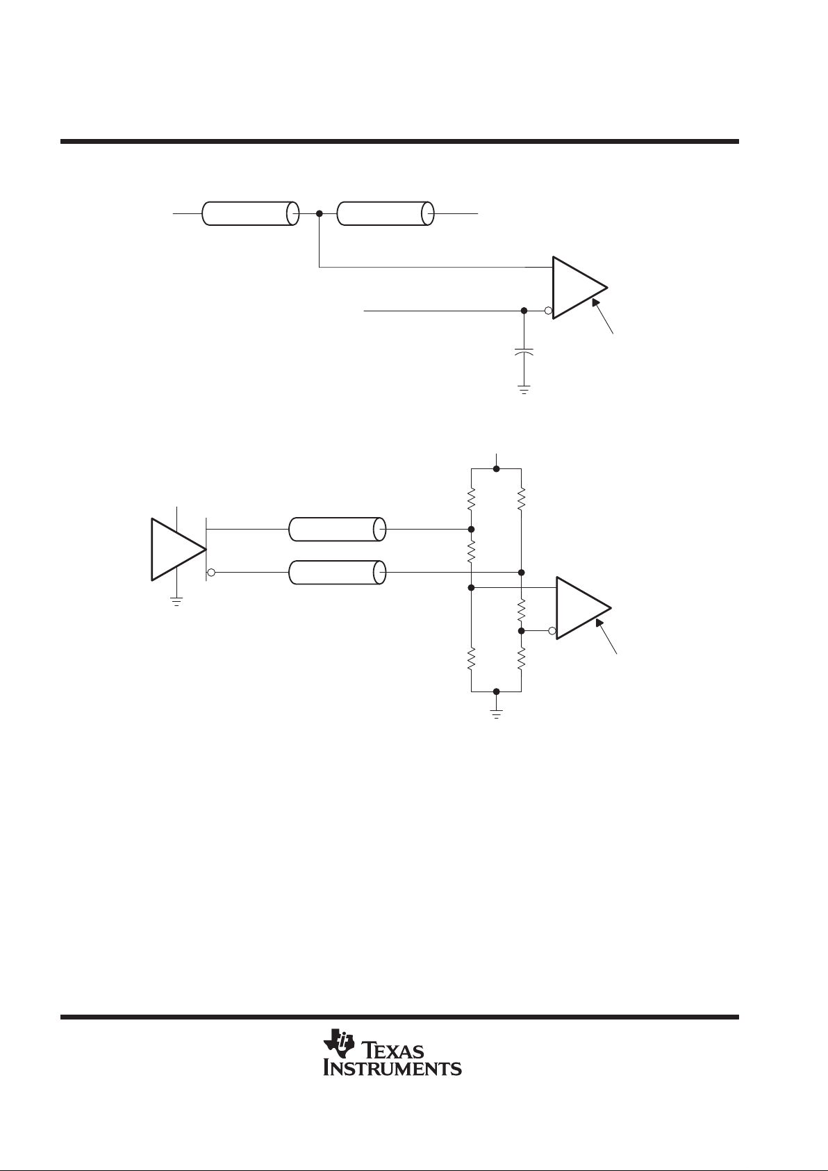
PARAMETER MEASUREMENT INFORMATION
(VOY + VOZ)/2
I
OZ
I
OY
Y
Z
V
OD
V
OY
V
OC
V
OZ
V
ID
V
IB
V
IA
I
IA
A
B
I
IB
Figure 1. Voltage and Current Definitions

SN65LVDS109, SN65LVDS117
DUAL 4-PORT AND DUAL 8-PORT LVDS REPEATERS
SLLS369C – AUGUST 1999 – REVISED MARCH 2000
8
POST OFFICE BOX 655303 • DALLAS, TEXAS 75265
PARAMETER MEASUREMENT INFORMATION
Table 1. Receiver Minimum and Maximum Input Threshold Test Voltages
APPLIED VOLTAGES RESULTING DIFFERENTIAL
INPUT VOLTAGE
RESULTING COMMONMODE INPUT VOLTAGE
V
IA
V
IB
V
ID
V
IC
1.25 V 1.15 V 100 mV 1.2 V
1.15 V 1.25 V -100 mV 1.2 V
2.4 V 2.3 V 100 mV 2.35 V
2.3 V 2.4 V -100 mV 2.35 V
0.1 V 0 V 100 mV 0.05 V
0 V 0.1 V -100 mV 0.05 V
1.5 V 0.9 V 600 mV 1.2 V
0.9 V 1.5 V -600 mV 1.2 V
2.4 V 1.8 V 600 mV 2.1 V
1.8 V 2.4 V -600 mV 2.1 V
0.6 V 0 V 600 mV 0.3 V
0 V 0.6 V -600 mV 0.3 V
±
3.75 kΩ
0 V ≤ V
TEST
≤ 2.4 V
Y
Z
V
OD
Input
100 Ω
3.75 kΩ
Figure 2. VOD Test Circuit
Y
Z
Input
50 pF
49.9 Ω ± 1% (2 Places)
V
OC
V
O
V
OC(PP)
V
OC(SS)
1 V
1.4 V
V
I
Input
V
I
NOTE A: All input pulses are supplied by a generator having the following characteristics: tr or tf ≤ 1 ns, pulse repetition rate (PRR) = 0.5 Mpps,
pulsewidth = 500 ±10 ns. CL includes instrumentation and fixture capacitance within 0,06 mm of the D.U.T . The measurement of V
OC(PP)
is made on test equipment with a –3 dB bandwidth of at least 300 MHz.
Figure 3. Test Circuit and Definitions for the Driver Common-Mode Output Voltage

SN65LVDS109, SN65LVDS117
DUAL 4-PORT AND DUAL 8-PORT LVDS REPEATERS
SLLS369C – AUGUST 1999 – REVISED MARCH 2000
9
POST OFFICE BOX 655303 • DALLAS, TEXAS 75265
PARAMETER MEASUREMENT INFORMATION
Y
Z
V
OD
Input
CL = 10 pF
(2 Places)
100 Ω ± 1 %
1.4 V
1.2 V
1 V
t
PLH
t
PHL
100%
80%
20%
0%
Input
Output
0 V
t
f
t
r
V
OD(H)
V
OD(L)
V
IB
V
IA
A
B
NOTE A: All input pulses are supplied by a generator having the following characteristics: tr or tf ≤ 1 ns, pulse repetition rate (PRR) = 50 Mpps,
pulsewidth = 10 ±0.2 ns . CL includes instrumentation and fixture capacitance within 0,06 mm of the D.U.T.
Figure 4. Test Circuit, Timing, and Voltage Definitions for the Differential Output Signal
CL = 10 pF
(2 Places)
Y
Z
Inputs
49.9 Ω ± 1% (2 Places)
t
PZH
t
PHZ
t
PZL
t
PLZ
2 V
1.4 V
0.8 V
100%, ≅ 1.4 V
50%
0%, 1.2 V
0%, ≅ 1 V
100%, 1.2 V
50%
Input
V
OY
or
V
OZ
V
OZ
or
V
OY
V
OYVOZ
1 V or 1.4 V
1.4 V or 1 V
EN
1.2 V
+
–
NOTE A: All input pulses are supplied by a generator having the following characteristics: tr or tf ≤ 1 ns, pulse repetition rate (PRR) = 0.5 Mpps,
pulsewidth = 500 ±10 ns . CL includes instrumentation and fixture capacitance within 0,06 mm of the D.U.T.
Figure 5. Enable and Disable Time Circuit and Definitions

SN65LVDS109, SN65LVDS117
DUAL 4-PORT AND DUAL 8-PORT LVDS REPEATERS
SLLS369C – AUGUST 1999 – REVISED MARCH 2000
10
POST OFFICE BOX 655303 • DALLAS, TEXAS 75265
TYPICAL CHARACTERISTICS
Figure 6
0
20
40
60
80
100
120
140
0 50 100 150 200 250 300 350
f – Frequency – MHz
– Supply Current – mA
I
CC
SN65LVDS109
SUPPLY CURRENT
vs
SWITCHING FREQUENCY
VCC = 3.6 V
VCC = 3 V
All Outputs Loaded
and Enabled
VCC = 3.3 V
Figure 7
80
100
120
140
160
180
200
220
0 50 100 150 200 250 300 350 400
f – Frequency – MHz
– Supply Current – mA
I
CC
SN65LVDS117
SUPPLY CURRENT
vs
SWITCHING FREQUENCY
VCC = 3.6 V
VCC = 3 V
All Outputs Loaded
and Enabled
VCC = 3.3 V
Figure 8
TA – Free–Air Temperature – °C
LOW-TO-HIGH PROPAGATION DELAY TIME
vs
FREE-AIR TEMPERATURE
3.1
3.2
3.3
3.4
3.5
3.6
3.7
3.8
–50 –25 0 25 50 75 100
t
PLH – Low-To-High Propagation Delay Time – ns
VCC = 3.6 V
VCC = 3 V
VCC = 3.3 V
Figure 9
TA – Free–Air Temperature – °C
HIGH-TO-LOW PROPAGATION DELAY TIME
vs
FREE-AIR TEMPERATURE
2.9
3.0
3.1
3.2
3.3
3.4
3.5
3.6
3.7
–50 –25 0 25 50 75 100
t
PHL – High-To-Low Propagation Delay Time – ns
VCC = 3.6 V
VCC = 3 V
VCC = 3.3 V

SN65LVDS109, SN65LVDS117
DUAL 4-PORT AND DUAL 8-PORT LVDS REPEATERS
SLLS369C – AUGUST 1999 – REVISED MARCH 2000
11
POST OFFICE BOX 655303 • DALLAS, TEXAS 75265
TYPICAL CHARACTERISTICS
Figure 10. Typical Differential Eye Pattern at 400 Mbps

SN65LVDS109, SN65LVDS117
DUAL 4-PORT AND DUAL 8-PORT LVDS REPEATERS
SLLS369C – AUGUST 1999 – REVISED MARCH 2000
12
POST OFFICE BOX 655303 • DALLAS, TEXAS 75265
APPLICATION INFORMATION
The SN65LVDS109 and SN65LVDS117 devices solve several problems common to the distribution of timing
critical clock and data signals. These problems include:
D
Excessive skew between the signals
D
Noise pickup over long signaling paths
D
High power consumption
D
Control of which signal paths are enabled or disabled
D
Elimination of radiation from unterminated lines
Buffering and splitting the two related signals on the same silicon die minimizes corruption of the timing relation
between the two signals. Buffering and splitting the two signals in separate devices will introduce considerably
higher levels of uncontrolled timing skew between the two signals. Higher speed operation and more timing
tolerance for other components of the system is enabled by the tighter system timing budgets provided by the
single die implementations of the SN65LVDS109 and SN65LVDS117.
The use of L VDS signaling technology for both the inputs and the outputs provides superior common–mode and
noise tolerance compared to single-ended I/O technologies. This is particularly important because the signals
that are being distributed must be transmitted over longer distances, and at higher rates, than can be
accommodated with single-ended I/Os. In addition, LVDS consumes considerably less power than other
high-performance differential signaling schemes.
The enable inputs provided for each output pair may be used to turn on or off any of the paths. This function
is required to prevent radiation of signals from the unterminated signal lines on open connectors, such as when
boards or devices are being swapped in the end equipment. The individual bank enables are also required if
redundant paths are being utilized for reliability reasons.
The diagram below shows how a pair of clock (C) and data (D) input signals is being identically repeated out
two of the available output pairs. A third output pair is shown in the disabled state.
C
D
C
D
C
D
Output Pair Disabled
DUAL n–PORT REPEATER
C
D
DESTINATION
EQUIPMENT/
BOARD #1
DESTINATION
EQUIPMENT/
BOARD #2
DESTINATION
EQUIPMENT/
BOARD #n
SOURCE
EQUIPMENT/
BOARD
Figure 11. LVDS Repeating Splitter Application Example Showing Individual Path Control

SN65LVDS109, SN65LVDS117
DUAL 4-PORT AND DUAL 8-PORT LVDS REPEATERS
SLLS369C – AUGUST 1999 – REVISED MARCH 2000
13
POST OFFICE BOX 655303 • DALLAS, TEXAS 75265
APPLICATION INFORMATION
A L VDS receiver can be used to receive various other types of logic signals. Figure 12 through Figure 20 show the
termination circuits for SSTL, HSTL, GTL, BTL, LVPECL, PECL, CMOS, and TTL.
V
DD
50 Ω
25 Ω
50
Ω
A
B
1/2 V
DD
0.1 µF
LVDS Receiver
Figure 12. Stub-Series Terminated (SSTL) or High-Speed Transceiver Logic (HSTL)
V
DD
50 Ω
50 Ω
A
B
1.35 V < VTT < 1.65 V
0.1 µF
LVDS Receiver
Figure 13. Center-Tap Termination (CTT)
V
DD
A
B
1.14 V < VTT < 1.26 V
LVDS Receiver
2 kΩ
50 Ω
0.1 µF
50 Ω1 kΩ
Figure 14. Gunning Transceiver Logic (GTL)
SN65LVDS109, SN65LVDS117
DUAL 4-PORT AND DUAL 8-PORT LVDS REPEATERS
SLLS369C – AUGUST 1999 – REVISED MARCH 2000
14
POST OFFICE BOX 655303 • DALLAS, TEXAS 75265
APPLICATION INFORMATION
A
B
1.47 V < VTT < 1.62 V
0.1 µF
LVDS Receiver
Z
0
Z
0
Figure 15. Backplane Transceiver Logic (BTL)
3.3 V
33 Ω
A
B
3.3 V
LVDS Receiver
33 Ω
51 Ω
ECL
50 Ω
50 Ω
51 Ω
120 Ω120 Ω
Figure 16. Low-Voltage Positive Emitter-Coupled Logic (LVPECL)

SN65LVDS109, SN65LVDS117
DUAL 4-PORT AND DUAL 8-PORT LVDS REPEATERS
SLLS369C – AUGUST 1999 – REVISED MARCH 2000
15
POST OFFICE BOX 655303 • DALLAS, TEXAS 75265
APPLICATION INFORMATION
5 V
100 Ω
A
B
5 V
LVDS Receiver
100 Ω
33 Ω
ECL
50 Ω
50 Ω
33 Ω
82 Ω82 Ω
Figure 17. Positive Emitter-Coupled Logic (PECL)
3.3 V
A
B
3.3 V
LVDS Receiver
7.5 kΩ
0.1 µF
7.5 kΩ
Figure 18. 3.3-V CMOS

SN65LVDS109, SN65LVDS117
DUAL 4-PORT AND DUAL 8-PORT LVDS REPEATERS
SLLS369C – AUGUST 1999 – REVISED MARCH 2000
16
POST OFFICE BOX 655303 • DALLAS, TEXAS 75265
APPLICATION INFORMATION
5 V
A
B
5 V
LVDS Receiver
3.32 kΩ
0.1 µF
10 kΩ
560 Ω
560 Ω
Figure 19. 5-V CMOS
5 V
A
B
5 V
LVDS Receiver
4.02 kΩ
0.1 µF
10 kΩ
470 Ω
3.3 V
Figure 20. TTL

SN65LVDS109, SN65LVDS117
DUAL 4-PORT AND DUAL 8-PORT LVDS REPEATERS
SLLS369C – AUGUST 1999 – REVISED MARCH 2000
17
POST OFFICE BOX 655303 • DALLAS, TEXAS 75265
MECHANICAL DATA
DBT (R-PDSO-G**) PLASTIC SMALL-OUTLINE PACKAGE
30 PINS SHOWN
0,75
0,25
0,50
0,15 NOM
Gage Plane
50
12,60
38
9,80 11,10
44
12,409,60 10,90
4073252/D 09/97
4,30
4,50
0,27
0,17
16
15
30
A
1
7,90
30
DIM
A MAX
PINS **
7,70
A MIN
1,20 MAX
6,60
6,20
Seating Plane
0,10
0,50
M
0,08
0°–8°
7,90
28
7,70
0,15
0,05
NOTES: A. All linear dimensions are in millimeters.
B. This drawing is subject to change without notice.
C. Body dimensions do not include mold flash or protrusion.
D. Falls within JEDEC MO-153

SN65LVDS109, SN65LVDS117
DUAL 4-PORT AND DUAL 8-PORT LVDS REPEATERS
SLLS369C – AUGUST 1999 – REVISED MARCH 2000
18
POST OFFICE BOX 655303 • DALLAS, TEXAS 75265
MECHANICAL DATA
DGG (R-PDSO-G**) PLASTIC SMALL-OUTLINE PACKAGE
4040078/F 12/97
48 PINS SHOWN
0,25
0,15 NOM
Gage Plane
6,00
6,20
8,30
7,90
0,75
0,50
Seating Plane
25
0,27
0,17
24
A
48
1
1,20 MAX
M
0,08
0,10
0,50
0°–8°
56
14,10
13,90
48
DIM
A MAX
A MIN
PINS **
12,40
12,60
64
17,10
16,90
0,15
0,05
NOTES: A. All linear dimensions are in millimeters.
B. This drawing is subject to change without notice.
C. Body dimensions do not include mold protrusion not to exceed 0,15.
D. Falls within JEDEC MO-153

IMPORTANT NOTICE
T exas Instruments and its subsidiaries (TI) reserve the right to make changes to their products or to discontinue
any product or service without notice, and advise customers to obtain the latest version of relevant information
to verify, before placing orders, that information being relied on is current and complete. All products are sold
subject to the terms and conditions of sale supplied at the time of order acknowledgment, including those
pertaining to warranty, patent infringement, and limitation of liability.
TI warrants performance of its semiconductor products to the specifications applicable at the time of sale in
accordance with TI’s standard warranty. Testing and other quality control techniques are utilized to the extent
TI deems necessary to support this warranty. Specific testing of all parameters of each device is not necessarily
performed, except those mandated by government requirements.
Customers are responsible for their applications using TI components.
In order to minimize risks associated with the customer’s applications, adequate design and operating
safeguards must be provided by the customer to minimize inherent or procedural hazards.
TI assumes no liability for applications assistance or customer product design. TI does not warrant or represent
that any license, either express or implied, is granted under any patent right, copyright, mask work right, or other
intellectual property right of TI covering or relating to any combination, machine, or process in which such
semiconductor products or services might be or are used. TI’s publication of information regarding any third
party’s products or services does not constitute TI’s approval, warranty or endorsement thereof.
Copyright 2000, Texas Instruments Incorporated
 Loading...