

Page 1
查询PCI1131供应商
D
3.3-V Core Logic With Universal PCI
Interface Compatible With 3.3-V or 5-V PCI
Signaling Environments
D
Supports PCI Local Bus Specification 2.1
D
Mix-and-Match 3.3-V/5-V PC Card16 Cards
and 3.3-V CardBus Cards
D
Supports T wo PC Card or CardBus Slots
With Hot Insertion and Removal
D
1995 PC Card-Standard Compliant
D
Low-Power Advanced Submicron CMOS
T echnology
D
Uses Serial Interface to Texas Instruments
(TI) TPS2206 Dual Power Switch
D
System Interrupts Can Be Programmed as
PCI-Style or ISA IRQ-Style Interrupts
D
ISA IRQ Interrupts Can Be Serialized Onto a
Single IRQSER Pin
D
Programmable Output Select for CLKRUN
D
Supports Burst Transfers to Maximize Data
Throughput on the PCI and CardBus Bus
D
Multifunction PCI Device With Separate
Configuration Spaces for Each Socket
PCI-TO-CARDBUS CONTROLLER UNIT
XCPS011 – DECEMBER 1997
D
Five PCI Memory Windows and T wo I/O
Windows Available to Each PC Card16
Socket
D
Two I/O Windows and Two Memory
Windows Available to Each CardBus
Socket
D
CardBus Memory Windows Can Be
Individually Selected Prefetchable or
Nonprefetchable
D
Exchangeable Card Architecture
(ExCA)-Compatible Registers Mapped in
Memory or I/O Space
D
TI Extension Registers Mapped in the PCI
Configuration Space
D
Intel 82365SL-DF Register Compatible
D
Supports 16-Bit Distributed Direct Memory
Access (DMA) on Both PC Card Sockets
D
Supports PC/PCI DMA on Both PC Card
Sockets
D
Supports Zoom Video Mode
D
Supports Ring Indicate
D
Packaged in 208-Pin Thin Plastic Quad
Flatpack
PCI1131
Table of Contents
Description 2. . . . . . . . . . . . . . . . . . . . . . . . . . . . . . . . . . . . . . . . . . . .
System Block Diagram 3. . . . . . . . . . . . . . . . . . . . . . . . . . . . . . . . . .
Terminal Assignments – PCI-to-PC Card (16 Bit) 4. . . . . . . . . . . .
Terminal Assignments – PCI-to-CardBus Card 5. . . . . . . . . . . . . .
Terminal Functions 6. . . . . . . . . . . . . . . . . . . . . . . . . . . . . . . . . . . . .
Absolute Maximum Ratings 15. . . . . . . . . . . . . . . . . . . . . . . . . . . . .
Recommended Operating Conditions 15. . . . . . . . . . . . . . . . . . . .
Recommended Operating Conditions for PCI Interface 15. . . . .
Recommended Operating Conditions for PC Cards A and B 16.
Electrical Characteristics 17. . . . . . . . . . . . . . . . . . . . . . . . . . . . . . .
Please be aware that an important notice concerning availability, standard warranty, and use in critical applications of
Texas Instruments semiconductor products and disclaimers thereto appears at the end of this data sheet.
Intel and MPIIX are trademarks of Intel Corporation.
PC Card is a trademark of Personal Computer Memory Card International Association (PCMCIA).
TI is a trademark of Texas Instruments Incorporated.
PRODUCTION DATA information is current as of publication date.
Products conform to specifications per the terms of Texas Instruments
standard warranty. Production processing does not necessarily include
testing of all parameters.
PCI Clock/Reset Timing Requirements 18. . . . . . . . . . . . . . . . . . . . . .
PCI Timing Requirements 18. . . . . . . . . . . . . . . . . . . . . . . . . . . . . . . . .
Parameter Measurement Information 19. . . . . . . . . . . . . . . . . . . . . . . .
PCI Bus Parameter Measurement Information 20. . . . . . . . . . . . . . . .
PCI Card Cycle Timing 21. . . . . . . . . . . . . . . . . . . . . . . . . . . . . . . . . . . .
Timing Requirements 22. . . . . . . . . . . . . . . . . . . . . . . . . . . . . . . . . . . . .
Switching Characteristics 23. . . . . . . . . . . . . . . . . . . . . . . . . . . . . . . . . .
PC Card Parameter Measurement Information 23. . . . . . . . . . . . . . . .
Mechanical Data 25. . . . . . . . . . . . . . . . . . . . . . . . . . . . . . . . . . . . . . . . .
Copyright 1997, Texas Instruments Incorporated
POST OFFICE BOX 655303 • DALLAS, TEXAS 75265
1
Page 2

PCI1131
PCI-TO-CARDBUS CONTROLLER UNIT
XCPS011 – DECEMBER 1997
description
The TI PCI1131 is a high-performance PCI-to-PC Card controller that supports two independent PC Card
sockets compliant with the 1995 PC Card standard. The PCI1 131 provides a set of features that makes it ideal
for bridging between PCI and PC Cards in both notebook and desktop computers. The 1995 PC Card standard
retains the 16-bit PC Card specification defined in PCMCIA release 2.1 and defines the new 32-bit PC Card,
called CardBus, capable of full 32-bit data transfers at 33 MHz. The PCI1 131 supports any combination of 16-bit
and CardBus PC Cards in its two sockets, powered at 3.3 V or 5 V, as required.
The PCI1 131 is compliant with the PCI local bus specification revision 2.1, and its PCI interface can act as either
a PCI master device or a PCI slave device. The PCI bus mastering is initiated during 16-bit PC Card DMA
transfers or CardBus PC Card bus-mastering cycles.
All card signals are internally buffered to allow hot insertion and removal without external buffering. The PCI1 131
is register compatible with the Intel 82365SL-DF ExCA controller. The PCI1131 internal datapath logic allows
the host to access 8-, 16-, and 32-bit cards using full 32-bit PCI cycles for maximum performance. Independent
32-bit write buffers allow fast-posted writes to improve system-bus utilization.
An advanced CMOS process is used to achieve low system-power consumption while operating at PCI clock
rates up to 33 MHz. Several low-power modes allow the host power-management system to further reduce
power consumption.
All unused PCI1131 inputs should be pulled high through a 43-kΩ resistor.
2
POST OFFICE BOX 655303 • DALLAS, TEXAS 75265
Page 3
PCI-TO-CARDBUS CONTROLLER UNIT
XCPS011 – DECEMBER 1997
system block diagram
A simplified system block diagram using the PCI1131 is provided below. The PCI950 IRQ deseralizer and the
PCI930 zoomed video (ZV) switch are optional functions that can be used when the system requires that
capability.
The PCI interface includes all address/data and control signals for PCI protocol. The 68-pin PC Card interface
includes all address/data and control signals for CardBus and 16-bit (R2) protocols. When zoomed video (ZV)
is enabled (in 16-bit PC Card mode) 23 of the 68 signals are redefined to support the ZV protocol.
The interrupt interface includes terminals for parallel PCI, parallel ISA, and serialized PCI and ISA signaling.
Other miscellaneous system interface terminals are available on the PCI1131 that include:
D
Multifunction IRQ terminals
D
SUSPEND, RI_OUT (power management control signals)
D
SPKROUT.
PCI Bus
PCI1131
INTA
INTB
TPS22xx
Power
Switch
PC Card
Socket A
PC Card
Socket B
External ZV Port
NOTE: The PC Card interface is 68 pins for CardBus and 16-bit PC Cards. In zoomed-video mode 23 pins are used for routing the zoomed
video signals too the VGA controller.
3
PCI1131
68 68
23
23
IRQSER
3
PCI930
ZV Switch
PCI950
IRQSER
Deserializer
Zoom Video
19
Zoom Video
4
Interrupt
Controller
IRQ2–15
VGA
Controller
Audio
Sub-System
POST OFFICE BOX 655303 • DALLAS, TEXAS 75265
3
Page 4
PCI1131
PCI-TO-CARDBUS CONTROLLER UNIT
XCPS011 – DECEMBER 1997
terminal assignments – PCI-to-PC Card (16 bit)
PDV PACKAGE
(TOP VIEW)
IRQ7/PCDMAREQ
IRQ9/IRQSER
IRQ10/CLKRUN
IRQ11/PCDMAGNT
IRQ12/CLKRUN
IRQ14
IRQ15/RI_OUT
V
PCLK
RSTIN
GND
GNT
REQ
AD31
AD30
V
CCP
AD29
AD28
V
AD27
AD26
AD25
AD24
C/BE3
GND
IDSEL
AD23
AD22
AD21
AD20
V
AD19
AD18
AD17
AD16
C/BE2
FRAME
GND
IRDY
TRDY
DEVSEL
STOP
PERR
SERR
V
PAR
C/BE1
AD15
AD14
AD13
GND
AD12
A_D10
A_D2
146
147
AD3
AD4
A_D9
144
145
AD2
CC
A_D1
V
143
GND
A_D8
142
AD1
A_CD2
A_D0
A_BVD1(STSCHG/RI)
A_WP(IOIS16)
138
140
139
141
AD0
B_D3
B_D11
B_CD1
A_BVD2(SPKR)
A_WAIT
A_VS1
A_READY(IREQ)
134
136
135
137
GND
B_D4
B_D5
B_D13
B_D12
A_A0
PCI1131 CorePCI
B_D6
133
A_A2
A_A1
132
131
B_D7
B_D14
A_REG
GND
130
129
B_D15
B_CE1
A_INPACK
A_A3
128
127
B_A10
B_CE2
A_A4
A_A5
126
125
Card A
Card B
CC
V
B_OE
IRQ3/INTA
154
AD9
GND
153
AD8
152
151
C/BE0
AD7
LATCH
V
SPKROUT/SUPEND
148
150
149
CC
AD6
AD5
V
IRQ4/INTB
IRQ5
156
155
157
158
159
160
161
162
163
164
CC
165
166
167
168
169
170
171
172
173
174
175
CC
176
177
178
179
180
181
182
183
184
185
186
CC
187
188
189
190
191
192
193
194
195
196
197
198
199
200
201
CC
202
203
204
205
206
207
208
214365871091211141316151817201922212423262528273029323134333635383740394241444346454847504952
AD11
AD10
CCP
DATA
CLOCK
A_A6
A_RESET
A_VS2
122
124
123
B_A11
B_IORD
B_IOWR
CCA
A_A25
V
120
121
B_A9
B_A17
A_A7
119
CCB
V
A_A12
A_A24
118
117
B_A8
B_A18
A_A15
A_A23
116
115
B_A19
B_A13
A_A22
V
114
113
GND
B_A14
CC
112
A_A16
A_A21
111
B_WE
B_A20
A_WE
A_A20
110
109
B_A21
A_A14
108
B_A16
B_A22
A_A13
A_A19
106
107
51
B_A15
B_A23
A_A18
105
A_A8
104
A_A17
103
102
A_A9
101
A_IOWR
100
A_A11
99
A_IORD
98
A_OE
97
A_CE2
96
GND
95
A_A10
94
A_CE1
93
A_D15
92
A_D7
A_D14
91
A_D6
90
A_D13
89
A_D5
88
A_D12
87
86
V
CC
A_D4
85
A_D11
84
A_D3
83
A_CD1
82
81
B_D10
80
B_D2
B_D9
79
B_D1
78
B_D8
77
76
B_D0
GND
75
B_CD2
74
B_WP(IOIS16)
73
B_BVD1(STSCHG/RI)
72
B_BVD2(SPKR)
71
B_WAIT
70
B_READY(IREQ)
69
B_VS1
68
B_A0
67
B_A1
66
B_A2
65
V
CC
64
B_REG
63
62
B_A3
B_INPACK
61
B_A4
60
B_A5
59
B_RESET
58
B_A6
57
B_VS2
56
55
B_A25
54
B_A7
B_A24
53
B_A12
4
POST OFFICE BOX 655303 • DALLAS, TEXAS 75265
Page 5
terminal assignments – PCI-to-CardBus Card
PDV PACKAGE
PCI1131
PCI-TO-CARDBUS CONTROLLER UNIT
XCPS011 – DECEMBER 1997
(TOP VIEW)
IRQ7/PCDMAREQ
IRQ9/IRQSER
IRQ10/CLKRUN
IRQ11/PCDMAGNT
IRQ12/CLKRUN
IRQ14
IRQ15/RI_OUT
V
PCLK
RSTIN
GND
GNT
REQ
AD31
AD30
V
CCP
AD29
AD28
V
AD27
AD26
AD25
AD24
C/BE3
GND
IDSEL
AD23
AD22
AD21
AD20
V
AD19
AD18
AD17
AD16
C/BE2
FRAME
GND
IRDY
TRDY
DEVSEL
STOP
PERR
SERR
V
PAR
C/BE1
AD15
AD14
AD13
GND
AD12
A_CAD31
A_CAD30
A_RSVD
146
145
147
AD4
AD3
AD2
CC
A_CAD28
A_CAD29
V
142
144
143
AD1
AD0
GND
A_CCD2
A_CAD27
A_CCLKRUN
140
139
141
B_CAD2
B_CAD0
B_CCD1
A_CAUDIO
A_CSTSCHG
A_CSERR
A_CINT
136
135
138
137
GND
B_CAD6
B_CAD3
B_CAD1
B_CAD4
A_CVS1
A_CAD26
134
133
PCI1131 CorePCI
B_CAD5
B_RSVD
A_CAD24
A_CC/BE3
A_CAD25
130
129
132
131
B_CAD8
B_CAD7
B_CC/BE0
A_CREQ
A_CAD23
GND
128
127
B_CAD9
B_CAD10
A_CAD22
A_CRST
A_CAD21
124
126
125
Card A
Card B
CC
V
B_CAD11
B_CAD13
A_CAD19
A_CAD20
A_CVS2
122
121
123
B_CAD14
B_CAD15
B_CAD12
CCA
A_CAD18
A_CAD17
V
118
119
120
CCB
V
B_CAD16
B_CC/BE1
A_CC/BE2
A_CIRDY
A_CFRAME
114
116
115
117
B_CPAR
B_RSVD
B_CBLOCK
CC
A_CCLK
A_CTRDY
A_CDEVSEL
V
111
112
113
GND
B_CGNT
B_CSTOP
B_CPERR
A_CGNT
A_CSTOP
A_CPERR
A_CBLOCK
110
108
107
109
B_CCLK
B_CIRDY
B_CTRDY
B_CDEVSEL
A_CPAR
A_RSVD
106
105
104
103
102
101
100
99
98
97
96
95
94
93
92
91
90
89
88
87
86
85
84
83
82
81
80
79
78
77
76
75
74
73
72
71
70
69
68
67
66
65
64
63
62
61
60
59
58
57
56
55
54
53
51
B_CC/BE2
B_CFRAME
A_CC/BE1
A_CAD16
A_CAD14
A_CAD15
A_CAD12
A_CAD13
A_CAD11
A_CAD10
GND
A_CAD9
A_CC/BE0
A_CAD8
A_CAD7
A_RSVD
A_CAD5
A_CAD6
A_CAD3
A_CAD4
V
CC
A_CAD1
A_CAD2
A_CAD0
A_CCD1
B_CAD31
B_RSVD
B_CAD30
B_CAD29
B_CAD28
B_CAD27
GND
B_CCD2
B_CCLKRUN
B_CSTSCHG
B_CAUDIO
B_CSERR
B_CINT
B_CVS1
B_CAD26
B_CAD25
B_CAD24
V
CC
B_CC/BE3
B_CAD23
B_CREQ
B_CAD22
B_CAD21
B_CRST
B_CAD20
B_CVS2
B_CAD19
B_CAD18
B_CAD17
IRQ3/INTA
154
AD9
GND
153
AD8
152
151
C/BE0
AD7
LATCH
150
CC
V
V
SPKROUT/SUSPEND
148
149
AD6
AD5
IRQ4/INTB
IRQ5
156
155
157
158
159
160
161
162
163
164
CC
165
166
167
168
169
170
171
172
173
174
175
CC
176
177
178
179
180
181
182
183
184
185
186
CC
187
188
189
190
191
192
193
194
195
196
197
198
199
200
201
CC
202
203
204
205
206
207
208
214365871091211141316151817201922212423262528273029323134333635383740394241444346454847504952
AD11
AD10
CCP
DATA
CLOCK
POST OFFICE BOX 655303 • DALLAS, TEXAS 75265
5
Page 6
PCI1131
FUNCTION
FUNCTION
PCI-TO-CARDBUS CONTROLLER UNIT
XCPS011 – DECEMBER 1997
Terminal Functions
PCI system
TERMINAL
NAME NO.
PCLK 165 I
RSTIN
166 I
PCI address and data
TERMINAL
NAME NO.
AD31
AD30
AD29
AD28
AD27
AD26
AD25
AD24
AD23
AD22
AD21
AD20
AD19
AD18
AD17
AD16
AD15
AD14
AD13
AD12
AD11
AD10
AD9
AD8
AD7
AD6
AD5
AD4
AD3
AD2
AD1
AD0
C/BE3
C/BE2
C/BE1
C/BE0
PAR 202 I/O
170
171
173
174
176
177
178
179
183
184
185
186
188
189
190
191
204
205
206
208
180
192
203
10
11
12
14
15
I/O
TYPE
PCI bus clock. PCLK provides timing for all transactions on the PCI bus. All PCI signals are sampled at the rising
edge of PCLK.
PCI reset. When the RSTIN signal is asserted low, the PCI1131 forces all output buffers to the high-impedance
state and resets all internal registers. When asserted, the PCI1131 is nonfunctional. After RSTIN
the PCI1131 returns to the default state. When the PCI1131 SUSPEND
from any RSTIN
I/O
TYPE
Address/data bus. AD31–AD0 are the multiplexed PCI address and data bus. During the address phase of a PCI
cycle, AD31–AD0 contain a 32-bit address or other destination information. During the data phase, AD31–AD0
I/O
contain data.
1
2
3
4
6
8
9
Bus commands and byte enables. C/BE3–C/BE0 are multiplexed on the same PCI terminals. During the address
phase, C/BE3
I/O
5
The byte enables determine which byte lanes carry meaningful data. C/BE0
applies to byte 1 (AD15–AD8), C/BE2 applies to byte 2 (AD23–AD16), and C/BE3 applies to byte 3 (AD31–AD24).
Parity. As a PCI target during PCI read cycles, or as PCI bus master during PCI write cycles, the PCI1 131 calculates
even parity across the AD and C/BE
reset (i.e., the PCI1131 internal register contents are preserved).
–C/BE0 define the bus command. During the data phase, C/BE3–C/BE0 are used as byte enables.
is deasserted,
mode is enabled, the device is protected
applies to byte 0 (AD7–AD0), C/BE1
buses and outputs the results on PAR, delayed by one clock.
6
POST OFFICE BOX 655303 • DALLAS, TEXAS 75265
Page 7
FUNCTION
FUNCTION
PCI interface control
TERMINAL
NAME NO.
DEVSEL
FRAME
GNT
IDSEL 182 I
IRDY
IRQ10/CLKRUN
IRQ12/CLKRUN
PERR
REQ
SERR
STOP
TRDY
197 I/O
193 I/O
168 I
195 I/O
159
161
199 I/O
169 O Request. REQ is asserted by the PCI1131 to request access to the PCI bus as a master.
200 O System error. SERR pulsed from the PCI1131 indicates an address parity error has occurred.
198 I/O Stop. STOP is driven by the current PCI target to request the master to stop the current transaction.
196 I/O
I/O
TYPE
I/O
PCI1131
PCI-TO-CARDBUS CONTROLLER UNIT
XCPS011 – DECEMBER 1997
Terminal Functions (Continued)
Device select. As a PCI target, the PCI1131 asserts DEVSEL to claim the current cycle. As a PCI master,
the PCI1131 monitors DEVSEL
Cycle frame. FRAME is driven by the current master to indicate the beginning and duration of an access,
FRAME
is low (asserted) to indicate that a bus transaction is beginning. While FRAME is asserted, data
transfers continue. When FRAME
Grant. GNT is driven by the PCI arbiter to grant the PCI1131 access to the PCI bus after the current data
transaction is complete.
Initialization device select. IDSEL selects the PCI1131 during configuration accesses. IDSEL can be
connected to one of the upper 24 PCI address lines.
Initiator ready. IRDY indicates the bus master ’s ability to complete the current data phase of the
transaction. IRDY
are sampled low (asserted). During a write, IRDY indicates that valid data is present on
TRDY
AD31–AD0. During a read, IRDY
inserted until both IRDY
the PCI1131 is the PCI bus master and an input when the PCI bus is the target.
Interrupt request 10 and 12. IRQ10/CLKRUN and IRQ12/CLKRUN are software configurable and used
by the PCI1131 to support the PCI clock run protocol. When configured as CLKRUN
the system control register offset 80h, this terminal is an open-drain output. To select between IRQ10
and IRQ12 as the output, use bit 7 of register 80h.
Parity error. PERR is driven by the PCI target during a write to indicate that a data parity error has been
detected.
Target ready. TRDY indicates the ability of the PCI1131 to complete the current data phase of the
transaction. TRDY
are sampled asserted. During a read, TRDY indicates that valid data is present on AD31–AD0.
IRDY
During a write, TRDY
both IRDY
and an input when the PCI1131 is the PCI bus master.
is used with TRDY. A data phase is completed on any clock where both IRDY and
is used with IRDY. A data phase is completed on any clock where both TRDY and
indicates that the PCI1131 is prepared to accept data. W ait cycles are inserted until
and TRDY are asserted together. This signal is an output when the PCI1 131 is the PCI target
until a target responds or a time-out occurs.
is sampled high (deasserted), the transaction is in the final data phase.
indicates that the master is prepared to accept data. Wait cycles are
and TRDY are low (asserted) at the same time. This signal is an output when
by setting bit 0 in
power supply
TERMINAL
NAME NO.
GND 13, 22, 44, 75, 96, 129, 153, 167, 181, 194, 207 Device ground terminals
V
V
V
V
CC
CCA
CCB
CCP
7, 31, 64, 86, 113, 143, 164, 175, 187, 201 Power supply terminal for core logic (3.3 V)
120 Power supply terminal for PC Card A (5 V or 3.3 V)
38 Power supply terminal for PC Card B (5 V or 3.3 V)
148, 172 Power supply terminal for PCI interface (5 V or 3.3 V)
POST OFFICE BOX 655303 • DALLAS, TEXAS 75265
7
Page 8
PCI1131
FUNCTION
FUNCTION
FUNCTION
PCI-TO-CARDBUS CONTROLLER UNIT
XCPS011 – DECEMBER 1997
Terminal Functions (Continued)
PC Card power switch
TERMINAL
NAME NO.
CLOCK 151 O
DATA 152 O Power switch data. DATA is used by the PCI1 131 to serially communicate socket power control information.
LATCH 150 O
interrupt
TERMINAL
NAME NO.
IRQ3/INTA
IRQ4/INTB
IRQ7/PCDMAREQ 157 O
IRQ9/IRQSER
IRQ10/CLKRUN
IRQ12/CLKRUN
IRQ11/PCDMAGNT 160 I/O
IRQ5
IRQ14
IRQ15/RI_OUT 163 I/O
I/O
TYPE
154
155
158
159
161
156
162
Power switch clock. Information on the DATA line is sampled at the rising edge of CLOCK. The frequency of
the clock is derived from dividing PCICLK by 36. The maximum frequency of CLOCK is 2 MHz.
Power switch latch. LATCH is asserted by the PCI1131 to indicate to the PC Card power switch that the data
on the DATA line is valid.
I/O
TYPE
Interrupt request 3 and interrupt request 4. IRQ3/INTA–IRQ4/INTB can be connected to either PCI
or ISA interrupts. IRQ3/INTA
. When configured for IRQ3 and IRQ4, IRQ3/INTA–IRQ4/INTB must be connected to the ISA
or INTB
O
IRQ programmable interrupt controller. When IRQ3/INTA
INTB
, IRQ3/INTA–IRQ4/INTB must be connected to interrupts on the PCI bus.
Interrupt request 7. IRQ7/PCDMAREQ is software configurable and is used by the PCI1131 to
request PC/PCI DMA transfers from chipsets that support the PC/PCI DMA scheme. When
IRQ7/PCDMAREQ
appropriate request (REQ
Interrupt request 9/serial IRQ. IRQ9/IRQSER is software configurable and indicates an interrupt
request from a PC Card to the PCI1131. When IRQ9/IRQSER is configured for IRQ9, it must be
connected to the system programmable interrupt controller. IRQSER allows all IRQ signals to be
O
serialized onto one pin. IRQ9/IRQSER is configured via bits 2–1 in the device control register of the
I/O
TI extension registers.
Interrupt request 10 and 12. IRQ10/CLKRUN and IRQ12/CLKRUN are software configurable and
used by the PCI1131 to support the PCI clock run protocol. When configured as CLKRUN
I/O
bit 0 in the system control register offset 80h, this terminal is an open-drain output. T o select between
IRQ10 and IRQ12 as the output, use bit 7 of register 80h.
Interrupt request 11. IRQ11/PCDMAGNT is software configurable and is used by the PCI1131 to
accept a grant for PC/PCI DMA transfers from chipsets that support the PC/PCI DMA scheme. When
IRQ11/PCDMAGNT
appropriate grant (GNT
Interrupt request 5 and 14. These signals are ISA interrupts. These terminals indicate an interrupt
request from one of the PC Cards. The interrupt mode is selected in the device control register of
O
the TI extension registers.
Interrupt request 15. IRQ15/RI_OUT indicates an interrupt request from one of the PC Cards.
RI_OUT
allows the RI input from the 16-bit PC Card to be output to the system. IRQ15/RI_OUT is
configured in the card control register of the TI extension registers.
is configured for PC/PCI DMA request (IRQ7), it must be connected to the
–IRQ4/INTB are software configurable as IRQ3 or INTA and as IRQ4
–IRQ4/INTB are configured for INTA and
) pin on the Intel Mobile Triton PCI I/O accelerator (MPIIX).
is configured for PC/PCI DMA grant (IRQ11), it must be connected to the
) pin on the Intel MPIIX controller.
by setting
speaker control
TERMINAL
NAME NO.
SPKROUT/
SUSPEND
8
149 O
I/O
TYPE
Speaker. SPKROUT carries the digital audio signal from the PC Card. SUSPEND places the PCI1131 in
suspend mode. SPKROUT/SUSPEND
POST OFFICE BOX 655303 • DALLAS, TEXAS 75265
is configured in the card control register of the TI extension registers.
Page 9

FUNCTION
PCI-TO-CARDBUS CONTROLLER UNIT
Terminal Functions (Continued)
16-bit PC Card address and data (slots A and B)
TERMINAL
NUMBER
NAME
A25
A24
A23
A22
A21
A20
A19
A18
A17
A16
A15
A14
A13
A12
A10
D15
D14
D13
D12
D10
†
Terminal name is preceded with A_. For example, the full name for terminal 121 is A_A25.
‡
Terminal name is preceded with B_. For example, the full name for terminal 55 is B_A25.
A11
A9
A8
A7
A6
A5
A4
A3
A2
A1
A0
D11
D9
D8
D7
D6
D5
D4
D3
D2
D1
D0
SLOT
†
A
121
118
116
114
111
109
107
105
103
112
115
108
106
117
100
95
102
104
119
123
125
126
128
131
132
133
93
91
89
87
84
147
145
142
92
90
88
85
83
146
144
141
SLOT
I/O
TYPE
‡
B
55
53
51
49
47
45
42
40
37
48
50
43
41
52
34
29
36
39
54
57
59
60
62
65
66
67
27
25
23
20
18
81
79
77
26
24
21
19
17
80
78
76
O PC Card address. 16-bit PC Card address lines. A25 is the most-significant bit.
I/O PC Card data. 16-bit PC Card data lines. D15 is the most-significant bit.
PCI1131
XCPS011 – DECEMBER 1997
POST OFFICE BOX 655303 • DALLAS, TEXAS 75265
9
Page 10
PCI1131
FUNCTION
PCI-TO-CARDBUS CONTROLLER UNIT
XCPS011 – DECEMBER 1997
Terminal Functions (Continued)
16-bit PC Card interface control signals (slots A and B)
TERMINAL
28
30
I/O
TYPE
‡
Battery voltage detect 1. Generated by 16-bit memory PC Cards that include batteries. BVD1
is used with BVD2 as an indication of the condition of the batteries on a memory PC Card. Both
BVD1 and BVD2 are kept high when the battery is good. When BVD2 is low and BVD1 is high,
the battery is weak and needs to be replaced. When BVD1 is low, the battery is no longer
serviceable and the data in the memory PC Card is lost.
Status change. STSCHG
or battery voltage dead condition of a 16-bit I/O PC Card.
Ring indicate. RI is used by 16-bit modem cards to indicate ring detection.
Battery voltage detect 2. Generated by 16-bit memory PC Cards that include batteries. BVD2
is used with BVD1 as an indication of the condition of the batteries on a memory PC Card. Both
BVD1 and BVD2 are high when the battery is good. When BVD2 is low and BVD1 is high, the
battery is weak and needs to be replaced. When BVD1 is low, the battery is no longer
serviceable and the data in the memory PC Card is lost.
Speaker. SPKR
been configured for the 16-bit I/O interface. The audio signals from cards A and B can be
combined by the PCI1131 and output on SPKROUT.
DMA request. BVD2 can be used as the DMA request signal during DMA operations to a 16-bit
PC Card that supports DMA. If used, the PC Card asserts BVD2 to request a DMA operation.
PC Card detect 1 and PC Card detect 2. CD1 and CD2 are internally connected to ground on
I
the PC Card. When a PC Card is inserted into a socket, CD1
Card enable 1 and card enable 2. CE1 and CE2 enable even- and odd-numbered address
bytes. CE1 enables even-numbered address bytes, and CE2 enables odd-numbered address
O
bytes.
Input acknowledge. INP ACK is asserted by the PC Card when it can respond to an I/O read cycle
at the current address.
DMA request. INPACK
16-bit PC Card that supports DMA. If used, the PC Card asserts INP ACK
for a DMA operation.
I/O read. IORD is asserted by the PCI1 131 to enable 16-bit I/O PC Card data output during host
I/O read cycles.
DMA write. IORD
that supports DMA. The PCI1131 asserts IORD
memory.
I/O write. IOWR is driven low by the PCI1 131 to strobe write data into 16-bit I/O PC Cards during
host I/O write cycles.
DMA read. IOWR is used as the DMA read strobe during DMA operations to a 16-bit PC Card
that supports DMA. The PCI1131 asserts IOWR
PC Card.
Output enable. OE is driven low by the PCI1131 to enable 16-bit memory PC Card data output
during host memory read cycles.
DMA terminal count. OE
PC Card that supports DMA. The PCI1 131 asserts OE to indicate TC for a DMA write operation.
is an optional binary audio signal available only when the card and socket have
is used to alert the system to a change in the READY, write protect,
can be used as the DMA request signal during DMA operations to a
is used as the DMA write strobe during DMA operations from a 16-bit PC Card
is used as terminal count (TC) during DMA operations to a 16-bit
NUMBER
NAME
BVD1
(STSCHG
BVD2(SPKR)
CD1
CD2
CE1
CE2
INPACK 127 61 I
IORD
IOWR
OE 98 32 O
†
Terminal name is preceded with A_. For example, the full name for terminal 138 is A_BVD1.
‡
Terminal name is preceded with B_. For example, the full name for terminal 72 is B_BVD1.
/RI)
SLOT
SLOT
†
A
138 72 I
137 71 I
1401674
101 35 O
B
82
94
97
99 33 O
and CD2 are pulled low.
to indicate a request
during DMA transfers from the PC Card to host
during DMA transfers from host memory to the
10
POST OFFICE BOX 655303 • DALLAS, TEXAS 75265
Page 11

FUNCTION
PCI-TO-CARDBUS CONTROLLER UNIT
Terminal Functions (Continued)
16-bit PC Card interface control signals (slots A and B) (continued)
TERMINAL
NUMBER
NAME
READY(IREQ)
REG
RESET 124 58 O PC Card reset. RESET forces a hard reset to a 16-bit PC Card.
WAIT 136 70 I
WE 110 46 O
WP(IOIS16) 139 73 I
VS1
VS2
†
Terminal name is preceded with A_. For example, the full name for terminal 98 is A_OE.
‡
Terminal name is preceded with B_. For example, the full name for terminal 32 is B_OE
SLOT
SLOT
†
A
135 69 I
130 63 O
134
1226856
I/O
TYPE
‡
B
Ready. The ready function is provided by READY when the 16-bit PC Card and the host socket
are configured for the memory-only interface. READY is driven low by the 16-bit memory PC
Cards to indicate that the memory card circuits are busy processing a previous write command.
READY is driven high when the 16-bit memory PC Card is ready to accept a new data transfer
command.
Interrupt request. IREQ
on the 16-bit I/O PC Card requires service by the host software. IREQ
no interrupt is requested.
Attribute memory select. REG remains high for all common memory accesses. When REG is
asserted, access is limited to attribute memory (OE
or IOWR active). Attribute memory is a separately accessed section of card memory and is
generally used to record card capacity and other configuration and attribute information.
DMA acknowledge. REG is used as a DMA acknowledge (DACK) during DMA operations to
a 16-bit PC Card that supports DMA. The PCI1131 asserts REG
REG
is used with the DMA read (IOWR) or DMA write (IORD) strobes to transfer data.
Bus cycle wait. WAIT is driven by a 16-bit PC Card to delay the completion of (i.e., extend) the
memory or I/O cycle in progress.
Write enable. WE is used to strobe memory write data into 16-bit memory PC Cards. WE also
is used for memory PC Cards that employ programmable memory technologies.
DMA terminal count. WE is used as TC during DMA operations to a 16-bit PC Card that supports
DMA. The PCI1131 asserts WE to indicate TC for a DMA read operation.
Write protect. This signal applies to 16-bit memory PC Cards. WP reflects the status of the
write-protect switch on 16-bit memory PC Cards. For 16-bit I/O cards, WP is used for the 16-bit
port (IOIS16
I/O is 16 bits. WP applies to 16-bit I/O PC Cards. IOIS16 is asserted by the 16-bit PC Card when
the address on the bus corresponds to an address to which the 16-bit PC Card responds, and
the I/O port that is addressed is capable of 16-bit accesses.
DMA request. WP can be used as the DMA request signal during DMA operations to a 16-bit
PC Card that supports DMA. If used, the PC Card asserts WP to request a DMA operation.
Voltage sense 1 and voltage sense 2. VS1 and VS2, when used together, determine the
I/O
operating voltage of the 16-bit PC Card.
) function. The status of WP can be read from the ExCA interface status register.
is asserted by a 16-bit I/O PC Card to indicate to the host that a device
.
PCI1131
XCPS011 – DECEMBER 1997
is high (deasserted) when
or WE active) and to the I/O space (IORD
to indicate a DMA operation.
POST OFFICE BOX 655303 • DALLAS, TEXAS 75265
11
Page 12
PCI1131
FUNCTION
PCI-TO-CARDBUS CONTROLLER UNIT
XCPS011 – DECEMBER 1997
Terminal Functions (Continued)
CardBus PC Card address and data signals (slots A and B)
TERMINAL
NUMBER
NAME
CAD31
CAD30
CAD29
CAD28
CAD27
CAD26
CAD25
CAD24
CAD23
CAD22
CAD21
CAD20
CAD19
CAD18
CAD17
CAD16
CAD15
CAD14
CAD13
CAD12
CAD11
CAD10
CAD9
CAD8
CAD7
CAD6
CAD5
CAD4
CAD3
CAD2
CAD1
CAD0
CC/BE0
CC/BE1
CC/BE2
CC/BE3
CPAR 106 41 I/O
†
Terminal name is preceded with A_. For example, the full name for terminal 147 is A_CAD31.
‡
Terminal name is preceded with B_. For example, the full name for terminal 81 is B_CAD31.
SLOT
†
A
147
145
144
142
141
133
132
131
128
126
125
123
121
119
118
103
101
102
99
100
98
97
95
93
92
89
90
87
88
84
85
83
94
104
117
130
SLOT
I/O
TYPE
‡
B
81
79
78
77
76
67
66
65
62
60
59
57
55
54
53
37
35
36
33
34
32
30
29
27
26
23
24
20
21
18
19
17
28
39
52
63
CardBus PC Card address and data. CAD31–CAD0 are multiplexed address and data signals. A bus
transaction consists of an address phase followed by one or more data phases. The PCI1 131 supports
both read and write bursts.
The address phase is the clock cycle in which CFRAME
CAD31-CAD0 contain a physical address (32 bits). For I/O, this is a byte address; for configuration
I/O
and memory, it is a DWORD address.
During data phases, CAD7–CAD0 contain the least-significant byte and CAD31–CAD24 contain the
most-significant byte. Write data is stable and valid when CIRDY
valid when CTRDY
asserted.
CardBus PC Card command and byte enables. CC/BE0–CC/BE3 are multiplexed on the same pin.
During the address phase of the transaction, CC/BE3
data phase transaction, CC/BE3
I/O
entire data phase and determine the byte lanes that carry the data. CC/BE0
applies to byte 1, CC/BE2 applies to byte 2, and CC/BE3 applies to byte 3.
CardBus PC Card parity. Even parity across CAD31–CAD0 and CC/BE3–CC/BE0 is calculated and
driven by this signal. CPAR is stable and valid for one clock after the address phase. For data phases,
CPAR is stable and valid one clock after either CIRDY
is asserted on a read transaction. Once CPAR is valid, it remains valid for one clock after the
completion of the current data phase. NOTE: CP AR has the same timing as CAD31–CAD0 but delays
by one clock. When the PCI1131 is acting as an initiator, it drives CPAR for address and write data
phases; and when acting as a target, the PCI1131 drives CPAR for read data phases.
is asserted. Data is transferred during those clocks when CIRDY and CTRDY are
–CC/BE0 are used as byte enables. Byte enables are valid during the
is asserted. During the address phase,
is asserted. Read data is stable and
–CC/BE0 define the bus command. During the
applies to byte 0, CC/BE1
is asserted on a write transaction or CTRDY
12
POST OFFICE BOX 655303 • DALLAS, TEXAS 75265
Page 13

FUNCTION
FUNCTION
I
PCI-TO-CARDBUS CONTROLLER UNIT
Terminal Functions (Continued)
CardBus PC Card interface system signals (slots A and B)
TERMINAL
NUMBER
NAME
CCLK 112 48 O
CCLKRUN
CRST
SLOT
SLOT
†
A
139 73 I/O
124 58 O
I/O
TYPE
‡
B
CardBus PC Card clock. CCLK provides synchronous timing for all transactions on the CardBus PC
Card interface. All signals except CRST
2–CCD1, and CVS2–CVS1 are sampled on the rising edge of the clock, and all timing
CCD
parameters are defined with the rising edge of CCLK. The CardBus clock operates at 33 MHz but
can be stopped in the low state.
CardBus PC Card clock run. CCLKRUN is used by a CardBus PC Card to request an increase in the
CCLK frequency. It is used by the PCI1131 to indicate that the CCLK frequency is decreased.
CardBus PC Card reset. CRST is used to bring CardBus PC Card specific registers, sequencers, and
signals to a consistent state. When CRST
to the high-impedance state. Assertion can be asynchronous to CCLK, but deassertion must be
synchronous to CCLK.
(upon assertion) CCLKRUN, CINT, CSTSCHG, CAUDIO,
is asserted, all CardBus PC Card signals must be driven
PCI1131
XCPS011 – DECEMBER 1997
CardBus PC Card interface control signals (slots A and B)
TERMINAL
NUMBER
NAME
CAUDIO 137 71 I
CBLOCK
CCD1
CCD2
CDEVSEL
CFRAME
CGNT
CINT
†
Terminal name is preceded with A_. For example, the full name for terminal 112 is A_CCLK.
‡
Terminal name is preceded with B_. For example, the full name for terminal 48 is B_CCLK.
SLOT
SLOT
†
A
107 42 I/O
82 16
140 74
111 47 I/O
116 51 I/O
110 46 O
135 69 I
I/O
TYPE
‡
B
CardBus audio. CAUDIO is an optional digital output signal from a PC Card to the system speaker.
CardBus cards support two types of audio: single amplitude, binary waveform and/or pulsewidth
modulation (PWM) encoded signal. The PCI1 131 supports the binary audio mode and can output a
binary audio signal from the PC Card to SPKROUT.
CardBus lock. CBLOCK is an optional signal used to lock a particular address, ensuring a bus initiator
exclusive access. This signal is not supported on the PCI1131.
CardBus detect 1 and CardBus detect 2. CCD1 and CCD2 are used with CVS1 and CVS2 to
determine the type and voltage of the CardBus PC Card.
CardBus device select. When actively driven, CDEVSEL indicates that the PCI1131 has decoded its
address as the target of the current access. As an input, CDEVSEL
the bus has been selected.
CardBus cycle frame. CFRAME is driven by the PCI1131 or a CardBus card when it is acting as an
initiator to indicate the beginning and duration of a transaction. CFRAME
transaction is beginning, and while it is asserted, data transfer is continuous. When CFRAME
(deasserted), the transaction is in its final data phase.
CardBus grant. CGNT is driven by the PCI1131 to grant a CardBus PC Card access to the CardBus
bus after the current data transaction is complete.
CardBus interrupt. CINT is asserted low by a CardBus PC Card to request interrupt servicing from
the host.
indicates whether any device on
is asserted to indicate a bus
is high
POST OFFICE BOX 655303 • DALLAS, TEXAS 75265
13
Page 14

PCI1131
FUNCTION
I/O
gg ,g ,
PCI-TO-CARDBUS CONTROLLER UNIT
XCPS011 – DECEMBER 1997
Terminal Functions (Continued)
CardBus PC Card interface control signals (slots A and B) (continued)
TERMINAL
NUMBER
NAME
CIRDY
CPERR
CREQ
CSERR
CSTOP
CSTSCHG 138 72 I
CTRDY
CVS1 134 68
CVS2 122 56
†
Terminal name is preceded with A_. For example, the full name for terminal 115 is A_CIRDY.
‡
Terminal name is preceded with B_. For example, the full name for terminal 50 is B_CIRDY
SLOT
SLOT
†
A
115 50 I/O
108 43 I/O
127 61 I
136 70 I
109 45 I/O
114 49 I/O
I/O
TYPE
‡
B
CardBus initiator ready. CIRDY indicates that the PCI1131 is initiating the ability of the bus initiator
to complete a current data phase of the transaction. It is used with CTRDY
are sampled asserted, a data phase is completed on any clock. During a write, CIRDY
CTRDY
indicates that valid data is present on CAD31–CAD0. During a read, CIRDY indicates the PCI1 131,
as an initiator, is prepared to accept the data. W ait cycles are inserted until CIRDY
both low (asserted).
CardBus parity error. CPERR reports errors during all CardBus PC Card transactions except during
special cycles. CPERR
agent receiving data, two clocks following the data, when a data parity error is detected. CPERR
be driven active for a minimum duration of one clock for each data phase. CPERR
high for one clock before it is returned to the high-impedance state. An agent cannot report a CPERR
until it claims the access by asserting CDEVSEL and completes a data phase.
CardBus request. CREQ indicates to the arbiter that the CardBus PC Card requires use of the
CardBus bus.
CardBus system error. CSERR reports address parity error, data errors on the special cycle
command, or any other system error such that the CardBus card can no longer operate correctly.
is open drain and is actively driven for a single CardBus PC Card clock by the agent reporting
CSERR
the error. The assertion of CSERR
of all bused signals. Restoring CSERR
provided by the system designer. This pullup can take two to three clock periods to fully restore
CSERR
. The PCI1131 reports CSERR to the operating system any time it is sampled low (asserted).
CardBus stop. CSTOP indicates the current target is requesting the initiator to stop the current
transaction.
CardBus status change. CSTSCHG is used to alert the system to a change in the READY, WP, or
BVD condition of the I/O CardBus PC Card.
CardBus target ready. CTRDY indicates that the PCI1131, as a selected target, can complete a
current data phase of the transaction. CTRDY
sampled asserted, a data phase is completed on any clock. During a read, CTRDY
data is present on CAD31–CAD0. During a write, CIRDY
prepared to accept the data. Wait cycles are inserted until CIRDY
(asserted).
CardBus voltage sense 1 and voltage sense 2. CVS1 and CVS2, together with CCD1 and CCD2,
determine the operating voltage of the CardBus PC Card.
is sustained in the high-impedance state and must be driven active by the
is synchronous to the clock and meets the setup and hold times
to the deasserted state is accomplished by a weak pullup
is used with CIRDY. When both of these signals are
indicates the PCI1131, as a target, is
.
. When both CIRDY and
and CTRDY are
must
must be driven
indicates that valid
and CTRDY are both low
14
POST OFFICE BOX 655303 • DALLAS, TEXAS 75265
Page 15

V
PCI suppl
oltage
Commercial
V
VIInput voltage
V
V
§
Output
V
¶
CMOS compatible
IH
gg
¶
CMOS
tibl
PCI1131
PCI-TO-CARDBUS CONTROLLER UNIT
XCPS011 – DECEMBER 1997
absolute maximum ratings over operating temperature ranges (unless otherwise noted)
†
Supply voltage range: VCC –0.5 V to 4.6 V. . . . . . . . . . . . . . . . . . . . . . . . . . . . . . . . . . . . . . . . . . . . . . . . . . . . . . . .
V
–0.5 V to 6 V. . . . . . . . . . . . . . . . . . . . . . . . . . . . . . . . . . . . . . . . . . . . . . . . . . . . . . . .
CCP
Input voltage range, VI: Standard –0.5 V to VCC + 0.5 V. . . . . . . . . . . . . . . . . . . . . . . . . . . . . . . . . . . . . . . . . . . . .
Card A –0.5 to V
Card B –0.5 to V
CCA
CCB
+ 0.5 V. . . . . . . . . . . . . . . . . . . . . . . . . . . . . . . . . . . . . . . . . . . . . . .
+ 0.5 V. . . . . . . . . . . . . . . . . . . . . . . . . . . . . . . . . . . . . . . . . . . . . . .
Fail safe –0.5 V to VCC + 0.5 V. . . . . . . . . . . . . . . . . . . . . . . . . . . . . . . . . . . . . . . . . . . . .
Output voltage range, VO: Standard –0.5 V to VCC + 0.5 V. . . . . . . . . . . . . . . . . . . . . . . . . . . . . . . . . . . . . . . . . . .
Card A –0.5 to V
Card B –0.5 to V
CCA
CCB
+ 0.5 V. . . . . . . . . . . . . . . . . . . . . . . . . . . . . . . . . . . . . . . . . . . .
+ 0.5 V. . . . . . . . . . . . . . . . . . . . . . . . . . . . . . . . . . . . . . . . . . . .
Fail safe –0.5 V to VCC + 0.5 V. . . . . . . . . . . . . . . . . . . . . . . . . . . . . . . . . . . . . . . . . . .
Input clamp current, I
Output clamp current, I
Storage temperature range, T
Virtual junction temperature, T
†
Stresses beyond those listed under “absolute maximum ratings” may cause permanent damage to the device. These are stress ratings only, and
functional operation of the device at these or any other conditions beyond those indicated under “recommended operating conditions” is not
implied. Exposure to absolute-maximum-rated conditions for extended periods may affect device reliability.
NOTES: 1. Applies to external input and bidirectional buffers. VI > VCC does not apply to fail-safe terminals.
2. Applies to external output and bidirectional buffers. VO > VCC does not apply to fail-safe terminals.
(VI < 0 or VI > VCC) (see Note 1) ±20 mA. . . . . . . . . . . . . . . . . . . . . . . . . . . . . . . . . . . .
IK
(VO < 0 or VO > VCC) (see Note 2) ±20 mA. . . . . . . . . . . . . . . . . . . . . . . . . . . . . . . .
OK
–65°C to 150°C. . . . . . . . . . . . . . . . . . . . . . . . . . . . . . . . . . . . . . . . . . . . . . . . . . .
stg
150°C. . . . . . . . . . . . . . . . . . . . . . . . . . . . . . . . . . . . . . . . . . . . . . . . . . . . . . . . . . . .
J
recommended operating conditions
MIN NOM MAX UNIT
t
t
T
T
‡
These junction temperatures reflect simulation conditions. The customer is responsible for verifying junction temperature.
Input transition (rise and fall) time CMOS compatible 0 25 ns
Operating ambient temperature Commercial 0 25 70 °C
A
‡
Virtual junction temperature
J
Commercial 0 25 115 °C
recommended operating conditions for PCI interface
V
V
V
§
Applies to external output buffers
¶
Applies to external input and bidirectional buffers without hysteresis
#
Fail-safe pins are 16, 56, 68, 72, 74, 82, 122, 134, 138, 140, 149, and 152.
Core voltage Commercial 3.3 V 3 3.3 3.6 V
CC
pp
p
y v
voltage
Fail safe
Fail safe
p
#
compa
#
CCP
O
High-level input voltage
IH
Low-level input voltage
IL
OPERATION MIN NOM MAX UNIT
3.3 V 3 3.3 3.6
5 V 4.75 5 5.25
3.3 V 0 V
5 V 0 V
3.3 V 0 V
5 V
3.3 V 0.5 V
5 V 2
3.3 V 0.5 V
e
3.3 V 0.3 V
5 V
3.3 V 0.3 V
0 V
CCP
CC
CCP
CCP
CCP
CCP
CCP
0.8
CC
V
V
POST OFFICE BOX 655303 • DALLAS, TEXAS 75265
15
Page 16

PCI1131
V
CC(A/B)
PC Card
Commercial
V
VIIn ut voltage
V
V
†
Out ut voltage
V
‡
‡
PCI-TO-CARDBUS CONTROLLER UNIT
XCPS011 – DECEMBER 1997
recommended operating conditions for PC Cards A and B and miscellaneous inputs and outputs
OPERATION MIN NOM MAX UNIT
pp
supply voltage
p
O
V
IH
V
IL
†
Applies to external output buffers
‡
Applies to external input and bidirectional buffers without hysteresis
§
Fail-safe pins are 16, 56, 68, 72, 74, 82, 122, 134, 138, 140, 149, and 152.
¶
Meets TTL levels, VIH MIN =1.65 V and VIL MAX = 0.99 V
p
High-level input voltage
Low-level input voltage
CMOS compatible
§
Fail safe
CMOS compatible
§
Fail safe
3.3 V 3 3.3 3.6
5 V 4.75 5 5.25
3.3 V 0 V
5 V 0 V
3.3 V 0 V
5 V 0 V
3.3 V
5 V 2.4
3.3 V
3.3 V
5 V 0.8
3.3 V
V
CC(A/B)
V
CC(A/B)
0.475
0.475
¶
¶
CC(A/B)
CC(A/B)
CC(A/B)
CC(A/B)
V
CC(A/B)
V
CC(A/B)
0.325
0.325
V
¶
V
¶
16
POST OFFICE BOX 655303 • DALLAS, TEXAS 75265
Page 17

PCI
†
PC Card
PCI
V
L
PC Card
V
Input pins
I
High-l
§
I/O pi
#
A
I
L
t
§
A
PCI1131
PCI-TO-CARDBUS CONTROLLER UNIT
XCPS011 – DECEMBER 1997
electrical characteristics over recommended operating conditions (unless otherwise noted)
PARAMETER SIDE TEST CONDITIONS OPERATION MIN MAX UNIT
IOH = –0.5 mA
IOH = –2 mA
V
IH
IL
†
VOH is not tested on SERR (pin 200) due to open-drain output.
‡
Miscellaneous pins are 150, 151, 156, 157, 159, 160, 161, 162, 163.
§
IIL is not tested on DATA (pin 152) due to internal pulldown resistor, and IIH is not tested on SPKROUT (pin 149) due to internal pullup resistor.
¶
For PCI and miscellaneous pins, VCC = V
#
For I/O pins, the input leakage current includes the off-state output current IOZ.
High-level output voltage
OH
OL
ow-level output voltage
evel input current
ow-level input curren
Miscellaneous
Miscellaneous
SERR
p
p
ns
Fail safe VI = V
DATA VI = V
p
CCP
Input pins VI = GND –1
I/O pins VI = GND –10
. For card A/B, VCC = V
IOH = –0.15 mA
IOH = –0.15 mA
‡
IOH = –4 mA 2.1
IOL = 1.5 mA
IOL = 6 mA
IOL = 0.7 mA
IOL = 0.7 mA
‡
IOL = 4 mA 0.5
IOL = 12 mA 0.5
VI = V
VI = V
VI = V
VI = V
¶
CC
¶
CC
¶
CC
¶
CC
¶
CC
CCP
CCA/VCCB
, respectively.
3.3 V
5 V
3.3 V
5 V
3.3 V
5 V
3.3 V
5 V
3.6 V 10
5.25 V 20
3.6 V 10
5.25 V 25
3.6 V 10
0.9 V
0.9 V
CC
2.4
CC
2.4
0.1 V
0.1 V
CC
0.55
CC
0.55
µ
290
µ
V
POST OFFICE BOX 655303 • DALLAS, TEXAS 75265
17
Page 18

PCI1131
tpdPropagation delay time
ns
PCI-TO-CARDBUS CONTROLLER UNIT
XCPS011 – DECEMBER 1997
PCI clock/reset timing requirements over recommended ranges of supply voltage and operating
free-air temperature (see Figure 2 and Figure 3)
ALTERNATE
SYMBOL
t
c
t
wH
t
wL
∆v/∆t Slew rate, PCLK tr, t
t
w
t
su
Cycle time, PCLK t
Pulse duration, PCLK high t
Pulse duration, PCLK low t
Pulse duration, RSTIN t
Setup time, PCLK active at end of RSTIN t
cyc
high
low
f
rst
rst-clk
PCI timing requirements over recommended ranges of supply voltage and operating free-air
temperature (see Note 3, Figure 1, and Figure 4)
TEST CONDITIONS
PCLK to shared signal
p
t
en
t
dis
t
su
t
h
NOTES: 3. This data sheet uses the following conventions to describe time (t) intervals. The format is: tA, where
Enable time,
high-impedance-to-active delay time from PCLK
Disable time,
active-to-high-impedance delay time from PCLK
Setup time before PCLK valid t
Hold time after PCLK high t
of dynamic parameter being represented. One of the following is used: tpd = propagation delay time, td = delay time, tsu = setup time,
and th = hold time.
4. PCI shared signals are AD31–AD0, C/BE3
valid delay time
PCLK to shared signal
invalid delay time
–C/BE0, FRAME, TRDY, IRDY, STOP, IDSEL, DEVSEL, and PAR.
CL = 50 pF, See Note 4 t
CL = 50 pF, See Note 4 t
ALTERNATE
SYMBOL
val
inv
t
on
t
off
su
h
MIN MAX UNIT
30 ∞ ns
11 ns
11 ns
1 4 V/ns
1 ms
100
MIN MAX UNIT
2
2 ns
7 ns
0 ns
subscript A
indicates the type
m
11
28 ns
s
18
POST OFFICE BOX 655303 • DALLAS, TEXAS 75265
Page 19
PARAMETER
t
en
t
dis
t
pd
†
C
LOAD
V
LOAD–VOL
‡
PARAMETER MEASUREMENT INFORMATION
LOAD CIRCUIT PARAMETERS
†
TIMING
t
PZH
t
PZL
t
PHZ
t
PLZ
includes the typical load-circuit distributed capacitance.
I
OL
C
LOAD
(pF)
50
50 8 –8
50 8
= 50 Ω, where VOL = 0.6 V, IOL = 8 mA
I
OL
(mA)
8
I
OH
(mA)
–8
–8
V
LOAD
(V)
1.5
PCI1131
PCI-TO-CARDBUS CONTROLLER UNIT
XCPS011 – DECEMBER 1997
I
OL
0
3
From Output
Under Test
‡
Test
Point
C
LOAD
LOAD CIRCUIT
I
OH
V
LOAD
Timing
Input
(see Note A)
Data
Input
(see Note A)
Out-of-Phase
90% V
10% V
Input
In-Phase
Output
Output
50% V
CC
CC
CC
t
h
50% V
50% V
t
su
CC
50% V
50% V
CC
CC
50% V
50% V
CC
t
r
VOLTAGE WAVEFORMS
SETUP AND HOLD TIMES
INPUT RISE AND FALL TIMES
t
pd
t
pd
t
f
CC
CC
t
pd
50% V
t
pd
50% V
V
0 V
V
0 V
CC
CC
V
0 V
V
V
V
V
CC
OH
CC
OL
OH
CC
OL
High-Level
Input
Low-Level
Input
Output
Control
(low-level
enabling)
Waveform 1
(see Note B)
Waveform 2
(see Note B)
50% V
50% V
VOLTAGE WAVEFORMS
PULSE DURATION
50% V
t
PZL
t
PZH
t
PLZ
50% V
t
PHZ
50% V
t
w
CC
CC
CC
CC
CC
50% V
50% V
50% V
CC
VOL+ 0.3 V
VOH– 0.3 V
CC
CC
V
0 V
V
0 V
CC
CC
V
CC
0 V
V
CC
≈ 50% V
V
OL
V
OH
≈ 50% V
0 V
CC
CC
VOLTAGE WAVEFORMS
PROPAGATION DELAY TIMES
NOTES: A. Phase relationships between waveforms were chosen arbitrarily. All input pulses are supplied by pulse generators having the
following characteristics: PRR = 1 MHz, ZO = 50 Ω, tr ≤ 6 ns, tf ≤ 6 ns.
B. Waveform 1 is for an output with internal conditions such that the output is low except when disabled by the output control.
Waveform 2 is for an output with internal conditions such that the output is high except when disabled by the output control.
C. For t
PLZ
and t
, VOL and VOH are measured values.
PHZ
ENABLE AND DISABLE TIMES, 3-STATE OUTPUTS
VOLTAGE WAVEFORMS
Figure 1. Load Circuit and Voltage Waveforms
POST OFFICE BOX 655303 • DALLAS, TEXAS 75265
19
Page 20

PCI1131
PCI-TO-CARDBUS CONTROLLER UNIT
XCPS011 – DECEMBER 1997
PCI BUS PARAMETER MEASUREMENT INFORMATION
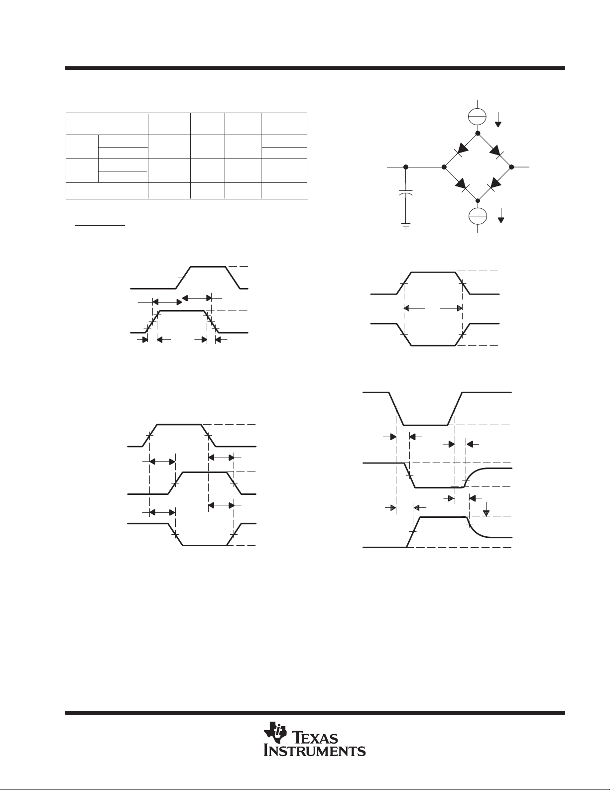
t
wH
2 V
0.8 V
t
r
t
c
Figure 2. PCLK Timing Waveform
PCLK
RSTIN
t
wL
t
2 V MIN Peak to Peak
f
t
w
PCLK
PCI Output
PCI Input
t
su
Figure 3. RSTIN Timing Waveforms
1.5 V
t
pd
1.5 V
Valid
t
on
Valid
t
su
t
pd
t
off
t
h
Figure 4. Shared-Signals Timing Waveforms
20
POST OFFICE BOX 655303 • DALLAS, TEXAS 75265
Page 21

PCI-TO-CARDBUS CONTROLLER UNIT
XCPS011 – DECEMBER 1997
PC Card cycle timing
The PC Card cycle timing is controlled by the wait-state bits in the Intel 82365SL-DF compatible memory and
I/O window registers. The PC Card cycle generator uses the PCI clock to generate the correct card address
setup and hold times and the PC Card command active (low) interval. This allows the cycle generator to output
PC Card cycles that are as close to the Intel 82365SL-DF timing as possible while always slightly exceeding
the Intel 82365SL-DF values. This ensures compatibility with existing software and maximizes throughput.
The PC Card address setup and hold times are a function of the wait-state bits. Table 1 shows address setup
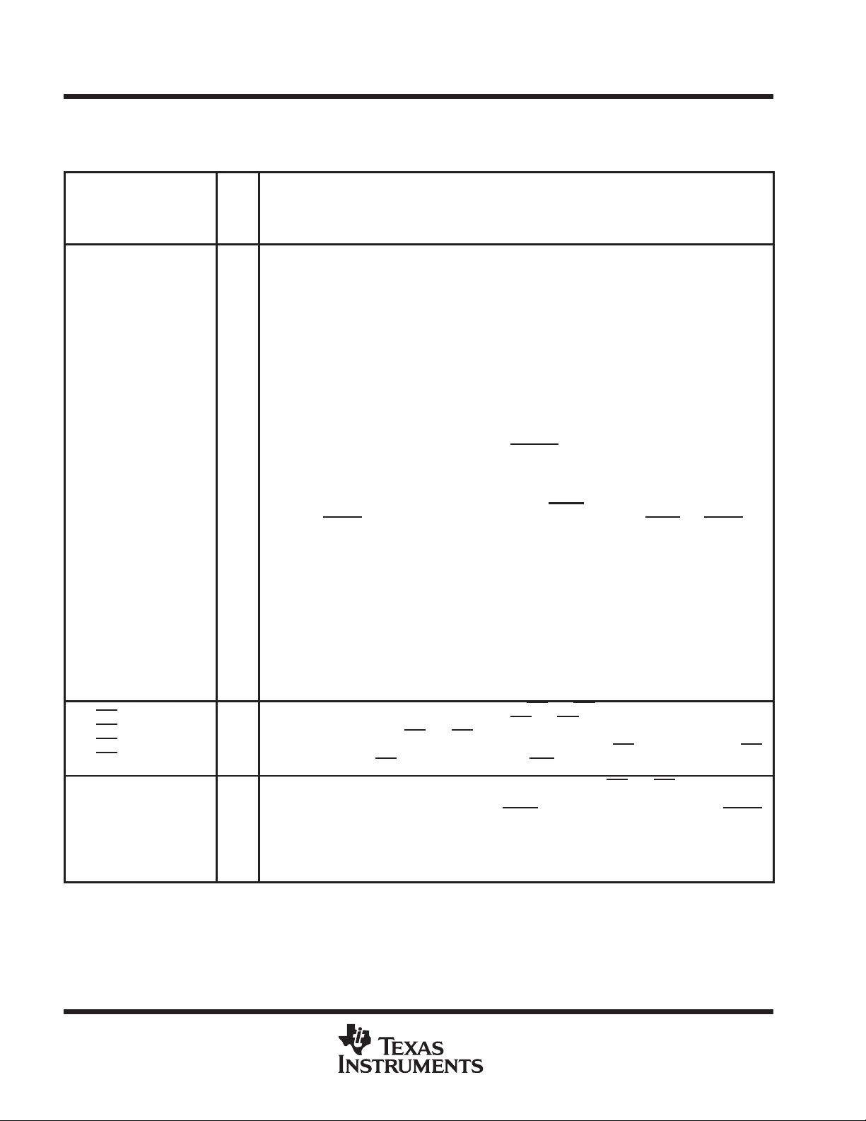
time in PCLK cycles and nanoseconds for I/O and memory cycles. Table 2 and Table 3 show command active
time in PCLK cycles and nanoseconds for I/O and memory cycles. Table 4 shows address hold time in PCLK
cycles and nanoseconds for I/O and memory cycles.
PCI1131
Table 1. PC Card Address Setup Time, t
WAIT-STATE BITS
I/O 3/90
Memory WS1 0 2/60
Memory WS1 1 4/120
Table 2. PC Card Command Active Time, t
WAIT-STATE BITS
WS ZWS
0 0 19/570
I/O
Memory
1 X 23/690
0 1 7/210
00 0 19/570
01 X 23/690
10 X 23/690
11 X 23/690
00 1 7/210
Table 3. PC Card Command Active Time, t
WAIT-STATE BITS
WS ZWS
0 0 7/210
I/O
Memory
1 X 11/330
0 1 N/A
00 0 9/270
01 X 13/390
10 X 17/510
11 X 23/630
00 1 5/150
, 8-Bit and 16-Bit PCI Cycles
su(A)
TS1 – 0 = 01
(PCLK/ns)
, 8-Bit PCI Cycles
c(A)
TS1 – 0 = 01
(PCLK/ns)
, 16-Bit PCI Cycles
c(A)
TS1 – 0 = 01
(PCLK/ns)
POST OFFICE BOX 655303 • DALLAS, TEXAS 75265
21
Page 22

PCI1131
PCI-TO-CARDBUS CONTROLLER UNIT
XCPS011 – DECEMBER 1997
Table 4. PC Card Address Hold Time, t
WAIT-STATE BITS
I/O 2/60
Memory WS1 0 2/60
Memory WS1 1 3/90
, 8-Bit and 16-Bit PCI Cycles
h(A)
TS1 – 0 = 01
(PCLK/ns)
timing requirements over recommended ranges of supply voltage and operating free-air
temperature, memory cycles (for 100-ns common memory) (see Note 5 and Figure 5)
ALTERNATE
SYMBOL
t
su
t
su
t
su
t
pd
t
w
t
h
t
h
t
su
t
h
t
h
t
su
t
h
NOTE 5: These times are dependent on the register settings associated with ISA wait states and data size. They are also dependent on cycle
Setup time, CE1 and CE2 before WE/OE low T1 60 ns
Setup time, CA25–CA0 before WE/OE low T2 t
Setup time, REG before WE/OE low T3 90 ns
Propagation delay time, WE/OE low to WAIT low T4 ns
Pulse duration, WE/OE low T5 200 ns
Hold time, WE/OE low after WAIT high T6 ns
Hold time, CE1 and CE2 after WE/OE high T7 120 ns
Setup time (read), CDATA15–CDATA0 valid before OE high T8 ns
Hold time (read), CDATA15–CDATA0 valid after OE high T9 0 ns
Hold time, CA25–CA0 and REG after WE/OE high T10 t
Setup time (write), CDATA15–CDATA0 valid before WE low T11 60 ns
Hold time (write), CDATA15–CDATA0 valid after WE low T12 240 ns
type (read/write, memory/I/O) and WAIT
observed if programmed for zero wait state, 16-bit cycles) with a 33-MHz PCI clock.
from PC Card. The times listed here represent absolute minimums (the times that would be
su(A)
h(A)
MIN MAX UNIT
+2PCLK ns
+1PCLK ns
timing requirements over recommended ranges of supply voltage and operating free-air
temperature, I/O cycles (see Figure 6)
ALTERNATE
SYMBOL
t
su
t
su
t
su
t
pd
t
pd
t
w
t
h
t
h
t
h
t
h
t
su
t
h
t
su
t
h
Setup time, REG before IORD/IOWR low T13 60 ns
Setup time, CE1 and CE2 before IORD/IOWR low T14 60 ns
Setup time, CA25–CA0 valid before IORD/IOWR low T15 t
Propagation delay time, IOIS16 low after CA25–CA0 valid T16 35 ns
Propagation delay time, IORD low to WAIT low T17 35 ns
Pulse duration, IORD/IOWR low T18 T
Hold time, IORD low after WAIT high T19 ns
Hold time, REG low after IORD high T20 0 ns
Hold time, CE1 and CE2 after IORD/IOWR high T21 120 ns
Hold time, CA25–CA0 after IORD/IOWR high T22 t
Setup time (read), CDATA15–CDATA0 valid before IORD high T23 10 ns
Hold time (read), CDATA15–CDATA0 valid after IORD high T24 0 ns
Setup time (write), CDATA15–CDATA0 valid before IOWR low T25 90 ns
Hold time (write), CDATA15–CDATA0 valid after IOWR high T26 90 ns
su(A)
h(A)
MIN MAX UNIT
+2PCLK ns
cA
+1PCLK ns
ns
22
POST OFFICE BOX 655303 • DALLAS, TEXAS 75265
Page 23

T27
tpdPropagation delay time
ns
T28
PCI1131
PCI-TO-CARDBUS CONTROLLER UNIT
XCPS011 – DECEMBER 1997
switching characteristics over recommended ranges of supply voltage and operating free-air
temperature, miscellaneous (see Figure 7)
ALTERNATE
SYMBOL
T10
MIN MAX UNIT
30
30
30
30
p
CA25–CA0
REG
PARAMETER
BVD2 low to SPKROUT low
BVD2 high to SPKROUT high
IREQ to IRQ15–IRQ3
STSCHG to IRQ15–IRQ3
PC Card PARAMETER MEASUREMENT INFORMATION
CE1, CE2
WE, OE
WAIT
CDATA15–CDATA0
(write)
CDATA15–CDATA0
(read)
With no wait state
With wait state
T2
T1
T3
T4
T11
T5
Figure 5. PC Card Memory Cycle
T7
T6
T12
T8
T9
POST OFFICE BOX 655303 • DALLAS, TEXAS 75265
23
Page 24

PCI1131
PCI-TO-CARDBUS CONTROLLER UNIT
XCPS011 – DECEMBER 1997
PC Card PARAMETER MEASUREMENT INFORMATION
CA25–CA0
T16
IOIS16
REG
CE1, CE2
T14
T18
T22
T20
T21
IORD, IOWR
WAIT
CDATA15–CDATA0
(write)
CDATA15–CDATA0
(read)
With no wait state
With wait state
T15
BVD2
SPKROUT
IREQ
T13
T17
T25
Figure 6. PC Card I/O Cycle
T27
T28
T19
T26
T23
T24
24
IRQ15–IRQ3
Figure 7. Miscellaneous PC Card Delay Times
POST OFFICE BOX 655303 • DALLAS, TEXAS 75265
Page 25

PCI1131
PCI-TO-CARDBUS CONTROLLER UNIT
XCPS011 – DECEMBER 1997
MECHANICAL DATA
PDV (S-PQFP-G208) PLASTIC QUAD FLATPACK
157
208
156
1
105
52
104
53
0,27
0,17
0,50
0,08
M
0,13 NOM
Gage Plane
25,50 TYP
28,05
SQ
27,95
30,10
SQ
29,90
1,45
1,35
1,60 MAX
NOTES: A. All linear dimensions are in millimeters.
B. This drawing is subject to change without notice.
C. Falls within JEDEC MO-136
0,05 MIN
0,25
0°–7°
0,75
0,45
Seating Plane
0,08
4087729/B 06/96
POST OFFICE BOX 655303 • DALLAS, TEXAS 75265
25
Page 26

IMPORTANT NOTICE
T exas Instruments and its subsidiaries (TI) reserve the right to make changes to their products or to discontinue
any product or service without notice, and advise customers to obtain the latest version of relevant information
to verify, before placing orders, that information being relied on is current and complete. All products are sold
subject to the terms and conditions of sale supplied at the time of order acknowledgement, including those
pertaining to warranty, patent infringement, and limitation of liability.
TI warrants performance of its semiconductor products to the specifications applicable at the time of sale in
accordance with TI’s standard warranty. Testing and other quality control techniques are utilized to the extent
TI deems necessary to support this warranty . Specific testing of all parameters of each device is not necessarily
performed, except those mandated by government requirements.
CERTAIN APPLICATIONS USING SEMICONDUCTOR PRODUCTS MAY INVOLVE POTENTIAL RISKS OF
DEATH, PERSONAL INJURY, OR SEVERE PROPERTY OR ENVIRONMENTAL DAMAGE (“CRITICAL
APPLICATIONS”). TI SEMICONDUCTOR PRODUCTS ARE NOT DESIGNED, AUTHORIZED, OR
WARRANTED TO BE SUITABLE FOR USE IN LIFE-SUPPORT DEVICES OR SYSTEMS OR OTHER
CRITICAL APPLICA TIONS. INCLUSION OF TI PRODUCTS IN SUCH APPLICATIONS IS UNDERST OOD TO
BE FULLY AT THE CUSTOMER’S RISK.
In order to minimize risks associated with the customer’s applications, adequate design and operating
safeguards must be provided by the customer to minimize inherent or procedural hazards.
TI assumes no liability for applications assistance or customer product design. TI does not warrant or represent
that any license, either express or implied, is granted under any patent right, copyright, mask work right, or other
intellectual property right of TI covering or relating to any combination, machine, or process in which such
semiconductor products or services might be or are used. TI’s publication of information regarding any third
party’s products or services does not constitute TI’s approval, warranty or endorsement thereof.
Copyright 1998, Texas Instruments Incorporated
 Loading...