

Page 1
PCA9546A
4-CHANNEL I2C AND SMBus SWITCH
www.ti.com
1
FEATURES
SCPS148E – OCTOBER 2005 – REVISED JANUARY 2008
• 1-of-4 Bidirectional Translating Switches • Low Standby Current
• I2C Bus and SMBus Compatible • Operating Power-Supply Voltage Range of
• Active-Low Reset Input
• Three Address Pins, Allowing up to Eight
2.3 V to 5.5 V
• 5.5-V Tolerant Inputs
Devices on the I2C Bus • 0 to 400-kHz Clock Frequency
• Channel Selection Via I2C Bus • Latch-Up Performance Exceeds 100 mA Per
• Power Up With All Switch Channels
JESD 78
Deselected • ESD Protection Exceeds JESD 22
• Low R
Switches – 2000-V Human-Body Model (A114-A)
ON
• Allows Voltage-Level Translation Between – 200-V Machine Model (A115-A)
1.8-V, 2.5-V, 3.3-V, and 5-V Buses
– 1000-V Charged-Device Model (C101)
• No Glitch on Power Up
• Supports Hot Insertion
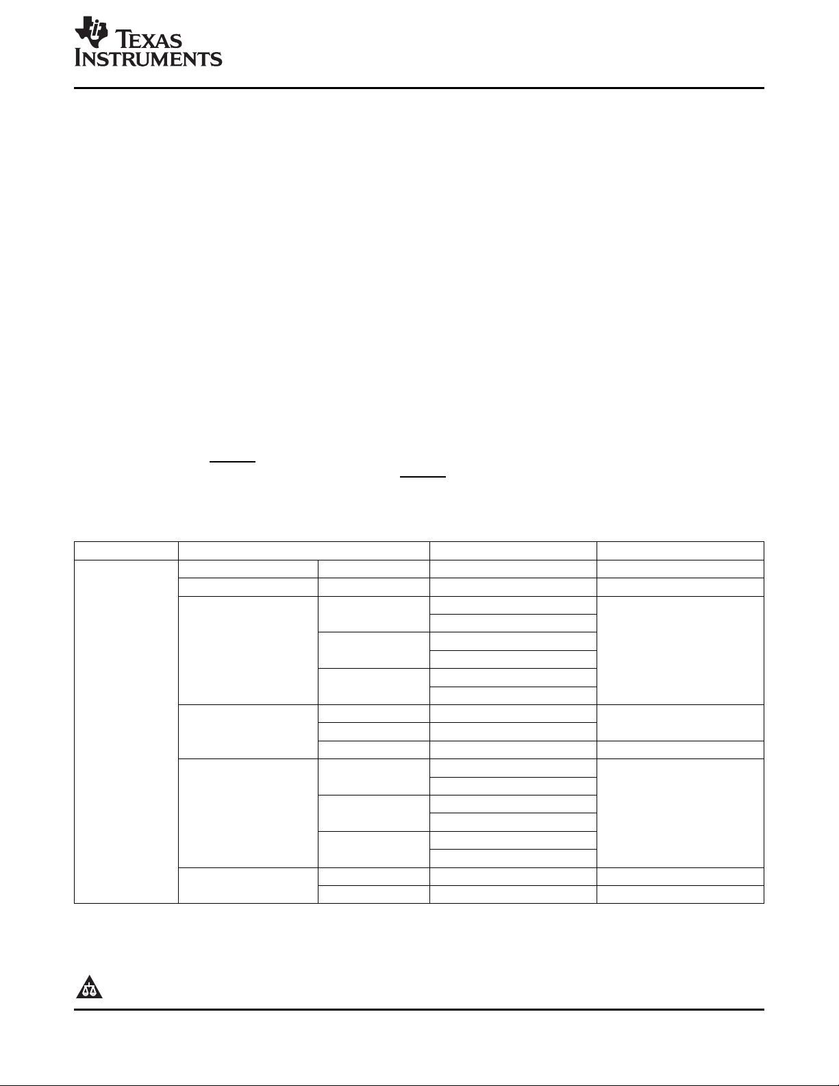
DESCRIPTION/ORDERING INFORMATION
The PCA9546A is a quad bidirectional translating switch controlled via the I2C bus. The SCL/SDA upstream pair
fans out to four downstream pairs, or channels. Any individual SCn/SDn channel or combination of channels can
be selected, determined by the contents of the programmable control register.
An active-low reset ( RESET) input allows the PCA9546A to recover from a situation in which one of the
downstream I2C buses is stuck in a low state. Pulling RESET low resets the I2C state machine and causes all the
channels to be deselected, as does the internal power-on reset function.
WITH RESET FUNCTION
ORDERING INFORMATION
T
A
QFN – RGV Reel of 2500 PCA9546ARGVR PD546A
QFN – RGY Reel of 1000 PCA9546ARGYR PD546A
SOIC – D Reel of 2500 PCA9546A
– 40 ° C to 85 ° C SOIC – DW Reel of 2000 PCA9546ADWR
TSSOP – PW Reel of 2000 PD546A
TVSOP – DGV
(1) For the most current package and ordering information, see the Package Option Addendum at the end of this document, or see the TI
website at www.ti.com .
(2) Package drawings, thermal data, and symbolization are available at www.ti.com/packaging .
PACKAGE
(1) (2)
Tube of 40
Reel of 250
Tube of 40 PCA9546ADW
Reel of 250 PCA9546ADWT PREVIEW
Tube of 90
Reel of 250
Reel of 2000 PCA9546ADGVR PD546A
Reel of 250 PCA9546ADGVT PREVIEW
ORDERABLE PART NUMBER TOP-SIDE MARKING
PCA9546AD
PCA9546ADG4
PCA9546ADR
PCA9546ADRG4
PCA9546ADT
PCA9546ADTG4
PCA9546APW
PCA9546APWE4
PCA9546APWR
PCA9546APWRE4
PCA9546APWT
PCA9546APWTE4
PCA9546A
1
Please be aware that an important notice concerning availability, standard warranty, and use in critical applications of
Texas Instruments semiconductor products and disclaimers thereto appears at the end of this data sheet.
PRODUCTION DATA information is current as of publication date.
Products conform to specifications per the terms of the Texas
Instruments standard warranty. Production processing does not
necessarily include testing of all parameters.
Copyright © 2005 – 2008, Texas Instruments Incorporated
Page 2
www.ti.com
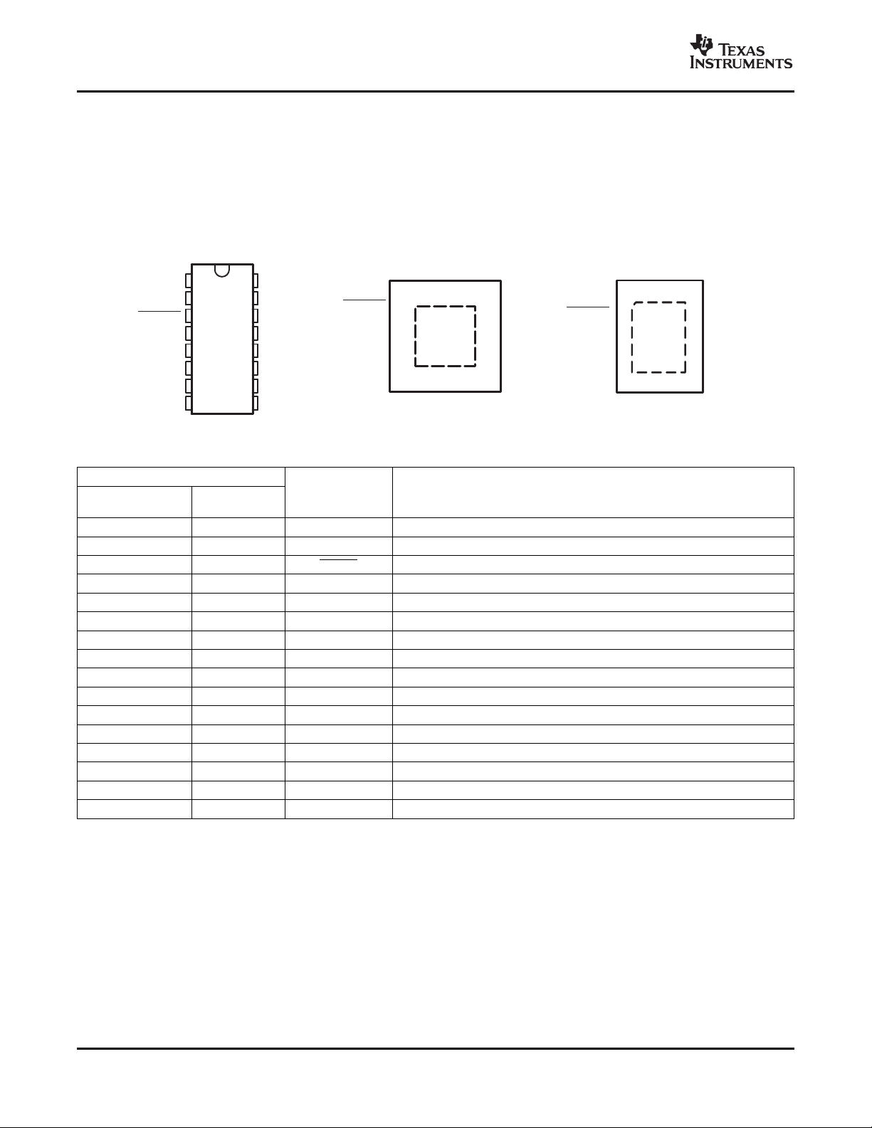
D, DGV, DW, OR PW PACKAGE
(TOP VIEW)
1
2
3
4
5
6
7
8
16
15
14
13
12
11
10
9
A0
A1
RESET
SD0
SC0
SD1
SC1
GND
V
CC
SDA
SCL
A2
SC3
SD3
SC2
SD2
RGY PACKAGE
(TOP VIEW)
2
15
SDAA1
3
14
SCL
RESET
4
13
A2SD0
5
12
SC3SC0
6
11
SD3SD1
7
10
SC2SC1
1
8
A0
GND
16
9
SD2
V
CC
RGV PACKAGE
(TOP VIEW)
8
SC2
13
SD
A
16
5
A1
SC1
6
15
A0
GND
V
CC
7
14
SD2
1 12
SCL
RESET
2 11
A2SD0
10
SC3
3
SC0
4
9
SD3SD1
PCA9546A
4-CHANNEL I2C AND SMBus SWITCH
WITH RESET FUNCTION
SCPS148E – OCTOBER 2005 – REVISED JANUARY 2008
DESCRIPTION/ORDERING INFORMATION (CONTINUED)
The pass gates of the switches are constructed such that the V
voltage, which will be passed by the PCA9546A. This allows the use of different bus voltages on each pair, so
that 1.8-V, 2.5-V, or 3.3-V parts can communicate with 5-V parts without any additional protection. External
pullup resistors pull the bus up to the desired voltage level for each channel. All I/O pins are 5.5-V tolerant.
pin can be used to limit the maximum high
CC
TERMINAL FUNCTIONS
NO.
D, DGV, DW, PW,
AND RGY
1 15 A0 Address input 0. Connect directly to V
2 16 A1 Address input 1. Connect directly to V
3 1 RESET Active low reset input. Connect to V
4 2 SD0 Serial data 0. Connect to V
5 3 SC0 Serial clock 0. Connect to V
6 4 SD1 Serial data 1. Connect to V
7 5 SC1 Serial clock 1. Connect to V
8 6 GND Ground
9 7 SD2 Serial data 2. Connect to V
10 8 SC2 Serial clock 2. Connect to V
11 9 SD3 Serial data 3. Connect to V
12 10 SC3 Serial clock 3. Connect to V
13 11 A2 Address input 2. Connect directly to V
14 12 SCL Serial clock line. Connect to V
15 13 SDA Serial data line. Connect to V
16 14 V
RGV
NAME DESCRIPTION
CC
Supply power
through a pullup resistor.
CC
CC
through a pullup resistor.
CC
CC
through a pullup resistor.
CC
CC
through a pullup resistor.
CC
CC
CC
CC
or ground.
CC
or ground.
CC
through a pullup resistor, if not used.
CC
through a pullup resistor.
through a pullup resistor.
through a pullup resistor.
through a pullup resistor.
or ground.
CC
through a pullup resistor.
through a pullup resistor.
2 Submit Documentation Feedback Copyright © 2005 – 2008, Texas Instruments Incorporated
Product Folder Link(s): PCA9546A
Page 3
www.ti.com
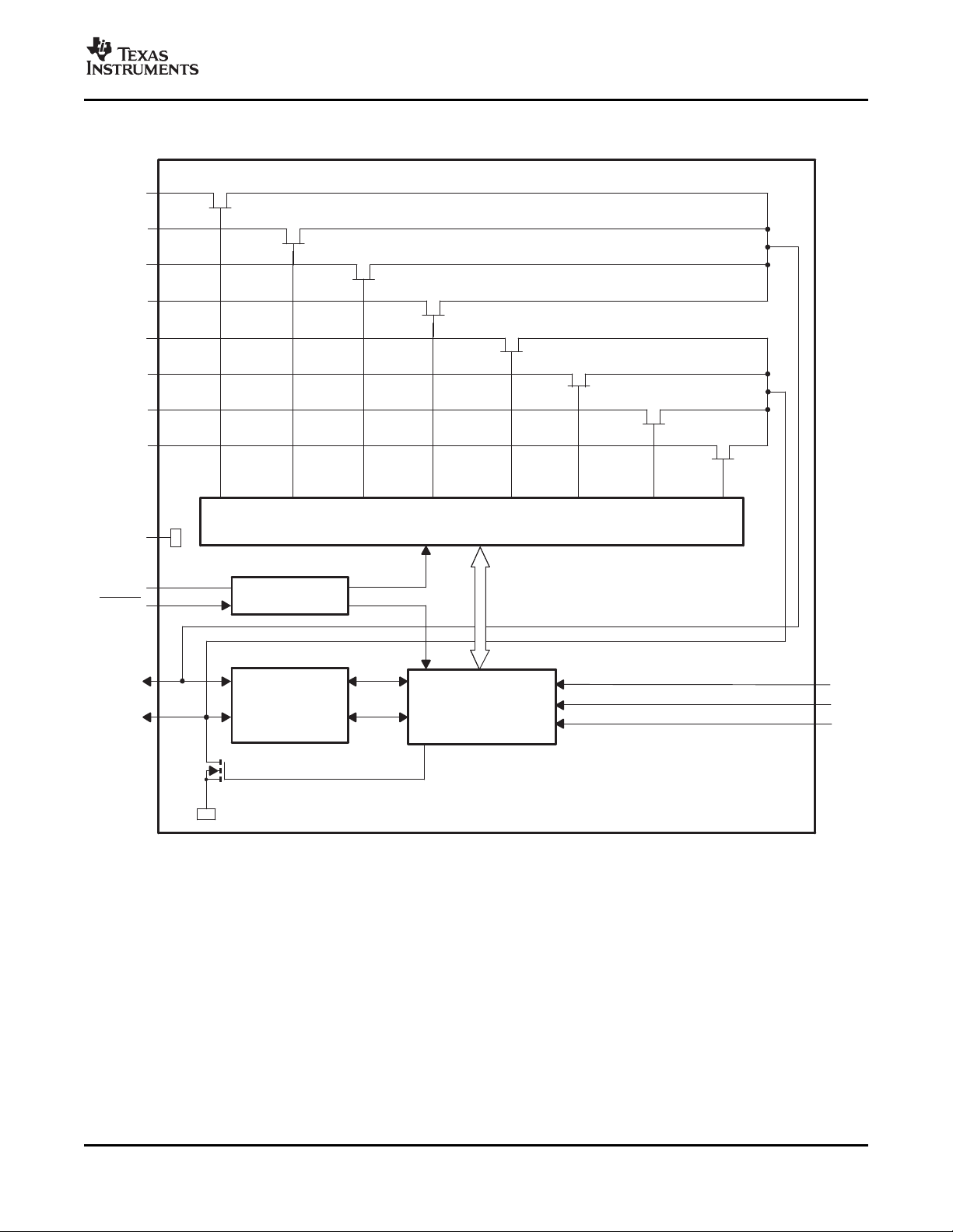
Switch Control Logic
I2C Bus Control
Input Filter
Power-On Reset
PCA9546A
SC0
SDA
SCL
RESET
GND
SD3
SD2
SD1
SD0
SC3
SC2
SC1
V
CC
A1
A0
A2
5
14
3
16
8
11
9
6
4
12
10
7
15
1
2
13
PCA9546A
4-CHANNEL I2C AND SMBus SWITCH
WITH RESET FUNCTION
SCPS148E – OCTOBER 2005 – REVISED JANUARY 2008
BLOCK DIAGRAM
A. Pin numbers shown are for the D, DGV, DW, PW and RGY packages.
Copyright © 2005 – 2008, Texas Instruments Incorporated Submit Documentation Feedback 3
Product Folder Link(s): PCA9546A
Page 4
www.ti.com
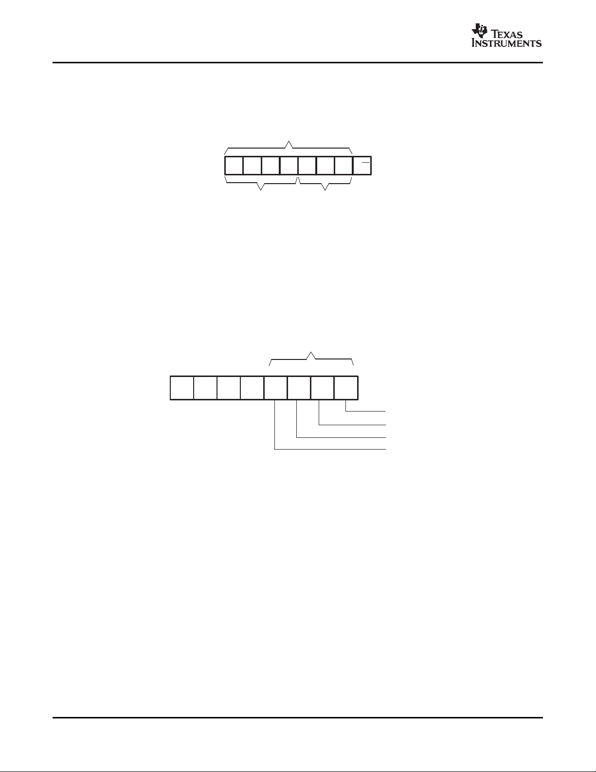
1 1 1
0
A1A2
A0
Slave Address
R/W
Fixed
Hardware
Selectable
Channel Selection Bits
(Read/Write)
Channel 0
Channel 1
Channel 2
Channel 3
B3 B2 B1 B0
3 2 1 0
XXXX
4567
PCA9546A
4-CHANNEL I2C AND SMBus SWITCH
WITH RESET FUNCTION
SCPS148E – OCTOBER 2005 – REVISED JANUARY 2008
Device Address
Following a start condition, the bus master must output the address of the slave it is accessing. The address of
the PCA9546A is shown in Figure 1 . To conserve power, no internal pullup resistors are incorporated on the
hardware-selectable address pins, and they must be pulled high or low.
Figure 1. PCA9546A Address
The last bit of the slave address defines the operation to be performed. When set to a logic 1, a read is selected,
while a logic 0 selects a write operation.
Control Register
Following the successful acknowledgment of the slave address, the bus master sends a byte to the PCA9546A,
which is stored in the control register (see Figure 2 ). If multiple bytes are received by the PCA9546A, it will save
the last byte received. This register can be written and read via the I2C bus.
Figure 2. Control Register
Control Register Definition
One or several SCn/SDn downstream pairs, or channels, are selected by the contents of the control register (see
Table 1 ). This register is written after the PCA9546A has been addressed. The four LSBs of the control byte are
used to determine which channel or channels are to be selected. When a channel is selected, the channel
becomes active after a stop condition has been placed on the I2C bus. This ensures that all SCn/SDn lines are in
a high state when the channel is made active, so that no false conditions are generated at the time of
connection. A stop condition always must occur right after the acknowledge cycle.
4 Submit Documentation Feedback Copyright © 2005 – 2008, Texas Instruments Incorporated
Product Folder Link(s): PCA9546A
Page 5
www.ti.com
2
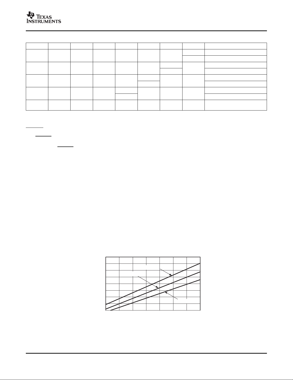
Maximum
Typical
Minimum
VCC (V)
4.543.532.5 5 5.5
1
5
4.5
4
3.5
3
2.5
2
1.5
V
pass
(V)
PCA9546A
4-CHANNEL I2C AND SMBus SWITCH
WITH RESET FUNCTION
SCPS148E – OCTOBER 2005 – REVISED JANUARY 2008
Table 1. Control Register Write (Channel Selection), Control Register Read (Channel Status)
B7 B6 B5 B4 B3 B2 B1 B0 COMMAND
X X X X X X X
X X X X X X X
X X X X X X X
X X X X X X X
0 0 0 0 0 0 0 0
(1) Several channels can be enabled at the same time. For example, B3 =0, B2 = 1, B1 = 1, B0 = 0 means that channels 0 and 3 are
disabled, and channels 1 and 2 are enabled. Care should be taken not to exceed the maximum bus capacity.
0 Channel 3 disabled
1 Channel 3 enabled
0 Channel 2 disabled
1 Channel 2 enabled
0 Channel 1 disabled
1 Channel 1 enabled
0 Channel 0 disabled
1 Channel 0 enabled
No channel selected,
power-up/reset default state
RESET Input
The RESET input is an active-low signal that may be used to recover from a bus-fault condition. When this signal
is asserted low for a minimum of tWL, the PCA9446A resets its registers and I2C state machine and deselects all
channels. The RESET input must be connected to V
through a pullup resistor.
CC
(1)
Power-On Reset
When power is applied to V
reached V
. At this point, the reset condition is released, and the PCA9546A registers and I2C state machine
POR
are initialized to their default states, all zeroes, causing all the channels to be deselected. Thereafter, V
be lowered below 0.2 V to reset the device.
, an internal power-on reset holds the PCA9546A in a reset condition until V
CC
CC
CC
Voltage Translation
The pass-gate transistors of the PCA9546A are constructed such that the V
maximum voltage that will be passed from one I2C bus to another.
Figure 3 shows the voltage characteristics of the pass-gate transistors (note that the graph was generated using
the data specified in the electrical characteristics section of this data sheet). In order for the PCA9546A to act as
a voltage translator, the V
voltage must be equal to or lower than the lowest bus voltage. For example, if the
pass
main bus is running at 5 V, and the downstream buses are 3.3 V and 2.7 V, then V
2.7 V to effectively clamp the downstream bus voltages. As shown in Figure 3 , V
PCA9546A supply voltage is 3.5 V or lower, so the PCA9546A supply voltage could be set to 3.3 V. Pullup
resistors then can be used to bring the bus voltages to their appropriate levels (see Figure 12 ).
voltage can be used to limit the
CC
must be equal to or below
pass
(max) is at 2.7 V when the
pass
has
must
Copyright © 2005 – 2008, Texas Instruments Incorporated Submit Documentation Feedback 5
Figure 3. V
Product Folder Link(s): PCA9546A
Voltage vs V
pass
CC
Page 6
www.ti.com
SDA
SCL
Data Line
Stable;
Data Valid
Change
of Data
Allowed
SDA
SCL
Start Condition
S
Stop Condition
P
SCL
Master
Transmitter/
Receiver
Slave
Receiver
Slave
Transmitter/
Receiver
Master
Transmitter
Master
Transmitter/
Receiver
I2C
Multiplexer
Slave
SDA
PCA9546A
4-CHANNEL I2C AND SMBus SWITCH
WITH RESET FUNCTION
SCPS148E – OCTOBER 2005 – REVISED JANUARY 2008
I2C Interface
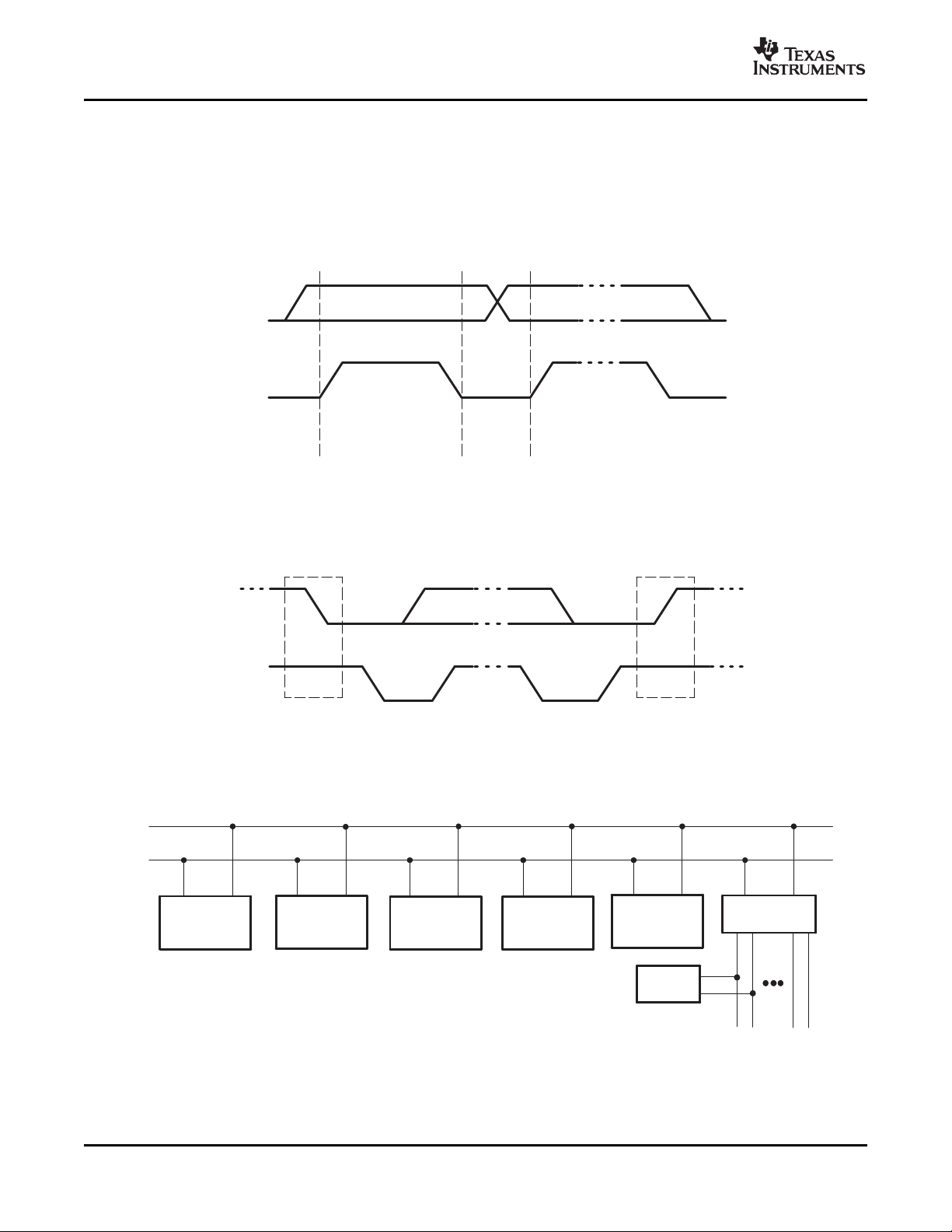
The I2C bus is for two-way two-line communication between different ICs or modules. The two lines are a serial
data line (SDA) and a serial clock line (SCL). Both lines must be connected to a positive supply via a pullup
resistor when connected to the output stages of a device. Data transfer can be initiated only when the bus is not
busy.
One data bit is transferred during each clock pulse. The data on the SDA line must remain stable during the high
period of the clock pulse, as changes in the data line at this time are interpreted as control signals (see Figure 4 ).
Figure 4. Bit Transfer
Both data and clock lines remain high when the bus is not busy. A high-to-low transition of the data line while the
clock is high is defined as the start condition (S). A low-to-high transition of the data line while the clock is high is
defined as the stop condition (P) (see Figure 5 ).
Figure 5. Definition of Start and Stop Conditions
A device generating a message is a transmitter; a device receiving is the receiver. The device that controls the
message is the master, and the devices that are controlled by the master are the slaves (see Figure 6 ).
Figure 6. System Configuration
The number of data bytes transferred between the start and the stop conditions from transmitter to receiver is not
limited. Each byte of eight bits is followed by one acknowledge (ACK) bit. The transmitter must release the SDA
line before the receiver can send an ACK bit.
6 Submit Documentation Feedback Copyright © 2005 – 2008, Texas Instruments Incorporated
Product Folder Link(s): PCA9546A
Page 7
www.ti.com
Data Output
by Transmitter
SCL From
Master
Start
Condition
S
1 2 8 9
Data Output
by Receiver
Clock Pulse for ACK
NACK
ACK
A AS 1 1 1 0 A2 A1 A0 0
Start Condition
SDA
R/W ACK From Slave ACK From Slave
P
B0B1B2B3XXXX
Stop Condition
Slave Address
Control Register
A
NA
S 1 1 1
0 A2 A1 A0
1
SDA
P
B3 B2 B1 B0
Start Condition R/W ACK From Slave NACK From Master Stop Condition
Slave Address Control Register
0 0 0 0
PCA9546A
4-CHANNEL I2C AND SMBus SWITCH
WITH RESET FUNCTION
SCPS148E – OCTOBER 2005 – REVISED JANUARY 2008
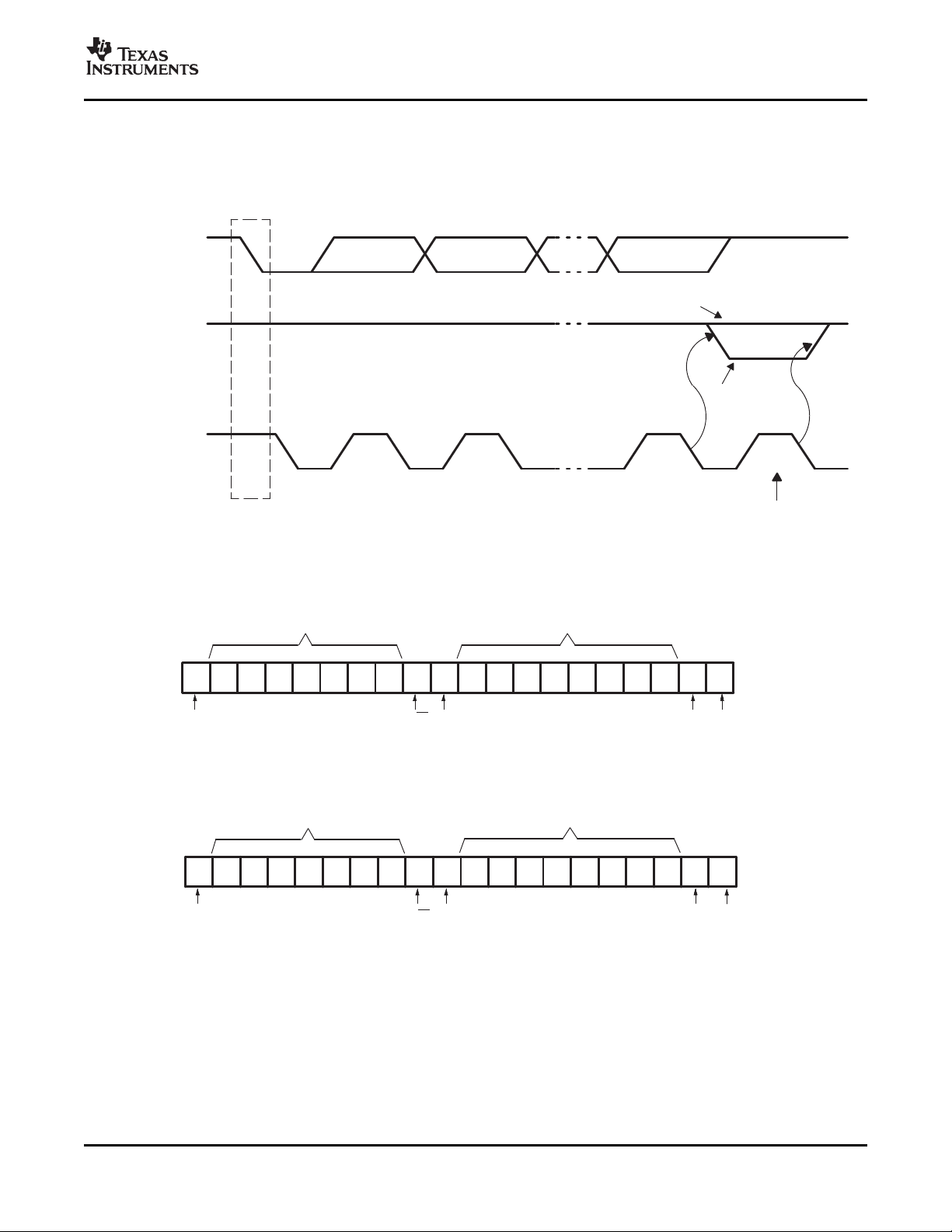
When a slave receiver is addressed, it must generate an ACK after the reception of each byte. Also, a master
must generate an ACK after the reception of each byte that has been clocked out of the slave transmitter. The
device that acknowledges must pull down the SDA line during the ACK clock pulse so that the SDA line is stable
low during the high pulse of the ACK-related clock period (see Figure 7 ). Setup and hold times must be taken
into account.
Figure 7. Acknowledgment on the I2C Bus
Data is transmitted to the PCA9546A control register using the write mode shown in Figure 8 .
Figure 8. Write Control Register
Data is read from the PCA9546A control register using the read mode shown in Figure 9 .
Figure 9. Read Control Register
Copyright © 2005 – 2008, Texas Instruments Incorporated Submit Documentation Feedback 7
Product Folder Link(s): PCA9546A
Page 8
www.ti.com
PCA9546A
4-CHANNEL I2C AND SMBus SWITCH
WITH RESET FUNCTION
SCPS148E – OCTOBER 2005 – REVISED JANUARY 2008
Absolute Maximum Ratings
(1)
over operating free-air temperature range (unless otherwise noted)
MIN MAX UNIT
V
V
I
I
I
O
θ
JA
P
T
T
(1) Stresses beyond those listed under "absolute maximum ratings" may cause permanent damage to the device. These are stress ratings
(2) The input negative-voltage and output voltage ratings may be exceeded if the input and output current ratings are observed.
(3) The package thermal impedance is calculated in accordance with JESD 51-7.
Supply voltage range – 0.5 7 V
CC
Input voltage range
I
(2)
Input current ± 20 mA
Output current ± 25 mA
Continuous current through V
CC
Continuous current through GND ± 100 mA
D package 73
DGV package 120
Package thermal impedance
(3)
DW package 57
PW package 108
RGV package 51.38
RGY package 50
Total power dissipation 400 mW
tot
Storage temperature range – 65 150 ° C
stg
Operating free-air temperature range – 40 85 ° C
A
only, and functional operation of the device at these or any other conditions beyond those indicated under "recommended operating
conditions" is not implied. Exposure to absolute-maximum-rated conditions for extended periods may affect device reliability.
– 0.5 7 V
± 100 mA
° C/W
Recommended Operating Conditions
V
V
V
T
(1) All unused inputs of the device must be held at V
Supply voltage 2.3 5.5 V
CC
High-level input voltage V
IH
Low-level input voltage V
IL
Operating free-air temperature – 40 85 ° C
A
Implications of Slow or Floating CMOS Inputs, literature number SCBA004.
(1)
MIN MAX UNIT
SCL, SDA 0.7 × V
A2 – A0, RESET 0.7 × V
CC
V
CC
CC
SCL, SDA – 0.5 0.3 × V
A2 – A0, RESET – 0.5 0.3 × V
or GND to ensure proper device operation. Refer to the TI application report,
CC
6
+ 0.5
CC
CC
8 Submit Documentation Feedback Copyright © 2005 – 2008, Texas Instruments Incorporated
Product Folder Link(s): PCA9546A
Page 9
www.ti.com
Electrical Characteristics
over recommended operating free-air temperature range (unless otherwise noted)
PARAMETER TEST CONDITIONS V
V
POR
V
pass
I
OL
Power-on reset voltage
Switch output voltage V
SCL, SDA 2.3 V to 5.5 V mA
SCL, SDA ± 1
I
I
SC3 – SC0, SD3 – SD0 ± 1
A2 – A0 ± 1
RESET ± 1
Operating mode f
I
CC
Standby mode
Δ I
CC
C
i
C
io(OFF)
R
ON
Supply-current
change
A2 – A0 4.5 6
RESET 4.5 5.5
SCL, SDA 15 19
(3)
SC3 – SC0, SD3 – SD0 6 8
Switch on-state resistance 3 V to 3.6 V 5 11 20 Ω
(1) All typical values are at nominal supply voltage (2.5-V, 3.3-V, or 5-V VCC), TA= 25 ° C.
(2) The power-on reset circuit resets the I2C bus logic with V
(3) C
depends on internal capacitance and external capacitance added to the SCn lines when channels(s) are ON.
io(ON)
(2)
= 100 kHz VI= V
SCL
No load, VI= V
= VCC, I
SWin
V
= 0.4 V 3 7
OL
V
= 0.6 V 6 10
OL
VI= V
or GND 2.3 V to 5.5 V µ A
CC
or GND, IO= 0 3.6 V 3 11
CC
SWout
or GND V
CC
= – 100 µ A V
Low inputs VI= GND, IO= 0 3.6 V 0.1 1 µ A
High inputs VI= VCC, IO= 0 3.6 V 0.1 1
SCL or SDA input at 0.6 V,
SCL, SDA µ A
Other inputs at V
SCL or SDA input at V
Other inputs at V
VI= V
VI= V
or GND 2.3 V to 5.5 V pF
CC
or GND, Switch OFF 2.3 V to 5.5 V pF
CC
or GND
CC
– 0.6 V,
CC
or GND
CC
VO= 0.4 V, IO= 15 mA
VO= 0.4 V, IO= 10 mA 2.3 V to 2.7 V 7 16 45
< V
. V
CC
POR
must be lowered to 0.2 V to reset the device.
CC
4-CHANNEL I2C AND SMBus SWITCH
WITH RESET FUNCTION
SCPS148E – OCTOBER 2005 – REVISED JANUARY 2008
CC
POR
5 V 3.6
4.5 V to 5.5 V 2.6 4.5
3.3 V 1.9
3 V to 3.6 V 1.6 2.8
2.5 V 1.5
2.3 V to 2.7 V 1.1 2
5.5 V 3 12
2.7 V 3 10
5.5 V 0.3 1
2.7 V 0.1 1
5.5 V 0.3 1
2.7 V 0.1 1
2.3 V to 5.5 V 8 15
4.5 V to 5.5 V 4 9 16
MIN TYP
PCA9546A
(1)
MAX UNIT
1.6 2.1 V
8 15
Copyright © 2005 – 2008, Texas Instruments Incorporated Submit Documentation Feedback 9
Product Folder Link(s): PCA9546A
Page 10

www.ti.com
PCA9546A
4-CHANNEL I2C AND SMBus SWITCH
WITH RESET FUNCTION
SCPS148E – OCTOBER 2005 – REVISED JANUARY 2008
I2C Interface Timing Requirements
over recommended operating free-air temperature range (unless otherwise noted) (see Figure 10 )
STANDARD MODE FAST MODE
I2C BUS I2C BUS
MIN MAX MIN MAX
f
scl
t
sch
t
scl
t
sp
t
sds
t
sdh
t
icr
t
icf
t
ocf
t
buf
t
sts
t
sth
t
sps
t
vdL(Data)
t
vdH(Data)
t
vd(ack)
C
b
(1) A device internally must provide a hold time of at least 300 ns for the SDA signal (referred to the VIHmin of the SCL signal), in order to
(2) Cb= total bus capacitance of one bus line in pF
(3) Data taken using a 1-k Ω pullup resistor and 50-pF load (see Figure 10 )
I2C clock frequency 0 100 0 400 kHz
I2C clock high time 4 0.6 µ s
I2C clock low time 4.7 1.3 µ s
I2C spike time 50 50 ns
I2C serial-data setup time 250 100 ns
I2C serial-data hold time 0
I2C input rise time 1000 20 + 0.1C
I2C input fall time 300 20 + 0.1C
I2C output fall time 10-pF to 400-pF bus 300 20 + 0.1C
(1)
0
b
b
b
I2C bus free time between stop and start 4.7 1.3 µ s
I2C start or repeated start condition setup 4.7 0.6 µ s
I2C start or repeated start condition hold 4 0.6 µ s
I2C stop condition setup 4 0.6 µ s
Valid-data time (high to low)
Valid-data time (low to high)
Valid-data time of ACK condition 1 1 µ s
(3)
SCL low to SDA output low valid 1 1 µ s
(3)
SCL low to SDA output high valid 0.6 0.6 µ s
ACK signal from SCL low
to SDA output low
I2C bus capacitive load 400 400 pF
bridge the undefined region of the falling edge of SCL.
(1)
(2)
300 ns
(2)
300 ns
(2)
300 ns
UNIT
µ s
Switching Characteristics
over recommended operating free-air temperature range, CL≤ 100 pF (unless otherwise noted) (see Figure 10 )
PARAMETER MIN MAX UNIT
R
= 20 Ω , CL= 15 pF 0.3
(1)
t
Propagation delay time SDA or SCL SDn or SCn ns
pd
ON
R
= 20 Ω , CL= 50 pF 1
ON
(1) The propagation delay is the calculated RC time constant of the typical ON-state resistance of the switch and the specified load
capacitance, when driven by an ideal voltage source (zero output impedance).
FROM TO
(INPUT) (OUTPUT)
Interrupt and Reset Timing Requirements
over recommended operating free-air temperature range (unless otherwise noted)
PARAMETER MIN MAX UNIT
t
WL
(1)
t
rst
t
REC(STA)
(1) t
signaling a stop condition. It must be a minimum of tWL.
Pulse duration, RESET low 6 ns
RESET time (SDA clear) 500 ns
Recovery time from RESET to start 0 ns
is the propagation delay measured from the time the RESET pin is first asserted low to the time the SDA pin is asserted high,
rst
10 Submit Documentation Feedback Copyright © 2005 – 2008, Texas Instruments Incorporated
Product Folder Link(s): PCA9546A
Page 11

www.ti.com
PARAMETER MEASUREMENT INFORMATION
RL = 1 kΩ
V
CC
CL = 50 pF
(See Note A)
t
buf
t
icr
t
sth
t
sds
t
sdh
t
icf
t
icr
t
scl
t
sch
t
sts
t
vd(ACK)
or t
vdL
t
vdH
0.3 × V
CC
Stop
Condition
t
sps
Repeat
Start
Condition
Start or Repeat
Start Condition
SCL
SDA
Start
Condition
(S)
Address
Bit 7
(MSB)
Data
Bit 0
(LSB)
Stop
Condition
(P)
Two Bytes for Complete
Device Programming
I2C PORT LOAD CONFIGURATION
VOLTAGE WAVEFORMS
t
icf
Stop
Condition
(P)
t
sp
DUT
SDn, SCn
0.7 × V
CC
0.3 × V
CC
0.7 × V
CC
R/W
Bit 0
(LSB)
ACK
(A)
Data
Bit 7
(MSB)
Address
Bit 1
Address
Bit 6
ACK
(A)
BYTE DESCRIPTION
I2C address + R/W
Control register data
1
2
PCA9546A
4-CHANNEL I2C AND SMBus SWITCH
WITH RESET FUNCTION
SCPS148E – OCTOBER 2005 – REVISED JANUARY 2008
A. CLincludes probe and jig capacitance.
B. All input pulses are supplied by generators having the following characteristics: PRR ≤ 10 MHz, ZO= 50 Ω ,
C. The outputs are measured one at a time, with one transition per measurement.
Copyright © 2005 – 2008, Texas Instruments Incorporated Submit Documentation Feedback 11
tr/tf≤ 30 ns.
Figure 10. I2C Interface Load Circuit, Byte Descriptions, and Voltage Waveforms
Product Folder Link(s): PCA9546A
Page 12

www.ti.com
SCL
SDA
LEDx
RESET
30%
50%
50%
LED OFF
ACK or Read CycleStart
t
REC
t
WL
t
rst
t
rst
PCA9546A
4-CHANNEL I2C AND SMBus SWITCH
WITH RESET FUNCTION
SCPS148E – OCTOBER 2005 – REVISED JANUARY 2008
PARAMETER MEASUREMENT INFORMATION (continued)
Figure 11. Reset Timing
12 Submit Documentation Feedback Copyright © 2005 – 2008, Texas Instruments Incorporated
Product Folder Link(s): PCA9546A
Page 13

www.ti.com
APPLICATION INFORMATION
PCA9546A
SD1
SDA
Channel 0
Channel 1
Channel 2
Channel 3
See Note A
I2C/SMBus
Master
SCL
RESET
SC1
SD2
SC2
SD3
SC3
SD0
SC0
VCC = 2.7 V to 5.5 V
VCC = 3.3 V
VCC = 2.7 V to 5.5 V
VCC = 2.7 V to 5.5 V
VCC = 2.7 V to 5.5 V
VCC = 2.7 V to 5.5 V
See Note A
See Note A
See Note A
SDA
SCL
A2
A1
A0
GND
15
14
3
8
1
2
13
16
12
11
10
9
7
6
5
4
Figure 12 shows an application in which the PCA9546A can be used.
PCA9546A
4-CHANNEL I2C AND SMBus SWITCH
WITH RESET FUNCTION
SCPS148E – OCTOBER 2005 – REVISED JANUARY 2008
A. Pin numbers shown are for the D, DGV, DW, PW, and RGY packages.
Figure 12. Typical Application
Copyright © 2005 – 2008, Texas Instruments Incorporated Submit Documentation Feedback 13
Product Folder Link(s): PCA9546A
Page 14

PACKAGE OPTION ADDENDUM
www.ti.com
PACKAGING INFORMATION
Orderable Device Status
PCA9546AD ACTIVE SOIC D 16 40 Green (RoHS &
PCA9546ADG4 ACTIVE SOIC D 16 40 Green (RoHS &
PCA9546ADGVR ACTIVE TVSOP DGV 16 2000 Green (RoHS &
PCA9546ADGVRG4 ACTIVE TVSOP DGV 16 2000 Green (RoHS &
PCA9546ADGVT PREVIEW TVSOP DGV 20 250 TBD Call TI Call TI
PCA9546ADR ACTIVE SOIC D 16 2500 Green (RoHS &
PCA9546ADRG4 ACTIVE SOIC D 16 2500 Green (RoHS &
PCA9546ADT ACTIVE SOIC D 16 250 Green (RoHS &
PCA9546ADTG4 ACTIVE SOIC D 16 250 Green (RoHS &
PCA9546ADW ACTIVE SOIC DW 16 40 Green (RoHS &
PCA9546ADWG4 ACTIVE SOIC DW 16 40 Green (RoHS &
PCA9546ADWR ACTIVE SOIC DW 16 2000 Green (RoHS &
PCA9546ADWRG4 ACTIVE SOIC DW 16 2000 Green (RoHS &
PCA9546ADWT PREVIEW SOIC DW 16 250 TBD Call TI Call TI
PCA9546AGQNR PREVIEW BGA MI
PCA9546APW ACTIVE TSSOP PW 16 90 Green (RoHS &
PCA9546APWE4 ACTIVE TSSOP PW 16 90 Green (RoHS &
PCA9546APWG4 ACTIVE TSSOP PW 16 90 Green (RoHS &
PCA9546APWR ACTIVE TSSOP PW 16 2000 Green (RoHS &
PCA9546APWRE4 ACTIVE TSSOP PW 16 2000 Green (RoHS &
PCA9546APWRG4 ACTIVE TSSOP PW 16 2000 Green (RoHS &
PCA9546APWT ACTIVE TSSOP PW 16 250 Green (RoHS &
PCA9546APWTE4 ACTIVE TSSOP PW 16 250 Green (RoHS &
PCA9546APWTG4 ACTIVE TSSOP PW 16 250 Green (RoHS &
PCA9546ARGVR ACTIVE QFN RGV 16 2500 Green (RoHS &
(1)
Package
Type
CROSTA
R JUNI
OR
Package
Drawing
GQN 20 1000 TBD Call TI Call TI
Pins Package
Qty
Eco Plan
no Sb/Br)
no Sb/Br)
no Sb/Br)
no Sb/Br)
no Sb/Br)
no Sb/Br)
no Sb/Br)
no Sb/Br)
no Sb/Br)
no Sb/Br)
no Sb/Br)
no Sb/Br)
no Sb/Br)
no Sb/Br)
no Sb/Br)
no Sb/Br)
no Sb/Br)
no Sb/Br)
no Sb/Br)
no Sb/Br)
no Sb/Br)
no Sb/Br)
(2)
Lead/Ball Finish MSL Peak Temp
CU NIPDAU Level-1-260C-UNLIM
CU NIPDAU Level-1-260C-UNLIM
CU NIPDAU Level-1-260C-UNLIM
CU NIPDAU Level-1-260C-UNLIM
CU NIPDAU Level-1-260C-UNLIM
CU NIPDAU Level-1-260C-UNLIM
CU NIPDAU Level-1-260C-UNLIM
CU NIPDAU Level-1-260C-UNLIM
CU NIPDAU Level-1-260C-UNLIM
CU NIPDAU Level-1-260C-UNLIM
CU NIPDAU Level-1-260C-UNLIM
CU NIPDAU Level-1-260C-UNLIM
CU NIPDAU Level-1-260C-UNLIM
CU NIPDAU Level-1-260C-UNLIM
CU NIPDAU Level-1-260C-UNLIM
CU NIPDAU Level-1-260C-UNLIM
CU NIPDAU Level-1-260C-UNLIM
CU NIPDAU Level-1-260C-UNLIM
CU NIPDAU Level-1-260C-UNLIM
CU NIPDAU Level-1-260C-UNLIM
CU NIPDAU Level-1-260C-UNLIM
CU NIPDAU Level-2-260C-1 YEAR
28-Jan-2008
(3)
Addendum-Page 1
Page 15

PACKAGE OPTION ADDENDUM
www.ti.com
Orderable Device Status
(1)
Package
Type
Package
Drawing
Pins Package
Qty
Eco Plan
(2)
PCA9546ARGVRG4 ACTIVE QFN RGV 16 2500 Green (RoHS &
Lead/Ball Finish MSL Peak Temp
CU NIPDAU Level-2-260C-1 YEAR
28-Jan-2008
(3)
no Sb/Br)
PCA9546ARGYR ACTIVE QFN RGY 16 1000 Green (RoHS &
CU NIPDAU Level-2-260C-1 YEAR
no Sb/Br)
PCA9546ARGYRG4 ACTIVE QFN RGY 16 1000 Green (RoHS &
CU NIPDAU Level-2-260C-1 YEAR
no Sb/Br)
PCA9546AZQNR PREVIEW BGA MI
ZQN 20 1000 TBD Call TI Call TI
CROSTA
R JUNI
OR
(1)
The marketing status values are defined as follows:
ACTIVE: Product device recommended for new designs.
LIFEBUY: TI has announced that the device will be discontinued, and a lifetime-buy period is in effect.
NRND: Not recommended for new designs. Device is in production to support existing customers, but TI does not recommend using this part in
a new design.
PREVIEW: Device has been announced but is not in production. Samples may or may not be available.
OBSOLETE: TI has discontinued the production of the device.
(2)
Eco Plan - The planned eco-friendly classification: Pb-Free (RoHS), Pb-Free (RoHS Exempt), or Green (RoHS & no Sb/Br) - please check
http://www.ti.com/productcontent for the latest availability information and additional product content details.
TBD: The Pb-Free/Green conversion plan has not been defined.
Pb-Free (RoHS): TI's terms "Lead-Free" or "Pb-Free" mean semiconductor products that are compatible with the current RoHS requirements
for all 6 substances, including the requirement that lead not exceed 0.1% by weight in homogeneous materials. Where designed to be soldered
at high temperatures, TI Pb-Free products are suitable for use in specified lead-free processes.
Pb-Free (RoHS Exempt): This component has a RoHS exemption for either 1) lead-based flip-chip solder bumps used between the die and
package, or 2) lead-based die adhesive used between the die and leadframe. The component is otherwise considered Pb-Free (RoHS
compatible) as defined above.
Green (RoHS & no Sb/Br): TI defines "Green" to mean Pb-Free (RoHS compatible), and free of Bromine (Br) and Antimony (Sb) based flame
retardants (Br or Sb do not exceed 0.1% by weight in homogeneous material)
(3)
MSL, Peak Temp. -- The Moisture Sensitivity Level rating according to the JEDEC industry standard classifications, and peak solder
temperature.
Important Information and Disclaimer:The information provided on this page represents TI's knowledge and belief as of the date that it is
provided. TI bases its knowledge and belief on information provided by third parties, and makes no representation or warranty as to the
accuracy of such information. Efforts are underway to better integrate information from third parties. TI has taken and continues to take
reasonable steps to provide representative and accurate information but may not have conducted destructive testing or chemical analysis on
incoming materials and chemicals. TI and TI suppliers consider certain information to be proprietary, and thus CAS numbers and other limited
information may not be available for release.
In no event shall TI's liability arising out of such information exceed the total purchase price of the TI part(s) at issue in this document sold by TI
to Customer on an annual basis.
Addendum-Page 2
Page 16

PACKAGE MATERIALS INFORMATION
www.ti.com
TAPE AND REEL INFORMATION
19-Mar-2008
*All dimensions are nominal
Device Package
PCA9546ADGVR TVSOP DGV 16 2000 330.0 12.4 6.8 4.0 1.6 8.0 12.0 Q1
PCA9546ADR SOIC D 16 2500 330.0 16.4 6.5 10.3 2.1 8.0 16.0 Q1
PCA9546ADWR SOIC DW 16 2000 330.0 16.4 10.75 10.7 2.7 12.0 16.0 Q1
PCA9546APWR TSSOP PW 16 2000 330.0 12.4 7.0 5.6 1.6 8.0 12.0 Q1
PCA9546ARGVR QFN RGV 16 2500 330.0 12.4 4.3 4.3 1.5 8.0 12.0 Q2
PCA9546ARGYR QFN RGY 16 1000 180.0 12.4 3.8 4.3 1.5 8.0 12.0 Q1
Type
Package
Drawing
Pins SPQ Reel
Diameter
(mm)
Reel
Width
W1 (mm)
A0 (mm) B0 (mm) K0 (mm) P1
(mm)W(mm)
Pin1
Quadrant
Pack Materials-Page 1
Page 17

PACKAGE MATERIALS INFORMATION
www.ti.com
19-Mar-2008
*All dimensions are nominal
Device Package Type Package Drawing Pins SPQ Length (mm) Width (mm) Height (mm)
PCA9546ADGVR TVSOP DGV 16 2000 346.0 346.0 29.0
PCA9546ADR SOIC D 16 2500 333.2 345.9 28.6
PCA9546ADWR SOIC DW 16 2000 346.0 346.0 33.0
PCA9546APWR TSSOP PW 16 2000 346.0 346.0 29.0
PCA9546ARGVR QFN RGV 16 2500 346.0 346.0 29.0
PCA9546ARGYR QFN RGY 16 1000 190.5 212.7 31.8
Pack Materials-Page 2
Page 18

Page 19

Page 20

MECHANICAL DATA
MTSS001C – JANUARY 1995 – REVISED FEBRUARY 1999
PW (R-PDSO-G**) PLASTIC SMALL-OUTLINE PACKAGE
14 PINS SHOWN
0,65
1,20 MAX
14
0,30
0,19
8
4,50
4,30
PINS **
7
Seating Plane
0,15
0,05
8
1
A
DIM
14
0,10
6,60
6,20
M
0,10
0,15 NOM
0°–8°
2016
Gage Plane
24
0,25
0,75
0,50
28
A MAX
A MIN
NOTES: A. All linear dimensions are in millimeters.
B. This drawing is subject to change without notice.
C. Body dimensions do not include mold flash or protrusion not to exceed 0,15.
D. Falls within JEDEC MO-153
3,10
2,90
5,10
4,90
5,10
4,90
6,60
6,40
7,90
7,70
9,80
9,60
4040064/F 01/97
POST OFFICE BOX 655303 • DALLAS, TEXAS 75265
Page 21

Page 22

Page 23

Page 24

Page 25

Page 26

Page 27

Page 28

Page 29

IMPORTANT NOTICE
Texas Instruments Incorporated and its subsidiaries (TI) reserve the right to make corrections, modifications, enhancements, improvements,
and other changes to its products and services at any time and to discontinue any product or service without notice. Customers should
obtain the latest relevant information before placing orders and should verify that such information is current and complete. All products are
sold subject to TI’s terms and conditions of sale supplied at the time of order acknowledgment.
TI warrants performance of its hardware products to the specifications applicable at the time of sale in accordance with TI’s standard
warranty. Testing and other quality control techniques are used to the extent TI deems necessary to support this warranty. Except where
mandated by government requirements, testing of all parameters of each product is not necessarily performed.
TI assumes no liability for applications assistance or customer product design. Customers are responsible for their products and
applications using TI components. To minimize the risks associated with customer products and applications, customers should provide
adequate design and operating safeguards.
TI does not warrant or represent that any license, either express or implied, is granted under any TI patent right, copyright, mask work right,
or other TI intellectual property right relating to any combination, machine, or process in which TI products or services are used. Information
published by TI regarding third-party products or services does not constitute a license from TI to use such products or services or a
warranty or endorsement thereof. Use of such information may require a license from a third party under the patents or other intellectual
property of the third party, or a license from TI under the patents or other intellectual property of TI.
Reproduction of TI information in TI data books or data sheets is permissible only if reproduction is without alteration and is accompanied
by all associated warranties, conditions, limitations, and notices. Reproduction of this information with alteration is an unfair and deceptive
business practice. TI is not responsible or liable for such altered documentation. Information of third parties may be subject to additional
restrictions.
Resale of TI products or services with statements different from or beyond the parameters stated by TI for that product or service voids all
express and any implied warranties for the associated TI product or service and is an unfair and deceptive business practice. TI is not
responsible or liable for any such statements.
TI products are not authorized for use in safety-critical applications (such as life support) where a failure of the TI product would reasonably
be expected to cause severe personal injury or death, unless officers of the parties have executed an agreement specifically governing
such use. Buyers represent that they have all necessary expertise in the safety and regulatory ramifications of their applications, and
acknowledge and agree that they are solely responsible for all legal, regulatory and safety-related requirements concerning their products
and any use of TI products in such safety-critical applications, notwithstanding any applications-related information or support that may be
provided by TI. Further, Buyers must fully indemnify TI and its representatives against any damages arising out of the use of TI products in
such safety-critical applications.
TI products are neither designed nor intended for use in military/aerospace applications or environments unless the TI products are
specifically designated by TI as military-grade or "enhanced plastic." Only products designated by TI as military-grade meet military
specifications. Buyers acknowledge and agree that any such use of TI products which TI has not designated as military-grade is solely at
the Buyer's risk, and that they are solely responsible for compliance with all legal and regulatory requirements in connection with such use.
TI products are neither designed nor intended for use in automotive applications or environments unless the specific TI products are
designated by TI as compliant with ISO/TS 16949 requirements. Buyers acknowledge and agree that, if they use any non-designated
products in automotive applications, TI will not be responsible for any failure to meet such requirements.
Following are URLs where you can obtain information on other Texas Instruments products and application solutions:
Products Applications
Amplifiers amplifier.ti.com Audio www.ti.com/audio
Data Converters dataconverter.ti.com Automotive www.ti.com/automotive
DSP dsp.ti.com Broadband www.ti.com/broadband
Clocks and Timers www.ti.com/clocks Digital Control www.ti.com/digitalcontrol
Interface interface.ti.com Medical www.ti.com/medical
Logic logic.ti.com Military www.ti.com/military
Power Mgmt power.ti.com Optical Networking www.ti.com/opticalnetwork
Microcontrollers microcontroller.ti.com Security www.ti.com/security
RFID www.ti-rfid.com Telephony www.ti.com/telephony
RF/IF and ZigBee® Solutions www.ti.com/lprf Video & Imaging www.ti.com/video
Mailing Address: Texas Instruments, Post Office Box 655303, Dallas, Texas 75265
Copyright © 2008, Texas Instruments Incorporated
Wireless www.ti.com/wireless
 Loading...