

PCA8550
NONVOLATILE 5-BIT REGISTER
SCPS050A – MARCH 1999 – REVISED APRIL 1999
WITH I
2
C INTERFACE
D
EPIC
(Enhanced-Performance Implanted
CMOS) Submicron Process
D
Useful for Jumperless Configuration of PC
Motherboard
D
Inputs Accept Voltages to 5.5 V
D
MUX OUT Signals are 2.5-V Outputs
D
NON-MUXED OUT Signal is a 3.3-V Output
D
Minimum of 1000 Write Cycles
D
Minimum of 10 Years Data Retention
D
Package Options Include Plastic
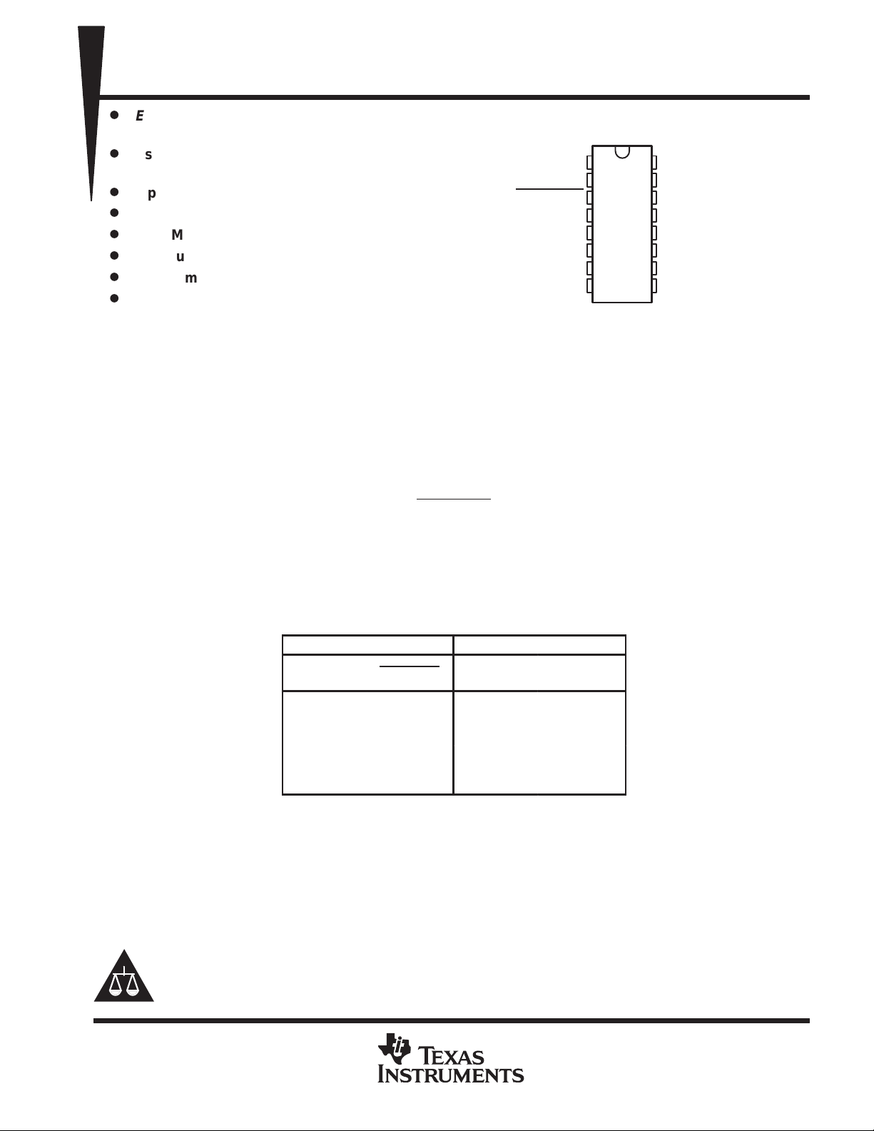
D, DB, OR PW PACKAGE
(TOP VIEW)
I2C SCL
2
I
C SDA
OVERRIDE
MUX IN A
MUX IN B
MUX IN C
MUX IN D
GND
1
2
3
4
5
6
7
8
V
16
CC
WP
15
NON-MUXED OUT
14
MUX SELECT
13
12
MUX OUT A
11
MUX OUT B
10
MUX OUT C
9
MUX OUT D
Small-Outline (D), Shrink Small-Outline
(DB), and Thin Shrink Small-Outline (PW)
Packages
description
This 4-bit 1-of-2 multiplexer with I2C input interface is designed for 3-V to 3.6-V VCC operation.
The PCA8550 is designed to multiplex four bits of data from parallel inputs or from I
nonvolatile register. An additional bit of register output also is provided, which is latched to prevent changes in
the output value during the write cycle. The factory default for the contents of the register is all low. These stored
values can be read from, or written to, using the I
by the write protect (WP) input. The override (OVERRIDE
This device provides a fast-mode (400 kbit/s) or standard-mode (100 kbit/s) I
2
C bus. The ability to control writing to the register is provided
) input forces all the register outputs to a low.
2
and output. The implementation is as a slave. The device address is specified in the I
Both of the I
2
C Schmitt-trigger inputs (SCL and SDA) provide integrated pullup resistors and are 5-V tolerant.
2
C input data stored in a
C serial interface for data input
2
C interface definition table.
The PCA8550 is characterized for operation from 0°C to 70°C.
FUNCTION TABLE
INPUTS
MUX SELECT OVERRIDE MUX OUT
L L L L
L H
H X MUX IN
†
The latched NON-MUXED OUT state is the value present on the
NON-MUXED OUT output at the time the MUX SELECT input
transitions from the low to the high state.
Please be aware that an important notice concerning availability, standard warranty, and use in critical applications of
Texas Instruments semiconductor products and disclaimers thereto appears at the end of this data sheet.
Nonvolatile
register
OUTPUTS
NON-MUXED
Nonvolatile
NON-MUXED
OUT
register
Latched
†
OUT
EPIC is a trademark of Texas Instruments Incorporated.
PRODUCTION DATA information is current as of publication date.
Products conform to specifications per the terms of Texas Instruments
standard warranty. Production processing does not necessarily include
testing of all parameters.
POST OFFICE BOX 655303 • DALLAS, TEXAS 75265
Copyright 1999, Texas Instruments Incorporated
1
PCA8550
NONVOLATILE 5-BIT REGISTER
WITH I
SCPS050A – MARCH 1999 – REVISED APRIL 1999
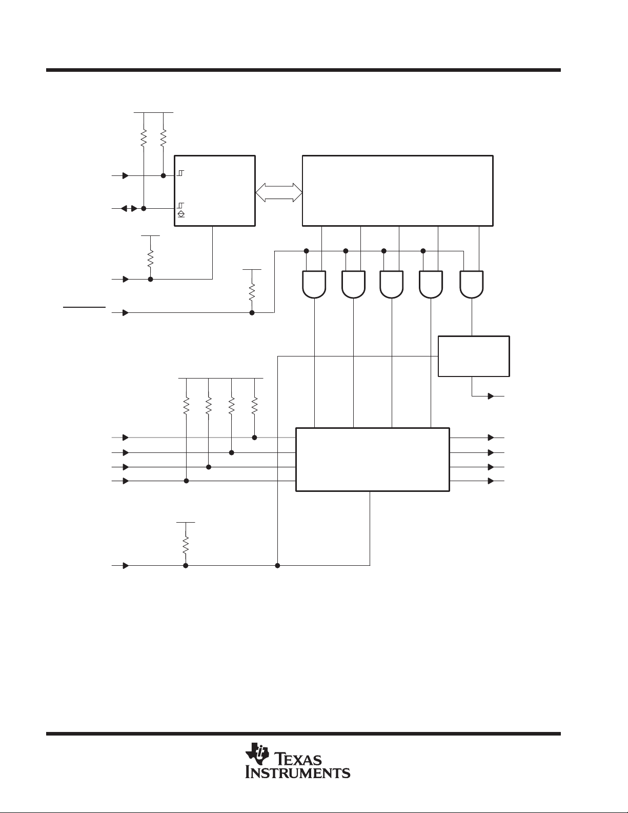
logic diagram (positive logic)
2
C INTERFACE
V
CC
SCL
SDA
WP
OVERRIDE
MUX IN A
MUX IN B
MUX IN C
MUX IN D
1
15
I2C
Interface
Logic
2
V
CC
3
4
5
6
7
Address:
1001110
V
CC
V
CC
5-Bit Nonvolatile Register
4-Bit 1-of-2 Multiplexer
1-Bit
Transparent
Latch
14
NON-MUXED
OUT
12
MUX OUT A
11
MUX OUT B
10
MUX OUT C
9
MUX OUT D
MUX SELECT
2
13
V
CC
POST OFFICE BOX 655303 • DALLAS, TEXAS 75265
BYTE
NONVOLATILE 5-BIT REGISTER
SCPS050A – MARCH 1999 – REVISED APRIL 1999
WITH I
I2C interface
2
I
C communication with this device is initiated by a master sending a start condition, a high-to-low transition on
the serial data (SDA) input/output while the serial clock (SCL) input is high. After the start condition, the device
address byte is sent, MSB first, including the data-direction bit (R/W
general call address. After receiving the valid address byte, this device responds with an acknowledge, a low
on the SDA input/output during the high of the acknowledge-related clock pulse.
). This device does not respond to the
2
C INTERFACE
PCA8550
The data byte follows the address acknowledge. If the R/W
read from the nonvolatile register. If the R/W
bit is low, the data are from the master , to be written into the register.
bit is high, the data from this device are the values
A valid data byte is one in which the three high-order bits are low. The first valid data byte that is received is
written into the register, following the stop condition. If an invalid data byte is received, it is acknowledged, but
is not written into the register. The data byte is followed by an acknowledge sent from this device. If other data
bytes are sent from the master following the acknowledge, they are ignored by this device.
A stop condition, a low-to-high transition on the SDA input/output while the SCL input is high, is sent by the
master. If the WP input is low during the falling edge of the first valid data byte acknowledge on the SCL input
and the R/W
bit is low, the stop condition causes the I2C interface logic to write the data byte value into the
nonvolatile register. Data are written only if complete bytes are received and acknowledged. Writing to the
register takes time (t
2
the I
C interface logic does not write to the register.
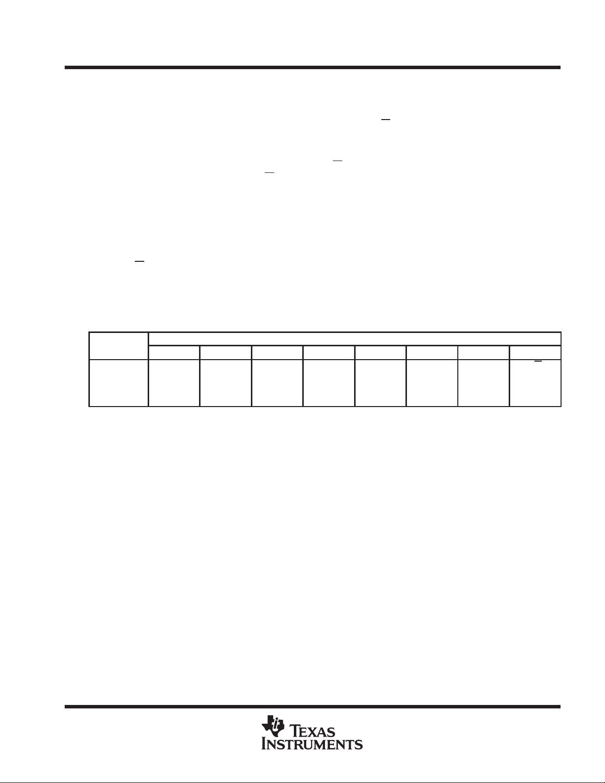
Address H L L H H H L R/W
Data L L L
), during which the device does not respond to its slave address. If the WP input is high,
wr
I2C INTERFACE DEFINITION TABLE
BIT
7 (MSB) 6 5 4 3 2 1
NON-
MUXED
OUT
MUX OUTDMUX OUTCMUX OUTBMUX OUT
0 (LSB)
A
absolute maximum ratings over operating free-air temperature range (unless otherwise noted)
Supply voltage range, V
Input voltage range, V
Output voltage range, V
Output voltage range, V
Output voltage range, V
Input clamp current, I
Output clamp current, I
Input/output clamp current, I
Continuous output current, I
Continuous current through V
Package thermal impedance, θ
Storage temperature range, T
†
Stresses beyond those listed under “absolute maximum ratings” may cause permanent damage to the device. These are stress ratings only, and
functional operation of the device at these or any other conditions beyond those indicated under “recommended operating conditions” is not
implied. Exposure to absolute-maximum-rated conditions for extended periods may affect device reliability.
NOTES: 1. The input negative-voltage and output voltage ratings may be exceeded if the input and output current ratings are observed.
2. The value of VCC is provided in the recommended operating conditions table.
3. The package thermal impedance is calculated in accordance with JESD 51.
–0.5 V to 6.5 V. . . . . . . . . . . . . . . . . . . . . . . . . . . . . . . . . . . . . . . . . . . . . . . . . . . . . . . . .
CC
(see Note 1) –0.5 V to 6.5 V. . . . . . . . . . . . . . . . . . . . . . . . . . . . . . . . . . . . . . . . . . . . . . . . .
I
(SDA) (see Note 1) –0.5 V to 6.5 V. . . . . . . . . . . . . . . . . . . . . . . . . . . . . . . . . . . . . . . .
O
(MUX OUT outputs) (see Note 1) –0.5 V to 2.9 V. . . . . . . . . . . . . . . . . . . . . . . . . . . .
O
(NON-MUXED OUT output) (see Notes 1 and 2) –0.5 V to VCC + 0.5 V. . . . . . . . .
O
(VI < 0 ) –50 mA. . . . . . . . . . . . . . . . . . . . . . . . . . . . . . . . . . . . . . . . . . . . . . . . . . . . . . . . . .
IK
(VO < 0 or VO > VCC) (see Note 2) –50 mA, +10 mA. . . . . . . . . . . . . . . . . . . . . . . .
OK
(VO < 0) –50 mA. . . . . . . . . . . . . . . . . . . . . . . . . . . . . . . . . . . . . . . . . . . . . . . . . . .
OK
(VO = 0 to VCC) (see Note 2) ±15 mA. . . . . . . . . . . . . . . . . . . . . . . . . . . . . . . . . .
O
or GND ±30 mA. . . . . . . . . . . . . . . . . . . . . . . . . . . . . . . . . . . . . . . . . . . . . . . . . . .
CC
(see Note 3): D package 113°C/W. . . . . . . . . . . . . . . . . . . . . . . . . . . . . . . . . .
JA
DB package 131°C/W. . . . . . . . . . . . . . . . . . . . . . . . . . . . . . . .
PW package 149°C/W. . . . . . . . . . . . . . . . . . . . . . . . . . . . . . . .
–65°C to 85°C. . . . . . . . . . . . . . . . . . . . . . . . . . . . . . . . . . . . . . . . . . . . . . . . . . . .
stg
†
POST OFFICE BOX 655303 • DALLAS, TEXAS 75265
3

PCA8550
MUX OUT
V
V
NON-MUXED OUT
MUX OUT
VOLNON-MUXED OUT
V
SDA
A
A
I
NONVOLATILE 5-BIT REGISTER
WITH I
SCPS050A – MARCH 1999 – REVISED APRIL 1999
recommended operating conditions
electrical characteristics over recommended operating free-air temperature range,
V
†
2
C INTERFACE
V
V
V
I
OH
I
OL
∆t/∆v Input transition rise or fall rate
T
CC
V
V
I
IH
I
IL
CC
C
V
Supply voltage 3 3.6 V
CC
High-level input voltage
IH
Low-level input voltage
IL
High-level output current
Low-level output current
Operating free-air temperature 0 70 °C
A
= 3.3 V ± 0.3 V (unless otherwise noted)
PARAMETER TEST CONDITIONS MIN MAX UNIT
IK
hys
OH
i
hys
Input diode clamp voltage II = –18 mA –1.5 V
†
SCL, SDA 0.19 V
IOH = –100 µA 2 2.625
IOH = –1 mA 1.7 2.625
IOH = –100 µA 2.4 3.6
IOH = –2 mA 2 3.6
IOL = 100 µA –0.3 0.4
IOL = 2 mA –0.3 0.7
IOL = 100 µA –0.5 0.4
IOL = 2 mA –0.5 0.7
IOL = 3 mA 0.4
IOL = 6 mA 0.6
SCL, SDA –1.5 –12
OVERRIDE, MUX SELECT, WP
MUX IN –0.166 –0.75 mA
SCL, SDA –7 –32
OVERRIDE, MUX SELECT, WP
MUX IN –0.72 –2 mA
During read or write cycle VI = 0 to VCC, IO = 0, VCC = 3.3 V 10 mA
Not during read or write cycle VI = VCC, IO = 0 500 µA
is the hysteresis of Schmitt-trigger inputs.
VIH = 2.4 V
VIL = 0.4 V
VI = VCC or GND 10 pF
MIN MAX UNIT
SCL, SDA 2.7 4
OVERRIDE
MUX SELECT, WP
SCL, SDA –0.5 0.9
OVERRIDE
MUX SELECT, WP
MUX OUT,
NON-MUXED OUT
SDA 6
MUX OUT,
NON-MUXED OUT
OVERRIDE, MUX IN,
MUX SELECT, WP
, MUX IN,
, MUX IN,
–0.5 0.8
–20 –100
–86 –267
2 4
–2 mA
10 ns/V
V
V
mA
2
µ
µ
4
POST OFFICE BOX 655303 • DALLAS, TEXAS 75265
UNIT
(INPUT)
(OUTPUT)
PCA8550
NONVOLATILE 5-BIT REGISTER
SCPS050A – MARCH 1999 – REVISED APRIL 1999
WITH I
nonvolatile storage specifications
PARAMETER SPECIFICATIONS
Write time (twr) 10 ms, typical
Memory-cell data retention 10 years, minimum
Maximum number of memory-cell write cycles 1000 cycles, minimum
I2C interface timing requirements over recommended operating free-air temperature range (unless
otherwise noted) (see Figure 1)
VCC = 3.3 V ± 0.3 V
MIN MAX
f
scl
T
T
T
T
T
T
T
T
T
T
T
T
C
†
Cb = capacitance of one bus line in pF.
I2C clock frequency 10 400 kHz
I2C clock high time 600 ns
sch
I2C clock low time 1.3 µs
scl
I2C spike time 0 50 ns
sp
I2C serial data setup time 100 ns
sds
I2C serial data hold time 0 900 ns
sdh
I2C input rise time 20 300 ns
icr
I2C input fall time 20 300 ns
icf
I2C output fall time (10-pF to 400-pF bus) 20 + 0.1 C
ocf
I2C bus free time between stop and start 1.3 µs
buf
I2C start or repeated start condition setup 600 ns
sts
I2C start or repeated start condition hold 600 ns
sth
I2C stop condition setup 600 ns
sps
†
I2C bus capacitive load 400 pF
b
2
C INTERFACE
†
b
250 ns
switching characteristics over recommended operating free-air temperature range (unless
otherwise noted) (see Figure 2)
VCC = 3.3 V
± 0.3 V
MIN MAX
30 ns
120 ns
UNIT
t
mpd
t
sov
t
ovn
t
ovm
t
su
t
h
t
r
t
f
PARAMETER
Mux input to output
propagation delay
MUX SELECT to output valid
OVERRIDE to NON-MUXED
OUT output delay
OVERRIDE to MUX OUT
output delay
Setup time
Hold time
Output rise time 1 3 ns/V
Output fall time 1 3 ns/V
FROM
MUX IN MUX OUT 20 ns
MUX SELECT
OVERRIDE
OVERRIDE
WP
WP
Falling edge of first valid data byte
acknowledge on the SCL input
Falling edge of first valid data byte
acknowledge on the SCL input
TO
Output valid 22 ns
NON-MUXED OUT 15 ns
MUX OUT 25 ns
POST OFFICE BOX 655303 • DALLAS, TEXAS 75265
5

PCA8550
NONVOLATILE 5-BIT REGISTER
WITH I
SCPS050A – MARCH 1999 – REVISED APRIL 1999
2
C INTERFACE
PARAMETER MEASUREMENT INFORMATION
VO = 3.3 V
RL = 1 kΩ
DUT
CL = 10 pF or
CL = 400 pF
GND
LOAD CIRCUIT
2 Bytes for Complete Device
Programming
WP
SCL
SDA
Stop
Condition
(P)
T
buf
T
icf
T
Start or
Repeat
Start
Condition
Start
Condition
(S)
T
scl
sth
Bit 7
MSB
t
icr
t
icf
T
icr
T
sds
Bit 6
T
sch
VOLTAGE WAVEFORMS
Bit 0
(R/W
T
sp
T
sdh
LSB
Acknowledge
)
1.5 V
Repeat
Start
Condition
(A)
t
su
t
PHL
t
PLH
Stop
Condition
(P)
1.5 V
t
h
T
sts
T
sps
Stop
Condition
2.7 V
0 V
0.7 × V
0.3 × V
0.7 × V
0.3 × V
CC
CC
CC
CC
BYTE DESCRIPTION
1 I2C address
2 Nonvolatile register data
Figure 1. I2C Interface Load Circuit and Voltage Waveforms
6
POST OFFICE BOX 655303 • DALLAS, TEXAS 75265

PCA8550
NONVOLATILE 5-BIT REGISTER
SCPS050A – MARCH 1999 – REVISED APRIL 1999
WITH I
PARAMETER MEASUREMENT INFORMATION
From Output
Under Test
CL = 15 pF
(see Note A)
LOAD CIRCUIT
2
C INTERFACE
Input
t
PLH
Output
(see Note D)
FOR NON-MUXED OUT OUTPUT
NOTES: A. CL includes probe and jig capacitance.
B. All input pulses are supplied by generators having the following characteristics: PRR ≤ 10 MHz, ZO = 50 Ω, tr ≤ 2.5 ns, tf≤ 2.5 ns.
C. The outputs are measured one at a time with one transition per measurement.
D. t
PLH
E. t
PLH
1.5 V 1.5 V
1.5 V 1.5 V
VOLTAGE WAVEFORMS
PROPAGATION DELAY TIMES
and t
and t
are the same as t
PHL
are the same as t
PHL
sov
mpd
Figure 2. Load Circuit and Voltage Waveforms
t
PHL
and t
, t
sov
2.7 V
0 V
V
V
ovn
, and t
OH
OL
.
ovm
.
Input
Output
(see Note E)
1.5 V 1.5 V
t
PLH
1.25 V 1.25 V
VOLTAGE WAVEFORMS
PROPAGATION DELAY TIMES
FOR MUXED OUT OUTPUTS
t
PHL
2.7 V
0 V
V
OH
V
OL
POST OFFICE BOX 655303 • DALLAS, TEXAS 75265
7

IMPORTANT NOTICE
T exas Instruments and its subsidiaries (TI) reserve the right to make changes to their products or to discontinue
any product or service without notice, and advise customers to obtain the latest version of relevant information
to verify, before placing orders, that information being relied on is current and complete. All products are sold
subject to the terms and conditions of sale supplied at the time of order acknowledgement, including those
pertaining to warranty, patent infringement, and limitation of liability.
TI warrants performance of its semiconductor products to the specifications applicable at the time of sale in
accordance with TI’s standard warranty. Testing and other quality control techniques are utilized to the extent
TI deems necessary to support this warranty . Specific testing of all parameters of each device is not necessarily
performed, except those mandated by government requirements.
CERT AIN APPLICATIONS USING SEMICONDUCTOR PRODUCTS MAY INVOLVE POTENTIAL RISKS OF
DEATH, PERSONAL INJURY, OR SEVERE PROPERTY OR ENVIRONMENTAL DAMAGE (“CRITICAL
APPLICATIONS”). TI SEMICONDUCTOR PRODUCTS ARE NOT DESIGNED, AUTHORIZED, OR
WARRANTED TO BE SUITABLE FOR USE IN LIFE-SUPPORT DEVICES OR SYSTEMS OR OTHER
CRITICAL APPLICA TIONS. INCLUSION OF TI PRODUCTS IN SUCH APPLICATIONS IS UNDERST OOD TO
BE FULLY AT THE CUSTOMER’S RISK.
In order to minimize risks associated with the customer’s applications, adequate design and operating
safeguards must be provided by the customer to minimize inherent or procedural hazards.
TI assumes no liability for applications assistance or customer product design. TI does not warrant or represent
that any license, either express or implied, is granted under any patent right, copyright, mask work right, or other
intellectual property right of TI covering or relating to any combination, machine, or process in which such
semiconductor products or services might be or are used. TI’s publication of information regarding any third
party’s products or services does not constitute TI’s approval, warranty or endorsement thereof.
Copyright 1999, Texas Instruments Incorporated
 Loading...