

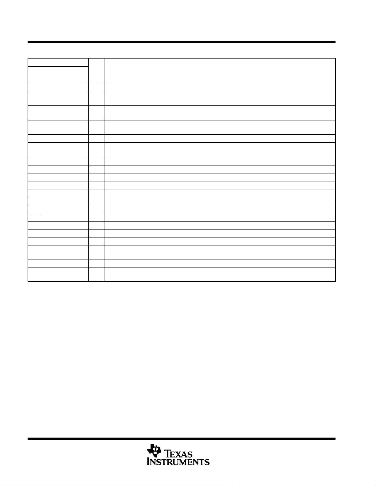
MSP430x43x1, MSP430x43x, MSP430x44x
MIXED SIGNAL MICROCONTROLLER
SLAS344F − JANUARY 2002 − REVISED MAY 2007
D Low Supply-Voltage Range, 1.8 V to 3.6 V
D Ultralow-Power Consumption:
− Active Mode: 280 μA at 1 MHz, 2.2 V
− Standby Mode: 1.1 μA
− Off Mode (RAM Retention): 0.1 μA
D Five Power Saving Modes
D Wake-Up From Standby Mode in Less
Than 6 μs
D 16-Bit RISC Architecture,
125-ns Instruction Cycle Time
D 12-Bit A/D Converter With Internal
Reference, Sample-and-Hold and
Autoscan Feature
D 16-Bit Timer_B With Three
†
or Seven
‡
Capture/Compare-With-Shadow Registers
D 16-Bit Timer_A With Three
Capture/Compare Registers
D On-Chip Comparator
D Serial Communication Interface (USART),
Select Asynchronous UART or
Synchronous SPI by Software:
− Two USARTs (USART0, USART1) —
MSP430x44x Devices
− One USART (USART0) —
MSP430x43x(1) Devices
D Brownout Detector
D Supply Voltage Supervisor/Monitor With
Programmable Level Detection
D Serial Onboard Programming,
No External Programming Voltage Needed
Programmable Code Protection by Security
Fuse
D Integrated LCD Driver for up to
160 Segments
D Bootstrap Loader
D Family Members Include:
− MSP430F435, MSP430F4351
16KB+256B Flash Memory,
512B RAM
− MSP430F436, MSP430F4361
24KB+256B Flash Memory,
1KB RAM
− MSP430F437, MSP430F4371
32KB+256B Flash Memory,
1KB RAM
− MSP430F447:
32KB+256B Flash Memory,
1KB RAM
− MSP430F448:
48KB+256B Flash Memory,
2KB RAM
− MSP430F449:
60KB+256B Flash Memory,
2KB RAM
§
:
§
:
§
:
D For Complete Module Descriptions, See
The MSP430x4xx Family User’s Guide,
Literature Number SLAU056
†
’F435, ’F436, and ’F437 devices
‡
’F447, ’F448, and ’F449 devices
§
The MSP430F43x1 devices are identical to the MSP430F43x
devices with the exception that the ADC12 module is not
implemented.
description
The Texas Instruments MSP430 family of ultralow power microcontrollers consists of several devices featuring
different sets of peripherals targeted for various applications. The architecture, combined with five low-power
modes, is optimized to achieve extended battery life in portable measurement applications. The device features
a powerful 16-bit RISC CPU, 16-bit registers, and constant generators that contribute to maximum code
efficiency. The digitally controlled oscillator (DCO) allows wake-up from low-power modes to active mode in less
than 6 μs.
This integrated circuit can be damaged by ESD. Texas Instruments recommends that all integrated circuits be handled with
appropriate precautions. Failure to observe proper handling and installation procedures can cause damage. ESD damage can range
from subtle performance degradation to complete device failure. Precision integrated circuits may be more susceptible to damage
because very small parametric changes could cause the device not to meet its published specifications. These devices have limited
built-in ESD protection.
Please be aware that an important notice concerning availability, standard warranty, and use in critical applications of
Texas Instruments semiconductor products and disclaimers thereto appears at the end of this data sheet.
PRODUCTION DATA information is current as of publication date.
Products conform to specifications per the terms of Texas Instruments
standard warranty. Production processing does not necessarily include
testing of all parameters.
POST OFFICE BOX 655303 • DALLAS, TEXAS 75265
Copyright © 2002−2007, Texas Instruments Incorporated
1
MSP430x43x1, MSP430x43x, MSP430x44x
MIXED SIGNAL MICROCONTROLLER
SLAS344F − JANUARY 2002 − REVISED MAY 2007
description (continued)
The MSP430x43x(1) and the MSP430x44x series are microcontroller configurations with two built-in 16-bit
timers, a fast 12-bit A/D converter (not implemented on the MSP430F43x1 devices), one or two universal serial
synchronous/asynchronous communication interfaces (USART), 48 I/O pins, and a liquid crystal driver (LCD)
with up to 160 segments.
Typical applications include sensor systems that capture analog signals, convert them to digital values, and
process and transmit the data to a host system, or process this data and display it on a LCD panel. The timers
make the configurations ideal for industrial control applications such as ripple counters, digital motor control,
EE-meters, hand-held meters, etc. The hardware multiplier enhances the performance and offers a broad code
and hardware-compatible family solution.
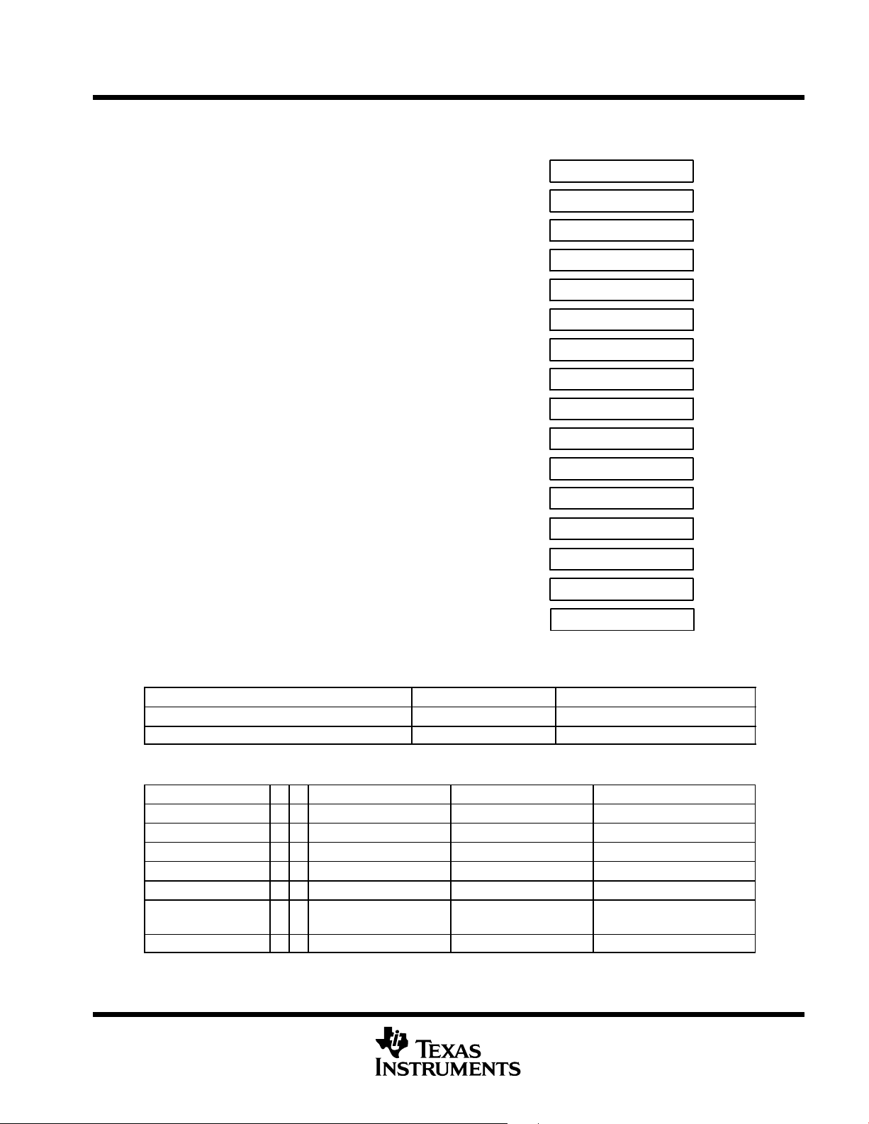
AVAILABLE OPTIONS
PACKAGED DEVICES
T
A
PLASTIC 80-PIN QFP
(PN)
MSP430F435IPN
MSP430F436IPN
MSP430F437IPN
PLASTIC 100-PIN QFP
(PZ)
MSP430F435IPZ
MSP430F436IPZ
MSP430F437IPZ
−40°C to 85°C
MSP430F4351IPN
MSP430F4361IPN
MSP430F4371IPN
MSP430F4351IPZ
MSP430F4361IPZ
MSP430F4371IPZ
MSP430F447IPZ
MSP430F448IPZ
MSP430F449IPZ
2
POST OFFICE BOX 655303 • DALLAS, TEXAS 75265
MSP430x43x1, MSP430x43x, MSP430x44x
MIXED SIGNAL MICROCONTROLLER
SLAS344F − JANUARY 2002 − REVISED MAY 2007
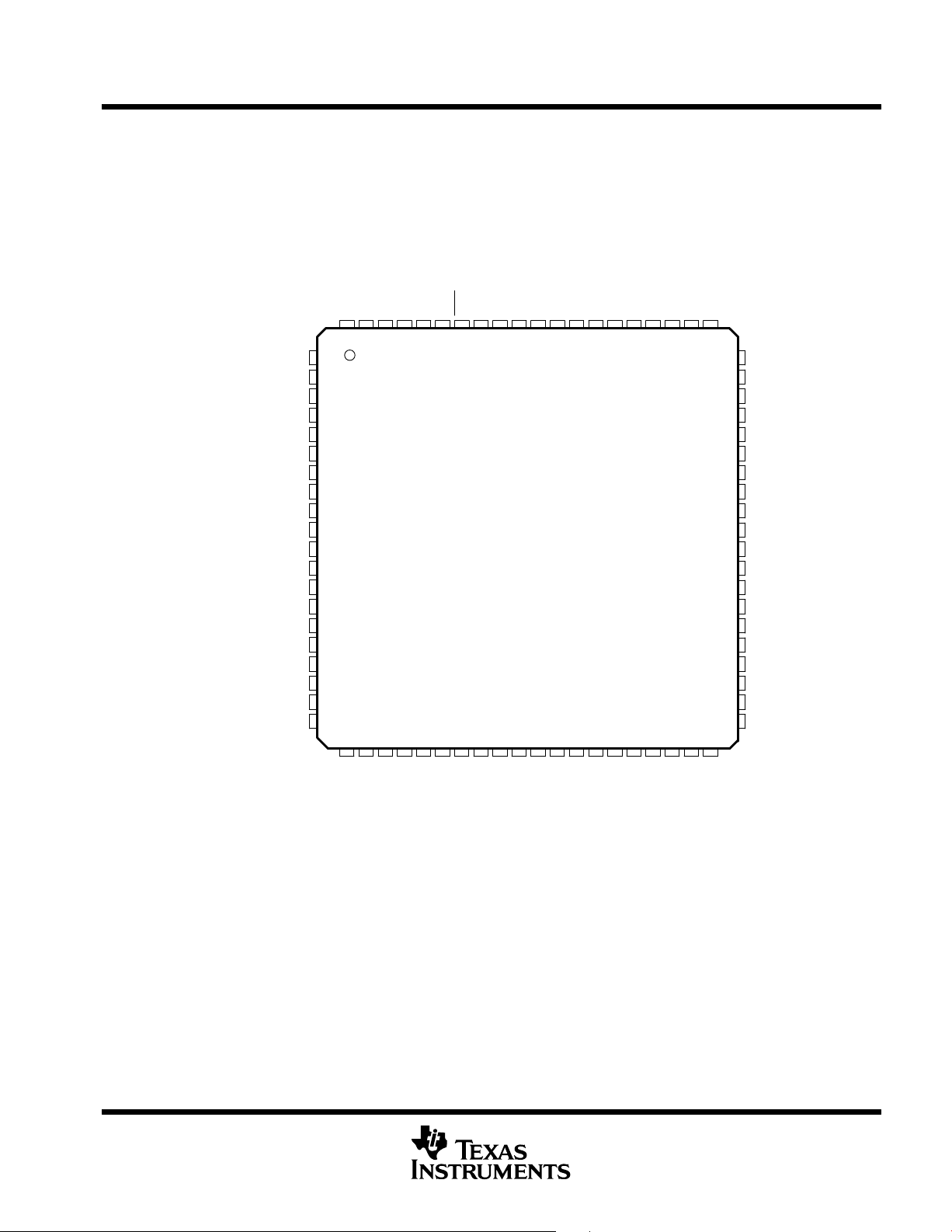
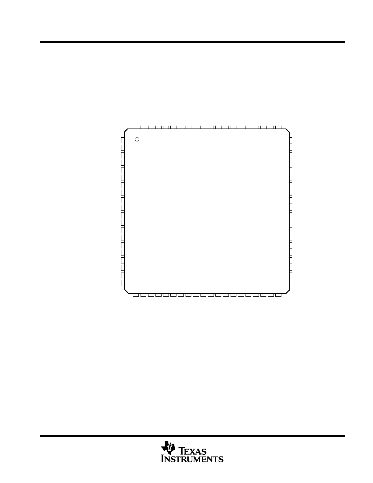
pin designation, MSP430x4351IPN, MSP430x4361IPN, MSP430x4371IPN
PN PACKAGE
(TOP VIEW)
SS1
CCAVSS
XT2OUT
P1.0/TA0
P1.1/TA0/MCLK
P1.2/TA1
DV
AV
P6.2
P6.1
P6.0
RST/NMI
TCK
TMS
TDI/TCLK
TDO/TDI
XT2IN
P1.3/TBOUTH/SVSOUT
P1.6/CA0
P1.4/TBCLK/SMCLK
P1.5/TACLK/ACLK
DV
CC1
P6.3
P6.4
P6.5
P6.6
P6.7/SVSIN
Reserved
XIN
XOUT
DV
SS
DV
SS
P5.1/S0
P5.0/S1
P4.7/S2
P4.6/S3
P4.5/S4
P4.4/S5
P4.3/S6
P4.2/S7
P4.1/S8
79 78 77 76 7580 74
1
2
3
4
5
6
7
8
9
10
11
12
13
14
15
16
17
18
19
20
22 23
21
S10
P4.0/S9
25 26 27 28
24
S11
S12
MSP430F4351IPN
MSP430F4361IPN
MSP430F4371IPN
S13
S14
S15
72 71 7073
29
30 31 32 33
S16
S17
69 68
S20
P2.7/S18
67 66 65 64
34 35 36 37
S22
S23
S21
63 62 61
38 39 40
P3.7/S24
P3.6/S25
P3.5/S26
60
59
58
57
56
55
54
53
52
51
50
49
48
47
46
45
44
43
42
41
P3.4/S27
P1.7/CA1
P2.0/TA2
P2.1/TB0
P2.2/TB1
P2.3/TB2
P2.4/UTXD0
P2.5/URXD0
DV
SS2
DV
CC2
P5.7/R33
P5.6/R23
P5.5/R13
R03
P5.4/COM3
P5.3/COM2
P5.2/COM1
COM0
P3.0/STE0/S31
P3.1/SIMO0/S30
P3.2/SOMI0/S29
P2.6/CAOUT/S19
POST OFFICE BOX 655303 • DALLAS, TEXAS 75265
P3.3/UCLK0/S28
3
MSP430x43x1, MSP430x43x, MSP430x44x
MIXED SIGNAL MICROCONTROLLER
SLAS344F − JANUARY 2002 − REVISED MAY 2007
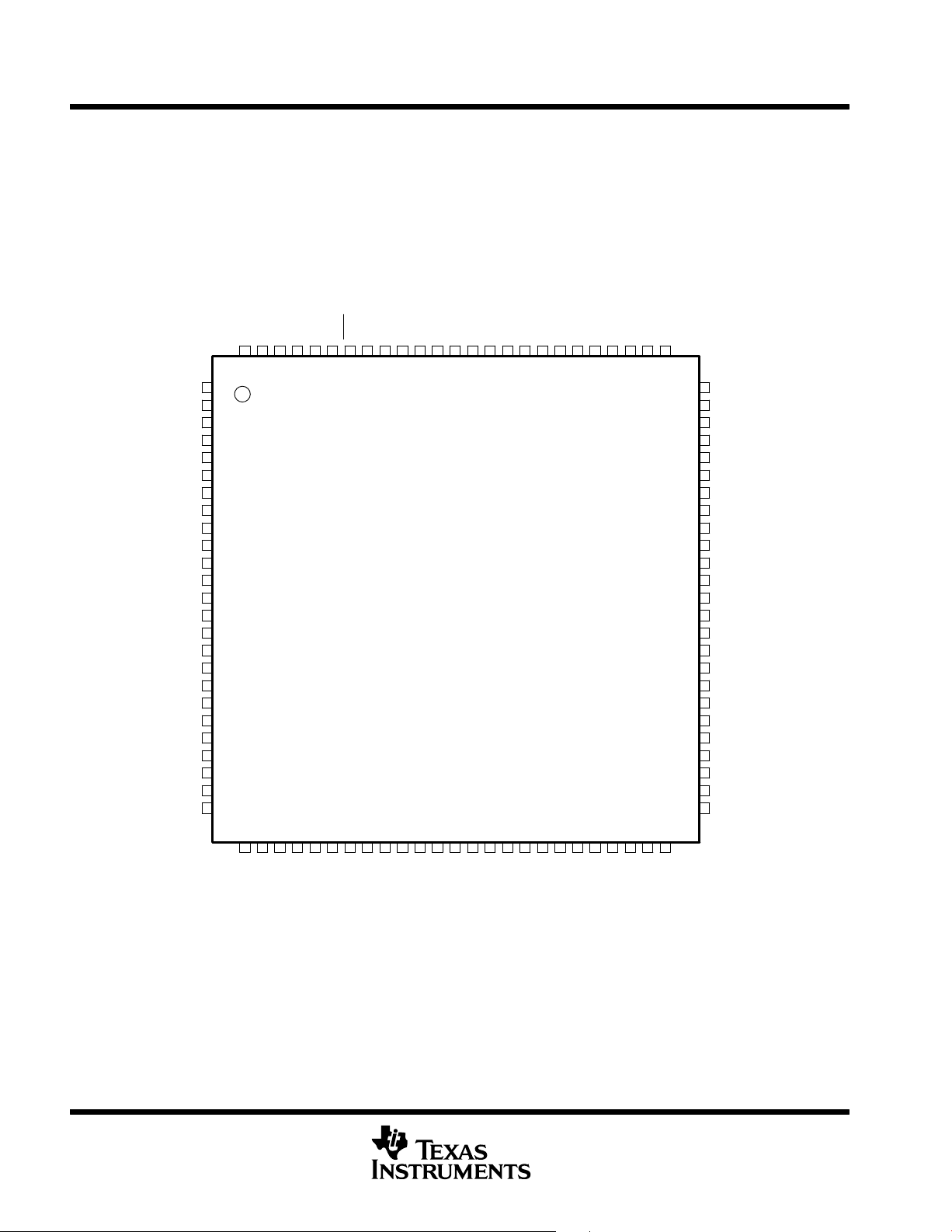
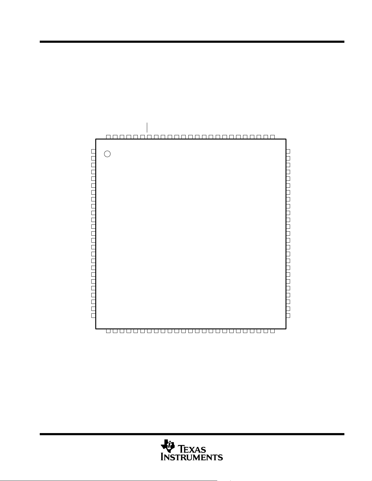
pin designation, MSP430x4351IPZ, MSP430x4361IPZ, MSP430x4371IPZ
PZ PACKAGE
(TOP VIEW)
SS1
CCAVSS
P1.7/CA1
P1.5/TACLK/ACLK
P1.6/CA0
P2.0/TA2
79
80
81
82
47
46
45
44
DV
CC1
P6.3
P6.4
P6.5
P6.6
P6.7/SVSIN
Reserved
XIN
XOUT
DV
SS
DV
SS
P5.1/S0
P5.0/S1
S2
S3
S4
S5
S6
S7
S8
S9
S10
S11
S12
S13
1
2
3
4
5
6
7
8
9
10
11
12
13
14
15
16
17
18
19
20
21
22
23
24
25
100
26
DV
99
27
AV
98
28
P6.2
97
29
P6.1
96
30
P6.0
RST/NMI
94
95
32
31
TDI/TCLK
TCK
93
33
TDO/TDI
TMS
90
91
92
MSP430F4351IPZ
MSP430F4361IPZ
MSP430F4371IPZ
36
35
34
XT2IN
XT2OUT
88
89
38
37
P1.0/TA0
P1.1/TA0/MCLK
86
87
40
39
P1.3/TBOUTH/SVSOUT
P1.4/TBCLK/SMCLK
P1.2/TA1
83
84
85
43
42
41
P2.3/TB2
P2.1/TB0
P2.2/TB1
76
77
78
75
74
73
72
71
70
69
68
67
66
65
64
63
62
61
60
59
58
57
56
55
54
53
52
51
50
49
48
P2.4/UTXD0
P2.5/URXD0
P2.6/CAOUT
P2.7
P3.0/STE0
P3.1/SIMO0
P3.2/SOMI0
P3.3/UCLK0
P3.4
P3.5
P3.6
P3.7
P4.0
P4.1
DV
SS2
DV
CC2
P5.7/R33
P5.6/R23
P5.5/R13
R03
P5.4/COM3
P5.3/COM2
P5.2/COM1
COM0
P4.2/S39
S21
S22
S14
S15
S16
S17
S18
S20
S19
4
POST OFFICE BOX 655303 • DALLAS, TEXAS 75265
S23
S24
S25
S26
S27
S28
S29
S30
S31
S32
S33
P4.7/S34
P4.6/S35
P4.5/S36
P4.4/S37
P4.3/S38
MSP430x43x1, MSP430x43x, MSP430x44x
MIXED SIGNAL MICROCONTROLLER
SLAS344F − JANUARY 2002 − REVISED MAY 2007
pin designation, MSP430x435IPN, MSP430x436IPN, MSP430x437IPN
PN PACKAGE
(TOP VIEW)
SS1
CCAVSS
XT2OUT
P1.0/TA0
P1.1/TA0/MCLK
DV
AV
P6.2/A2
P6.1/A1
P6.0/A0
RST/NMI
TCK
TMS
TDO/TDI
TDI/TCLK
XT2IN
P1.2/TA1
P1.3/TBOUTH/SVSOUT
P1.6/CA0
P1.4/TBCLK/SMCLK
P1.5/TACLK/ACLK
DV
CC1
P6.3/A3
P6.4/A4
P6.5/A5
P6.6/A6
P6.7/A7/SVSIN
VREF+
XIN
XOUT
VeREF+
VREF−/VeREF−
P5.1/S0
P5.0/S1
P4.7/S2
P4.6/S3
P4.5/S4
P4.4/S5
P4.3/S6
P4.2/S7
P4.1/S8
79 78 77 76 7580 74
1
2
3
4
5
6
7
8
9
10
11
12
13
14
15
16
17
18
19
20
22 23
21
S10
P4.0/S9
25 26 27 28
24
S11
S12
S13
72 71 7073
MSP430F435IPN
MSP430F436IPN
MSP430F437IPN
29
S14
S15
S16
69 68
30 31 32 33
S17
67 66 65 64
34 35 36 37
S21
S20
S22
S23
P3.7/S24
63 62 61
38 39 40
P3.6/S25
P3.5/S26
P3.4/S27
P1.7/CA1
60
P2.0/TA2
59
P2.1/TB0
58
P2.2/TB1
57
P2.3/TB2
56
P2.4/UTXD0
55
P2.5/URXD0
54
DV
53
52
51
50
49
48
47
46
45
44
43
42
41
SS2
DV
CC2
P5.7/R33
P5.6/R23
P5.5/R13
R03
P5.4/COM3
P5.3/COM2
P5.2/COM1
COM0
P3.0/STE0/S31
P3.1/SIMO0/S30
P3.2/SOMI0/S29
P2.6/CAOUT/S19
P2.7/ADC12CLK/S18
POST OFFICE BOX 655303 • DALLAS, TEXAS 75265
P3.3/UCLK0/S28
5

MSP430x43x1, MSP430x43x, MSP430x44x
MIXED SIGNAL MICROCONTROLLER
SLAS344F − JANUARY 2002 − REVISED MAY 2007
pin designation, MSP430x435IPZ, MSP430x436IPZ, MSP430x437IPZ
PZ PACKAGE
(TOP VIEW)
SS1
CCAVSS
P1.7/CA1
P1.5/TACLK/ACLK
P1.6/CA0
80
81
82
46
45
44
DV
CC1
P6.3/A3
P6.4/A4
P6.5/A5
P6.6/A6
P6.7/A7/SVSIN
VREF+
XIN
XOUT
VeREF+
VREF−/VeREF−
P5.1/S0
P5.0/S1
S2
S3
S4
S5
S6
S7
S8
S9
S10
S11
S12
S13
1
2
3
4
5
6
7
8
9
10
11
12
13
14
15
16
17
18
19
20
21
22
23
24
25
100
26
DV
99
27
AV
98
28
97
29
P6.1/A1
P6.0/A0
P6.2/A2
95
96
31
30
RST/NMI
TCK
TMS
92
93
94
34
33
32
XT2IN
XT2OUT
89
37
88
38
P1.0/TA0
87
39
TDI/TCLK
TDO/TDI
90
91
MSP430F435IPZ
MSP430F436IPZ
MSP430F437IPZ
36
35
P1.3/TBOUTH/SVSOUT
P1.1/TA0/MCLK
86
40
P1.4/TBCLK/SMCLK
P1.2/TA1
83
84
85
43
42
41
P2.0/TA2
P2.1/TB0
78
79
48
47
P2.3/TB2
P2.2/TB1
76
77
75
74
73
72
71
70
69
68
67
66
65
64
63
62
61
60
59
58
57
56
55
54
53
52
51
50
49
P2.4/UTXD0
P2.5/URXD0
P2.6/CAOUT
P2.7/ADC12CLK
P3.0/STE0
P3.1/SIMO0
P3.2/SOMI0
P3.3/UCLK0
P3.4
P3.5
P3.6
P3.7
P4.0
P4.1
DV
SS2
DV
CC2
P5.7/R33
P5.6/R23
P5.5/R13
R03
P5.4/COM3
P5.3/COM2
P5.2/COM1
COM0
P4.2/S39
S21
S22
S14
S15
S16
S17
S18
S20
S19
6
POST OFFICE BOX 655303 • DALLAS, TEXAS 75265
S23
S24
S25
S26
S27
S28
S29
S30
S31
S32
S33
P4.7/S34
P4.6/S35
P4.5/S36
P4.4/S37
P4.3/S38
MSP430x43x1, MSP430x43x, MSP430x44x
MIXED SIGNAL MICROCONTROLLER
SLAS344F − JANUARY 2002 − REVISED MAY 2007
pin designation, MSP430x447IPZ, MSP430x448IPZ, MSP430x449IPZ
PZ PACKAGE
(TOP VIEW)
SS1
CCAVSS
P1.7/CA1
P1.5/TACLK/ACLK
P1.6/CA0
80
81
82
46
45
44
DV
CC1
P6.3/A3
P6.4/A4
P6.5/A5
P6.6/A6
P6.7/A7/SVSIN
VREF+
XIN
XOUT
VeREF+
VREF−/VeREF−
P5.1/S0
P5.0/S1
S2
S3
S4
S5
S6
S7
S8
S9
S10
S11
S12
S13
1
2
3
4
5
6
7
8
9
10
11
12
13
14
15
16
17
18
19
20
21
22
23
24
25
100
26
DV
99
27
P6.2/A2
AV
97
98
29
28
P6.1/A1
P6.0/A0
RST/NMI
94
95
96
32
31
30
TDI/TCLK
TCK
93
33
TDO/TDI
TMS
90
91
92
MSP430F447IPZ
MSP430F448IPZ
MSP430F449IPZ
36
35
34
XT2IN
XT2OUT
88
89
38
37
P1.0/TA0
P1.1/TA0/MCLK
86
87
40
39
P1.3/TBOUTH/SVSOUT
P1.4/TBCLK/SMCLK
P1.2/TA1
83
84
85
43
42
41
P2.0/TA2
P2.1/TB0
78
79
48
47
P2.3/TB2
P2.2/TB1
76
77
75
74
73
72
71
70
69
68
67
66
65
64
63
62
61
60
59
58
57
56
55
54
53
52
51
50
49
P2.4/UTXD0
P2.5/URXD0
P2.6/CAOUT
P2.7/ADC12CLK
P3.0/STE0
P3.1/SIMO0
P3.2/SOMI0
P3.3/UCLK0
P3.4/TB3
P3.5/TB4
P3.6/TB5
P3.7/TB6
P4.0/UTXD1
P4.1/URXD1
DV
SS2
DV
CC2
P5.7/R33
P5.6/R23
P5.5/R13
R03
P5.4/COM3
P5.3/COM2
P5.2/COM1
COM0
P4.2/STE1/S39
S14
S15
S16
S21
S22
S17
S18
S20
S19
POST OFFICE BOX 655303 • DALLAS, TEXAS 75265
S23
S24
S25
S26
S27
S28
S29
S30
S31
S32
S33
P4.7/S34
P4.6/S35
4.3/SIMO1/S38
P4.4/SOMI1/S37
P4.5/UCLK1/S36
7
MSP430x43x1, MSP430x43x, MSP430x44x
MIXED SIGNAL MICROCONTROLLER
SLAS344F − JANUARY 2002 − REVISED MAY 2007
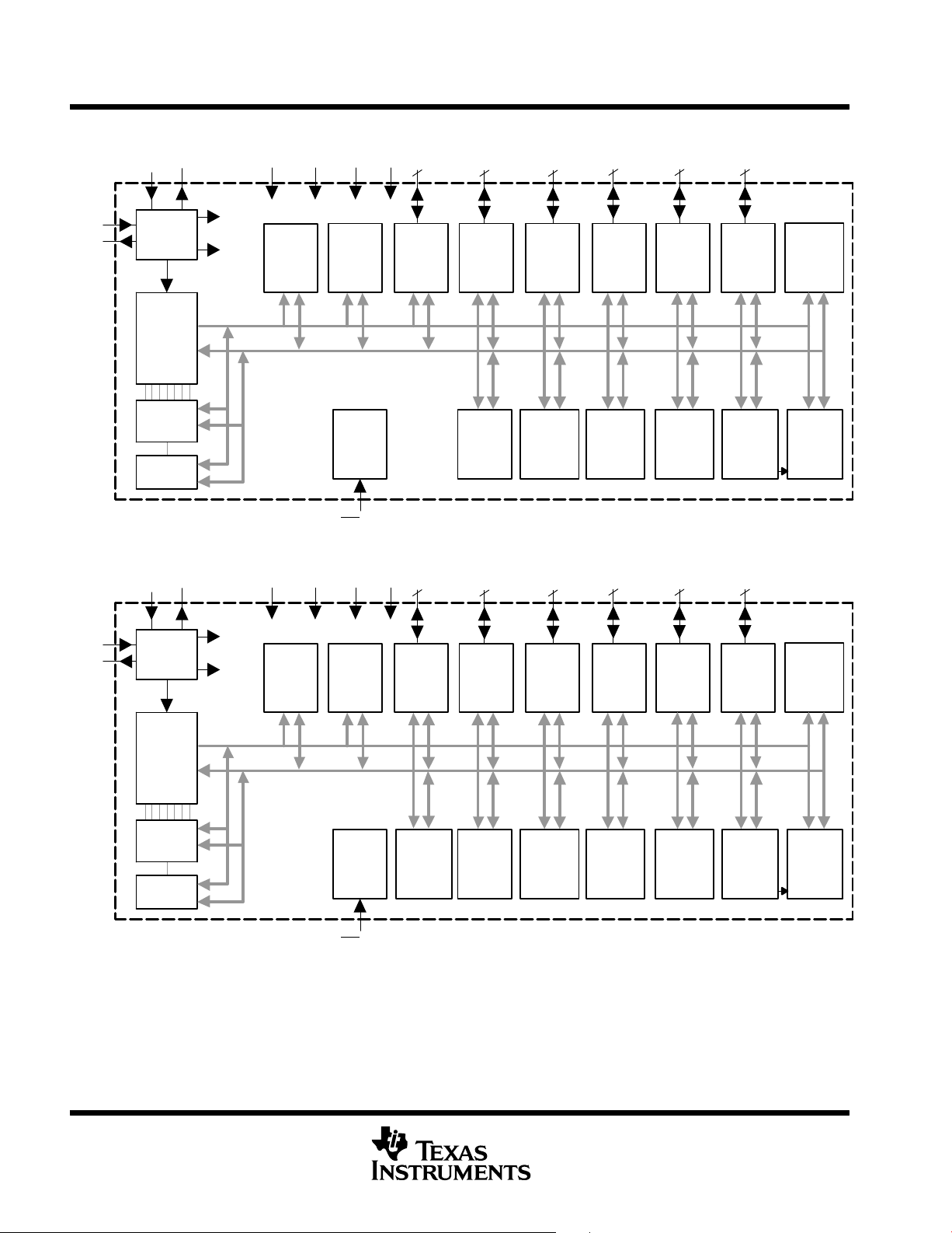
MSP430x43x1 functional block diagram
DV
XIN
XOUT
CC1/2DVSS1/2AVCCAVSS
P1
8
P2
8
P3
P4
8
8
P5
8
P6
8
XT2IN
XT2OUT
Oscillator
FLL+
8 MHz
CPU
incl. 16
Registers
Emulation
Module
JTAG
Interface
MCLK
ACLK
SMCLK
MAB
MDB
Flash
32KB
24KB
16KB
RAM
1KB
512B
POR/
SVS/
Brownout
RST/NMI
MSP430x43x functional block diagram
DV
CC1/2DVSS1/2AVCCAVSS
ACLK
SMCLK
Flash
32KB
24KB
16KB
RAM
1KB
512B
XT2IN
XT2OUT
XIN
Oscillator
FLL+
XOUT
MCLK
Port 1
8 I/O
Interrupt
Capability
P1
8
Port 1
8 I/O
Interrupt
Capability
Port 2
8 I/O
Interrupt
Capability
Watchdog
Timer
WDT
15/16-Bit
P2
8
Port 2
8 I/O
Interrupt
Capability
Port 3
8 I/O
Timer_B3
3 CC Reg
Shadow
Reg
P3
Port 3
8 I/O
8
UART Mode
SPI Mode
Segments
1,2,3,4 MUX
f
LCD
UART Mode
SPI Mode
USART0
LCD
128/160
USART0
Port 4
8 I/O
Timer_A3
3 CC Reg
P4
8
8
Port 4
8 I/O
Port 5
8 I/O
Comparator_
A
P5
8
Port 5
8 I/O
Port 6
6 I/O
Basic
Timer 1
1 Interrupt
Vector
P6
Port 6
6 I/O
8 MHz
CPU
incl. 16
Registers
Emulation
Module
JTAG
Interface
MAB
MDB
POR/
SVS/
Brownout
RST/NMI
ADC12
12-Bit
8 Channels
<10μs Conv.
Watchdog
Timer
WDT
15/16-Bit
Timer_B3
3 CC Reg
Shadow
Reg
Timer_A3
3 CC Reg
Comparator_
A
Basic
Timer 1
1 Interrupt
Vector
Segments
1,2,3,4 MUX
f
LCD
LCD
128/160
8
POST OFFICE BOX 655303 • DALLAS, TEXAS 75265
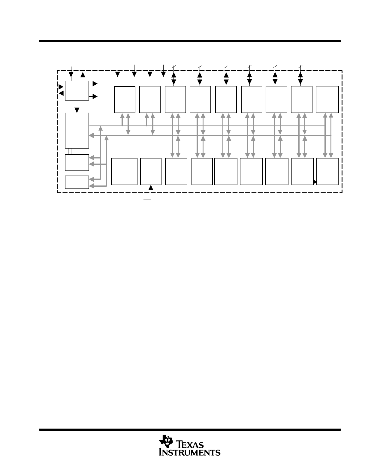
MSP430x44x functional block diagram
DV
XIN
XOUT
CC1/2DVSS1/2AVCCAVSS
MSP430x43x1, MSP430x43x, MSP430x44x
MIXED SIGNAL MICROCONTROLLER
SLAS344F − JANUARY 2002 − REVISED MAY 2007
P1
8
P2
8
P3
P4
8
8
P5
8
P6
8
XT2IN
XT2OUT
Oscillator
FLL+
8 MHz
CPU
incl. 16
Registers
Emulation
Module
JTAG
Interface
MCLK
ACLK
SMCLK
Flash
60KB
48KB
32KB
MAB
MDB
Hardware
Multiplier
MPY, MPYS
MAC,MACS
RAM
2KB
1KB
POR/
SVS/
Brownout
RST/NMI
Port 1
8 I/O
Interrupt
Capability
ADC12
12-Bit
8 Channels
<10μs Conv.
Port 2
8 I/O
Interrupt
Capability
Watchdog
Timer
WDT
15/16-Bit
Port 3
8 I/O
Timer_B7
7 CC Reg
Shadow
Reg
Port 4
8 I/O
Timer_A3
3 CC Reg
Port 5
8 I/O
Comparator_
A
Port 6
6 I/O
Basic
Timer 1
1 Interrupt
Vector
USART0
USART1
UART Mode
SPI Mode
Segments
1,2,3,4 MUX
f
LCD
LCD
160
POST OFFICE BOX 655303 • DALLAS, TEXAS 75265
9
MSP430x43x1, MSP430x43x, MSP430x44x
DESCRIPTION
MIXED SIGNAL MICROCONTROLLER
SLAS344F − JANUARY 2002 − REVISED MAY 2007
MSP430x43x1 Terminal Functions
TERMINAL
PN
NAME NO.
DV
CC1
P6.3 2 I/O P6.3 2 I/O General-purpose digital I/O
P6.4 3 I/O P6.4 3 I/O General-purpose digital I/O
P6.5 4 I/O P6.5 4 I/O General-purpose digital I/O
P6.6 5 I/O P6.6 5 I/O General-purpose digital I/O
P6.7/SVSIN 6 I/O P6.7/SVSIN 6 I/O General-purpose digital I/O / input to brownout, supply voltage
Reserved 7 Reserved 7 Reserved, do not connect externally
XIN 8 I XIN 8 I
XOUT 9 O XOUT 9 O Output terminal of crystal oscillator XT1
DV
SS
DV
SS
P5.1/S0 12 I/O P5.1/S0 12 I/O General-purpose digital I/O / LCD segment output 0
P5.0/S1 13 I/O P5.0/S1 13 I/O General-purpose digital I/O / LCD segment output 1
P4.7/S2 14 I/O S2 14 O General-purpose digital I/O / LCD segment output 2
P4.6/S3 15 I/O S3 15 O General-purpose digital I/O / LCD segment output 3
P4.5/S4 16 I/O S4 16 O General-purpose digital I/O / LCD segment output 4
P4.4/S5 17 I/O S5 17 O General-purpose digital I/O / LCD segment output 5
P4.3/S6 18 I/O S6 18 O General-purpose digital I/O / LCD segment output 6
P4.2/S7 19 I/O S7 19 O General-purpose digital I/O / LCD segment output 7
P4.1/S8 20 I/O S8 20 O General-purpose digital I/O / LCD segment output 8
P4.0/S9 21 I/O S9 21 O General-purpose digital I/O / LCD segment output 9
S10 22 O S10 22 O LCD segment output 10
S11 23 O S11 23 O LCD segment output 11
S12 24 O S12 24 O LCD segment output 12
S13 25 O S13 25 O LCD segment output 13
S14 26 O S14 26 O LCD segment output 14
S15 27 O S15 27 O LCD segment output 15
S16 28 O S16 28 O LCD segment output 16
S17 29 O S17 29 O LCD segment output 17
P2.7/S18 30 I/O S18 30 O General-purpose digital I/O / LCD segment output 18
P2.6/CAOUT/S19 31 I/O S19 31 O
S20 32 O S20 32 O LCD segment output 20
S21 33 O S21 33 O LCD segment output 21
S22 34 O S22 34 O LCD segment output 22
S23 35 O S23 35 O LCD segment output 23
P3.7/S24 36 I/O S24 36 O General-purpose digital I/O / LCD segment output 24
P3.6/S25 37 I/O S25 37 O General-purpose digital I/O / LCD segment output 25
P3.5/S26 38 I/O S26 38 O General-purpose digital I/O / LCD segment output 26
P3.4/S27 39 I/O S27 39 O General-purpose digital I/O / LCD segment output 27
I/O
1 DV
10 I DV
11 I DV
PZ
NAME NO.
CC1
SS
SS
I/O
1 Digital supply voltage, positive terminal.
supervisor
Input port for crystal oscillator XT1. Standard or watch crystals can be
connected.
10 I Connect to DV
11 I Connect to DV
General-purpose digital I/O / Comparator_A output / LCD segment
output 19
SS
SS
DESCRIPTION
10
POST OFFICE BOX 655303 • DALLAS, TEXAS 75265
MSP430x43x1, MSP430x43x, MSP430x44x
DESCRIPTION
MIXED SIGNAL MICROCONTROLLER
SLAS344F − JANUARY 2002 − REVISED MAY 2007
MSP430x43x1 Terminal Functions (Continued)
TERMINAL
PN
NAME NO.
P3.3/UCLK0/S28 40 I/O S28 40 O
P3.2/SOMI0/S29 41 I/O S29 41 O
P3.1/SIMO0/S30 42 I/O S30 42 O
P3.0/STE0/S31 43 I/O S31 43 O
COM0 44 O COM0 52 O COM0−3 are used for LCD backplanes.
P5.2/COM1 45 I/O P5.2/COM1 53 I/O
P5.3/COM2 46 I/O P5.3/COM2 54 I/O
P5.4/COM3 47 I/O P5.4/COM3 55 I/O
R03 48 I R03 56 I Input port of fourth positive (lowest) analog LCD level (V5)
P5.5/R13 49 I/O P5.5/R13 57 I/O
P5.6/R23 50 I/O P5.6/R23 58 I/O
P5.7/R33 51 I/O P5.7/R33 59 I/O
DV
CC2
DV
SS2
P2.5/URXD0 54 I/O P2.5/URXD0 74 I/O General-purpose digital I/O / receive data in—USART0/UART mode
I/O
S32 44 O LCD segment output 32
S33 45 O LCD segment output 33
P4.7/S34 46 I/O General-purpose digital I/O / LCD segment output 34
P4.6/S35 47 I/O General-purpose digital I/O / LCD segment output 35
P4.5/S36 48 I/O General-purpose digital I/O / LCD segment output 36
P4.4/S37 49 I/O General-purpose digital I/O / LCD segment output 37
P4.3/S38 50 I/O General-purpose digital I/O / LCD segment output 38
P4.2/S39 51 I/O General-purpose digital I/O / LCD segment output 39
52 DV
53 DV
P4.1 62 I/O General-purpose digital I/O
P4.0 63 I/O General-purpose digital I/O
P3.7 64 I/O General-purpose digital I/O
P3.6 65 I/O General-purpose digital I/O
P3.5 66 I/O General-purpose digital I/O
P3.4 67 I/O General-purpose digital I/O
P3.3/UCLK0 68 I/O
P3.2/SOMI0 69 I/O General-purpose digital I/O / slave out/master in of USART0/SPI mode
P3.1/SIMO0 70 I/O General-purpose digital I/O / slave in/master out of USART0/SPI mode
P3.0/STE0 71 I/O General-purpose digital I/O / slave transmit enable USART0/SPI mode
P2.7 72 I/O General-purpose digital I/O
P2.6/CAOUT 73 I/O General-purpose digital I/O / Comparator_A output
PZ
NAME NO.
CC2
SS2
I/O
General-purpose digital I/O / ext. clock i/p—USART0/UART or SPI
mode, clock o/p—USART0/SPI mode / LCD segment output 28
General-purpose digital I/O / slave out/master in of USART0/SPI mode
/ LCD segment output 29
General-purpose digital I/O / slave out/master out of USART0/SPI
mode / LCD segment output 30
General-purpose digital I/O / slave transmit enable-USART0/SPI
mode / LCD segment output 31
General-purpose digital I/O / common output, COM0−3 are used for
LCD backplanes.
General-purpose digital I/O / common output, COM0−3 are used for
LCD backplanes.
General-purpose digital I/O / common output, COM0−3 are used for
LCD backplanes.
General-purpose digital I/O / input port of third most positive analog
LCD level (V4 or V3)
General-purpose digital I/O / input port of second most positive analog
LCD level (V2)
General-purpose digital I/O / output port of most positive analog LCD
level (V1)
60 Digital supply voltage, positive terminal.
61 Digital supply voltage, negative terminal.
General-purpose digital I/O / external clock input—USART0/UART or
SPI mode, clock output—USART0/SPI mode
DESCRIPTION
POST OFFICE BOX 655303 • DALLAS, TEXAS 75265
11
MSP430x43x1, MSP430x43x, MSP430x44x
DESCRIPTION
MIXED SIGNAL MICROCONTROLLER
SLAS344F − JANUARY 2002 − REVISED MAY 2007
MSP430x43x1 Terminal Functions (Continued)
TERMINAL
PN
NAME NO.
P2.4/UTXD0 55 I/O P2.4/UTXD0 75 I/O General-purpose digital I/O / transmit data out—USART0/UART mode
P2.3/TB2 56 I/O P2.3/TB2 76 I/O
P2.2/TB1 57 I/O P2.2/TB1 77 I/O
P2.1/TB0 58 I/O P2.1/TB0 78 I/O
P2.0/TA2 59 I/O P2.0/TA2 79 I/O
P1.7/CA1 60 I/O P1.7/CA1 80 I/O General-purpose digital I/O / Comparator_A input
P1.6/CA0 61 I/O P1.6/CA0 81 I/O General-purpose digital I/O / Comparator_A input
P1.5/TACLK/
ACLK
P1.4/TBCLK/
SMCLK
P1.3/TBOUTH/
SVSOUT
P1.2/TA1 65 I/O P1.2/TA1 85 I/O
P1.1/TA0/MCLK 66 I/O P1.1/TA0/MCLK 86 I/O
P1.0/TA0 67 I/O P1.0/TA0 87 I/O
XT2OUT 68 O XT2OUT 88 O Output terminal of crystal oscillator XT2
XT2IN 69 I XT2IN 89 I
TDO/TDI 70 I/O TDO/TDI 90 I/O
TDI/TCLK 71 I TDI/TCLK 91 I
TMS 72 I TMS 92 I
TCK 73 I TCK 93 I Test clock. TCK is the clock input port for device programming and test.
RST/NMI 74 I RST/NMI 94 I
P6.0 75 I/O P6.0 95 I/O General-purpose digital I/O
P6.1 76 I/O P6.1 96 I/O General-purpose digital I/O
P6.2 77 I/O P6.2 97 I/O General-purpose digital I/O
AV
SS
DV
SS1
AV
CC
I/O
62 I/O
63 I/O
64 I/O
78 AV
79 DV
80 AV
P1.5/TACLK/
ACLK
P1.4/TBCLK/
SMCLK
P1.3/TBOUTH/
SVSOUT
SS
CC
PZ
NAME NO.
SS1
I/O
General-purpose digital I/O / Timer_B3 CCR2.
Capture: CCI2A/CCI2B input, compare: Out2 output
General-purpose digital I/O / Timer_B3 CCR1.
Capture: CCI1A/CCI1B input, compare: Out1 output
General-purpose digital I/O / Timer_B3 CCR0.
Capture: CCI0A/CCI0B input, compare: Out0 output
General-purpose digital I/O / Timer_A
Capture: CCI2A input, compare: Out2 output
82 I/O
83 I/O
84 I/O
98
99 Digital supply voltage, negative terminal.
100
General-purpose digital I/O / Timer_A, clock signal TACLK input /
ACLK output (divided by 1, 2, 4, or 8)
General-purpose digital I/O / input clock TBCLK—Timer_B3 / submain
system clock SMCLK output
General-purpose digital I/O / switch all PWM digital output ports to high
impedance—Timer_B3 TB0 to TB2 / SVS: output of SVS comparator
General-purpose digital I/O / Timer_A, Capture: CCI1A input,
compare: Out1 output
General-purpose digital I/O / Timer_A. Capture: CCI0B input / MCLK
output. Note: TA0 is only an input on this pin / BSL receive
General-purpose digital I/O / Timer_A. Capture: CCI0A input,
compare: Out0 output / BSL transmit
Input port for crystal oscillator XT2. Only standard crystals can be
connected.
Test data output port. TDO/TDI data output or programming data input
terminal
Test data input or test clock input. The device protection fuse is
connected to TDI/TCLK.
Test mode select. TMS is used as an input port for device programming
and test.
General-purpose digital I/O / reset input or nonmaskable interrupt input
port
Analog supply voltage, negative terminal. Supplies SVS, brownout,
oscillator, comparator_A, port 1, and LCD resistive divider circuitry.
Analog supply voltage, positive terminal. Supplies SVS, brownout,
oscillator, comparator_A, port 1, and LCD resistive divider circuitry;
must not power up prior to DV
DESCRIPTION
/DV
CC1
CC2
.
12
POST OFFICE BOX 655303 • DALLAS, TEXAS 75265
MSP430x43x1, MSP430x43x, MSP430x44x
DESCRIPTION
MIXED SIGNAL MICROCONTROLLER
SLAS344F − JANUARY 2002 − REVISED MAY 2007
MSP430x43x Terminal Functions
TERMINAL
PN
NAME NO.
DV
CC1
I/O
1 DV
P6.3/A3 2 I/O P6.3/A3 2 I/O General-purpose digital I/O / analog input a3—12-bit ADC
P6.4/A4 3 I/O P6.4/A4 3 I/O General-purpose digital I/O / analog input a4—12-bit ADC
P6.5/A5 4 I/O P6.5/A5 4 I/O General-purpose digital I/O / analog input a5—12-bit ADC
P6.6/A6 5 I/O P6.6/A6 5 I/O General-purpose digital I/O / analog input a6—12-bit ADC
P6.7/A7/SVSIN 6 I/O P6.7/A7/SVSIN 6 I/O General-purpose digital I/O / analog input a7—12-bit ADC, analog /
V
REF+
7 O V
REF+
XIN 8 I XIN 8 I
XOUT 9 O XOUT 9 O Output terminal of crystal oscillator XT1
Ve
V
REF+
REF−
/Ve
REF−
10 I Ve
11 I V
REF+
REF−
P5.1/S0 12 I/O P5.1/S0 12 I/O General-purpose digital I/O / LCD segment output 0
P5.0/S1 13 I/O P5.0/S1 13 I/O General-purpose digital I/O / LCD segment output 1
P4.7/S2 14 I/O S2 14 O General-purpose digital I/O / LCD segment output 2
P4.6/S3 15 I/O S3 15 O General-purpose digital I/O / LCD segment output 3
P4.5/S4 16 I/O S4 16 O General-purpose digital I/O / LCD segment output 4
P4.4/S5 17 I/O S5 17 O General-purpose digital I/O / LCD segment output 5
P4.3/S6 18 I/O S6 18 O General-purpose digital I/O / LCD segment output 6
P4.2/S7 19 I/O S7 19 O General-purpose digital I/O / LCD segment output 7
P4.1/S8 20 I/O S8 20 O General-purpose digital I/O / LCD segment output 8
P4.0/S9 21 I/O S9 21 O General-purpose digital I/O / LCD segment output 9
S10 22 O S10 22 O LCD segment output 10
S11 23 O S11 23 O LCD segment output 11
S12 24 O S12 24 O LCD segment output 12
S13 25 O S13 25 O LCD segment output 13
S14 26 O S14 26 O LCD segment output 14
S15 27 O S15 27 O LCD segment output 15
S16 28 O S16 28 O LCD segment output 16
S17 29 O S17 29 O LCD segment output 17
P2.7/ADC12CLK/
30 I/O S18 30 O General-purpose digital I/O / conversion clock—12-bit ADC / LCD
S18
P2.6/CAOUT/S19 31 I/O S19 31 O
S20 32 O S20 32 O LCD segment output 20
S21 33 O S21 33 O LCD segment output 21
S22 34 O S22 34 O LCD segment output 22
S23 35 O S23 35 O LCD segment output 23
P3.7/S24 36 I/O S24 36 O General-purpose digital I/O / LCD segment output 24
P3.6/S25 37 I/O S25 37 O General-purpose digital I/O / LCD segment output 25
P3.5/S26 38 I/O S26 38 O General-purpose digital I/O / LCD segment output 26
P3.4/S27 39 I/O S27 39 O General-purpose digital I/O / LCD segment output 27
PZ
NAME NO.
CC1
/Ve
REF−
I/O
DESCRIPTION
1 Digital supply voltage, positive terminal.
input to brownout, supply voltage supervisor
7 O Output of positive terminal of the reference voltage in the ADC
Input port for crystal oscillator XT1. Standard or watch crystals can be
connected.
10 I Input for an external reference voltage to the ADC
11 I
Negative terminal for the ADC’s reference voltage for both sources, the
internal reference voltage, or an external applied reference voltage.
segment output 18
General-purpose digital I/O / Comparator_A output / LCD segment
output 19
POST OFFICE BOX 655303 • DALLAS, TEXAS 75265
13
MSP430x43x1, MSP430x43x, MSP430x44x
DESCRIPTION
MIXED SIGNAL MICROCONTROLLER
SLAS344F − JANUARY 2002 − REVISED MAY 2007
MSP430x43x Terminal Functions (Continued)
TERMINAL
PN
NAME NO.
P3.3/UCLK0/S28 40 I/O S28 40 O
P3.2/SOMI0/S29 41 I/O S29 41 O
P3.1/SIMO0/S30 42 I/O S30 42 O
P3.0/STE0/S31 43 I/O S31 43 O
COM0 44 O COM0 52 O COM0−3 are used for LCD backplanes.
P5.2/COM1 45 I/O P5.2/COM1 53 I/O
P5.3/COM2 46 I/O P5.3/COM2 54 I/O
P5.4/COM3 47 I/O P5.4/COM3 55 I/O
R03 48 I R03 56 I Input port of fourth positive (lowest) analog LCD level (V5)
P5.5/R13 49 I/O P5.5/R13 57 I/O
P5.6/R23 50 I/O P5.6/R23 58 I/O
P5.7/R33 51 I/O P5.7/R33 59 I/O
DV
CC2
DV
SS2
P2.5/URXD0 54 I/O P2.5/URXD0 74 I/O General-purpose digital I/O / receive data in—USART0/UART mode
I/O
S32 44 O LCD segment output 32
S33 45 O LCD segment output 33
P4.7/S34 46 I/O General-purpose digital I/O / LCD segment output 34
P4.6/S35 47 I/O General-purpose digital I/O / LCD segment output 35
P4.5/S36 48 I/O General-purpose digital I/O / LCD segment output 36
P4.4/S37 49 I/O General-purpose digital I/O / LCD segment output 37
P4.3/S38 50 I/O General-purpose digital I/O / LCD segment output 38
P4.2/S39 51 I/O General-purpose digital I/O / LCD segment output 39
52 DV
53 DV
P4.1 62 I/O General-purpose digital I/O
P4.0 63 I/O General-purpose digital I/O
P3.7 64 I/O General-purpose digital I/O
P3.6 65 I/O General-purpose digital I/O
P3.5 66 I/O General-purpose digital I/O
P3.4 67 I/O General-purpose digital I/O
P3.3/UCLK0 68 I/O
P3.2/SOMI0 69 I/O General-purpose digital I/O / slave out/master in of USART0/SPI mode
P3.1/SIMO0 70 I/O General-purpose digital I/O / slave in/master out of USART0/SPI mode
P3.0/STE0 71 I/O General-purpose digital I/O / slave transmit enable USART0/SPI mode
P2.7/ADC12CLK 72 I/O General-purpose digital I/O / conversion clock—12-bit ADC
P2.6/CAOUT 73 I/O General-purpose digital I/O / Comparator_A output
PZ
NAME NO.
CC2
SS2
I/O
General-purpose digital I/O / ext. clock i/p—USART0/UART or SPI
mode, clock o/p—USART0/SPI mode / LCD segment output 28
General-purpose digital I/O / slave out/master in of USART0/SPI mode
/ LCD segment output 29
General-purpose digital I/O / slave out/master out of USART0/SPI
mode / LCD segment output 30
General-purpose digital I/O / slave transmit enable-USART0/SPI
mode / LCD segment output 31
General-purpose digital I/O / common output, COM0−3 are used for
LCD backplanes.
General-purpose digital I/O / common output, COM0−3 are used for
LCD backplanes.
General-purpose digital I/O / common output, COM0−3 are used for
LCD backplanes.
General-purpose digital I/O / input port of third most positive analog
LCD level (V4 or V3)
General-purpose digital I/O / input port of second most positive analog
LCD level (V2)
General-purpose digital I/O / output port of most positive analog LCD
level (V1)
60 Digital supply voltage, positive terminal.
61 Digital supply voltage, negative terminal.
General-purpose digital I/O / external clock input—USART0/UART or
SPI mode, clock output—USART0/SPI mode
DESCRIPTION
14
POST OFFICE BOX 655303 • DALLAS, TEXAS 75265
MSP430x43x1, MSP430x43x, MSP430x44x
DESCRIPTION
MIXED SIGNAL MICROCONTROLLER
SLAS344F − JANUARY 2002 − REVISED MAY 2007
MSP430x43x Terminal Functions (Continued)
TERMINAL
PN
NAME NO.
P2.4/UTXD0 55 I/O P2.4/UTXD0 75 I/O General-purpose digital I/O / transmit data out—USART0/UART mode
P2.3/TB2 56 I/O P2.3/TB2 76 I/O
P2.2/TB1 57 I/O P2.2/TB1 77 I/O
P2.1/TB0 58 I/O P2.1/TB0 78 I/O
P2.0/TA2 59 I/O P2.0/TA2 79 I/O
P1.7/CA1 60 I/O P1.7/CA1 80 I/O General-purpose digital I/O / Comparator_A input
P1.6/CA0 61 I/O P1.6/CA0 81 I/O General-purpose digital I/O / Comparator_A input
P1.5/TACLK/
ACLK
P1.4/TBCLK/
SMCLK
P1.3/TBOUTH/
SVSOUT
P1.2/TA1 65 I/O P1.2/TA1 85 I/O
P1.1/TA0/MCLK 66 I/O P1.1/TA0/MCLK 86 I/O
P1.0/TA0 67 I/O P1.0/TA0 87 I/O
XT2OUT 68 O XT2OUT 88 O Output terminal of crystal oscillator XT2
XT2IN 69 I XT2IN 89 I
TDO/TDI 70 I/O TDO/TDI 90 I/O
TDI/TCLK 71 I TDI/TCLK 91 I
TMS 72 I TMS 92 I
TCK 73 I TCK 93 I Test clock. TCK is the clock input port for device programming and test.
RST/NMI 74 I RST/NMI 94 I
P6.0/A0 75 I/O P6.0/A0 95 I/O General-purpose digital I/O / analog input a0 − 12-bit ADC
P6.1/A1 76 I/O P6.1/A1 96 I/O General-purpose digital I/O / analog input a1 − 12-bit ADC
P6.2/A2 77 I/O P6.2/A2 97 I/O General-purpose digital I/O / analog input a2 − 12-bit ADC
AV
SS
DV
SS1
AV
CC
I/O
62 I/O
63 I/O
64 I/O
78 AV
79 DV
80 AV
P1.5/TACLK/
ACLK
P1.4/TBCLK/
SMCLK
P1.3/TBOUTH/
SVSOUT
SS
CC
PZ
NAME NO.
SS1
I/O
General-purpose digital I/O / Timer_B3 CCR2.
Capture: CCI2A/CCI2B input, compare: Out2 output
General-purpose digital I/O / Timer_B3 CCR1.
Capture: CCI1A/CCI1B input, compare: Out1 output
General-purpose digital I/O / Timer_B3 CCR0.
Capture: CCI0A/CCI0B input, compare: Out0 output
General-purpose digital I/O / Timer_A
Capture: CCI2A input, compare: Out2 output
82 I/O
83 I/O
84 I/O
98
99 Digital supply voltage, negative terminal.
100
General-purpose digital I/O / Timer_A, clock signal TACLK input /
ACLK output (divided by 1, 2, 4, or 8)
General-purpose digital I/O / input clock TBCLK—Timer_B3 / submain
system clock SMCLK output
General-purpose digital I/O / switch all PWM digital output ports to high
impedance—Timer_B3 TB0 to TB2 / SVS: output of SVS comparator
General-purpose digital I/O / Timer_A, Capture: CCI1A input,
compare: Out1 output
General-purpose digital I/O / Timer_A. Capture: CCI0B input / MCLK
output. Note: TA0 is only an input on this pin / BSL receive
General-purpose digital I/O / Timer_A. Capture: CCI0A input,
compare: Out0 output / BSL transmit
Input port for crystal oscillator XT2. Only standard crystals can be
connected.
Test data output port. TDO/TDI data output or programming data input
terminal
Test data input or test clock input. The device protection fuse is
connected to TDI/TCLK.
Test mode select. TMS is used as an input port for device programming
and test.
General-purpose digital I/O / reset input or nonmaskable interrupt input
port
Analog supply voltage, negative terminal. Supplies SVS, brownout,
oscillator, comparator_A, ADC12, port 1, and LCD resistive divider
circuitry.
Analog supply voltage, positive terminal. Supplies SVS, brownout,
oscillator, comparator_A, ADC12, port 1, and LCD resistive divider
circuitry; must not power up prior to DV
DESCRIPTION
CC1
/DV
CC2
.
POST OFFICE BOX 655303 • DALLAS, TEXAS 75265
15
MSP430x43x1, MSP430x43x, MSP430x44x
MIXED SIGNAL MICROCONTROLLER
SLAS344F − JANUARY 2002 − REVISED MAY 2007
MSP430x44x Terminal Functions
TERMINAL
NAME NO.
DV
CC1
P6.3/A3 2 I/O General-purpose digital I/O / analog input a3—12-bit ADC
P6.4/A4 3 I/O General-purpose digital I/O / analog input a4—12-bit ADC
P6.5/A5 4 I/O General-purpose digital I/O / analog input a5—12-bit ADC
P6.6/A6 5 I/O General-purpose digital I/O / analog input a6—12-bit ADC
P6.7/A7/SVSIN 6 I/O
V
REF+
XIN 8 I Input port for crystal oscillator XT1. Standard or watch crystals can be connected.
XOUT 9 O Output terminal of crystal oscillator XT1
Ve
REF+
V
/Ve
REF−
REF−
P5.1/S0 12 I/O General-purpose digital I/O / LCD segment output 0
P5.0/S1 13 I/O General-purpose digital I/O / LCD segment output 1
S2 14 O LCD segment output 2
S3 15 O LCD segment output 3
S4 16 O LCD segment output 4
S5 17 O LCD segment output 5
S6 18 O LCD segment output 6
S7 19 O LCD segment output 7
S8 20 O LCD segment output 8
S9 21 O LCD segment output 9
S10 22 O LCD segment output 10
S11 23 O LCD segment output 11
S12 24 O LCD segment output 12
S13 25 O LCD segment output 13
S14 26 O LCD segment output 14
S15 27 O LCD segment output 15
S16 28 O LCD segment output 16
S17 29 O LCD segment output 17
S18 30 O LCD segment output 18
S19 31 O LCD segment output 19
S20 32 O LCD segment output 20
S21 33 O LCD segment output 21
S22 34 O LCD segment output 22
S23 35 O LCD segment output 23
S24 36 O LCD segment output 24
S25 37 O LCD segment output 25
S26 38 O LCD segment output 26
S27 39 O LCD segment output 27
S28 40 O LCD segment output 28
I/O
1 Digital supply voltage, positive terminal.
General-purpose digital I/O / analog input a7—12-bit ADC / analog input to brownout, supply voltage
supervisor
7 O Output of positive terminal of the reference voltage in the ADC
10 I Input for an external reference voltage to the ADC
11 I
Negative terminal for the ADC’s reference voltage for both sources, the internal reference voltage, or an
external applied reference voltage
DESCRIPTION
16
POST OFFICE BOX 655303 • DALLAS, TEXAS 75265
MSP430x43x1, MSP430x43x, MSP430x44x
MIXED SIGNAL MICROCONTROLLER
SLAS344F − JANUARY 2002 − REVISED MAY 2007
MSP430x44x Terminal Functions (Continued)
TERMINAL
PN
NAME NO.
S29 41 O LCD segment output 29
S30 42 O LCD segment output 30
S31 43 O LCD segment output 31
S32 44 O LCD segment output 32
S33 45 O LCD segment output 33
P4.7/S34 46 I/O General-purpose digital I/O / LCD segment output 34
P4.6/S35 47 I/O General-purpose digital I/O / LCD segment output 35
P4.5/UCLK1/S36 48 I/O
P4.4/SOMI1/S37 49 I/O General-purpose digital I/O / slave out/master in of USART1/SPI mode / LCD segment output 37
P4.3/SIMO1/S38 50 I/O General-purpose digital I/O / slave in/master out of USART1/SPI mode / LCD segment output 38
P4.2/STE1/S39 51 I/O General-purpose digital I/O / slave transmit enable—USART1/SPI mode / LCD segment output 39
COM0 52 O COM0−3 are used for LCD backplanes.
P5.2/COM1 53 I/O General-purpose digital I/O / common output, COM0−3 are used for LCD backplanes.
P5.3/COM2 54 I/O General-purpose digital I/O / common output, COM0−3 are used for LCD backplanes.
P5.4/COM3 55 I/O General-purpose digital I/O / common output, COM0−3 are used for LCD backplanes.
R03 56 I Input port of fourth positive (lowest) analog LCD level (V5)
P5.5/R13 57 I/O General-purpose digital I/O / Input port of third most positive analog LCD level (V4 or V3)
P5.6/R23 58 I/O General-purpose digital I/O / Input port of second most positive analog LCD level (V2)
P5.7/R33 59 I/O General-purpose digital I/O / Output port of most positive analog LCD level (V1)
DV
CC2
DV
SS2
P4.1/URXD1 62 I/O General-purpose digital I/O / receive data in—USART1/UART mode
P4.0/UTXD1 63 I/O General-purpose digital I/O / transmit data out—USART1/UART mode
P3.7/TB6 64 I/O General-purpose digital I/O / Timer_B7 CCR6 / Capture: CCI6A/CCI6B input, compare: Out6 output
P3.6/TB5 65 I/O General-purpose digital I/O / Timer_B7 CCR5 / Capture: CCI5A/CCI5B input, compare: Out5 output
P3.5/TB4 66 I/O General-purpose digital I/O / Timer_B7 CCR4 / Capture: CCI4A/CCI4B input, compare: Out4 output
P3.4/TB3 67 I/O General-purpose digital I/O / Timer_B7 CCR3 / Capture: CCI3A/CCI3B input, compare: Out3 output
P3.3/UCLK0 68 I/O
P3.2/SOMI0 69 I/O General-purpose digital I/O / slave out/master in of USART0/SPI mode
P3.1/SIMO0 70 I/O General-purpose digital I/O / slave in/master out of USART0/SPI mode
P3.0/STE0 71 I/O General-purpose digital I/O / slave transmit enable—USART0/SPI mode
P2.7/ADC12CLK 72 I/O General-purpose digital I/O / conversion clock—12-bit ADC
P2.6/CAOUT 73 I/O General-purpose digital I/O / Comparator_A output
P2.5/URXD0 74 I/O General-purpose digital I/O / receive data in—USART0/UART mode
P2.4/UTXD0 75 I/O General-purpose digital I/O / transmit data out—USART0/UART mode
P2.3/TB2 76 I/O General-purpose digital I/O / Timer_B7 CCR2. Capture: CCI2A/CCI2B input, compare: Out2 output
P2.2/TB1 77 I/O General-purpose digital I/O / Timer_B7 CCR1. Capture: CCI1A/CCI1B input, compare: Out1 output
P2.1/TB0 78 I/O General-purpose digital I/O / Timer_B7 CCR0. Capture: CCI0A/CCI0B input, compare: Out0 output
P2.0/TA2 79 I/O General-purpose digital I/O / Timer_A Capture: CCI2A input, compare: Out2 output
P1.7/CA1 80 I/O General-purpose digital I/O / Comparator_A input
I/O DESCRIPTION
General-purpose digital I/O / external clock input—USART1/UART or SPI mode, clock
output—USART1/SPI MODE / LCD segment output 36
60 Digital supply voltage, positive terminal.
61 Digital supply voltage, negative terminal.
General-purpose digital I/O / external clock input—USART0/UART or SPI mode, clock
output—USART0/SPI mode
POST OFFICE BOX 655303 • DALLAS, TEXAS 75265
17
MSP430x43x1, MSP430x43x, MSP430x44x
MIXED SIGNAL MICROCONTROLLER
SLAS344F − JANUARY 2002 − REVISED MAY 2007
MSP430x44x Terminal Functions (Continued)
TERMINAL
PN
NAME NO.
P1.6/CA0 81 I/O General-purpose digital I/O / Comparator_A input
P1.5/TACLK/
ACLK
P1.4/TBCLK/
SMCLK
P1.3/TBOUTH/
SVSOUT
P1.2/TA1 85 I/O General-purpose digital I/O / Timer_A, Capture: CCI1A input, compare: Out1 output
P1.1/TA0/MCLK 86 I/O
P1.0/TA0 87 I/O General-purpose digital I/O / Timer_A. Capture: CCI0A input, compare: Out0 output / BSL transmit
XT2OUT 88 O Output terminal of crystal oscillator XT2
XT2IN 89 I Input port for crystal oscillator XT2. Only standard crystals can be connected.
TDO/TDI 90 I/O Test data output port. TDO/TDI data output or programming data input terminal
TDI/TCLK 91 I Test data input or test clock input. The device protection fuse is connected to TDI/TCLK.
TMS 92 I Test mode select. TMS is used as an input port for device programming and test.
TCK 93 I Test clock. TCK is the clock input port for device programming and test.
RST/NMI 94 I Reset input or nonmaskable interrupt input port
P6.0/A0 95 I/O General-purpose digital I/O, analog input a0—12-bit ADC
P6.1/A1 96 I/O General-purpose digital I/O, analog input a1—12-bit ADC
P6.2/A2 97 I/O General-purpose digital I/O, analog input a2—12-bit ADC
AV
SS
DV
SS1
AV
CC
I/O DESCRIPTION
82 I/O General-purpose digital I/O / Timer_A, clock signal TACLK input / ACLK output (divided by 1, 2, 4, or 8)
83 I/O General-purpose digital I/O / input clock TBCLK—Timer_B7 / submain system clock SMCLK output
84 I/O
98
99 Digital supply voltage, negative terminal.
100
General-purpose digital I/O / switch all PWM digital output ports to high impedance—Timer_B7 TB0 to TB6
/ SVS: output of SVS comparator
General-purpose digital I/O / Timer_A. Capture: CCI0B input / MCLK output.
Note: TA0 is only an input on this pin / BSL receive
Analog supply voltage, negative terminal. Supplies SVS, brownout, oscillator, comparator_A, ADC12,
port 1, and LCD resistive divider circuitry.
Analog supply voltage, positive terminal. Supplies SVS, brownout, oscillator, comparator_A, ADC12, port 1,
and LCD resistive divider circuitry; must not power up prior to DV
CC1
/DV
CC2
.
18
POST OFFICE BOX 655303 • DALLAS, TEXAS 75265
short-form description
CPU
MSP430x43x1, MSP430x43x, MSP430x44x
MIXED SIGNAL MICROCONTROLLER
SLAS344F − JANUARY 2002 − REVISED MAY 2007
The MSP430 CPU has a 16-bit RISC architecture
that is highly transparent to the application. All
operations, other than program-flow instructions,
are performed as register operations in
conjunction with seven addressing modes for
source operand and four addressing modes for
destination operand.
The CPU is integrated with 16 registers that
provide reduced instruction execution time. The
register-to-register operation execution time is
one cycle of the CPU clock.
Four of the registers, R0 to R3, are dedicated as
program counter, stack pointer, status register,
and constant generator respectively. The
remaining registers are general-purpose
registers.
Peripherals are connected to the CPU using data,
address, and control buses, and can be handled
with all instructions.
instruction set
The instruction set consists of 51 instructions with
three formats and seven address modes. Each
instruction can operate on word and byte data.
Table 1 shows examples of the three types of
instruction formats; the address modes are listed
in Table 2.
Program Counter
Stack Pointer
Status Register
Constant Generator
General-Purpose Register
General-Purpose Register
General-Purpose Register
General-Purpose Register
General-Purpose Register
General-Purpose Register
General-Purpose Register
General-Purpose Register
General-Purpose Register
General-Purpose Register
General-Purpose Register
General-Purpose Register
PC/R0
SP/R1
SR/CG1/R2
CG2/R3
R4
R5
R6
R7
R8
R9
R10
R11
R12
R13
R14
R15
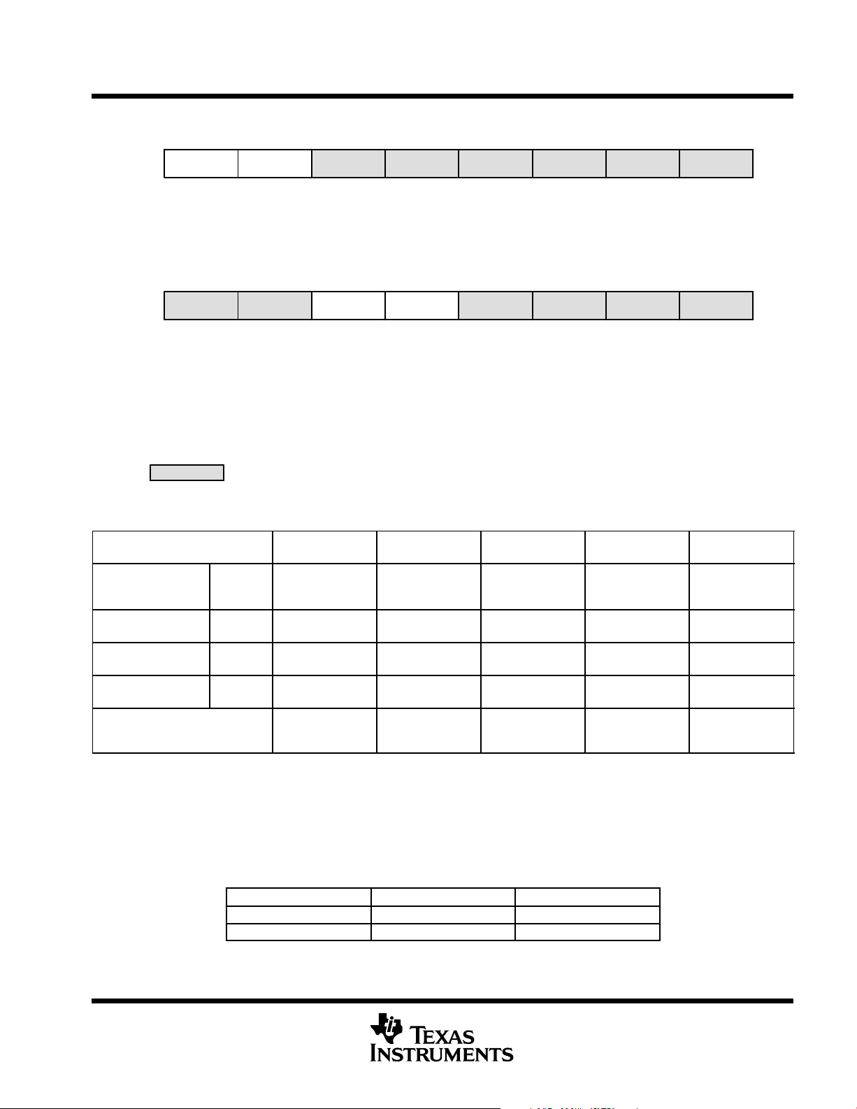
Table 1. Instruction Word Formats
Dual operands, source-destination e.g. ADD R4,R5 R4 + R5 −−−> R5
Single operands, destination only e.g. CALL R8 PC −−>(TOS), R8−−> PC
Relative jump, un/conditional e.g. JNE Jump-on-equal bit = 0
Table 2. Address Mode Descriptions
ADDRESS MODE S D SYNTAX EXAMPLE OPERATION
Register D
Indexed D D MOV X(Rn),Y(Rm) MOV 2(R5),6(R6) M(2+R5)−−> M(6+R6)
Symbolic (PC relative) D D MOV EDE,TONI M(EDE) −−> M(TONI)
Absolute D D MOV &MEM,&TCDAT M(MEM) −−> M(TCDAT)
Indirect D MOV @Rn,Y(Rm) MOV @R10,Tab(R6) M(R10) −−> M(Tab+R6)
Indirect
autoincrement
Immediate D MOV #X,TONI MOV #45,TONI #45 −−> M(TONI)
NOTE: S = source D = destination
D
D MOV @Rn+,Rm MOV @R10+,R11
MOV Rs,Rd MOV R10,R11 R10 −−> R11
M(R10) −−> R11
R10 + 2−−> R10
POST OFFICE BOX 655303 • DALLAS, TEXAS 75265
19

MSP430x43x1, MSP430x43x, MSP430x44x
MIXED SIGNAL MICROCONTROLLER
SLAS344F − JANUARY 2002 − REVISED MAY 2007
operating modes
The MSP430 has one active mode and five software selectable low-power modes of operation. An interrupt
event can wake up the device from any of the five low-power modes, service the request and restore back to
the low-power mode on return from the interrupt program.
The following six operating modes can be configured by software:
D Active mode (AM)
− All clocks are active
D Low-power mode 0 (LPM0)
− CPU is disabled
ACLK and SMCLK remain active. MCLK is disabled
FLL+ loop control remains active
D Low-power mode 1 (LPM1)
− CPU is disabled
FLL+ loop control is disabled
ACLK and SMCLK remain active. MCLK is disabled
D Low-power mode 2 (LPM2)
− CPU is disabled
MCLK, FLL+ loop control, and DCOCLK are disabled
DCO’s dc-generator remains enabled
ACLK remains active
D Low-power mode 3 (LPM3)
− CPU is disabled
MCLK, FLL+ loop control, and DCOCLK are disabled
DCO’s dc-generator is disabled
ACLK remains active
D Low-power mode 4 (LPM4)
− CPU is disabled
ACLK is disabled
MCLK, FLL+ loop control, and DCOCLK are disabled
DCO’s dc-generator is disabled
Crystal oscillator is stopped
20
POST OFFICE BOX 655303 • DALLAS, TEXAS 75265
MSP430x43x1, MSP430x43x, MSP430x44x
MIXED SIGNAL MICROCONTROLLER
SLAS344F − JANUARY 2002 − REVISED MAY 2007
interrupt vector addresses
The interrupt vectors and the power-up starting address are located in the address range 0FFFFh−0FFE0h. The
vector contains the 16-bit address of the appropriate interrupt-handler instruction sequence.
Table 3. Interrupt Sources, Flags, and Vectors of 4xx Configurations
INTERRUPT SOURCE INTERRUPT FLAG SYSTEM INTERRUPT
Power-Up
External Reset
Watchdog
Flash Memory
NMI
Oscillator Fault
Flash Memory Access Violation
Timer_B7
Timer_B7
Comparator_A CAIFG Maskable 0FFF6h 11
Watchdog Timer WDTIFG Maskable 0FFF4h 10
USART0 Receive URXIFG0 Maskable 0FFF2h 9
USART0 Transmit UTXIFG0 Maskable 0FFF0h 8
ADC12 (see Note 4) ADC12IFG (see Notes 1 and 2) Maskable 0FFEEh 7
Timer_A3 TACCR0 CCIFG (see Note 2) Maskable 0FFECh 6
Timer_A3
I/O Port P1 (Eight Flags)
USART1 Receive
USART1 Transmit
I/O Port P2 (Eight Flags)
Basic Timer1 BTIFG Maskable 0FFE0h 0, lowest
†
’43x(1) uses Timer_B3 with TBCCR0, 1 and 2 CCIFG flags, and TBIFG. ’44x uses Timer_B7 with TBCCR0 CCIFG, TBCCR1 to TBCCR6
CCIFGs, and TBIFG
‡
USART1 is implemented in ’44x only.
NOTES: 1. Multiple source flags
2. Interrupt flags are located in the module.
3. (Non)maskable: the individual interrupt-enable bit can disable an interrupt event, but the general-interrupt enable can not disable
4. ADC12 is not implemented in MSP430x43x1 devices.
†
†
‡
‡
it.
NMIIFG (see Notes 1 and 3)
OFIFG (see Notes 1 and 3)
ACCVIFG (see Notes 1 and 3)
TBCCR0 CCIFG (see Note 2) Maskable 0FFFAh 13
TBCCR1 to TBCCR6 CCIFGs
TBIFG (see Notes 1 and 2)
TACCR1 and TACCR2 CCIFGs,
TAIFG (see Notes 1 and 2)
WDTIFG
KEYV
(see Note 1)
P1IFG.0 to P1IFG.7
(see Notes 1 and 2)
URXIFG1 Maskable 0FFE6h 3
UTXIFG1 Maskable 0FFE4h 2
P2IFG.0 to P2IFG.7
(see Notes 1 and 2)
Reset 0FFFEh 15, highest
(Non)maskable
(Non)maskable
(Non)maskable
Maskable 0FFF8h 12
Maskable 0FFEAh 5
Maskable 0FFE8h 4
Maskable 0FFE2h 1
WORD
ADDRESS
0FFFCh 14
PRIORITY
POST OFFICE BOX 655303 • DALLAS, TEXAS 75265
21
MSP430x43x1, MSP430x43x, MSP430x44x
MIXED SIGNAL MICROCONTROLLER
SLAS344F − JANUARY 2002 − REVISED MAY 2007
special function registers
Most interrupt and module-enable bits are collected in the lowest address space. Special-function register bits
not allocated to a functional purpose are not physically present in the device. This arrangement provides simple
software access.
interrupt enable 1 and 2
Address
0h URXIE0 ACCVIE NMIIE
7654 0
UTXIE0 OFIE WDTIE
rw–0 rw–0 rw–0
rw–0 rw–0 rw–0
321
WDTIE: Watchdog-timer interrupt enable. Inactive if watchdog mode is selected. Active if watchdog
timer is configured in interval timer mode.
OFIE: Oscillator-fault-interrupt enable
NMIIE: Nonmaskable-interrupt enable
ACCVIE: Flash access violation interrupt enable
URXIE0: USART0: UART and SPI receive-interrupt enable
UTXIE0: USART0: UART and SPI transmit-interrupt enable
Address
01h URXIE1
7654 0
BTIE
rw–0
UTXIE1
rw–0 rw–0
321
URXIE1: USART1: UART and SPI receive-interrupt enable (MSP430F44x devices only)
UTXIE1: USART1: UART and SPI transmit-interrupt enable (MSP430F44x devices only)
BTIE: Basic timer interrupt enable
interrupt flag register 1 and 2
Address
02h URXIFG0 NMIIFG
7654 0
UTXIFG0 OFIFG WDTIFG
rw–1 rw–0
rw–0 rw–1 rw–(0)
321
WDTIFG: Set on watchdog timer overflow (in watchdog mode) or security key violation. Reset on V
power up or a reset condition at the RST/NMI pin in reset mode.
OFIFG: Flag set on oscillator fault
NMIIFG: Set via RST
/NMI pin
URXIFG0: USART0: UART and SPI receive flag
UTXIFG0: USART0: UART and SPI transmit flag
Address
03h URXIFG1
7654 0
BTIFG
rw
UTXIFG1
rw–1 rw–0
321
URXIFG1: USART1: UART and SPI receive flag (MSP430F44x devices only)
UTXIFG1: USART1: UART and SPI transmit flag (MSP430F44x devices only)
BTIFG: Basic timer flag
22
POST OFFICE BOX 655303 • DALLAS, TEXAS 75265
CC
module enable registers 1 and 2
MSP430x43x1, MSP430x43x, MSP430x44x
MIXED SIGNAL MICROCONTROLLER
SLAS344F − JANUARY 2002 − REVISED MAY 2007
Address
04h
7654 0
UTXE0
rw–0 rw–0
URXE0
USPIE0
321
URXE0: USART0: UART mode receive enable
UTXE0: USART0: UART mode transmit enable
USPIE0: USART0: SPI mode transmit and receive enable
Address
05h
7654 0
UTXE1
rw–0 rw–0
URXE1
USPIE1
321
URXE1: USART1: UART mode receive enable (MSP430F44x devices only)
UTXE1: USART1: UART mode transmit enable (MSP430F44x devices only)
USPIE1: USART1: SPI mode transmit and receive enable (MSP430F44x devices only)
Legend: rw:
rw–0,1:
rw–(0,1):
Bit Can Be Read and Written
Bit Can Be Read and Written. It Is Reset or Set by PUC.
Bit Can Be Read and Written. It Is Reset or Set by POR.
SFR Bit Not Present in Device
memory organization
MSP430F435 MSP430F436
Memory
Main: interrupt vector
Main: code memory
Information memory Size
Boot memory Size
RAM Size 512 Byte
Peripherals 16-bit
Size
Flash
Flash
Flash
ROM
8-bit
8-bit SFR
16KB
0FFFFh − 0FFE0h
0FFFFh − 0C000h
256 Byte
010FFh − 01000h
1KB
0FFFh − 0C00h
03FFh − 0200h
01FFh − 0100h
0FFh − 010h
0Fh − 00h
24KB
0FFFFh − 0FFE0h
0FFFFh − 0A000h
256 Byte
010FFh − 01000h
1KB
0FFFh − 0C00h
1KB
05FFh − 0200h
01FFh − 0100h
0FFh − 010h
0Fh − 00h
MSP430F437
MSP430F447
32KB
0FFFFh − 0FFE0h
0FFFFh − 08000h
256 Byte
010FFh − 01000h
1KB
0FFFh − 0C00h
1KB
05FFh − 0200h
01FFh − 0100h
0FFh − 010h
0Fh − 00h
MSP430F448 MSP430F449
0FFFFh − 0FFE0h
0FFFFh − 04000h
010FFh − 01000h
0FFFh − 0C00h
09FFh − 0200h
01FFh − 0100h
48KB
256 Byte
1KB
2KB
0FFh − 010h
0Fh − 00h
60KB
0FFFFh − 0FFE0h
0FFFFh − 01100h
256 Byte
010FFh − 01000h
1KB
0FFFh − 0C00h
2KB
09FFh − 0200h
01FFh − 0100h
0FFh − 010h
0Fh − 00h
bootstrap loader (BSL)
The MSP430 bootstrap loader (BSL) enables users to program the flash memory or RAM using a UART serial
interface. Access to the MSP430 memory via the BSL is protected by user-defined password. For complete
description of the features of the BSL and its implementation, see the Application report Features of the MSP430
Bootstrap Loader, Literature Number SLAA089.
BSL Function PN Package Pins PZ Package Pins
Data Transmit 67 - P1.0 87 - P1.0
Data Receive 66 - P1.1 86 - P1.1
POST OFFICE BOX 655303 • DALLAS, TEXAS 75265
23
MSP430x43x1, MSP430x43x, MSP430x44x
MIXED SIGNAL MICROCONTROLLER
SLAS344F − JANUARY 2002 − REVISED MAY 2007
flash memory
The flash memory can be programmed via the JTAG port, the bootstrap loader, or in-system by the CPU. The
CPU can perform single-byte and single-word writes to the flash memory. Features of the flash memory include:
D Flash memory has n segments of main memory and two segments of information memory (A and B) of 128
bytes each. Each segment in main memory is 512 bytes in size.
D Segments 0 to n may be erased in one step, or each segment may be individually erased.
D Segments A and B can be erased individually, or as a group with segments 0−n.
Segments A and B are also called information memory.
D New devices may have some bytes programmed in the information memory (needed for test during
manufacturing). The user should perform an erase of the information memory prior to the first use.
16KB
24KB
32KB
48KB
60KB
0FFFFh
0FE00h
0FDFFh
0FC00h
0FBFFh
0FA00h
0F9FFh
0C400h
0C3FFh
0C200h
0C1FFh
0C000h
010FFh
01080h
0107Fh
01000h
0FFFFh
0FE00h
0FDFFh
0FC00h
0FBFFh
0FA00h
0F9FFh
0A400h
0A3FFh
0A200h
0A1FFh
0A000h
010FFh
01080h
0107Fh
01000h
0FFFFh
0FE00h
0FDFFh
0FC00h
0FBFFh
0FA00h
0F9FFh
08400h
083FFh
08200h
081FFh
08000h
010FFh
01080h
0107Fh
01000h
0FFFFh
0FE00h
0FDFFh
0FC00h
0FBFFh
0FA00h
0F9FFh
04400h
043FFh
04200h
041FFh
04000h
010FFh
01080h
0107Fh
01000h
0FFFFh
0FE00h
0FDFFh
0FC00h
0FBFFh
0FA00h
0F9FFh
01400h
013FFh
01200h
011FFh
01100h
010FFh
01080h
0107Fh
01000h
Segment 0
w/ Interrupt Vectors
Segment 1
Segment 2
Main
Memory
Segment n-1
Segment n
Segment A
Information
Memory
Segment B
24
POST OFFICE BOX 655303 • DALLAS, TEXAS 75265

MSP430x43x1, MSP430x43x, MSP430x44x
MIXED SIGNAL MICROCONTROLLER
SLAS344F − JANUARY 2002 − REVISED MAY 2007
peripherals
Peripherals are connected to the CPU through data, address, and control busses and can be handled using
all instructions. For complete module descriptions, refer to the MSP430x4xx Family User’s Guide, literature
number SLAU056.
digital I/O
There are six 8-bit I/O ports implemented—ports P1 through P6:
D All individual I/O bits are independently programmable.
D Any combination of input, output, and interrupt conditions is possible.
D Edge-selectable interrupt input capability for all the eight bits of ports P1 and P2.
D Read/write access to port-control registers is supported by all instructions.
oscillator and system clock
The clock system in the MSP430x43x(1) and MSP43x44x family of devices is supported by the FLL+ module
that includes support for a 32768-Hz watch crystal oscillator, an internal digitally-controlled oscillator (DCO) and
a high frequency crystal oscillator. The FLL+ clock module is designed to meet the requirements of both low
system cost and low-power consumption. The FLL+ features a digital frequency locked loop (FLL) hardware
which in conjunction with a digital modulator stabilizes the DCO frequency to a programmable multiple of the
watch crystal frequency. The internal DCO provides a fast turn-on clock source and stabilizes in less than 6 μs.
The FLL+ module provides the following clock signals:
D Auxiliary clock (ACLK), sourced from a 32768-Hz watch crystal or a high frequency crystal.
D Main clock (MCLK), the system clock used by the CPU.
D Sub-Main clock (SMCLK), the sub-system clock used by the peripheral modules.
D ACLK/n, the buffered output of ACLK, ACLK/2, ACLK/4, or ACLK/8.
brownout, supply voltage supervisor
The brownout circuit is implemented to provide the proper internal reset signal to the device during power on
and power off. The supply voltage supervisor (SVS) circuitry detects if the supply voltage drops below a user
selectable level and supports both supply voltage supervision (the device is automatically reset) and supply
voltage monitoring (SVM, the device is not automatically reset).
The CPU begins code execution after the brownout circuit releases the device reset. However, V
have ramped to V
reaches V
. If desired, the SVS circuit can be used to determine when VCC reaches V
CC(min)
hardware multiplier (MSP430x44x Only)
The multiplication operation is supported by a dedicated peripheral module. The module performs 16 16,
16 8, 8 16, and 8 8 bit operations. The module is capable of supporting signed and unsigned multiplication
as well as signed and unsigned multiply and accumulate operations. The result of an operation can be accessed
immediately after the operands have been loaded into the peripheral registers. No additional clock cycles are
required.
watchdog timer
at that time. The user must insure the default FLL+ settings are not changed until V
CC(min)
CC(min)
may not
CC
.
CC
The primary function of the watchdog timer (WDT) module is to perform a controlled system restart after a
software problem occurs. If the selected time interval expires, a system reset is generated. If the watchdog
function is not needed in an application, the module can be configured as an interval timer and can generate
interrupts at selected time intervals.
POST OFFICE BOX 655303 • DALLAS, TEXAS 75265
25

MSP430x43x1, MSP430x43x, MSP430x44x
Device Input
Module Input
Module
Module Output
MIXED SIGNAL MICROCONTROLLER
SLAS344F − JANUARY 2002 − REVISED MAY 2007
USART0
The MSP430x43x(1) and the MSP430x44x have one hardware universal synchronous/asynchronous receive
transmit (USART0) peripheral module that is used for serial data communication. The USART supports
synchronous SPI (3 or 4 pin) and asynchronous UART communication protocols, using double-buffered
transmit and receive channels.
USART1 (MSP430x44x Only)
The MSP430x44x has a second hardware universal synchronous/asynchronous receive transmit (USART1)
peripheral module that is used for serial data communication. The USART supports synchronous SPI (3 or 4
pin) and asynchronous UART communication protocols, using double-buffered transmit and receive channels.
Operation of USART1 is identical to USART0.
timer_A3
Timer_A3 is a 16-bit timer/counter with three capture/compare registers. Timer_A3 can support multiple
capture/compares, PWM outputs, and interval timing. Timer_A3 also has extensive interrupt capabilities.
Interrupts may be generated from the counter on overflow conditions and from each of the capture/compare
registers.
Timer_A3 Signal Connections
Input Pin Number
PN PZ
62 - P1.5 82 - P1.5 TACLK TACLK
62 - P1.5 82 - P1.5 TACLK INCLK
67 - P1.0 87 - P1.0 TA0 CCI0A
66 - P1.1 86 - P1.1 TA0 CCI0B
65 - P1.2 85 - P1.2 TA1 CCI1A
59 - P2.0 79 - P2.0 TA2 CCI2A
Device Input Module Input Module Module Output
Signal
ACLK ACLK
SMCLK SMCLK
DV
SS
DV
CC
CAOUT (internal) CCI1B
DV
SS
DV
CC
ACLK (internal) CCI2B
DV
SS
DV
CC
Name
GND
V
CC
GND
V
CC
GND
V
CC
Block
Timer NA
CCR0 TA 0
CCR1 TA 1
CCR2 TA 2
Signal
Output Pin Number
PN PZ
67 - P1.0 87 - P1.0
14 - P1.2 85 - P1.2
ADC12 (internal)
15 - P1.3 79 - P2.0
timer_B3 (MSP430x43x(1) Only)
Timer_B3 is a 16-bit timer/counter with three capture/compare registers. Timer_B3 can support multiple
capture/compares, PWM outputs, and interval timing. Timer_B3 also has extensive interrupt capabilities.
Interrupts may be generated from the counter on overflow conditions and from each of the capture/compare
registers.
26
POST OFFICE BOX 655303 • DALLAS, TEXAS 75265

MSP430x43x1, MSP430x43x, MSP430x44x
Device Input
Module Input
Module
Module Output
MIXED SIGNAL MICROCONTROLLER
SLAS344F − JANUARY 2002 − REVISED MAY 2007
timer_B7 (MSP430x44x Only)
Timer_B7 is a 16-bit timer/counter with seven capture/compare registers. Timer_B7 can support multiple
capture/compares, PWM outputs, and interval timing. Timer_B7 also has extensive interrupt capabilities.
Interrupts may be generated from the counter on overflow conditions and from each of the capture/compare
registers.
Timer_B3/B7 Signal Connections
Input Pin Number
PN PZ
Device Input Module Input Module Module Output
Signal
Name
63 - P1.4 83 - P1.4 TBCLK TBCLK
ACLK ACLK
SMCLK SMCLK
63 - P1.4 83 - P1.4 TBCLK INCLK
58 - P2.1 78 - P2.1 TB0 CCI0A
58 - P2.1 78 - P2.1 TB0 CCI0B
DV
DV
SS
CC
GND
V
CC
57 - P2.2 77 - P2.2 TB1 CCI1A
57 - P2.2 77 - P2.2 TB1 CCI1B
DV
DV
SS
CC
GND
V
CC
56 - P2.3 76 - P2.3 TB2 CCI2A
56 - P2.3 76 - P2.3 TB2 CCI2B
DV
DV
SS
CC
GND
V
CC
67 - P3.4 TB3 CCI3A
67 - P3.4 TB3 CCI3B
DV
DV
SS
CC
GND
V
CC
66 - P3.5 TB4 CCI4A
66 - P3.5 TB4 CCI4B
DV
DV
SS
CC
GND
V
CC
65 - P3.6 TB5 CCI5A
65 - P3.6 TB5 CCI5B
DV
DV
SS
CC
GND
V
CC
64 - P3.7 TB6 CCI6A
ACLK (internal) CCI6B
DV
SS
DV
CC
†
Timer_B3 implements three capture/compare blocks (CCR0, CCR1 and CCR2 only).
GND
V
CC
†
Block
Signal
Timer NA
CCR0 TB0
CCR1 TB1
CCR2 TB2
CCR3 TB3
CCR4 TB4
CCR5 TB5
CCR6 TB6
Output Pin Number
PN PZ
58 - P2.1 78 - P2.1
ADC12 (internal)
57 - P2.2 77 - P2.2
ADC12 (internal)
56 - P2.3 76 - P2.3
67 - P3.4
66 - P3.5
65 - P3.6
64 - P3.7
POST OFFICE BOX 655303 • DALLAS, TEXAS 75265
27

MSP430x43x1, MSP430x43x, MSP430x44x
MIXED SIGNAL MICROCONTROLLER
SLAS344F − JANUARY 2002 − REVISED MAY 2007
comparator_A
The primary function of the comparator_A module is to support precision slope analog−to−digital conversions,
battery−voltage supervision, and monitoring of external analog signals.
ADC12 (Not implemented in the MSP430x43x1)
The ADC12 module supports fast, 12-bit analog-to-digital conversions. The module implements a 12-bit SAR
core, sample select control, reference generator and a 16 word conversion-and-control buffer. The
conversion-and-control buffer allows up to 16 independent ADC samples to be converted and stored without
any CPU intervention.
Basic Timer1
The Basic Timer1 has two independent 8-bit timers which can be cascaded to form a 16-bit timer/counter. Both
timers can be read and written by software. The Basic Timer1 can be used to generate periodic interrupts and
clock for the LCD module.
LCD drive
The LCD driver generates the segment and common signals required to drive an LCD display. The LCD
controller has dedicated data memory to hold segment drive information. Common and segment signals are
generated as defined by the mode. Static, 2-MUX, 3-MUX, and 4-MUX LCDs are supported by this peripheral.
28
POST OFFICE BOX 655303 • DALLAS, TEXAS 75265

peripheral file map
Watchdog Watchdog timer control WDTCTL 0120h
Timer_B7/
Timer_B3
(see Note 1)
Timer_A3
Hardware
Multiplier
(MSP430x44x only)
NOTE 1: Timer_B7 in the MSP430x44x family has seven CCRs; Timer_B3 in the MSP430x43x(1) family has three CCRs.
MSP430x43x1, MSP430x43x, MSP430x44x
MIXED SIGNAL MICROCONTROLLER
SLAS344F − JANUARY 2002 − REVISED MAY 2007
PERIPHERALS WITH WORD ACCESS
_
_
Capture/compare register 6 TBCCR6 019Eh
Capture/compare register 5 TBCCR5 019Ch
Capture/compare register 4 TBCCR4 019Ah
Capture/compare register 3 TBCCR3 0198h
Capture/compare register 2 TBCCR2 0196h
Capture/compare register 1 TBCCR1 0194h
Capture/compare register 0 TBCCR0 0192h
Timer_B register TBR 0190h
Capture/compare control 6 TBCCTL6 018Eh
Capture/compare control 5 TBCCTL5 018Ch
Capture/compare control 4 TBCCTL4 018Ah
Capture/compare control 3 TBCCTL3 0188h
Capture/compare control 2 TBCCTL2 0186h
Capture/compare control 1 TBCCTL1 0184h
Capture/compare control 0 TBCCTL0 0182h
Timer_B control TBCTL 0180h
Timer_B interrupt vector TBIV 011Eh
Reserved 017Eh
Reserved 017Ch
Reserved 017Ah
Reserved 0178h
Capture/compare register 2 TACCR2 0176h
Capture/compare register 1 TACCR1 0174h
Capture/compare register 0 TACCR0 0172h
Timer_A register TAR 0170h
Reserved 016Eh
Reserved 016Ch
Reserved 016Ah
Reserved 0168h
Capture/compare control 2 TACCTL2 0166h
Capture/compare control 1 TACCTL1 0164h
Capture/compare control 0 TACCTL0 0162h
Timer_A control TACTL 0160h
Timer_A interrupt vector TAIV 012Eh
Sum extend SUMEXT 013Eh
Result high word RESHI 013Ch
Result low word RESLO 013Ah
Second operand OP2 0138h
Multiply signed + accumulate/operand1 MACS 0136h
Multiply + accumulate/operand1 MAC 0134h
Multiply signed/operand1 MPYS 0132h
Multiply unsigned/operand1 MPY 0130h
POST OFFICE BOX 655303 • DALLAS, TEXAS 75265
29

MSP430x43x1, MSP430x43x, MSP430x44x
MIXED SIGNAL MICROCONTROLLER
SLAS344F − JANUARY 2002 − REVISED MAY 2007
peripheral file map (continued)
PERIPHERALS WITH WORD ACCESS (CONTINUED)
Flash
ADC12
Flash control 3 FCTL3 012Ch
Flash control 2 FCTL2 012Ah
Flash control 1 FCTL1 0128h
Conversion memory 15 ADC12MEM15 015Eh
Conversion memory 14 ADC12MEM14 015Ch
Conversion memory 13 ADC12MEM13 015Ah
Conversion memory 12 ADC12MEM12 0158h
Conversion memory 11 ADC12MEM11 0156h
Conversion memory 10 ADC12MEM10 0154h
Conversion memory 9 ADC12MEM9 0152h
Conversion memory 8 ADC12MEM8 0150h
Conversion memory 7 ADC12MEM7 014Eh
Conversion memory 6 ADC12MEM6 014Ch
Conversion memory 5 ADC12MEM5 014Ah
Conversion memory 4 ADC12MEM4 0148h
Conversion memory 3 ADC12MEM3 0146h
Conversion memory 2 ADC12MEM2 0144h
Conversion memory 1 ADC12MEM1 0142h
Conversion memory 0 ADC12MEM0 0140h
Interrupt-vector-word register ADC12IV 01A8h
Inerrupt-enable register ADC12IE 01A6h
Inerrupt-flag register ADC12IFG 01A4h
Control register 1 ADC12CTL1 01A2h
Control register 0 ADC12CTL0 01A0h
ADC memory-control register15 ADC12MCTL15 08Fh
ADC memory-control register14 ADC12MCTL14 08Eh
ADC memory-control register13 ADC12MCTL13 08Dh
ADC memory-control register12 ADC12MCTL12 08Ch
ADC memory-control register11 ADC12MCTL11 08Bh
ADC memory-control register10 ADC12MCTL10 08Ah
ADC memory-control register9 ADC12MCTL9 089h
ADC memory-control register8 ADC12MCTL8 088h
ADC memory-control register7 ADC12MCTL7 087h
ADC memory-control register6 ADC12MCTL6 086h
ADC memory-control register5 ADC12MCTL5 085h
ADC memory-control register4 ADC12MCTL4 084h
ADC memory-control register3 ADC12MCTL3 083h
ADC memory-control register2 ADC12MCTL2 082h
ADC memory-control register1 ADC12MCTL1 081h
ADC memory-control register0 ADC12MCTL0 080h
30
POST OFFICE BOX 655303 • DALLAS, TEXAS 75265

peripheral file map (continued)
p
LCD LCD memory 20
USART1
(Only in ‘x44x)
USART0
Comparator_A
BrownOUT, SVS SVS control register (Reset by brownout signal) SVSCTL 056h
FLL+ Clock
Basic Timer1 BT counter2
Port P6
Port P5
_
MSP430x43x1, MSP430x43x, MSP430x44x
MIXED SIGNAL MICROCONTROLLER
SLAS344F − JANUARY 2002 − REVISED MAY 2007
PERIPHERALS WITH BYTE ACCESS
LCDM20
:
LCD memory 16
LCD memory 15
:
LCD memory 1
LCD control and mode
Transmit buffer U1TXBUF 07Fh
Receive buffer U1RXBUF 07Eh
Baud rate U1BR1 07Dh
Baud rate U1BR0 07Ch
Modulation control U1MCTL 07Bh
Receive control U1RCTL 07Ah
Transmit control U1TCTL 079h
USART control U1CTL 078h
Transmit buffer U0TXBUF 077h
Receive buffer U0RXBUF 076h
Baud rate U0BR1 075h
Baud rate U0BR0 074h
Modulation control U0MCTL 073h
Receive control U0RCTL 072h
Transmit control U0TCTL 071h
USART control U0CTL 070h
Comparator_A port disable CAPD 05Bh
Comparator_A control2 CACTL2 05Ah
Comparator_A control1 CACTL1 059h
FLL+ Control1 FLL_CTL1 054h
FLL+ Control0 FLL_CTL0 053h
System clock frequency control SCFQCTL 052h
System clock frequency integrator SCFI1 051h
System clock frequency integrator SCFI0 050h
BT counter1
BT control
Port P6 selection P6SEL 037h
Port P6 direction P6DIR 036h
Port P6 output P6OUT 035h
Port P6 input P6IN 034h
Port P5 selection P5SEL 033h
Port P5 direction P5DIR 032h
Port P5 output P5OUT 031h
Port P5 input P5IN 030h
:
LCDM16
LCDM15
:
LCDM1
LCDCTL
BTCNT2
BTCNT1
BTCTL
0A4h
:
0A0h
09Fh
:
091h
090h
047h
046h
040h
POST OFFICE BOX 655303 • DALLAS, TEXAS 75265
31
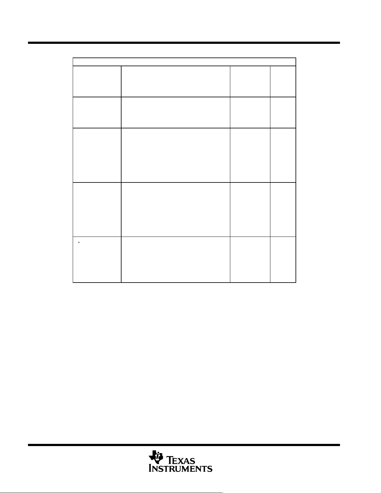
MSP430x43x1, MSP430x43x, MSP430x44x
p
MIXED SIGNAL MICROCONTROLLER
SLAS344F − JANUARY 2002 − REVISED MAY 2007
peripheral file map (continued)
PERIPHERALS WITH BYTE ACCESS (CONTINUED)
Port P4
Port P3
Port P2
Port P1
Special functions
Port P4 selection P4SEL 01Fh
Port P4 direction P4DIR 01Eh
Port P4 output P4OUT 01Dh
Port P4 input P4IN 01Ch
Port P3 selection P3SEL 01Bh
Port P3 direction P3DIR 01Ah
Port P3 output P3OUT 019h
Port P3 input P3IN 018h
Port P2 selection P2SEL 02Eh
Port P2 interrupt enable P2IE 02Dh
Port P2 interrupt-edge select P2IES 02Ch
Port P2 interrupt flag P2IFG 02Bh
Port P2 direction P2DIR 02Ah
Port P2 output P2OUT 029h
Port P2 input P2IN 028h
Port P1 selection P1SEL 026h
Port P1 interrupt enable P1IE 025h
Port P1 interrupt-edge select P1IES 024h
Port P1 interrupt flag P1IFG 023h
Port P1 direction P1DIR 022h
Port P1 output P1OUT 021h
Port P1 input P1IN 020h
SFR module enable2 ME2 005h
SFR module enable1 ME1 004h
SFR interrupt flag2 IFG2 003h
SFR interrupt flag1 IFG1 002h
SFR interrupt enable2 IE2 001h
SFR interrupt enable1 IE1 000h
absolute maximum ratings over operating free-air temperature (unless otherwise noted)
†
Voltage applied at VCC to VSS −0.3 V to 4.1 V. . . . . . . . . . . . . . . . . . . . . . . . . . . . . . . . . . . . . . . . . . . . . . . . . . . . . .
Voltage applied to any pin (see Note) −0.3 V to V
CC
+ 0.3 V. . . . . . . . . . . . . . . . . . . . . . . . . . . . . . . . . . . . . . . . . .
Diode current at any device terminal . ±2 mA. . . . . . . . . . . . . . . . . . . . . . . . . . . . . . . . . . . . . . . . . . . . . . . . . . . . . .
Storage temperature, T
: (unprogrammed device) −55°C to 150°C. . . . . . . . . . . . . . . . . . . . . . . . . . . . . . . . . .
stg
(programmed device) −40°C to 85°C. . . . . . . . . . . . . . . . . . . . . . . . . . . . . . . . . . . . .
†
Stresses beyond those listed under “absolute maximum ratings” may cause permanent damage to the device. These are stress ratings only, and
functional operation of the device at these or any other conditions beyond those indicated under “recommended operating conditions” is not
implied. Exposure to absolute-maximum-rated conditions for extended periods may affect device reliability.
NOTE: All voltages referenced to V
to the TDI/TCLK pin when blowing the JTAG fuse.
. The JTAG fuse-blow voltage, VFB, is allowed to exceed the absolute maximum rating. The voltage is applied
SS
32
POST OFFICE BOX 655303 • DALLAS, TEXAS 75265
MSP430x43x1, MSP430x43x, MSP430x44x
(see Note 3)
MIXED SIGNAL MICROCONTROLLER
SLAS344F − JANUARY 2002 − REVISED MAY 2007
recommended operating conditions
MIN NOM MAX UNITS
Supply voltage during program execution
V
(AVCC = DV
CC
CC1
= DV
= VCC) (see Note 1)
CC2
Supply voltage during program execution, SVS enabled, PORON=1
(see Note 1 and Note 2)
(AVCC = DV
V
CC
CC1
= DV
CC2
= VCC)
Supply voltage during flash memory programming
V
(AVCC = DV
CC
Supply voltage, V
Operating free-air temperature range, T
= DV
CC1
(AVSS = DV
SS
= VCC) (see Note 1)
CC2
= DV
SS1
A
= VSS) 0 0 V
SS2
LF selected,
XTS_FLL=0
LFXT1 crystal frequency, f
(see Note 3)
(LFXT1)
XT1 selected,
XTS_FLL=1
XT1 selected,
XTS_FLL=1
XT2 crystal frequency, f
Processor frequency (signal MCLK), f
(XT2)
(System)
NOTES: 1. It is recommended to power AVCC and DVCC from the same source. A maximum difference of 0.3 V between AVCC and DVCC can
be tolerated during power up and operation.
2. The minimum operating supply voltage is defined according to the trip point where POR is going active by decreasing the supply
voltage. POR is going inactive when the supply voltage is raised above the minimum supply voltage plus the hysteresis of the SVS
circuitry.
3. In LF mode, the LFXT1 oscillator requires a watch crystal. In XT1 mode, LFXT1 accepts a ceramic resonator or a crystal.
MSP430F43x(1),
MSP430F44x
MSP430F43x(1),
MSP430F44x
MSP430F43x(1),
MSP430F44x
MSP430x43x(1),
MSP430x44x
1.8 3.6 V
2 3.6 V
2.7 3.6 V
−40 85 °C
Watch crystal 32.768 kHz
Ceramic resonator 450 8000 kHz
Crystal 1000 8000 kHz
Ceramic resonator 450 8000
Crystal 1000 8000
VCC = 1.8 V DC 4.15
VCC = 3.6 V DC 8
kHz
MHz
f
(MHz)
System
8 MHz
Supply voltage range,
’F43x(1)/’F44x, during
program execution
Supply voltage range, ’F43x(1)/’F44x,
during flash memory programming
4.15 MHz
1.8 3.62.7 3
Supply Voltage − V
Figure 1. Frequency vs Supply Voltage, MSP430F43x(1) or MSP430F44x
POST OFFICE BOX 655303 • DALLAS, TEXAS 75265
33
MSP430x43x1, MSP430x43x, MSP430x44x
f
(MCLK)
f
(SMCLK)
MHz
Low power mode, (LPM0)
(
f(MCLK) = f (SMCLK) = 0 MHz
f
(ACLK)
768 Hz, SCG0 = 1
()
L
(LPM4)
f
(MCLK)
MHz, f
(SMCLK)
MHz
(ACLK)
MIXED SIGNAL MICROCONTROLLER
SLAS344F − JANUARY 2002 − REVISED MAY 2007
electrical characteristics over recommended operating free-air temperature (unless otherwise
noted)
supply current into AVCC + DVCC excluding external current
PARAMETER TEST CONDITIONS MIN NOM MAX UNIT
Active mode, (see Note 1)
I
(AM)
f
(ACLK)
= f
=
= 32,768 Hz
= 1 MHz,
= 1
f
XTS_FLL=0, SELM=(0,1)
I
(LPM0)
Low-power mode, (LPM0)
(see Note 1 and Note 4)
Low-power mode, (LPM2),
f
I
(LPM2)
MCLK) = f (SMCLK) = 0 MHz,
f(ACLK) = 32,768 Hz, SCG0 = 0 (see Note 2 and
Note 4)
Low-power mode, (LPM3)
f
I
(LPM3)
= f
(MCLK)
= 32,768 Hz, SCG0 = 1
= 32,
f
(see Note 3 and Note 4)
(SMCLK)
= 0 MHz,
ow-power mode,
f
= 0 MHz, f
I
(LPM4)
= 0
= 0 Hz, SCG0 = 1
f
(ACLK)
(see Note 2 and Note 4)
NOTES: 1. Timer_B is clocked by f
2. All inputs are tied to 0 V or to V
3. All inputs are tied to 0 V or to V
active Basic Timer1 and LCD (ACLK selected). The current consumption of the Comparator_A and the SVS module are specified
in the respective sections. The LPM3 currents are characterized with a KDS Daishinku DT−38 (6 pF) crystal and OSCCAPx=1h.
4. Current consumption for brownout included.
,
,
= 0 MHz,
= 0
(DCOCLK)
T
= −40°C to 85°C
A
= −40°C to 85°C
T
A
T
= −40°C to 85°C
A
TA = −40°C 1 1.5
TA = 25°C
TA = 60°C
TA = 85°C 3.5 6
= −40°C 1.8 2.2
T
A
TA = 25°C
TA = 60°C
TA = 85°C 4.2 7.5
TA = −40°C 0.1 0.5
TA = 25°C
TA = 60°C
T
= 85°C 1.7 3
,
A
TA = −40°C 0.1 0.5
= 25°C
T
A
TA = 60°C
TA = 85°C 1.9 3.5
= f
= 1 MHz. All inputs are tied to 0 V or to VCC. Outputs do not source or sink any current.
(DCO)
. Outputs do not source or sink any current.
CC
. Outputs do not source or sink any current. The current consumption in LPM3 is measured with
CC
VCC = 2.2 V 280 350
VCC = 3 V 420 560
VCC = 2.2 V 32 45
VCC = 3 V 55 70
VCC = 2.2 V 11 14
VCC = 3 V 17 22
VCC = 2.2 V
VCC = 3 V
VCC = 2.2 V
VCC = 3 V
1.1 1.5
2 3
1.6 1.9
2.5 3.5
0.1 0.5
0.7 1.1
0.1 0.5
0.8 1.2
μA
μA
μA
μA
μA
μA
μA
Current consumption of active mode versus system frequency
I
(AM)
= I
[1 MHz] × f
(AM)
Current consumption of active mode versus supply voltage
= I
I
(AM)
34
(AM) [3 V]
+ 175 μA/V × (V
(System)
[MHz]
– 3 V)
CC
POST OFFICE BOX 655303 • DALLAS, TEXAS 75265
MSP430x43x1, MSP430x43x, MSP430x44x
(int)
pg
for the interrupt flag, (see Note 1)
Timer_A, Timer_B clock
Leakage
MIXED SIGNAL MICROCONTROLLER
SLAS344F − JANUARY 2002 − REVISED MAY 2007
electrical characteristics over recommended operating free-air temperature (unless otherwise
noted) (continued)
SCHMITT-trigger inputs − ports P1, P2, P3, P4, P5, and P6
PARAMETER TEST CONDITIONS MIN TYP MAX UNIT
V
IT+
V
IT−
V
hys
Positive-going input threshold voltage
Negative-going input threshold voltage
Input voltage hysteresis (V
IT+
− V
IT−
)
standard inputs − RST/NMI; JTAG: TCK, TMS, TDI/TCLK
PARAMETER TEST CONDITIONS MIN TYP MAX UNIT
V
Low-level input voltage
IL
V
High-level input voltage
IH
inputs Px.x, TAx, TBx
PARAMETER TEST CONDITIONS V
t
(int)
t
(cap)
f
(TAext)
f
(TBext)
f
(TAint)
f
(TBint)
External interrupt timing
Timer_A, Timer_B capture
timing
Timer_A, Timer_B clock
frequency externally applied
to pin
Timer_A, Timer_B clock
frequency
NOTES: 1. The external signal sets the interrupt flag every time the minimum t
trigger signals shorter than t
MCLK cycles.
2. Seven capture/compare registers in ’x44x and three capture/compare registers in ’x43x(1).
Port P1, P2: P1.x to P2.x, external trigger signal
TA0, TA1, TA2 2.2 V 62
TB0, TB1, TB2, TB3, TB4, TB5, TB6
(see Note 2)
TACLK, TBCLK, INCLK: t
(H)
= t
SMCLK or ACLK signal selected
. Both the cycle and timing specifications must be met to ensure the flag is set. t
(int)
VCC = 2.2 V 1.1 1.5
V
= 3 V 1.5 1.9
CC
VCC = 2.2 V 0.4 0.9
V
= 3 V 0.9 1.3
CC
VCC = 2.2 V 0.3 1.1
VCC = 3 V 0.5 1
VCC = 2.2 V / 3 V
CC
V
SS
0.8×V
CC
MIN TYP MAX UNIT
VSS+0.6 V
2.2 V/3 V 1.5 cycle
2.2 V 62
3 V 50
3 V 50
2.2 V 8
(L)
3 V 10
2.2 V 8
3 V 10
cycle and time parameters are met. It may be set even with
(int)
(int)
V
V
V
V
CC
V
ns
ns
MHz
MHz
is measured in
leakage current (see Notes 1 and 2)
I
lkg(P1.x)
I
lkg(P2.x)
I
lkg(P3.x)
I
lkg(P4.x)
I
lkg(P5.x)
I
lkg(P6.x)
NOTES: 1. The leakage current is measured with VSS or VCC applied to the corresponding pin(s), unless otherwise noted.
2. The port pin must be selected as input and there must be no optional pullup or pulldown resistor.
PARAMETER TEST CONDITIONS MIN TYP MAX UNIT
Leakage current
Port P1 Port 1: V
Port P2 Port 2: V
Port P3 Port 3: V
Port P4 Port 4: V
Port P5 Port 5: V
Port P6 Port 6: V
(P1.x)
(P2.x)
(P3.x)
(P4.x)
(P5.x)
(P6.x)
POST OFFICE BOX 655303 • DALLAS, TEXAS 75265
VCC = 2.2 V/3 V
±50
±50
±50
±50
±50
±50
nA
35
MSP430x43x1, MSP430x43x, MSP430x44x
C
L
(Sy
)
ACLK P1.4/TBCLK/SMCLK
C
L
pF
f
(System)
MHz
P1.5/TACLK/ACLK
C
L
pF
,
P1.1/TA0/MCLK
,
P1.4/TBCLK/SMCLK
MIXED SIGNAL MICROCONTROLLER
SLAS344F − JANUARY 2002 − REVISED MAY 2007
electrical characteristics over recommended operating free-air temperature (unless otherwise
noted) (continued)
outputs − ports P1, P2, P3, P4, P5, and P6
PARAMETER TEST CONDITIONS MIN TYP MAX UNIT
V
V
High-level output voltage
OH
Low-level output voltage
OL
NOTES: 1. The maximum total current, I
specified voltage drop.
2. The maximum total current, I
specified voltage drop.
output frequency
PARAMETER TEST CONDITIONS MIN TYP MAX UNIT
f
(Px.y)
f
(ACLK)
f
(MCLK)
f
(SMCLK)
t
(Xdc)
(1 ≤ x ≤ 6, 0 ≤ y ≤ 7)
P1.1/TA0/MCLK, P1.5/TACLK/
Duty cycle of output frequency
I
I
I
I
I
I
I
I
= −1.5 mA, V
OH(max)
= −6 mA, V
OH(max)
= −1.5 mA, V
OH(max)
= −6 mA, V
OH(max)
= 1.5 mA, V
OL(max)
= 6 mA, V
OL(max)
= 1.5 mA, V
OL(max)
= 6 mA, V
OL(max)
and I
OH(max)
OH(max)
OL(max),
and I
OL(max),
CL = 20 pF,
= 20 pF,
I
= ±1.5 mA
L
CL = 20 pF f
20
C
= 20 pF
20
L
VCC = 2.2 V / 3 V
P1.1/TA0/MCLK
C
= 20 pF,
L
= 2.2 V / 3 V
V
CC
P1.4/TBCLK/SMCLK
C
= 20 pF,
L
= 2.2 V / 3 V
V
CC
= 2.2 V, See Note 1 VCC−0.25 V
CC
= 2.2 V, See Note 2 VCC−0.6 V
CC
= 3 V, See Note 1 VCC−0.25 V
CC
= 3 V, See Note 2 VCC−0.6 V
CC
= 2.2 V, See Note 1 V
CC
= 2.2 V, See Note 2 V
CC
= 3 V, See Note 1 V
CC
= 3 V, See Note 2 V
CC
SS
SS
SS
SS
CC
CC
CC
CC
VSS+0.25
VSS+0.6
VSS+0.25
VSS+0.6
V
V
for all outputs combined, should not exceed ±12 mA to satisfy the maximum
for all outputs combined, should not exceed ±48 mA to satisfy the maximum
V
= 2.2 V DC 5
CC
V
= 3 V DC 7.5
CC
f
= f
(ACLK)
,
f
= f
(ACLK)
f
= f
(ACLK)
f
= f
,
(MCLK)
f
(MCLK)
f
(SMCLK)
f
(SMCLK)
= f
,
(LFXT1)
(LFXT1)
(LFXT1)
(XT1)
(DCOCLK)
= f
(XT2)
= f
(DCOCLK)
= f
= f
(XT1)
(LF)
40% 60%
30% 70%
50%
40% 60%
50%−
15 ns
50%
50%+
15 ns
40% 60%
50%−
15 ns
50%
50%+
15 ns
stem
MHz
MHz
36
POST OFFICE BOX 655303 • DALLAS, TEXAS 75265
MSP430x43x1, MSP430x43x, MSP430x44x
MIXED SIGNAL MICROCONTROLLER
SLAS344F − JANUARY 2002 − REVISED MAY 2007
electrical characteristics over recommended operating free-air temperature (unless otherwise
noted) (continued)
outputs − Ports P1, P2, P3, P4, P5, and P6 (continued)
TYPICAL LOW-LEVEL OUTPUT CURRENT
vs
LOW-LEVEL OUTPUT VOLTAGE
16
VCC = 2.2 V
P2.7
14
12
10
8
6
4
− Typical Low-level Output Current − mA
2
OL
I
0
0.0 0.5 1.0 1.5 2.0 2.5
VOL − Low-Level Output Voltage − V
TA = 25°C
TA = 85°C
Figure 2
TYPICAL LOW-LEVEL OUTPUT CURRENT
vs
LOW-LEVEL OUTPUT VOLTAGE
25
VCC = 3 V
P2.7
20
15
10
5
− Typical Low-level Output Current − mA
OL
I
0
0.0 0.5 1.0 1.5 2.0 2.5 3.0 3.5
VOL − Low-Level Output Voltage − V
TA = 25°C
TA = 85°C
Figure 3
TYPICAL HIGH-LEVEL OUTPUT CURRENT
vs
HIGH-LEVEL OUTPUT VOLTAGE
0
VCC = 2.2 V
P2.7
−2
−4
−6
−8
−10
TA = 85°C
−12
− Typical High-level Output Current − mA
OL
I
−14
0.0 0.5 1.0 1.5 2.0 2.5
TA = 25°C
VOH − High-Level Output Voltage − V
Figure 4
TYPICAL HIGH-LEVEL OUTPUT CURRENT
vs
HIGH-LEVEL OUTPUT VOLTAGE
0
VCC = 3 V
P2.7
−5
−10
−15
−20
−25
− Typical High-level Output Current − mA
OL
I
−30
TA = 85°C
TA = 25°C
0.0 0.5 1.0 1.5 2.0 2.5 3.0 3.5
VOH − High-Level Output Voltage − V
Figure 5
POST OFFICE BOX 655303 • DALLAS, TEXAS 75265
37
MSP430x43x1, MSP430x43x, MSP430x44x
)
t
d(LPM3)
Delay time
V
CC
2.2 V/3 V
μs
pg
Segment line
MIXED SIGNAL MICROCONTROLLER
SLAS344F − JANUARY 2002 − REVISED MAY 2007
electrical characteristics over recommended operating free-air temperature (unless otherwise
noted) (continued)
wake-up LPM3
PARAMETER TEST CONDITIONS MIN TYP MAX UNIT
f = 1 MHz 6
t
d(LPM3
Delay time
f = 2 MHz
V
CC
= 2.2 V/3 V
f = 3 MHz
RAM
PARAMETER TEST CONDITIONS MIN TYP MAX UNIT
VRAMh CPU halted (see Note 1) 1.6 V
NOTE 1: This parameter defines the minimum supply voltage when the data in program memory RAM remain unchanged. No program execution
should take place during this supply voltage condition.
LCD
PARAMETER TEST CONDITIONS MIN TYP MAX UNIT
V
(33)
V
(23)
V
(13)
V
(33)
I
(R03)
I
(R13)
I
(R23)
V
(Sxx0)
V
(Sxx1)
V
(Sxx2)
V
(Sxx3)
− V
Analog voltage
(03)
Input leakage
Segment line
voltage
Voltage at P5.7/R33 2.5 VCC + 0.2
Voltage at P5.6/R23
Voltage at P5.5/R13
VCC = 3 V
[V
(33)−V(03)
[V
(33)−V(03)
] × 2/3 + V
] × 1/3 + V
(03)
(03)
Voltage at R33 to R03 2.5 VCC + 0.2
R03 = V
SS
P5.5/R13 = VCC/3
P5.6/R23 = 2 × VCC/3
I
= −3 μA, VCC = 3 V
(Sxx)
No load at all
segment and
common lines,
V
= 3 V
CC
V
(03)
V
(13)
V
(23)
V
(33)
V
(03)
V
(13)
V
(23)
V
(33)
±20
±20
±20
− 0.1
− 0.1
− 0.1
+ 0.1
6
μs
6
V
nA
V
38
POST OFFICE BOX 655303 • DALLAS, TEXAS 75265
MSP430x43x1, MSP430x43x, MSP430x44x
CAON=1
CARSEL=0, CAREF=1/2/3
T
A
25 C
T
A
25 C
T
A
25 C
T
A
25 C
MIXED SIGNAL MICROCONTROLLER
SLAS344F − JANUARY 2002 − REVISED MAY 2007
electrical characteristics over recommended operating free-air temperature (unless otherwise
noted) (continued)
Comparator_A (see Note 1)
PARAMETER TEST CONDITIONS MIN TYP MAX UNIT
I
(CC)
I
(Refladder/RefDiode)
V
(Ref025)
V
(Ref050)
Voltage @ 0.25 VCCnode
Voltage @ 0.5 VCCnode
V
CC
V
CC
CAON=1, CARSEL=0, CAREF=0
CAON=1, CARSEL=0, CAREF=1/2/3,
,
No load at P1.6/CA0 and P1.7/CA1
PCA0=1, CARSEL=1, CAREF=1,
No load at P1.6/CA0 and P1.7/CA1
PCA0=1, CARSEL=1, CAREF=2,
No load at P1.6/CA0 and P1.7/CA1
PCA0=1, CARSEL=1, CAREF=3,
V
(RefVT)
V
IC
Vp−V
V
hys
See Figure 6 and Figure 7
Common-mode input
voltage range
Offset voltage See Note 2 VCC = 2.2 V / 3 V −30 30 mV
S
Input hysteresis CAON = 1 VCC = 2.2 V / 3 V 0 0.7 1.4 mV
No load at P1.6/CA0 and P1.7/CA1;
= 85°C
T
A
CAON=1 VCC = 2.2 V / 3 V 0 VCC−1 V
TA = 25°C,
=
,
Overdrive 10 mV, without filter: CAF = 0
t
(response LH)
TA = 25°C
=
Overdrive 10 mV, with filter: CAF = 1
TA = 25°C
=
Overdrive 10 mV, without filter: CAF = 0
t
(response HL)
TA = 25°C,
=
,
Overdrive 10 mV, with filter: CAF = 1
NOTES: 1. The leakage current for the Comparator_A terminals is identical to I
2. The input offset voltage can be cancelled by using the CAEX bit to invert the Comparator_A inputs on successive measurements.
The two successive measurements are then summed together.
VCC = 2.2 V 25 40
VCC = 3 V 45 60
VCC = 2.2 V 30 50
,
VCC = 3 V 45 71
VCC = 2.2 V / 3 V 0.23 0.24 0.25
VCC = 2.2V / 3 V 0.47 0.48 0.5
VCC = 2.2 V 390 480 540
VCC = 3 V 400 490 550
VCC = 2.2 V 160 210 300
VCC = 3 V 80 150 240
VCC = 2.2 V 1.4 1.9 3.4
VCC = 3 V 0.9 1.5 2.6
VCC = 2.2 V 130 210 300
VCC = 3 V 80 150 240
VCC = 2.2 V 1.4 1.9 3.4
VCC = 3 V 0.9 1.5 2.6
specification.
lkg(Px.x)
μA
μA
mV
ns
μs
ns
μs
POST OFFICE BOX 655303 • DALLAS, TEXAS 75265
39
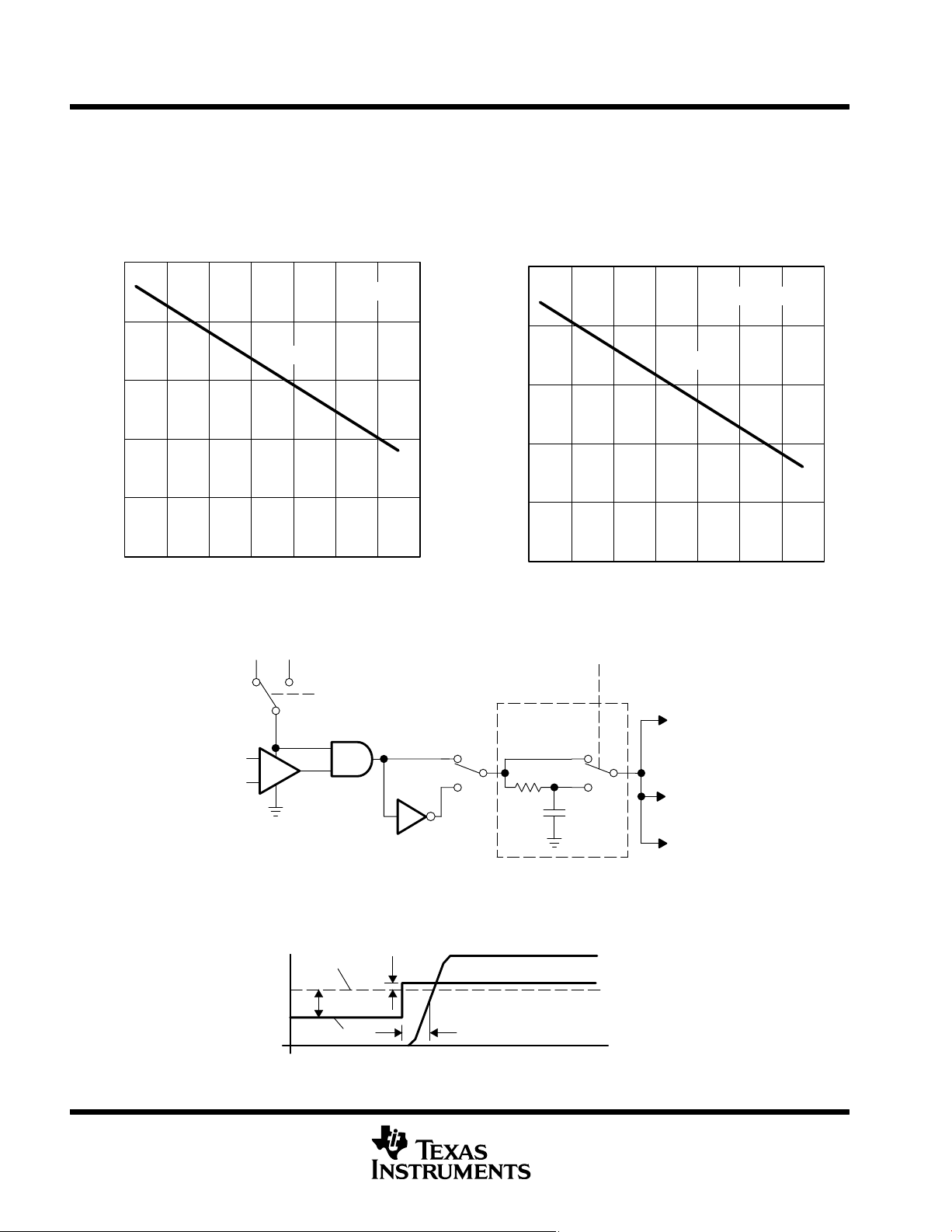
MSP430x43x1, MSP430x43x, MSP430x44x
(
)
(
)
MIXED SIGNAL MICROCONTROLLER
SLAS344F − JANUARY 2002 − REVISED MAY 2007
electrical characteristics over recommended operating free-air temperature (unless otherwise
noted) (continued)
typical characteristics
REFERENCE VOLTAGE
vs
FREE-AIR TEMPERATURE
650
VCC = 3 V
600
Typical
550
500
− Reference Voltage − mV
REF
450
V
400
−45 −25 −5 15 35 55 75 95
TA − Free-Air Temperature − °C
Figure 6. V
vs Temperature
RefVT
V
0 V
0
+
V+
_
V−
CC
1
CAON
0
1
REFERENCE VOLTAGE
vs
FREE-AIR TEMPERATURE
650
VCC = 2.2 V
600
Typical
550
500
− Reference Voltage − mV
REF
450
V
400
−45 −25 −5 15 35 55 75 95
TA − Free-Air Temperature − °C
Figure 7. V
CAF
Low-Pass Filter
0
1
vs Temperature
RefVT
To Internal
Modules
CAOUT
40
Set CAIFG
Flag
τ ≈ 2 μs
Figure 8. Block Diagram of Comparator_A Module
V
CAOUT
V−
400 mV
V+
Overdrive
t
(response)
Figure 9. Overdrive Definition
POST OFFICE BOX 655303 • DALLAS, TEXAS 75265
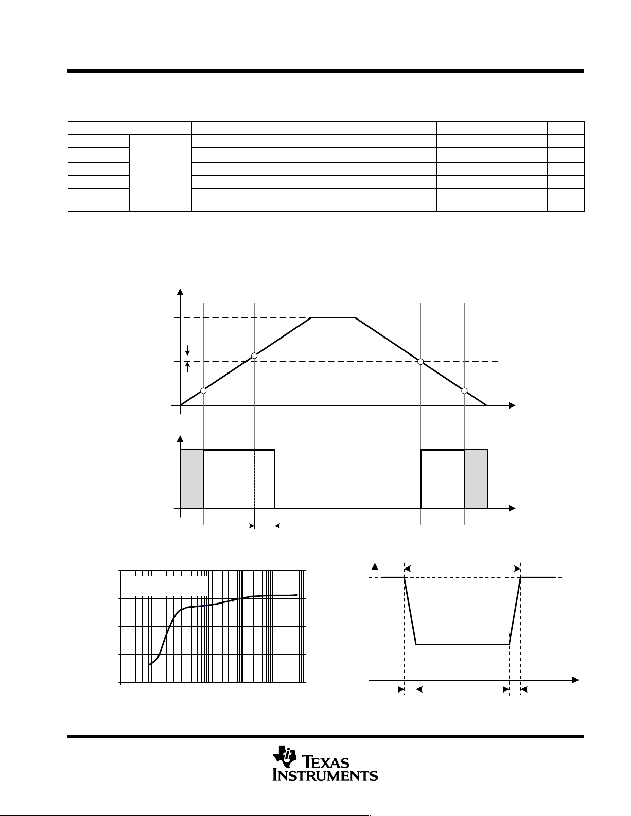
MSP430x43x1, MSP430x43x, MSP430x44x
MIXED SIGNAL MICROCONTROLLER
SLAS344F − JANUARY 2002 − REVISED MAY 2007
electrical characteristics over recommended operating free-air temperature (unless otherwise
noted) (continued)
POR/brownout reset (BOR) (see Note 1)
PARAMETER TEST CONDITIONS MIN TYP MAX UNIT
t
d(BOR)
V
CC(start)
V
(B_IT−)
V
hys(B_IT−)
t
(reset)
Brownout
(see Note 2)
dVCC/dt ≤ 3 V/s (see Figure 10) 0.7 × V
dVCC/dt ≤ 3 V/s (see Figure 10 through Figure 12) 1.71 V
dVCC/dt ≤ 3 V/s (see Figure 10) 70 130 180 mV
Pulse length needed at RST/NMI pin to accepted reset internally,
V
= 2.2 V/3 V
CC
2 μs
NOTES: 1. The current consumption of the brownout module is already included in the ICC current consumption data. The voltage level
V
+ V
(B_IT−)
hys(B_IT−)
2. During power up, the CPU begins code execution following a period of t
settings must not be changed until V
is ≤ 1.8V.
CC
≥ V
CC(min)
, where V
after VCC = V
d(BOR)
is the minimum supply voltage for the desired
CC(min)
(B_IT−)
+ V
hys(B_IT−)
operating frequency. See the MSP430x4xx Family User’s Guide (SLAU056) for more information on the brownout/SVS circuit.
typical characteristics
V
CC
2000 μs
(B_IT−)
. The default FLL+
V
1.5
− V
CC(drop)
V
0.5
V
(B_IT−)
V
CC(start)
2
= 3 V
V
CC
Typical Conditions
1
V
hys(B_IT−)
1
0
t
d(BOR)
Figure 10. POR/Brownout Reset (BOR) vs Supply Voltage
V
CC
3 V
V
CC(drop)
t
pw
0
0.001 1 1000
tpw − Pulse Width − μst
Figure 11. V
CC(drop)
Level With a Square Voltage Drop to Generate a POR/Brownout Signal
POST OFFICE BOX 655303 • DALLAS, TEXAS 75265
1 ns 1 ns
− Pulse Width − μs
pw
41

MSP430x43x1, MSP430x43x, MSP430x44x
)
V
hys(SVS_IT−)
V
V
MIXED SIGNAL MICROCONTROLLER
SLAS344F − JANUARY 2002 − REVISED MAY 2007
typical characteristics (Continued)
V
CC
2
= 3 V
V
CC
Typical Conditions
1.5
3 V
− V
1
CC(drop)
V
0.5
0
0.001 1 1000
t
− Pulse Width − μs
pw
Figure 12. V
CC(drop)
Level With a Triangle Voltage Drop to Generate a POR/Brownout Signal
V
CC(drop)
electrical characteristics over recommended operating free-air temperature (unless otherwise
noted) (continued)
SVS (supply voltage supervisor/monitor)
PARAMETER TEST CONDITIONS MIN NOM MAX UNIT
t
(SVSR)
t
d(SVSon)
t
settle
V
(SVSstart)
V
hys(SVS_IT−
(SVS_IT−)
I
CC(SVS)
(see Note 1)
†
The recommended operating voltage range is limited to 3.6 V.
‡
t
is the settling time that the comparator o/p needs to have a stable level after VLD is switched VLD ≠ 0 to a different VLD value somewhere
settle
between 2 and 15. The overdrive is assumed to be > 50 mV.
NOTE 1: The current consumption of the SVS module is not included in the I
dVCC/dt > 30 V/ms (see Figure 13) 5 150 μs
dVCC/dt ≤ 30 V/ms 2000 μs
SVSon, switch from VLD=0 to VLD ≠ 0, VCC = 3 V 20 150 μs
‡
VLD ≠ 0
VLD ≠ 0, VCC/dt ≤ 3 V/s (see Figure 13) 1.55 1.7 V
VLD = 1 70 120 155 mV
VCC/dt ≤ 3 V/s (see Figure 13)
VCC/dt ≤ 3 V/s (see Figure 13), external voltage applied
on A7
VLD = 2 .. 14
VLD = 15 4.4 10.4 mV
VLD = 1 1.8 1.9 2.05
VLD = 2 1.94 2.1 2.25
VLD = 3 2.05 2.2 2.37
VLD = 4 2.14 2.3 2.48
VLD = 5 2.24 2.4 2.6
VLD = 6 2.33 2.5 2.71
VCC/dt ≤ 3 V/s (see Figure 13)
VLD = 7 2.46 2.65 2.86
VLD = 8 2.58 2.8 3
VLD = 9 2.69 2.9 3.13
VLD = 10 2.83 3.05 3.29
VLD = 11 2.94 3.2 3.42
VLD = 12 3.11 3.35 3.61
VLD = 13 3.24 3.5 3.76
VLD = 14 3.43 3.7
VCC/dt ≤ 3 V/s (see Figure 13), external voltage applied
on A7
VLD = 15 1.1 1.2 1.3
VLD ≠ 0, VCC = 2.2 V/3 V 10 15 μA
current consumption data.
CC
t
pw
t
= t
f
r
t
f
t
r
tpw − Pulse Width − μs
V
(SVS_IT−)
× 0.004
†
12 μs
V
(SVS_IT−)
× 0.008
†
†
†
3.99
42
POST OFFICE BOX 655303 • DALLAS, TEXAS 75265

typical characteristics
V
V
(SVS_IT−)
V
(SVSstart)
V
(B_IT−)
V
CC(start)
Brownout
SVS
CC
1
0
Out
1
V
hys(SVS_IT−)
V
hys(B_IT−)
Brownout
Region
t
d(BOR)
MSP430x43x1, MSP430x43x, MSP430x44x
MIXED SIGNAL MICROCONTROLLER
Software Sets VLD>0:
SVS is Active
SVS Circuit is Active From VLD > to VCC < V(
SLAS344F − JANUARY 2002 − REVISED MAY 2007
Brown-
Out
Region
t
B_IT−)
d(BOR)
Set POR
1.5
− V
CC(drop)
V
0.5
0
1
undefined
0
t
d(SVSon)
Figure 13. SVS Reset (SVSR) vs Supply Voltage
2
Rectangular Drop
Triangular Drop
1
0
1 10 1000
− Pulse Width − μs
t
pw
100
V
V
CC(drop)
V
V
CC(drop)
CC
3 V
CC
3 V
t
d(SVSR)
t
pw
1 ns 1 ns
t
pw
Figure 14. V
CC(drop)
t
= t
f
r
t
f
t − Pulse Width − μs
t
r
With a Square Voltage Drop and a Triangle Voltage Drop to Generate an SVS Signal
POST OFFICE BOX 655303 • DALLAS, TEXAS 75265
43

MSP430x43x1, MSP430x43x, MSP430x44x
FN_8=FN_4=FN_3=0, FN_2=1; DCOPLUS = 1
Step size between adjacent DCO taps:
t
(DCO)
DtTemperature drift, N
(DCO)
01Eh, FN_8=FN_4=FN_3=FN_2=0
MIXED SIGNAL MICROCONTROLLER
SLAS344F − JANUARY 2002 − REVISED MAY 2007
electrical characteristics over recommended operating free-air temperature (unless otherwise
noted) (continued)
DCO
PARAMETER TEST CONDITIONS MIN TYP MAX UNIT
N
=01Eh, FN_8=FN_4=FN_3=FN_2=0, D = 2; DCOPLUS= 0,
f
(DCOCLK)
f
(DCO=2)
f
(DCO=27)
f
(DCO=2)
f
(DCO=27)
f
(DCO=2)
f
(DCO=27)
f
(DCO=2)
f
(DCO=27)
f
(DCO=2)
f
(DCO=27)
S
n
D
D
V
(DCO)
f
= 32.768 kHz
Crystal
FN_8=FN_4=FN_3=FN_2=0; DCOPLUS = 1
FN_8=FN_4=FN_3=FN_2=0; DCOPLUS = 1
FN_8=FN_4=FN_3=0, FN_2=1; DCOPLUS = 1
FN_8=FN_4=FN_3=0, FN_2=1; DCOPLUS = 1
FN_8=FN_4=0, FN_3= 1, FN_2=x; DCOPLUS = 1
FN_8=FN_4=0, FN_3= 1, FN_2=x; DCOPLUS = 1
FN_8=0, FN_4= 1, FN_3= FN_2=x; DCOPLUS = 1
FN_8=0, FN_4=1, FN_3= FN_2=x; DCOPLUS = 1
FN_8=1, FN_4=FN_3=FN_2=x; DCOPLUS = 1
FN_8=1,FN_4=FN_3=FN_2=x; DCOPLUS = 1
Step size between adjacent DCO taps:
Sn = f
DCO(Tap n+1)
Temperature drift, N
/ f
DCO(Tap n)
, (see Figure 16 for taps 21 to 27)
= 01Eh, FN_8=FN_4=FN_3=FN_2=0
=
D = 2; DCOPLUS = 0
Drift with VCC variation, N
(DCO)
= 01Eh,
FN_8=FN_4=FN_3=FN_2=0, D= 2; DCOPLUS = 0
VCC = 2.2 V/3 V 1 MHz
VCC = 2.2 V 0.3 0.65 1.25
VCC = 3 V 0.3 0.7 1.3
VCC = 2.2 V 2.5 5.6 10.5
VCC = 3 V 2.7 6.1 11.3
VCC = 2.2 V 0.7 1.3 2.3
VCC = 3 V 0.8 1.5 2.5
VCC = 2.2 V 5.7 10.8 18
VCC = 3 V 6.5 12.1 20
VCC = 2.2 V 1.2 2 3
VCC = 3 V 1.3 2.2 3.5
VCC = 2.2 V 9 15.5 25
VCC = 3 V 10.3 17.9 28.5
VCC = 2.2 V 1.8 2.8 4.2
VCC = 3 V 2.1 3.4 5.2
VCC = 2.2 V 13.5 21.5 33
VCC = 3 V 16 26.6 41
VCC = 2.2 V 2.8 4.2 6.2
VCC = 3 V 4.2 6.3 9.2
VCC = 2.2 V 21 32 46
VCC = 3 V 30 46 70
MHz
MHz
MHz
MHz
MHz
MHz
MHz
MHz
MHz
MHz
1 < TAP ≤ 20 1.06 1.11
TAP = 27 1.07 1.17
VCC = 2.2 V –0.2 –0.3 –0.4
VCC = 3 V –0.2 –0.3 –0.4
%/_C
VCC = 2.2 V/3 V 0 5 15 %/V
f
(DCO)
f
(DCO3V)
1.0
1.8 3.02.4 3.6
Figure 15. DCO Frequency vs Supply Voltage VCC and vs Ambient Temperature
44
f
(DCO)
f
(DCO205C)
POST OFFICE BOX 655303 • DALLAS, TEXAS 75265
1.0
20 6040 85
0−20−400
TA − °CVCC − V

MSP430x43x1, MSP430x43x, MSP430x44x
MIXED SIGNAL MICROCONTROLLER
SLAS344F − JANUARY 2002 − REVISED MAY 2007
electrical characteristics over recommended operating free-air temperature (unless otherwise
noted) (continued)
1.17
(DCO)
f
- Stepsize Ratio between DCO Taps
n
S
1.11
1.07
1.06
Max
Min
12720
DCO Tap
Figure 16. DCO Tap Step Size
Legend
Tolerance at Tap 27
DCO Frequency
Adjusted by Bits
29 to 25 in SCFI1 {N
Tolerance at Tap 2
(DCO)
}
FN_2=0
FN_3=0
FN_4=0
FN_8=0
Overlapping DCO Ranges:
uninterrupted frequency range
FN_2=1
FN_3=0
FN_4=0
FN_8=0
FN_2=x
FN_3=1
FN_4=0
FN_8=0
FN_2=x
FN_3=x
FN_4=1
FN_8=0
FN_2=x
FN_3=x
FN_4=x
FN_8=1
Figure 17. Five Overlapping DCO Ranges Controlled by FN_x Bits
POST OFFICE BOX 655303 • DALLAS, TEXAS 75265
45

MSP430x43x1, MSP430x43x, MSP430x44x
MIXED SIGNAL MICROCONTROLLER
SLAS344F − JANUARY 2002 − REVISED MAY 2007
electrical characteristics over recommended operating free-air temperature (unless otherwise
noted) (continued)
crystal oscillator, LFXT1 oscillator (see Notes 1 and 2)
PARAMETER TEST CONDITIONS MIN TYP MAX UNIT
OSCCAPx = 0h, VCC = 2.2 V / 3 V 0
C
C
V
V
XIN
XOUT
IL
IH
Integrated input capacitance
Integrated output capacitance
Input levels at XIN VCC = 2.2 V/3 V (see Note 3)
NOTES: 1. The parasitic capacitance from the package and board may be estimated to be 2 pF. The effective load capacitor for the crystal is
(C
XINxCXOUT
) / (C
XIN
+ C
2. To improve EMI on the low-power LFXT1 oscillator, particularly in the LF mode (32 kHz), the following guidelines should be observed.
− Keep as short of a trace as possible between the ’F43x(1)/44x and the crystal.
− Design a good ground plane around the oscillator pins.
− Prevent crosstalk from other clock or data lines into oscillator pins XIN and XOUT.
− Avoid running PCB traces underneath or adjacent to the XIN and XOUT pins.
− Use assembly materials and praxis to avoid any parasitic load on the oscillator XIN and XOUT pins.
− If conformal coating is used, ensure that it does not induce capacitive/resistive leakage between the oscillator pins.
− Do not route the XOUT line to the JTAG header to support the serial programming adapter as shown in other
documentation. This signal is no longer required for the serial programming adapter.
3. Applies only when using an external logic-level clock source. XTS_FLL must be set. Not applicable when using a crystal or resonator.
4. External capacitance is recommended for precision real-time clock applications; OSCCAPx = 0h.
OSCCAPx = 1h, VCC = 2.2 V / 3 V 10
OSCCAPx = 2h, V
= 2.2 V / 3 V 14
CC
OSCCAPx = 3h, VCC = 2.2 V / 3 V 18
OSCCAPx = 0h, VCC = 2.2 V / 3 V 0
OSCCAPx = 1h, VCC = 2.2 V / 3 V 10
OSCCAPx = 2h, V
= 2.2 V / 3 V 14
CC
OSCCAPx = 3h, VCC = 2.2 V / 3 V 18
0.8 × V
). This is independent of XTS_FLL.
XOUT
pF
pF
V
SS
CC
0.2 × V
V
CC
CC
V
V
crystal oscillator, XT2 oscillator (see Note 1)
PARAMETER TEST CONDITIONS MIN NOM MAX UNIT
C
XT2IN
C
XT2OUT
V
IL
V
IH
Integrated input capacitance VCC = 2.2 V/3 V 2 pF
Integrated output capacitance VCC = 2.2 V/3 V 2 pF
V
Input levels at XT2IN VCC = 2.2 V/3 V (see Note 2)
SS
0.8 × V
CC
NOTES: 1. The oscillator needs capacitors at both terminals, with values specified by the crystal manufacturer.
2. Applies only when using an external logic-level clock source. Not applicable when using a crystal or resonator.
USART0, USART1 (see Note 1)
PARAMETER TEST CONDITIONS MIN NOM MAX UNIT
t
(τ)
USART0/1: deglitch time
NOTE 1: The signal applied to the USART0/1 receive signal/terminal (URXD0/1) should meet the timing requirements of t
URXS flip-flop is set. The URXS flip-flop is set with negative pulses meeting the minimum-timing condition of t
conditions to set the flag must be met independently from this timing constraint. The deglitch circuitry is active only on negative
transitions on the URXD0/1 line.
VCC = 2.2 V, SYNC = 0, UART mode 200 430 800
VCC = 3 V, SYNC = 0, UART mode 150 280 500
0.2 × V
CC
V
CC
to ensure that the
(τ
)
. The operating
(τ
)
V
V
ns
46
POST OFFICE BOX 655303 • DALLAS, TEXAS 75265

MSP430x43x1, MSP430x43x, MSP430x44x
(see Note 4)
MIXED SIGNAL MICROCONTROLLER
SLAS344F − JANUARY 2002 − REVISED MAY 2007
electrical characteristics over recommended operating free-air temperature (unless otherwise
noted) (continued)
12-bit ADC, power supply and input range conditions (see Note 1)
PARAMETER TEST CONDITIONS V
AVCC and DVCC are connected together
AV
AV
CC
V
(P6.x/Ax)
I
ADC12
I
REF+
C
I
R
I
Analog supply voltage
Analog input voltage
range (see Note 2)
Operating supply current
into AVCC terminal
(see Note 3)
Operating supply current
into AVCC terminal
(see Note 4)
Input capacitance
Input MUX ON resistance 0V ≤ VAx ≤ V
and DVSS are connected together
SS
V
(AVSS)
= V
(DVSS)
= 0 V
All P6.0/A0 to P6.7/A7 terminals. Analog inputs
selected in ADC12MCTLx register and P6Sel.x=1
0 ≤ x ≤ 7; V
f
ADC12CLK
≤ V
(AVSS)
= 5.0 MHz
P6.x/Ax
≤ V
(AVCC)
2.2 V 0.65 1.3
ADC12ON = 1, REFON = 0
SHT0=0, SHT1=0, ADC12DIV=0
f
ADC12CLK
= 5.0 MHz
ADC12ON = 0,
3 V 0.8 1.6
3 V 0.5 0.8 mA
REFON = 1, REF2_5V = 1
f
ADC12CLK
= 5.0 MHz
2.2 V 0.5 0.8
ADC12ON = 0,
REFON = 1, REF2_5V = 0
Only one terminal can be selected
at one time, P6.x/Ax
AVC C
3 V 0.5 0.8
2.2 V 40 pF
3 V 2000 Ω
NOTES: 1. The leakage current is defined in the leakage current table with P6.x/Ax parameter.
2. The analog input voltage range must be within the selected reference voltage range V
3. The internal reference supply current is not included in current consumption parameter I
4. The internal reference current is supplied via terminal AV
. Consumption is independent of the ADC12ON control bit, unless a
CC
conversion is active. The REFON bit enables to settle the built-in reference before starting an A/D conversion.
CC
MIN NOM MAX UNIT
2.2 3.6 V
0 V
to VR− for valid conversion results.
R+
.
ADC12
AVC C
V
mA
mA
12-bit ADC, external reference (see Note 1)
V
eREF+
V
REF− /VeREF−
(V
V
I
I
−
eREF+
REF−/VeREF−
VeRE F+
VREF−/VeREF−
PARAMETER TEST CONDITIONS V
Positive external
reference voltage input
Negative external
reference voltage input
Differential external
reference voltage input
)
Static input current 0V ≤V
Static input current 0V ≤ V
V
eREF+
V
eREF+
V
eREF+
> V
REF−/VeREF−
> V
REF−/VeREF−
> V
REF−/VeREF−
eREF+
eREF−
≤ V
≤ V
(see Note 2) 1.4 V
(see Note 3) 0 1.2 V
(see Note 4) 1.4 V
AVC C
AVC C
CC
2.2 V/3 V ±1 μA
2.2 V/3 V ±1 μA
NOTES: 1. The external reference is used during conversion to charge and discharge the capacitance array. The input capacitance, Ci, is also
the dynamic load for an external reference during conversion. The dynamic impedance of the reference supply should follow the
recommendations on analog-source impedance to allow the charge to settle for 12-bit accuracy.
2. The accuracy limits the minimum positive external reference voltage. Lower reference voltage levels may be applied with reduced
accuracy requirements.
3. The accuracy limits the maximum negative external reference voltage. Higher reference voltage levels may be applied with reduced
accuracy requirements.
4. The accuracy limits minimum external differential reference voltage. Lower differential reference voltage levels may be applied with
reduced accuracy requirements.
MIN NOM MAX UNIT
AVC C
AVC C
V
V
POST OFFICE BOX 655303 • DALLAS, TEXAS 75265
47
MSP430x43x1, MSP430x43x, MSP430x44x
Positive built in reference
)
AV
minimum voltage
AV
CC(min)
Positive built in reference
V
Load current out of V
REF
Load current regulation
Load current regulation
MIXED SIGNAL MICROCONTROLLER
SLAS344F − JANUARY 2002 − REVISED MAY 2007
electrical characteristics over recommended operating free-air temperature (unless otherwise
noted) (continued)
12-bit ADC, built-in reference
V
REF+
AV
CC(min
I
VREF+
PARAMETER TEST CONDITIONS V
REF2_5V = 1 for 2.5 V
Positive built-in reference
voltage output
CC
,
Positive built-in reference
active
Load current out of V
REF+
≤ I
VREF+
REF2_5V = 0 for 1.5 V
I
≤ I
VREF+
REF2_5V = 0, I
REF2_5V = 1, I
REF2_5V = 1, I
+
VREF+
VREF+
max
max
≤ 1mA 2.2
VREF+
≤ 0.5mA V
VREF+
≤ 1mA V
VREF+
I
terminal
I
= 500 μA +/− 100 μA
VREF+
CC
3 V 2.4 2.5 2.6
2.2 V/3 V 1.44 1.5 1.56
2.2 V 0.01 −0.5
3 V −1
2.2 V ±2
Analog input voltage ~0.75 V;
I
L(VREF)+
Load-current regulation
V
terminal
REF+
REF2_5V = 0
I
= 500 μA ± 100 μA
VREF+
Analog input voltage ~1.25 V;
3 V ±2
3 V ±2 LSB
REF2_5V = 1
I
=100 μA → 900 μA,
I
DL(VREF) +
C
VREF+
T
REF+
t
REFON
Load current regulation
V
terminal
REF+
Capacitance at pin V
REF+
(see Note 1)
Temperature coefficient of
built-in reference
Settle time of internal
reference voltage (see
Figure 18 and Note 2)
VREF+
C
=5 μF, Ax ~0.5 x V
VREF+
REF+
Error of conversion result ≤ 1 LSB
REFON =1,
0 mA ≤ I
I
VREF+
0 mA ≤ I
I
VREF+
V
REF+
≤ I
VREF+
is a constant in the range of
≤ 1 mA
VREF+
= 0.5 mA, C
VREF+
VREF+
max
= 10μF,
= 1.5 V
3 V 20 ns
2.2 V/3 V 5 10 μF
2.2 V/3 V ±100 ppm/°C
2.2 V 17 ms
NOTES: 1. The internal buffer operational amplifier and the accuracy specifications require an external capacitor. All INL and DNL tests uses
two capacitors between pins V
2. The condition is that the error in a conversion started after t
and AVSS and V
REF+
REF−/VeREF−
REFON
and AVSS: 10 μF tantalum and 100 nF ceramic.
is less than ±0.5 LSB. The settling time depends on the external
capacitive load.
C
VREF+
100 μF
MIN NOM MAX UNIT
+ 0.15
REF+
+ 0.15
REF+
mA
LSB
V
V
10 μF
Figure 18. Typical Settling Time of Internal Reference t
48
1 μF
t
REFON
≈ .66 x C
VREF+
[ms] with C
VREF+
in μF
0
1 ms
POST OFFICE BOX 655303 • DALLAS, TEXAS 75265
10 ms
100 ms t
vs External Capacitor on V
REFON
REFON
REF
+

Apply External Reference [V
or Use Internal Reference [V
From
Power
Supply
eREF+
]
REF+
Apply
External
Reference
MSP430x43x1, MSP430x43x, MSP430x44x
MIXED SIGNAL MICROCONTROLLER
SLAS344F − JANUARY 2002 − REVISED MAY 2007
/DV
DV
+
−
DV
10 μF 100 nF
+
−
AV
AV
10 μF 100 nF
]
+
V
REF+
−
10 μF 100 nF
V
+
REF
−
10 μF 100 nF
CC1
/DV
SS1
CC
MSP430F43x
MSP430F44x
SS
or V
−/V
CC2
SS2
eREF+
eREF−
Figure 19. Supply Voltage and Reference Voltage Design V
From
Power
Supply
+
−
10 μF 100 nF
+
−
Apply External Reference [V
or Use Internal Reference [V
eREF+
REF+
]
]
10 μF 100 nF
+
−
10 μF 100 nF
Reference Is Internally
Switched to AV
SS
Figure 20. Supply Voltage and Reference Voltage Design V
REF−/VeREF−
/DV
DV
DV
AV
AV
V
REF+
V
REF−/VeREF−
CC1
SS1
CC
SS
/DV
or V
CC2
SS2
MSP430F43x
MSP430F44x
REF−/VeREF−
External Supply
eREF+
= AVSS, Internally Connected
POST OFFICE BOX 655303 • DALLAS, TEXAS 75265
49
MSP430x43x1, MSP430x43x, MSP430x44x
MIXED SIGNAL MICROCONTROLLER
SLAS344F − JANUARY 2002 − REVISED MAY 2007
electrical characteristics over recommended operating free-air temperature (unless otherwise
noted) (continued)
12-bit ADC, timing parameters
PARAMETER TEST CONDITIONS V
f
ADC12CLK
f
ADC12OSC
t
CONVERT
Internal ADC12
oscillator
Conversion time
For specified performance of ADC12
linearity parameters
ADC12DIV=0,
f
ADC12CLK=fADC12OSC
C
≥ 5 μF, Internal oscillator,
VREF+
f
ADC12OSC
External f
= 3.7 MHz to 6.3 MHz
ADC12CLK
from ACLK, MCLK or SMCLK:
ADC12SSEL ≠ 0
t
ADC12ON
t
Sample
NOTES: 1. The condition is that the error in a conversion started after t
Turn on settling time of
the ADC
Sampling time
(see Note 1) 100 ns
R
= 400 Ω, R
S
C
= 30 pF
I
τ = [R
S
= 1000 Ω,
I
+ RI] x CI;(see Note 2)
ADC12ON
is less than ±0.5 LSB. The reference and input signal are already
settled.
2. Approximately ten Tau (τ) are needed to get an error of less than ±0.5 LSB:
t
Sample
= ln(2
n+1
) x (RS + RI) x CI+ 800 ns where n = ADC resolution = 12, RS = external source resistance.
12-bit ADC, linearity parameters
PARAMETER TEST CONDITIONS V
EIIntegral linearity error
Differential linearity
E
D
error
E
Offset error
O
E
Gain error
G
Total unadjusted
E
T
error
1.4 V ≤ (V
1.6 V < (V
(V
eREF+
C
VREF+
(V
eREF+
Internal impedance of source R
C
VREF+
(V
eREF+
C
VREF+
(V
eREF+
C
VREF+
− V
eREF+
− V
eREF+
− V
REF−/VeREF−)min
REF−/VeREF−
REF−/VeREF−
) min ≤ 1.6 V
) min ≤ [V
≤ (V
eREF+
(AVCC)
− V
REF−/VeREF−
= 10 μF (tantalum) and 100 nF (ceramic)
− V
REF−/VeREF−)min
≤ (V
eREF+
< 100 Ω,
S
− V
REF−/VeREF−
= 10 μF (tantalum) and 100 nF (ceramic)
− V
REF−/VeREF−)min
≤ (V
eREF+
− V
REF−/VeREF−
= 10 μF (tantalum) and 100 nF (ceramic)
− V
REF−/VeREF−)min
≤ (V
eREF+
− V
REF−/VeREF−
= 10 μF (tantalum) and 100 nF (ceramic)
]
2.2V/
3 V
2.2 V/
3 V
2.2 V/
3 V
3 V 1220
2.2 V 1400
),
),
),
),
MIN NOM MAX UNIT
CC
0.45 5 6.3 MHz
3.7 6.3 MHz
2.06 3.51 μs
13×ADC12DIV×
1/f
ADC12CLK
CC
2.2 V/3 V
MIN NOM MAX UNIT
±1.7
2.2 V/3 V ±1 LSB
2.2 V/3 V ±2 ±4 LSB
2.2 V/3 V ±1.1 ±2 LSB
2.2 V/3 V ±2 ±5 LSB
±2
μs
ns
LSB
50
POST OFFICE BOX 655303 • DALLAS, TEXAS 75265
MSP430x43x1, MSP430x43x, MSP430x44x
Operating supply current into
REFON = 0, INCH = 0Ah
ADC12ON = 1, INCH = 0Ah
Sample time required if channel
ADC12ON = 1, INCH = 0Ah
ADC12ON = 1, INCH = 0Bh
ADC12ON = 1, INCH = 0Bh
Sample time required if channel
ADC12ON = 1, INCH = 0Bh
MIXED SIGNAL MICROCONTROLLER
SLAS344F − JANUARY 2002 − REVISED MAY 2007
electrical characteristics over recommended operating free-air temperature (unless otherwise
noted) (continued)
12-bit ADC, temperature sensor and built-in V
PARAMETER
I
SENSOR
V
SENSOR
TC
SENSOR
t
SENSOR(sample)
I
VMID
V
MID
t
VMID(sample)
NOTES: 1. The sensor current I
is high). Therefore it includes the constant current through the sensor and the reference.
2. The typical equivalent impedance of the sensor is 51 kΩ. The sample time required includes the sensor-on time t
3. No additional current is needed. The V
4. The on-time t
Operating supply current into REFON = 0, INCH = 0Ah,
AVCC terminal (see Note 1)
Sample time required if channel ADC12ON = 1, INCH = 0Ah,
10 is selected (see Note 2)
Current into divider at channel 11
AVCC divider at channel 11
Sample time required if channel ADC12ON = 1, INCH = 0Bh,
11 is selected (see Note 4)
is consumed if (ADC12ON = 1 and REFON=1), or (ADC12ON=1 AND INCH=0Ah and sample signal
SENSOR
is used during sampling.
is included in the sampling time t
VMID(on)
MID
MID
TEST CONDITIONS V
,
ADC12ON=NA, T
ADC12ON = 1, INCH = 0Ah,
T
= 0°C
A
= 25_C
A
,
ADC12ON = 1, INCH = 0Ah
,
Error of conversion result ≤ 1 LSB
ADC12ON = 1, INCH = 0Bh,
,
(see Note 3)
ADC12ON = 1, INCH = 0Bh,
V
is ~0.5 x V
MID
AVC C
,
,
Error of conversion result ≤ 1 LSB
VMID(sample)
; no additional on time is needed.
MIN NOM MAX UNIT
CC
2.2 V 40 120
3 V 60 160
2.2 V 986 986±5%
3 V 986 986±5%
2.2 V 3.55 3.55±3%
3 V 3.55 3.55±3%
2.2 V 30
3 V 30
2.2 V NA
3 V NA
2.2 V 1.1 1.1±0.04
3 V 1.5 1.50±0.04
2.2 V 1400
3 V 1220
SENSOR(on)
μA
mV
mV/°C
μs
μA
V
ns
.
POST OFFICE BOX 655303 • DALLAS, TEXAS 75265
51
MSP430x43x1, MSP430x43x, MSP430x44x
MIXED SIGNAL MICROCONTROLLER
SLAS344F − JANUARY 2002 − REVISED MAY 2007
electrical characteristics over recommended operating free-air temperature (unless otherwise
noted) (continued)
Flash Memory
TEST
CONDITIONS
V
CC
MIN NOM MAX UNIT
V
CC(PGM/
ERASE)
PARAMETER
Program and Erase supply voltage 2.7 3.6 V
f
FTG
I
PGM
I
ERASE
t
CPT
t
CMErase
t
Retention
t
Word
t
Block, 0
t
Block, 1-63
t
Block, End
t
Mass Erase
t
Seg Erase
Flash Timing Generator frequency 257 476 kHz
Supply current from DVCC during program 2.7 V/ 3.6 V 3 5 mA
Supply current from DVCC during erase 2.7 V/ 3.6 V 3 7 mA
Cumulative program time see Note 1 2.7 V/ 3.6 V 10 ms
Cumulative mass erase time see Note 2 2.7 V/ 3.6 V 200 ms
4
Program/Erase endurance 10
10
5
cycles
Data retention duration TJ = 25°C 100 years
Word or byte program time 35
Block program time for 1st byte or word 30
Block program time for each additional byte or word
Block program end-sequence wait time
see Note 3
21
t
6
FTG
Mass erase time 5297
Segment erase time 4819
NOTES: 1. The cumulative program time must not be exceeded when writing to a 64-byte flash block. This parameter applies to all programming
methods: individual word/byte write and block write modes.
2. The mass erase duration generated by the flash timing generator is at least 11.1ms ( = 5297x1/f
,max = 5297x1/476kHz). To
FTG
achieve the required cumulative mass erase time the Flash Controller’s mass erase operation can be repeated until this time is met.
(A worst case minimum of 19 cycles are required).
3. These values are hardwired into the Flash Controller’s state machine (t
FTG
= 1/f
FTG
).
JTAG Interface
TEST
CONDITIONS
V
CC
MIN NOM MAX UNIT
2.2 V 0 5 MHz
3 V 0 10 MHz
f
TCK
R
Internal
NOTES: 1. f
2. TMS, TDI/TCLK, and TCK pull-up resistors are implemented in all versions.
PARAMETER
TCK input frequency see Note 1
Internal pull-up resistance on TMS, TCK, TDI/TCLK see Note 2 2.2 V/ 3 V 25 60 90 kΩ
may be restricted to meet the timing requirements of the module selected.
TCK
JTAG Fuse (see Note 1)
PARAMETER
V
CC(FB)
V
FB
I
FB
t
FB
Supply voltage during fuse-blow condition TA = 25°C 2.5 V
Voltage level on TDI/TCLK for fuse-blow: F versions 6 7 V
Supply current into TDI/TCLK during fuse blow 100 mA
Time to blow fuse 1 ms
NOTES: 1. Once the fuse is blown, no further access to the MSP430 JTAG/Test and emulation features is possible. The JTAG block is switched
to bypass mode.
52
POST OFFICE BOX 655303 • DALLAS, TEXAS 75265
TEST
CONDITIONS
V
CC
MIN NOM MAX UNIT

APPLICATION INFORMATION
input/output schematic
Port P1, P1.0 to P1.5, input/output with Schmitt-trigger
CAPD.x
P1SEL.x
P1DIR.x
Direction Control
From Module
P1OUT.x
Module X OUT
P1IN.x
EN
0
1
0
1
MSP430x43x1, MSP430x43x, MSP430x44x
MIXED SIGNAL MICROCONTROLLER
SLAS344F − JANUARY 2002 − REVISED MAY 2007
Pad Logic
0: Input
1: Output
P1.x
Bus
Keeper
P1.0/TA0
P1.1/TA0/MCLK
P1.2/TA1
P1.3/TBOUTH/SVSOUT
P1.4/TBCLK/SMCLK
P1.5/TACLK/ACLK
Module X IN
P1IRQ.x
Note:
0< x< 5
D
P1IE.x
P1IFG.x
Q
Note: Port function is active if CAPD.x = 0
Direction
PnSel.x PnDIR.x
P1Sel.0
P1Sel.1 P1DIR.1 P1OUT.1 P1IN.1 P1IE.1 P1IFG.1 P1IES.1
P1Sel.2 P1DIR.2 P1OUT.2 P1IN.2 P1IE.2 P1IFG.2 P1IES.2
P1Sel.3 P1DIR.3 P1OUT.3 P1IN.3 P1IE.3 P1IFG.3 P1IES.3
P1Sel.4 P1DIR.4
P1Sel.5 P1DIR.5 P1OUT.5 P1IN.5 P1IE.5 P1IFG.5 P1IES.5
†
Timer_A
‡
Timer_B
P1DIR.0
Control
From Module
P1DIR.0
P1DIR.1
P1DIR.2
P1DIR.3
P1DIR.4
P1DIR.5
EN
Interrupt
Edge
Set
Select
P1IES.x P1SEL.x
PnOUT.x
P1OUT.0
P1OUT.4 P1IN.4 P1IE.4 P1IFG.4 P1IES.4
Module X
OUT
Out0 sig.
MCLK
Out1 sig.
SVSOUT
SMCLK
ACLK
PnIN.x
†
P1IN.0
†
Module X IN
CCI0A
CCI0B
CCI1A
TBOUTH
TBCLK
TACLK
PnIE.x
†
P1IE.0 P1IFG.0 P1IES.0
†
†
‡
‡
†
PnIFG.x
PnIES.x
POST OFFICE BOX 655303 • DALLAS, TEXAS 75265
53
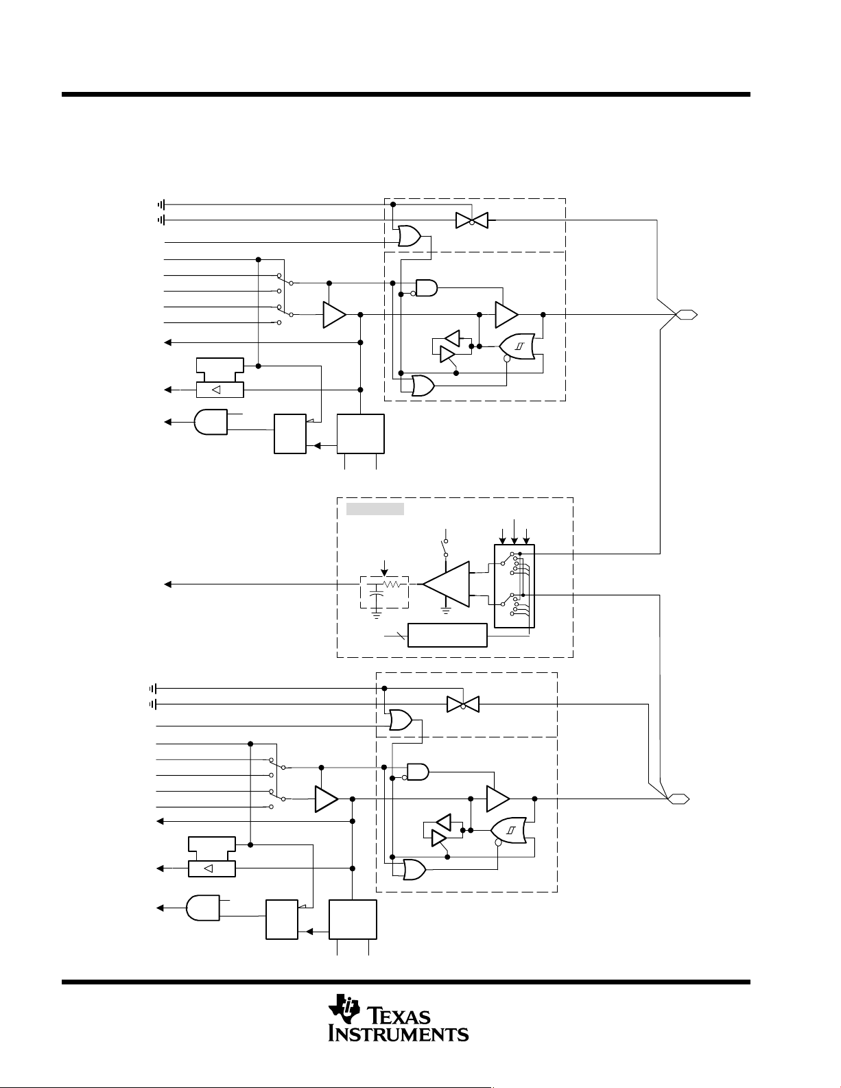
MSP430x43x1, MSP430x43x, MSP430x44x
MIXED SIGNAL MICROCONTROLLER
SLAS344F − JANUARY 2002 − REVISED MAY 2007
APPLICATION INFORMATION
input/output schematic (continued)
Port P1, P1.6, P1.7, input/output with Schmitt-trigger
Pad Logic
CAPD.6
P1SEL.6
P1DIR.6
P1DIR.6
P1OUT.6
DV
P1IN.6
unused
P1IRQ.07
Note: Port function is active if CAPD.6 = 0
SS
EN
D
P1IE.7
P1IFG.7
CCI1B
to Timer_Ax
AVcc
0: Input
1: Output
CAREF
+
−
P2CA
CAEX
CA0
CA1
P1.6/
CA0
0
1
0
1
EN
Q
Set
Interrupt
Edge
Select
P1IES.x P1SEL.x
Comparator_A
CAF
CAREF
Bus
Keeper
2
Reference Block
54
CAPD.7
P1SEL.7
P1DIR.7
P1DIR.7
P1OUT.7
DV
P1IN.7
unused
P1IRQ.07
Note: Port function is active if CAPD.7 = 0
SS
EN
D
P1IE.7
P1IFG.7
0
1
0
1
EN
Q
Set
Interrupt
Edge
Select
P1IES.7 P1SEL.7
POST OFFICE BOX 655303 • DALLAS, TEXAS 75265
Bus
keeper
0: input
1: output
Pad Logic
P1.7/
CA1

MSP430x43x1, MSP430x43x, MSP430x44x
APPLICATION INFORMATION
input/output schematic (continued)
port P2, P2.0, P2.4 to P2.5, input/output with Schmitt-trigger
MIXED SIGNAL MICROCONTROLLER
SLAS344F − JANUARY 2002 − REVISED MAY 2007
DVSS
DVSS
P2SEL.x
P2DIR.x
Direction Control
From Module
P2OUT.x
Module X OUT
P2IN.x
EN
Module X IN
P2IRQ.x EN
x {0,4,5}Note:
PnSel.x PnDIR.x
P2Sel.0 P2DIR.0 P2OUT.0 P2IN.0 P2IE.0 P2IFG.0
P2Sel.4
P2Sel.5
†
Timer_A
‡
USART0
P2DIR.4
P2DIR.5
0
1
0
1
D
P2IE.x
P2IFG.x
Dir. Control
from module
DV
CC
DV
SS
Q
Set
PnOUT.x
P2OUT.4 P2IN.4
P2OUT.5
Interrupt
Edge
Select
P2IES.x P2SEL.x
Module X
OUT
†
Out2 sig. CCI2AP2DIR.0
‡
UTXD0
DV
SS
0: Input
1: Output
Bus
Keeper
PnIN.x PnIE.x PnIFG.x PnIES.xModule X IN
†
unused
‡
P2IN.5
URXD0
Pad Logic
P2IE.4
P2IE.5 P2IFG.5
P2IFG.4 P2IES.4
P2.0/TA2
P2.4/UTXD0
P2.5/URXD0
P2IES.0
P2IES.5
POST OFFICE BOX 655303 • DALLAS, TEXAS 75265
55
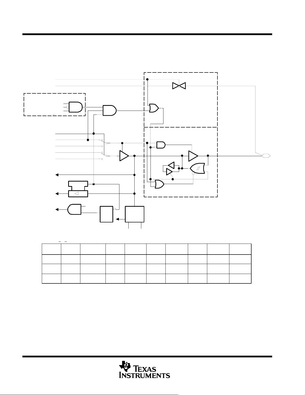
MSP430x43x1, MSP430x43x, MSP430x44x
MIXED SIGNAL MICROCONTROLLER
SLAS344F − JANUARY 2002 − REVISED MAY 2007
APPLICATION INFORMATION
input/output schematic (continued)
port P2, P2.1 to P2.3, input/output with Schmitt-trigger
DVSS
DVSS
Module IN of pin
P1.3/TBOUTH/SVSOUT
Direction Control
From Module
Module X OUT
P1DIR.3
P1SEL.3
P2SEL.x
P2DIR.x
P2OUT.x
P2IN.x
Module X IN
P2IRQ.x
EN
D
P2IE.x
P2IFG.x
Pad Logic
0
1
0
1
EN
Q
Set
Interrupt
Edge
Select
Bus
Keeper
0: Input
1: Output
P2.1/TB0
P2.2/TB1
P2.3/TB2
P2IES.x P2SEL.x
1< x< 3Note:
PnSel.x PnDIR.x
P2Sel.1 P2DIR.1 P2OUT.1 P2IN.1 P2IE.1 P2IFG.1 P2IES.1
P2Sel.2 P2DIR.2 P2OUT.2 P2IN.2 P2IE.2 P2IFG.2 P2IES.2
P2Sel.3 P2DIR.3 P2OUT.3 P2IN.3 P2IE.3 P2IFG.3 P2IES.3
†
Timer_B
Dir. Control
from module
P2DIR.1
P2DIR.2
P2DIR.3 Out2 sig.
PnOUT.x
Module X
OUT
Out0 sig.
Out1 sig.
PnIN.x PnIE.x PnIFG.x PnIES.xModule X IN
†
†
†
CCI0A
CCI0B
CCI1A
CCI1B
CCI2A
CCI2B
†
†
†
56
POST OFFICE BOX 655303 • DALLAS, TEXAS 75265
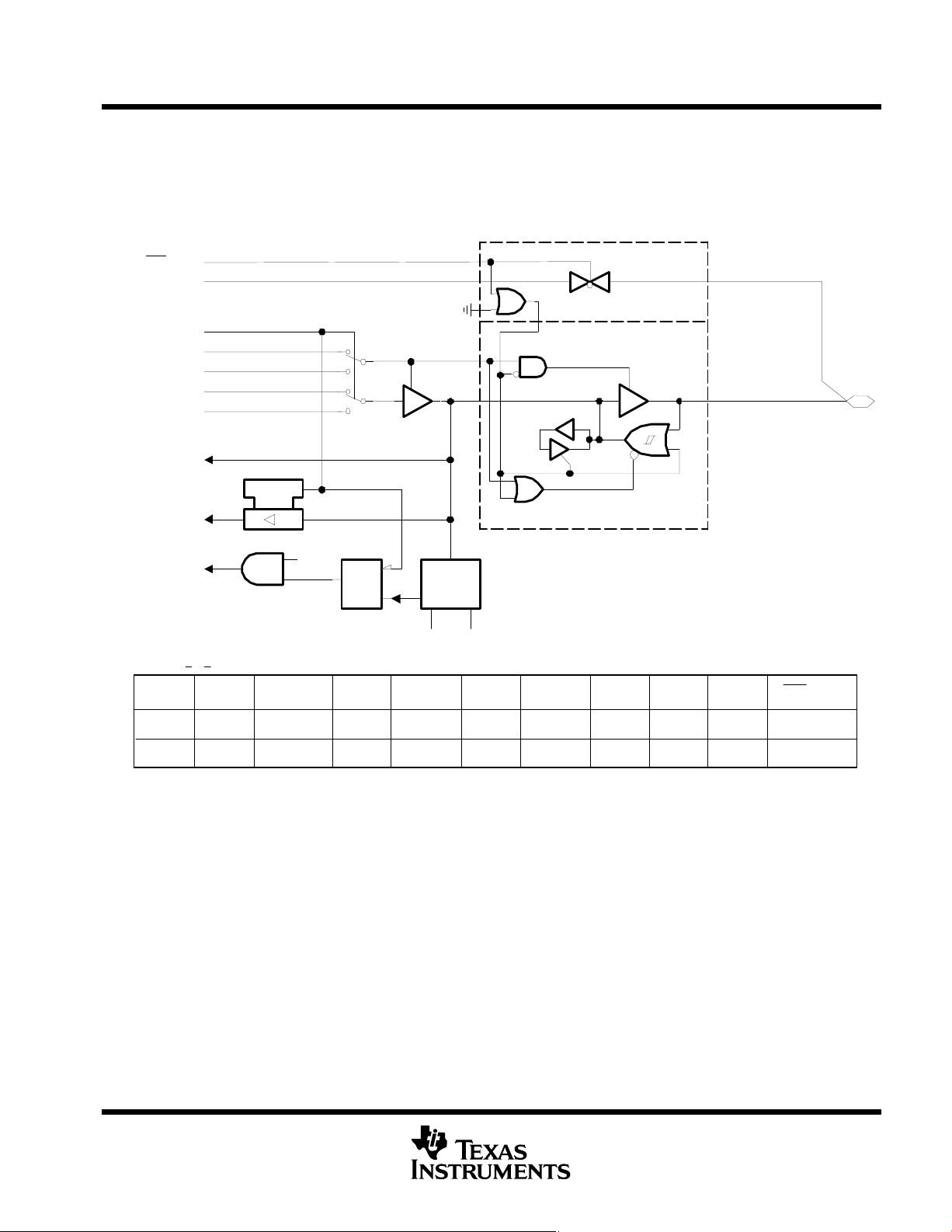
APPLICATION INFORMATION
input/output schematic (continued)
port P2, P2.6 to P2.7, input/output with Schmitt-trigger
0: Port active
1: Segment xx function active
/LCD
Port
Segment xx
‡
‡
MSP430x43x1, MSP430x43x, MSP430x44x
MIXED SIGNAL MICROCONTROLLER
SLAS344F − JANUARY 2002 − REVISED MAY 2007
Pad Logic
P2SEL.x
P2DIR.x
Direction Control
From Module
P2OUT.x
Module X OUT
P2IN.x
EN
Module X IN
P2IRQ.x
6< x< 7Note:
PnSel.x PnDIR.x
P2Sel.6 P2DIR.6
P2Sel.7 P2DIR.7
†
Comparator_A
‡
Port/LCD signal is 1 only with MSP430xIPN and LCDM ≥40h.
§
ADC12
D
P2IFG.x
Dir. Control
from module
P2DIR.6
P2DIR.7
P2IE.x
0
1
0
1
EN
Q
Set
PnOUT.x
P2OUT.6
P2OUT.7
Interrupt
Edge
Select
P2IES.x P2SEL.x
Module X
OUT
CAOUT
ADC12CLK
PnIN.x PnIE.x PnIFG.x PnIES.xModule X IN
†
P2IN.6
§
P2IN.7 unused
Bus
Keeper
unused
0: Input
1: Output
P2IE.6
P2IE.7
P2IFG.6
P2IFG.7
P2.6/CAOUT/S19
P2.7/ADC12CLK/S18
‡
Segment function
only available with
MSP430x43x(1)IPN
Port/LCD
P2IES.6
P2IES.7
0: LCDM<40h
0: LCDM<40h
‡
‡
‡
‡
‡
POST OFFICE BOX 655303 • DALLAS, TEXAS 75265
57

MSP430x43x1, MSP430x43x, MSP430x44x
MIXED SIGNAL MICROCONTROLLER
SLAS344F − JANUARY 2002 − REVISED MAY 2007
APPLICATION INFORMATION
input/output schematic (continued)
port P3, P3.0 to P3.3, input/output with Schmitt-trigger
LCDM.5
LCDM.6
LCDM.7
Segment xx
P3SEL.x
P3DIR.x
Direction Control
From Module
P3OUT.x
Module X OUT
P3IN.x
Module X IN
Note: 0 ≤ x ≤ 3
MSP430x43x(1)IPN (80-Pin) Only
0: Port active
1: Segment xx function active
x43xIPZ and x44xIPZ have no segment
function on Port P3: Both lines are low.
OUT
DV
0: Input
1: Output
PnIN.x Module X IN
SS
0
1
0
1
EN
D
PnSel.x PnDIR.x PnOUT.x
P3Sel.0 P3DIR.0 P3OUT.0 P3IN.0
P3Sel.1 P3DIR.1 P3OUT.1 P3IN.1
P3Sel.2 P3DIR.2 P3OUT.2 P3IN.2
P3Sel.3 P3DIR.3 P3OUT.3 P3IN.3
Direction
Control
From Module
DV
SS
DCM_SIMO0
DCM_SOMI0
DCM_UCLK0
Bus
Keeper
Module X
SIMO0(out)
SOMIO(out)
UCLK0(out)
Pad Logic
STE0(in)
SIMO0(in)
SOMI0(in)
UCLK0(in)
P3.0/STEO/S31
P3.1/SIMO0/S30
P3.2/SOMI0/S29
P3.3/UCLK0/S28
†
†
†
†
†
S24 to S31 shared with port function only at MSP430x43x(1)IPN (80-pin QFP)
Direction Control for SIMO0 and UCLK0
SYNC
MM
STC
DCM_SIMO0
DCM_UCLK0
STE
58
POST OFFICE BOX 655303 • DALLAS, TEXAS 75265
SYNC
MM
STC
STE
Direction Control for SOMI0
DCM_SOMI0

APPLICATION INFORMATION
input/output schematic (continued)
port P3, P3.4 to P3.7, input/output with Schmitt-trigger
0: Port active
†
or DVSS
LCDM.7
Segmentxx† or DVSS
TBOUTHiZ# or DVSS
P3SEL.x
P3DIR.x
Direction Control
From Module
P3OUT.x
Module XOUT
P3IN.x
Module X IN
‡
‡
§
1: Segment xx function active
0
1
0
1
EN
D
MSP430x43x1, MSP430x43x, MSP430x44x
MIXED SIGNAL MICROCONTROLLER
SLAS344F − JANUARY 2002 − REVISED MAY 2007
Pad Logic
0: Input
1: Output
Bus
Keeper
’x43x(1)IPN ’x43xIPZ ’x44x
80-Pin
P3.4/S27
P3.5/S26
P3.6/S25
P3.7/S24
100-Pin
P3.4
P3.5
P3.6
P3.7
P3.4/TB3
P3.5/TB4
P3.6/TB5
P3.7/TB6
4< x< 7Note:
PnSel.x PnDIR.x
P3Sel.4 P3DIR.4 P3OUT.4 P3IN.4
P3Sel.5
P3Sel.6 P3DIR.6
P3Sel.7 P3DIR.7
†
MSP430x43x(1)IPN
‡
MSP430x43xIPZ, MSP430x44xIPZ
§
MSP430x43x(1)
#
MSP430x44x
Module IN of pin
P1.3/TBOUTH/SVSOUT
P3DIR.5 P3OUT.5 P3IN.5
P1DIR.3
P1SEL.3
P3DIR.x
P3SEL.x
Dir. Control
from module
P3DIR.4
P3DIR.5
P3DIR.6
P3DIR.7
PnOUT.x
P3OUT.6
P3OUT.7
Module X
OUT
DVSS
OUT3
DVSS
OUT4
DVSS
OUT5
DVSS
OUT6
TBOUTHiZ
PnIN.x Module X IN
§
#
§
#
§
P3IN.6
#
§
P3IN.7
#
unused
CCI3A/B
unused
CCI4A/B
unused
CCI5A/B
unused
CCI6A
§
#
§
#
§
#
§
#
POST OFFICE BOX 655303 • DALLAS, TEXAS 75265
59

MSP430x43x1, MSP430x43x, MSP430x44x
MIXED SIGNAL MICROCONTROLLER
SLAS344F − JANUARY 2002 − REVISED MAY 2007
APPLICATION INFORMATION
input/output schematic (continued)
port P4, P4.0 to P4.7, input/output with Schmitt-trigger
0: Port active
Port/LCD
Segment xx
§
1: Segment xx function active
Pad Logic
P4SEL.x
P4DIR.x
Direction Control
From Module
P4OUT.x
Module X OUT
P4IN.x
Module X IN
0< x< 7Note:
0
0: Input
1: Output
1
0
1
Bus
Keeper
EN
D
Direction
PnSel.x PnDIR.x PnOUT.x
P4Sel.0 P4DIR.0 P4OUT.0 P4IN.0
P4Sel.1 P4DIR.1 P4OUT.1 P4IN.1
P4Sel.2 P4DIR.2 P4OUT.2 P4IN.2
P4Sel.3 P4DIR.3 P4OUT.3 P4IN.3
P4Sel.4 P4DIR.4 P4OUT.4 P4IN.4
P4Sel.5 P4DIR.5 P4OUT.5 P4IN.5
P4Sel.6 P4DIR.6
Control
From Module
†
P4DIR.0
DV
CC‡
†
P4DIR.1
DV
SS‡
P4DIR.2
DV
SS‡
P4DIR3.
DCM_SIMO1
P4DIR4.
DCM_SOMI
†
P4DIR5.
DCM_UCLK1
P4DIR.6
†
†
‡
†
1‡
‡
P4OUT.6
Module X
OUT
†
DV
SS
‡
UTXD1
DV
SS
DV
SS
†
DV
SS
SIMO1(out)
DV
SS
SOMI1(out)
†
DV
SS
UCLK1(out)
DV
SS
PnIN.x Module X IN
‡
†
‡
‡
P4IN.6
unused
unused†
URXD1
unused†
STE1(in)‡
unused†
SIMO1(in)‡
unused
SOMI1(in)‡
unused†
UCLK1(in)‡
unused
x43x(1)IPN
80-Pin
QFP:
P4.7/S2
P4.6/S3
P4.5/S4
P4.3/S6
P4.4/S5
P4.2/S7
P4.1/S8
P4.0/S9
‡
x43xIPZ
100-Pin
QFP:
P4.7/S34
P4.6/S35
P4.5/S36
P4.3/S37
P4.4/S38
P4.2/S39
P4.0
P4.1
x44x
P4.7/S34
P4.6/S35
P4.5/UCLK1/S36
P4.4/SMO1/S37
P4.3/SIMO1/S38
P4.2/STE1/S39
P4.1/URXD1
P4.0/UTXD1
†
Signal at MSP430x43x(1)
‡
Signal at MSP430x44x
DEVICE
P4Sel.7 P4DIR.7
PORT BITS PORT FUNCTION LCD SEG. FUNCTION
P4DIR.7
P4OUT.7
DV
SS
P4IN.7 unused
x43x(1)IPN 80-pin QFP P4.0 . . .P4.7 LCDM < 020h LCDM ≥ 020h
x43xIPZ 100-pin QFP P4.2 . . .P4.5 LCDM < 0E0h LCDM ≥ 0E0h
x44xIPZ 100-pin QFP P4.6 . . .P4.7 LCDM < 0C0h LCDM ≥ 0C0h
60
POST OFFICE BOX 655303 • DALLAS, TEXAS 75265

MSP430x43x1, MSP430x43x, MSP430x44x
MIXED SIGNAL MICROCONTROLLER
APPLICATION INFORMATION
input/output schematic (continued)
port P4, P4.0 to P4.7, input/output with Schmitt-trigger (continued)
SLAS344F − JANUARY 2002 − REVISED MAY 2007
Direction Control for SIMO1 and UCLK1 Direction Control for SOMI1
SYNC
MM
STC
STE
DCM_SIMO1
DCM_UCLK1
port P5, P5.0 to P5.1, input/output with Schmitt-trigger
0: Port active
Port/LCD
Segment
P5SEL.x
P5DIR.x
Direction Control
From Module
P5OUT.x
Module X OUT
P5IN.x
1: Segment function active
0
1
0
1
SYNC
MM
STC
STE
Bus
Keeper
DCM_SOMI1
Segment Pad Logic
Port Pad Logic
0: Input
1: Output
P5.0/S1
P5.1/S0
EN
Module X IN
0< x< 1Note:
PnSel.x PnDIR.x
P5Sel.0 P5DIR.0 P5OUT.0 P5IN.0
P5Sel.1 P5DIR.1 P5OUT.1 P5IN.1
D
Dir. Control
from module
P5DIR.0
P5DIR.1
PnOUT.x
Module X
OUT
DV
SS
DV
SS
PnIN.x Module X IN
unused
unused
Segment
S1
S0
Port/LCD
0: LCDM<20h
0: LCDM<20h
POST OFFICE BOX 655303 • DALLAS, TEXAS 75265
61

MSP430x43x1, MSP430x43x, MSP430x44x
MIXED SIGNAL MICROCONTROLLER
SLAS344F − JANUARY 2002 − REVISED MAY 2007
APPLICATION INFORMATION
input/output schematic (continued)
port P5, P5.2 to P5.4, input/output with Schmitt-trigger
Port/LCD
LCD signal
P5SEL.x
P5DIR.x
Direction Control
From Module
P5OUT.x
Module X OUT
P5IN.x
Module X IN
0: Port active
1: LCD function active
0
1
0
1
EN
D
2< x< 4Note:
PnSel.x PnDIR.x
P5Sel.2 P5DIR.2 P5OUT.2 P5IN.2
Dir. Control
from module
P5DIR.2
PnOUT.x
Module X
OUT
DV
Bus
Keeper
PnIN.x Module X IN
SS
0: Input
1: Output
unused
Pad Logic
LCD signal
COM1
P5.2/COM1
P5.3/COM2
P5.4/COM3
Port/LCD
P5SEL.2
P5Sel.3 P5DIR.3 P5OUT.3 P5IN.3
P5Sel.4 P5DIR.4 P5OUT.4 P5IN.4
P5DIR.3
P5DIR.4
DV
DV
SS
SS
unused
unused
COM2
COM3
P5SEL.3
P5SEL.4
62
POST OFFICE BOX 655303 • DALLAS, TEXAS 75265

APPLICATION INFORMATION
input/output schematic (continued)
port P5, P5.5 to P5.7, input/output with Schmitt-trigger
MSP430x43x1, MSP430x43x, MSP430x44x
MIXED SIGNAL MICROCONTROLLER
SLAS344F − JANUARY 2002 − REVISED MAY 2007
Port/LCD
LCD signal
P5SEL.x
P5DIR.x
Direction Control
From Module
P5OUT.x
Module X OUT
P5IN.x
Module X IN
0: Port active
1: LCD function active
0
1
0
1
EN
D
5< x< 7Note:
PnSel.x PnDIR.x
P5Sel.5 P5DIR.5 P5OUT.5 P5IN.5
Dir. Control
from module
P5DIR.5
PnOUT.x
Module X
OUT
DV
Bus
Keeper
PnIN.x Module X IN
SS
0: Input
1: Output
unused
Pad Logic
LCD signal
P5.5/R13
P5.6/R23
P5.7/R33
Port/LCD
R13 P5SEL.5
P5Sel.6 P5DIR.6 P5OUT.6 P5IN.6
P5Sel.7 P5DIR.7 P5OUT.7 P5IN.7
P5DIR.6
P5DIR.7
DV
DV
SS
SS
unused
unused
R23
R33
P5SEL.6
P5SEL.7
POST OFFICE BOX 655303 • DALLAS, TEXAS 75265
63
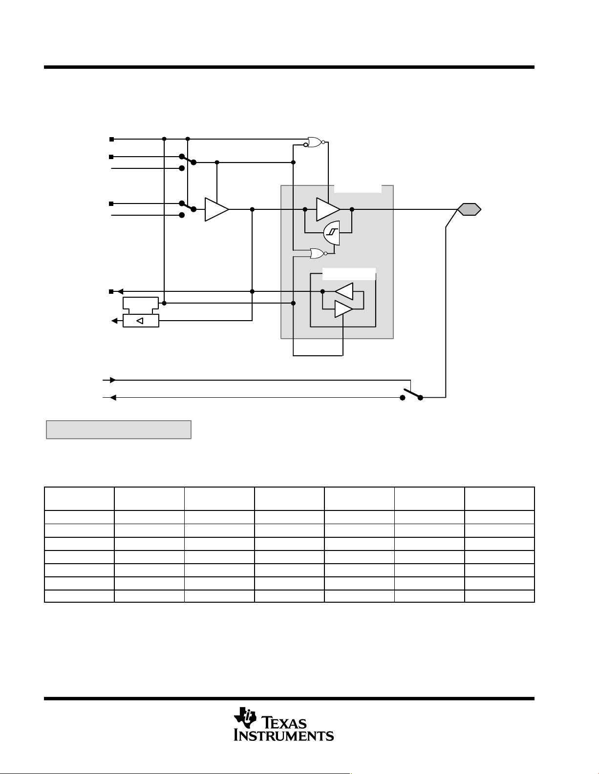
MSP430x43x1, MSP430x43x, MSP430x44x
MIXED SIGNAL MICROCONTROLLER
SLAS344F − JANUARY 2002 − REVISED MAY 2007
APPLICATION INFORMATION
input/output schematic (continued)
port P6, P6.0 to P6.6, input/output with Schmitt-trigger
P6SEL.x
P6DIR.x
Direction Control
From Module
P6OUT.x
Module X OUT
P6IN.x
0
1
0
1
EN
0: Input
1: Output
Pad Logic
Bus Keeper
P6.0/A0 ..
P6.6/A6
Module X IN
From ADC
To ADC
x: Bit Identifier, 0 to 6 for Port P6
NOTE: Analog signals applied to digital gates can cause current flow from the positive to the negative terminal. The throughput current flows if
the analog signal is in the range of transitions 0→1 or 1→0. The value of the throughput current depends on the driving capability of the
gate. For MSP430, it is approximately 100 μA.
Use P6SEL.x=1 to prevent throughput current. P6SEL.x should be set, even if the signal at the pin is not being used by the ADC12.
PnSel.x
P6Sel.0 P6DIR.0 P6DIR.0 P6OUT.0 DV
P6Sel.1 P6DIR.1 P6DIR.1 P6OUT.1 DV
P6Sel.2 P6DIR.2 P6DIR.2 P6OUT.2 DV
P6Sel.3 P6DIR.3 P6DIR.3 P6OUT.3 DV
P6Sel.4 P6DIR.4 P6DIR.4 P6OUT.4 DV
P6Sel.5 P6DIR.5 P6DIR.5 P6OUT.5 DV
P6Sel.6 P6DIR.6 P6DIR.6 P6OUT.6 DV
NOTE: The signal at pins P6.x/Ax is used by the 12-bit ADC module.
D
PnDIR.x
Dir. Control
From Module
PnOUT.x Module X OUT PnIN.x Module X IN
SS
SS
SS
SS
SS
SS
SS
P6IN.0 unused
P6IN.1 unused
P6IN.2 unused
P6IN.3 unused
P6IN.4 unused
P6IN.5 unused
P6IN.6 unused
64
POST OFFICE BOX 655303 • DALLAS, TEXAS 75265

APPLICATION INFORMATION
input/output schematic (continued)
port P6, P6.7, input/output with Schmitt-trigger
P6SEL.x
VLP(SVS)=15
MSP430x43x1, MSP430x43x, MSP430x44x
MIXED SIGNAL MICROCONTROLLER
SLAS344F − JANUARY 2002 − REVISED MAY 2007
P6DIR.x
Direction Control
From Module
P6OUT.x
Module X OUT
P6IN.x
EN
Module X IN
Note: Not implemented in the MSP430x43x1 devices
From ADC
To ADC
To Brownout/SVS Module
x: Bit Identifier, 7 for Port P6
NOTE: Analog signals applied to digital gates can cause current flow from the positive to the negative terminal. The throughput current flows if
the analog signal is in the range of transitions 0→1 or 1→0. The value of the throughput current depends on the driving capability of the
gate. For MSP430, it is approximately 100 μA.
Use P6SEL.x=1 to prevent throughput current. P6SEL.x should be set, even if the signal at the pin is not being used by the ADC12.
0
1
0
1
D
0: Input
1: Output
Pad Logic
P6.7/A7/SVSIN
Bus Keeper
PnSel.x
P6Sel.7 P6DIR.7 P6DIR.7 P6OUT.7 DV
NOTE: The signal at pins P6.x/Ax is used by the 12-bit ADC module.
The signal at pin P6.7/A7/SVSIN is also connected to the input multiplexer in the module brownout/supply voltage supervisor.
PnDIR.x
Dir. Control
From Module
POST OFFICE BOX 655303 • DALLAS, TEXAS 75265
PnOUT.x Module X OUT PnIN.x Module X IN
SS
P6IN.7 unused
65
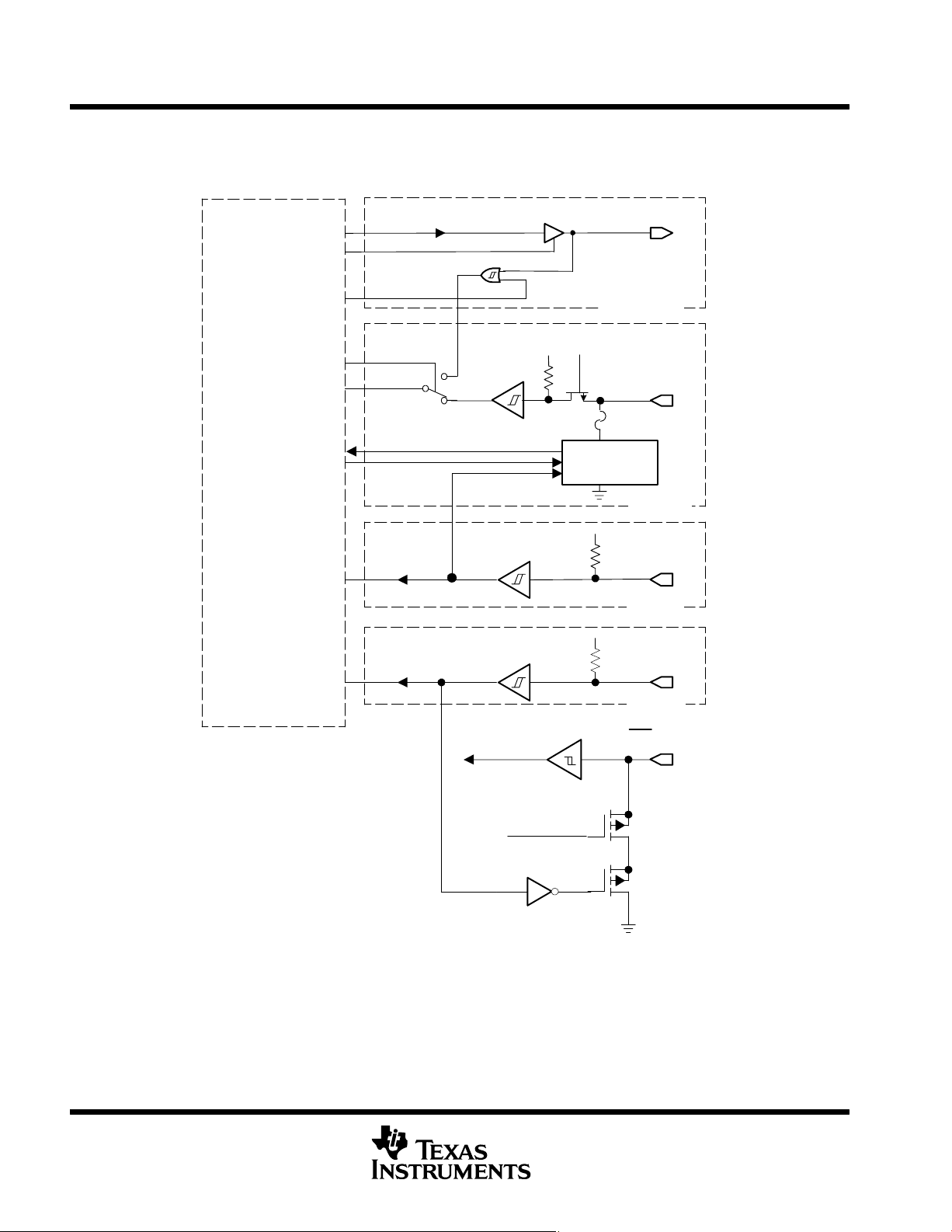
MSP430x43x1, MSP430x43x, MSP430x44x
MIXED SIGNAL MICROCONTROLLER
SLAS344F − JANUARY 2002 − REVISED MAY 2007
APPLICATION INFORMATION
JTAG pins TMS, TCK, TDI/TCLK, TDO/TDI, input/output with Schmitt-trigger or output
TDO
Controlled by JTAG
Controlled by JTAG
JTAG
Controlled
by JTAG
TDI
DV
CC
Burn and Test
TDO/TDI
Fuse
Test
and
Emulation
Module
TMS
TCK
TCK
Tau ~ 50 ns
Brownout
TDI/TCLK
DV
CC
TMS
DV
CC
TCK
RST/NMI
D
G
G
U
S
D
U
S
66
POST OFFICE BOX 655303 • DALLAS, TEXAS 75265
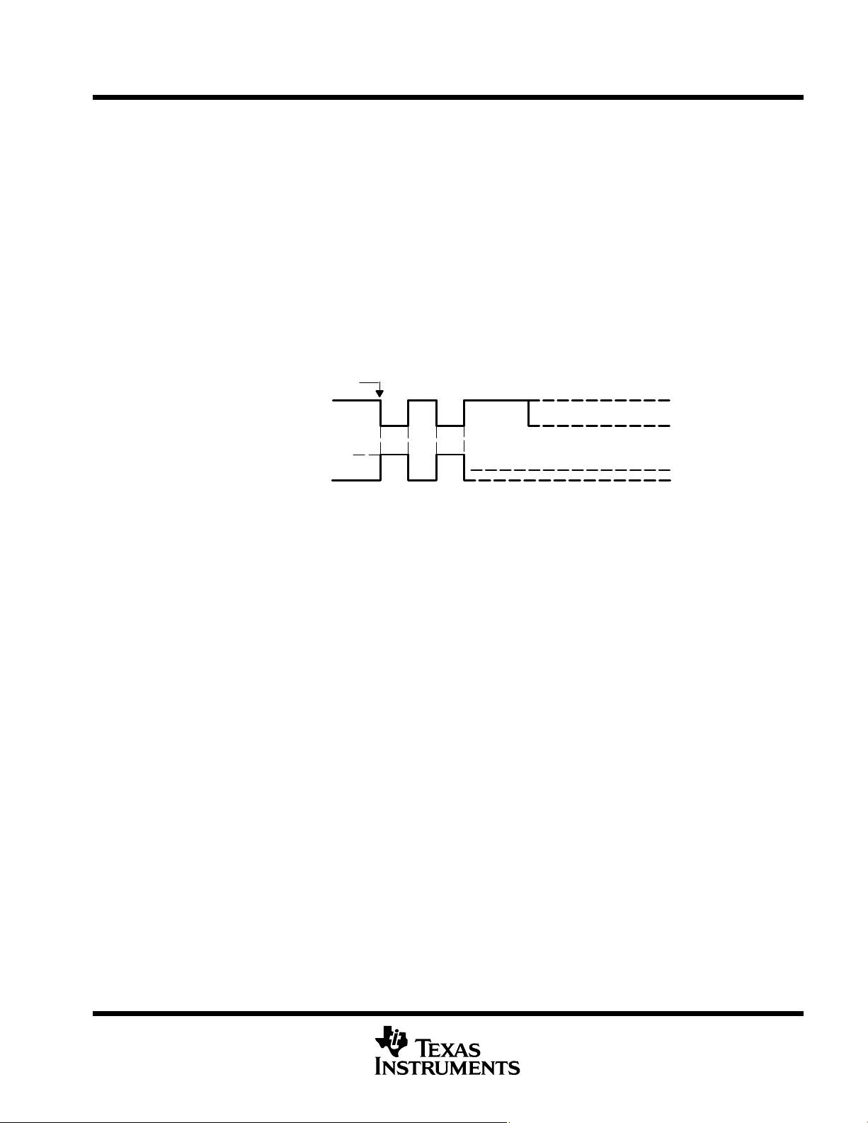
MSP430x43x1, MSP430x43x, MSP430x44x
MIXED SIGNAL MICROCONTROLLER
SLAS344F − JANUARY 2002 − REVISED MAY 2007
APPLICATION INFORMATION
JTAG fuse check mode
MSP430 devices that have the fuse on the TDI/TCLK terminal have a fuse check mode that tests the continuity
of the fuse the first time the JTAG port is accessed after a power-on reset (POR). When activated, a fuse check
current (I
taken to avoid accidentally activating the fuse check mode and increasing overall system power consumption.
Activation of the fuse check mode occurs with the first negative edge on the TMS pin after power up or if the
TMS is being held low during power up. The second positive edge on the TMS pin deactivates the fuse check
mode. After deactivation, the fuse check mode remains inactive until another POR occurs. After each POR the
fuse check mode has the potential to be activated.
The fuse check current only flows when the fuse check mode is active and the TMS pin is in a low state (see
Figure 21). Therefore, the additional current flow can be prevented by holding the TMS pin high (default
condition). The JTAG pins are terminated internally and therefore do not require external termination.
) of 1 mA at 3 V can flow from the TDI/TCLK pin to ground if the fuse is not burned. Care must be
(TF)
Time TMS Goes Low After POR
TMS
I
I
TDI/TCLK
(TF)
Figure 21. Fuse Check Mode Current MSP430x43x(1), MSP430x44x
POST OFFICE BOX 655303 • DALLAS, TEXAS 75265
67
MSP430x43x1, MSP430x43x, MSP430x44x
MIXED SIGNAL MICROCONTROLLER
SLAS344F − JANUARY 2002 − REVISED MAY 2007
Data Sheet Revision History
Literature
Number
Added MSP430F43x1 devices
Updated functional block diagram (page 6)
Clarified test conditions in recommended operating conditions table (page 27)
SLAS344E
SLAS344F Added MSP430F43x1 devices in PZ (100 pin) package
NOTE: Page and figure numbers refer to the respective document revision.
Clarified test conditions in electrical characteristics table (page 28)
Added Port 2 through Port 5 to leakage current table (page 29)
Corrected y-axis unit on Figures 6 and 7; changed from V to mV (page 34)
Clarified test conditions in USART0/USART1 table (page 40)
Changed t
maximum value from 4 ms to 10 ms in Flash memory table (page 46)
CPT
Summary
68
POST OFFICE BOX 655303 • DALLAS, TEXAS 75265
PACKAGE OPTION ADDENDUM
www.ti.com
PACKAGING INFORMATION
Orderable Device Status
MSP430F4351IPN ACTIVE LQFP PN 80 50 Green (RoHS &
MSP430F4351IPNR ACTIVE LQFP PN 80 1000 Green (RoHS &
MSP430F4351IPZ ACTIVE LQFP PZ 100 90 Green (RoHS &
MSP430F4351IPZR ACTIVE LQFP PZ 100 1000 Green (RoHS &
MSP430F435IPN ACTIVE LQFP PN 80 119 Green (RoHS &
MSP430F435IPNR ACTIVE LQFP PN 80 1000 Green (RoHS &
MSP430F435IPZ ACTIVE LQFP PZ 100 90 Green (RoHS&
MSP430F435IPZR ACTIVE LQFP PZ 100 1000 Green (RoHS &
MSP430F4361IPN ACTIVE LQFP PN 80 50 Green (RoHS &
MSP430F4361IPNR ACTIVE LQFP PN 80 1000 Green (RoHS &
MSP430F4361IPZ ACTIVE LQFP PZ 100 90 Green (RoHS &
MSP430F4361IPZR ACTIVE LQFP PZ 100 1000 Green (RoHS &
MSP430F436IPN ACTIVE LQFP PN 80 119 Green (RoHS &
MSP430F436IPNR ACTIVE LQFP PN 80 1000 Green (RoHS &
MSP430F436IPZ ACTIVE LQFP PZ 100 90 Green (RoHS&
MSP430F436IPZR ACTIVE LQFP PZ 100 1000 Green (RoHS &
MSP430F4371IPN ACTIVE LQFP PN 80 50 Green (RoHS &
MSP430F4371IPNR ACTIVE LQFP PN 80 1000 Green (RoHS &
MSP430F4371IPZ PREVIEW LQFP PZ 100 90 TBD Call TI Call TI
MSP430F4371IPZR ACTIVE LQFP PZ 100 1000 Green (RoHS &
MSP430F437IPN ACTIVE LQFP PN 80 119 Green (RoHS &
MSP430F437IPNR ACTIVE LQFP PN 80 1000 Green (RoHS &
MSP430F437IPZ ACTIVE LQFP PZ 100 90 Green (RoHS&
MSP430F437IPZR ACTIVE LQFP PZ 100 1000 Green (RoHS &
MSP430F447IPZ ACTIVE LQFP PZ 100 90 Green (RoHS&
(1)
Package
Type
Package
Drawing
Pins Package
Qty
Eco Plan
no Sb/Br)
no Sb/Br)
no Sb/Br)
no Sb/Br)
no Sb/Br)
no Sb/Br)
no Sb/Br)
no Sb/Br)
no Sb/Br)
no Sb/Br)
no Sb/Br)
no Sb/Br)
no Sb/Br)
no Sb/Br)
no Sb/Br)
no Sb/Br)
no Sb/Br)
no Sb/Br)
no Sb/Br)
no Sb/Br)
no Sb/Br)
no Sb/Br)
no Sb/Br)
no Sb/Br)
(2)
Lead/Ball Finish MSL Peak Temp
CU NIPDAU Level-3-260C-168 HR
CU NIPDAU Level-3-260C-168 HR
CU NIPDAU Level-3-260C-168 HR
CU NIPDAU Level-3-260C-168 HR
CU NIPDAU Level-3-260C-168 HR
CU NIPDAU Level-3-260C-168 HR
CU NIPDAU Level-3-260C-168 HR
CU NIPDAU Level-3-260C-168 HR
CU NIPDAU Level-3-260C-168 HR
CU NIPDAU Level-3-260C-168 HR
CU NIPDAU Level-3-260C-168 HR
CU NIPDAU Level-3-260C-168 HR
CU NIPDAU Level-3-260C-168 HR
CU NIPDAU Level-3-260C-168 HR
CU NIPDAU Level-3-260C-168 HR
CU NIPDAU Level-3-260C-168 HR
CU NIPDAU Level-3-260C-168 HR
CU NIPDAU Level-3-260C-168 HR
CU NIPDAU Level-3-260C-168 HR
CU NIPDAU Level-3-260C-168 HR
CU NIPDAU Level-3-260C-168 HR
CU NIPDAU Level-3-260C-168 HR
CU NIPDAU Level-3-260C-168 HR
CU NIPDAU Level-3-260C-168 HR
25-Sep-2007
(3)
Addendum-Page 1
PACKAGE OPTION ADDENDUM
www.ti.com
Orderable Device Status
(1)
Package
Type
Package
Drawing
Pins Package
Qty
Eco Plan
(2)
MSP430F447IPZR ACTIVE LQFP PZ 100 1000 Green (RoHS &
Lead/Ball Finish MSL Peak Temp
CU NIPDAU Level-3-260C-168 HR
25-Sep-2007
(3)
no Sb/Br)
MSP430F448IPZ ACTIVE LQFP PZ 100 90 Green (RoHS&
CU NIPDAU Level-3-260C-168 HR
no Sb/Br)
MSP430F448IPZR ACTIVE LQFP PZ 100 1000 Green (RoHS &
CU NIPDAU Level-3-260C-168 HR
no Sb/Br)
MSP430F449IPZ ACTIVE LQFP PZ 100 90 Green (RoHS&
CU NIPDAU Level-3-260C-168 HR
no Sb/Br)
MSP430F449IPZR ACTIVE LQFP PZ 100 1000 Green (RoHS &
CU NIPDAU Level-3-260C-168 HR
no Sb/Br)
(1)
The marketing status valuesare defined as follows:
ACTIVE: Product device recommendedfor new designs.
LIFEBUY: TI has announcedthat the device will be discontinued,and a lifetime-buy period is ineffect.
NRND: Not recommended for new designs. Device is in production to support existing customers, but TI does not recommend using this part in
a new design.
PREVIEW: Device has beenannounced but is not in production.Samples may or may not beavailable.
OBSOLETE: TI has discontinuedthe production of the device.
(2)
Eco Plan - The planned eco-friendly classification: Pb-Free (RoHS), Pb-Free (RoHS Exempt), or Green (RoHS & no Sb/Br) - please check
http://www.ti.com/productcontent for the latestavailability information and additional product contentdetails.
TBD: The Pb-Free/Green conversionplan has not been defined.
Pb-Free (RoHS): TI's terms "Lead-Free" or "Pb-Free" mean semiconductor products that are compatible with the current RoHS requirements
for all 6 substances, including the requirement that lead not exceed 0.1% by weight in homogeneous materials. Where designed to be soldered
at high temperatures, TIPb-Free products are suitable for usein specified lead-free processes.
Pb-Free (RoHS Exempt): This component has a RoHS exemption for either 1) lead-based flip-chip solder bumps used between the die and
package, or 2) lead-based die adhesive used between the die and leadframe. The component is otherwise considered Pb-Free (RoHS
compatible) as defined above.
Green (RoHS & no Sb/Br): TI defines "Green" to mean Pb-Free (RoHS compatible), and free of Bromine (Br) and Antimony (Sb) based flame
retardants (Br or Sbdo not exceed 0.1% by weightin homogeneous material)
(3)
MSL, Peak Temp. -- The Moisture Sensitivity Level rating according to the JEDEC industry standard classifications, and peak solder
temperature.
Important Information and Disclaimer:The information provided on this page represents TI's knowledge and belief as of the date that it is
provided. TI bases its knowledge and belief on information provided by third parties, and makes no representation or warranty as to the
accuracy of such information. Efforts are underway to better integrate information from third parties. TI has taken and continues to take
reasonable steps to provide representative and accurate information but may not have conducted destructive testing or chemical analysis on
incoming materials and chemicals. TI and TI suppliers consider certain information to be proprietary, and thus CAS numbers and other limited
information may not beavailable for release.
In no event shall TI's liability arising out of such information exceed the total purchase price of the TI part(s) at issue in this document sold by TI
to Customer on an annual basis.
Addendum-Page 2
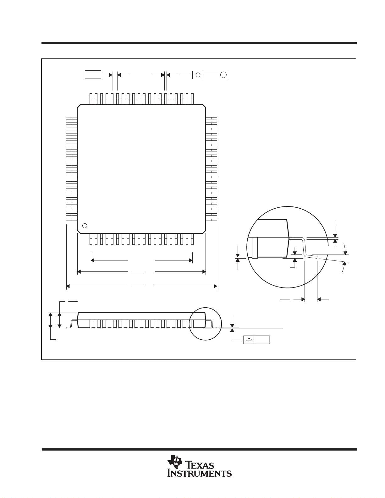
MECHANICAL DATA
MTQF010A – JANUARY 1995 – REVISED DECEMBER 1996
PN (S-PQFP-G80) PLASTIC QUAD FLATPACK
80
61
1,45
1,35
0,50
60
1
9,50 TYP
12,20
SQ
11,80
14,20
SQ
13,80
0,27
0,17
20
41
0,08
M
40
21
0,05 MIN
0,13 NOM
Gage Plane
0,25
0°–7°
0,75
0,45
1,60 MAX
NOTES: A. All linear dimensions are in millimeters.
B. This drawing is subject to change without notice.
C. Falls within JEDEC MS-026
POST OFFICE BOX 655303 • DALLAS, TEXAS 75265
Seating Plane
0,08
4040135 /B 11/96
1
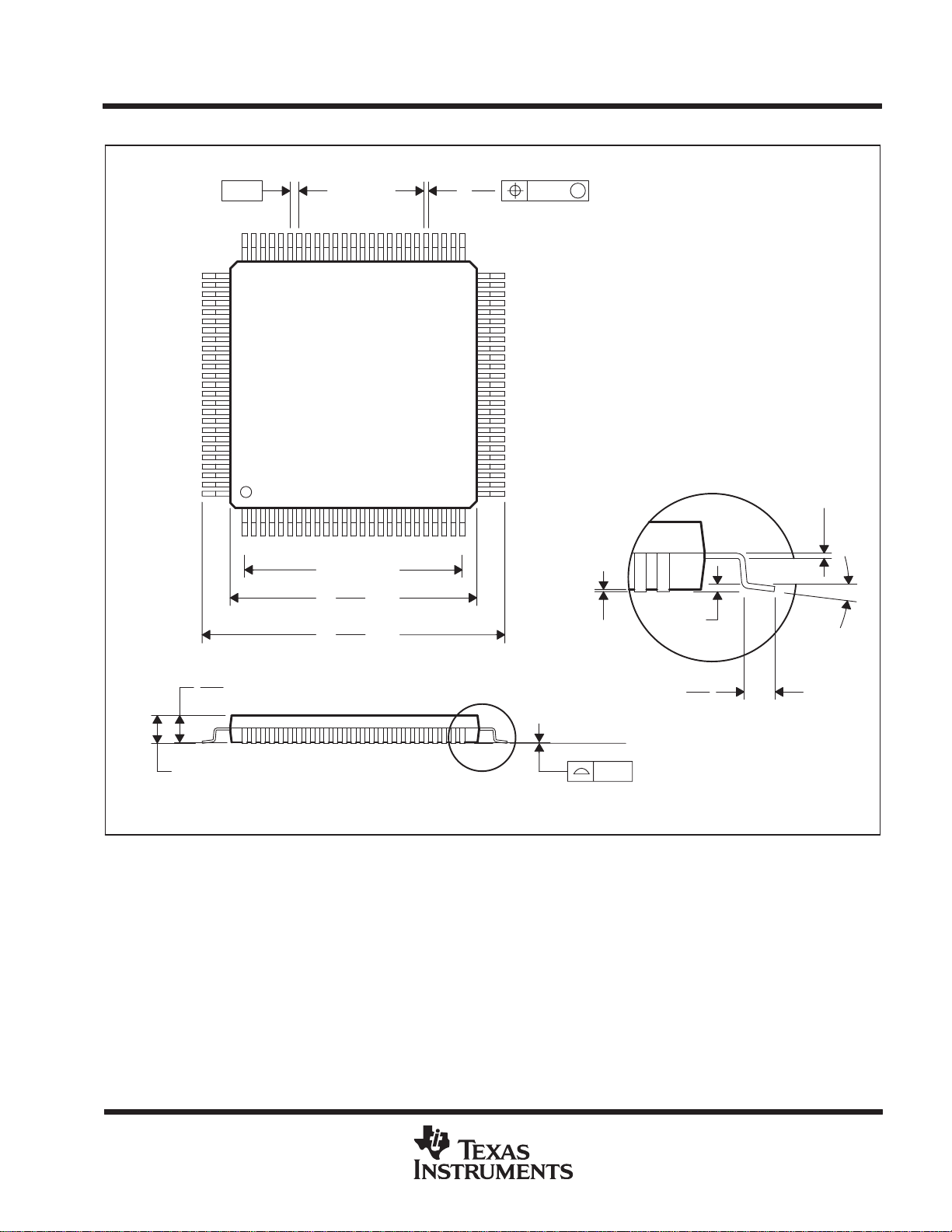
MECHANICAL DATA
MTQF013A – OCTOBER 1994 – REVISED DECEMBER 1996
PZ (S-PQFP-G100) PLASTIC QUAD FLATPACK
76
100
0,50
75
1
12,00 TYP
14,20
SQ
13,80
16,20
SQ
15,80
51
25
0,27
0,17
50
26
0,08
M
0,05 MIN
0,13 NOM
Gage Plane
0,25
0°–7°
1,45
1,35
1,60 MAX
NOTES: A. All linear dimensions are in millimeters.
B. This drawing is subject to change without notice.
C. Falls within JEDEC MS-026
0,75
0,45
Seating Plane
0,08
4040149/B 1 1/96
POST OFFICE BOX 655303 • DALLAS, TEXAS 75265
1

IMPORTANT NOTICE
Texas Instruments Incorporated and its subsidiaries (TI) reserve the right to make corrections, modifications, enhancements,
improvements, and other changes to its products and services at any time and to discontinue any product or service without notice.
Customers should obtain the latest relevant information before placing orders and should verify that such information is current and
complete. All products are sold subject to TI’s terms and conditions of sale supplied at the time of order acknowledgment.
TI warrants performance of its hardware products to the specifications applicable at the time of sale in accordance with TI’s
standard warranty. Testing and other quality control techniques are used to the extent TI deems necessary to support this
warranty. Except where mandated by government requirements, testing of all parameters of each product is not necessarily
performed.
TI assumes no liability for applications assistance or customer product design. Customers are responsible for their products and
applications using TI components. To minimize the risks associated with customer products and applications, customers should
provide adequate design and operating safeguards.
TI does not warrant or represent that any license, either express or implied, is granted under any TI patent right, copyright, mask
work right, or other TI intellectual property right relating to any combination, machine, or process in which TI products or services
are used. Information published by TI regarding third-party products or services does not constitute a license from TI to use such
products or services or a warranty or endorsement thereof. Use of such information may require a license from a third party under
the patents or other intellectual property of the third party, or a license from TI under the patents or other intellectual property of TI.
Reproduction of TI information in TI data books or data sheets is permissible only if reproduction is without alteration and is
accompanied by all associated warranties, conditions, limitations, and notices. Reproduction of this information with alteration is an
unfair and deceptive business practice. TI is not responsible or liable for such altered documentation. Information of third parties
may be subject to additional restrictions.
Resale of TI products or services with statements different from or beyond the parameters stated by TI for that product or service
voids all express and any implied warranties for the associated TI product or service and is an unfair and deceptive business
practice. TI is not responsible or liable for any such statements.
TI products are not authorized for use in safety-critical applications (such as life support) where a failure of the TI product would
reasonably be expected to cause severe personal injury or death, unless officers of the parties have executed an agreement
specifically governing such use. Buyers represent that they have all necessary expertise in the safety and regulatory ramifications
of their applications, and acknowledge and agree that they are solely responsible for all legal, regulatory and safety-related
requirements concerning their products and any use of TI products in such safety-critical applications, notwithstanding any
applications-related information or support that may be provided by TI. Further, Buyers must fully indemnify TI and its
representatives against any damages arising out of the use of TI products in such safety-critical applications.
TI products are neither designed nor intended for use in military/aerospace applications or environments unless the TI products are
specifically designated by TI as military-grade or "enhanced plastic." Only products designated by TI as military-grade meet military
specifications. Buyers acknowledge and agree that any such use of TI products which TI has not designated as military-grade is
solely at the Buyer's risk, and that they are solely responsible for compliance with all legal and regulatory requirements in
connection with such use.
TI products are neither designed nor intended for use in automotive applications or environments unless the specific TI products
are designated by TI as compliant with ISO/TS 16949 requirements. Buyers acknowledge and agree that, if they use any
non-designated products in automotive applications, TI will not be responsible for any failure to meet such requirements.
Following are URLs where you can obtain information on other Texas Instruments products and application solutions:
Products Applications
Amplifiers amplifier.ti.com Audio www.ti.com/audio
Data Converters dataconverter.ti.com Automotive www.ti.com/automotive
DSP dsp.ti.com Broadband www.ti.com/broadband
Interface interface.ti.com Digital Control www.ti.com/digitalcontrol
Logic logic.ti.com Military www.ti.com/military
Power Mgmt power.ti.com Optical Networking www.ti.com/opticalnetwork
Microcontrollers microcontroller.ti.com Security www.ti.com/security
RFID www.ti-rfid.com Telephony www.ti.com/telephony
Low Power www.ti.com/lpw Video & Imaging www.ti.com/video
Wireless
Wireless www.ti.com/wireless
Mailing Address: Texas Instruments, Post Office Box 655303, Dallas, Texas 75265
Copyright © 2007, Texas Instruments Incorporated
 Loading...