

Page 1
查询DRV593供应商
www.ti.com
SLOS401A - SEPTEMBER 2002 REVISED - OCTOBER 2002
±3−A HIGH−EFFICIENCY PWM POWER DRIVER
DRV593
DRV594
FEATURES
D Operation Reduces Output Filter Size and
Cost by 50% Compared to DRV591
D ±3-A Maximum Output Current
D Low Supply Voltage Operation: 2.8 V to 5.5 V
D High Efficiency Generates Less Heat
D Overcurrent and Thermal Protection
D Fault Indicators for Overcurrent, Thermal and
Undervoltage Conditions
D Two Selectable Switching Frequencies
D Internal or External Clock Sync
D PWM Scheme Optimized for EMI
D 9×9 mm PowerPAD Quad Flatpack Package
APPLICATIONS
D Thermoelectric Cooler (TEC) Driver
D Laser Diode Biasing
DESCRIPTION
The DRV593 and DRV594 are high-efficiency,
high-current power amplifiers ideal for driving a wide
variety of thermoelectric cooler elements in systems
powered from 2.8 V to 5.5 V. The operation of the device
requires only one inductor and capacitor for the output
filter, saving significant printed-circuit board area.
Pulse-width modulation (PWM) operation and low output
stage on-resistance significantly decrease power
dissipation in the amplifier.
The DRV593 and DRV594 are internally protected against
thermal and current overloads. Logic-level fault indicators
signal when the junction temperature has reached
approximately 115°C to allow for system-level shutdown
before the amplifier’s internal thermal shutdown circuitry
activates. The fault indicators also signal when an
overcurrent event has occurred. If the overcurrent circuitry
is tripped, the devices automatically reset (see application
information section for more details).
The PWM switching frequency may be set to 500 kHz or
100 kHz depending on system requirements. To eliminate
external components, the gain is fixed at 2.3 V/V for the
DRV593. For the DRV594, the gain is fixed at 14.5 V/V.
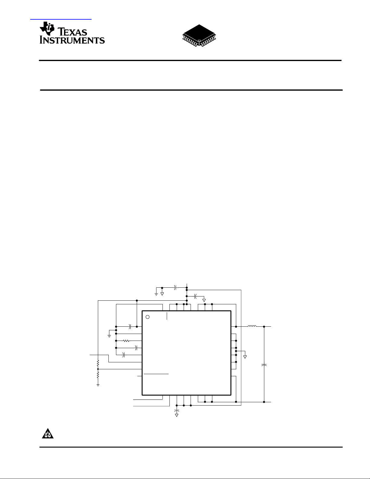
V
DD
1 µF
120 kΩ
DC Control
Voltage
1 kΩ
1 kΩ
Shutdown Control
Please be aware that an important notice concerning availability, standard warranty, and use in critical applications of TexasInstruments
semiconductor products and disclaimers thereto appears at the end of this data sheet.
PowerPAD is a trademark of Texas Instruments.
PRODUCTION DATA information is current as of publication date. Products
conform to specifications per the terms of Texas Instruments standard warranty.
Production processing does not necessarily include testing of all parameters.
220 pF
1 µF
FAULT1
FAULT0
AVDD
AGND (Connect to PowerPAD)
ROSC
COSC
AREF
IN+
IN-INSHUTDOWN
10 µF
FREQ
FAULT1
PVDD
INT/EXT
DRV593
DRV594
FAULT0
PVDD
1 µF
PVDD
PVDD
1 µF
PWM
PVDD
PVDD
H/C
PWM
H/C
PWM
PGND
PGND
PGND
PGND
PGND
PGND
H/C
PWM
H/C
10 µH
Copyright 2002, Texas Instruments Incorporated
To TEC or Laser
Diode Anode
10 µF
To TEC or Laser
Diode Cathode
Page 2
DRV593
DRV594
SLOS401A - SEPTEMBER 2002 REVISED - OCTOBER 2002
www.ti.com
This integrated circuit can be damaged by ESD. Texas
Instruments recommends that all integrated circuits be
handled with appropriate precautions. Failure to observe
proper handling and installation procedures can cause damage.
ESD damage can range from subtle performance degradation to
complete device failure. Precision integrated circuits may be more
susceptible t o damage because very small parametric changes could
cause the device not to meet its published specifications.
ORDERING INFORMATION
T
A
-40°C to 85°C
(1)
This package is available taped and reeled. To order this
packaging option, add an R suffix to the part number (e.g.,
PowerPAD QUAD FLATPACK
(VFP)
DRV593VFP
DRV594VFP
(1)
(1)
DRV593VFPR or DRV594VFPR).
ABSOLUTE MAXIMUM RATINGS
over operating free-air temperature range unless otherwise noted
Supply voltage, AVDD, PVDD -0.3 V to 5.5 V
Input voltage, V
I
Output current, IO (FAULT0, FAULT1) 1 mA
Continuous total power dissipation See Dissipation Rating Table
Operating free-air temperature range, T
Operating junction temperature range, T
Storage temperature range, T
(1)
Stresses beyond those listed under “absolute maximum ratings” may cause permanent damage to the device. These are stress ratings only , and
stg
A
J
functional operation of the device at these or any other conditions beyond those indicated under “recommended operating conditions” is not
implied. Exposure to absolute-maximum-rated conditions for extended periods may affect device reliability .
(1)
DRV593, DRV594
-0.3 V to VDD + 0.3 V
-40°C to 85°C
-40°C to 150°C
-65°C to 165°C
RECOMMENDED OPERATING CONDITIONS
MIN MAX UNIT
Supply voltage, AVDD
High-level input voltage, V
Low-level input voltage, V
Operating free-air temperature, T
PVDD
,
2.8
5.5
IH
IL
A
FREQ, INT/EXT, SHUTDOWN, COSC
FREQ, INT/EXT, SHUTDOWN, COSC
-40
2
0.8
85
V
V
V
°C
PACKAGE DISSIPATION RATINGS
PACKAGE
Θ
JA
(°C/W)
Θ
JC
(°C/W)
(1)
VFP 29.4 1.2 4.1 W
(1)
This data was taken using 2 oz trace and copper pad that is
soldered directly to a JEDEC standard 4-layer 3 in× 3 in PCB.
2
T
A
POWER RATING
= 25°C
Page 3
DRV593
VDD = 5 V, IO = 4 A
VDD = 3.3 V, IO = 4 A
www.ti.com
SLOS401A - SEPTEMBER 2002 REVISED - OCTOBER 2002
ELECTRICAL CHARACTERISTICS
over operating free-air temperature range unless otherwise noted
PARAMETER TEST CONDITIONS MIN TYP MAX UNIT
|VOO| Output offset voltage (measured differentially) VI = VDD/2, IO = 0 A 14 100 mV
|IIH| High-level input current VDD = 5.5V , VI = V
|IIL| Low-level input current VDD = 5.5V , VI = 0 V 1 µA
V
n
V
ICM
A
v
Integrated output noise voltage f = <1 Hz to 10 kHz 40 µV
Common-mode voltage range
Closed-loop voltage gain
VDD = 5 V 1.2 3.8
VDD = 3.3 V 1.2 2.1
DRV593 2.1 2.3 2.6 V/V
DRV594 13.7 14.5 15.3 V/V
Full power bandwidth 60 kHz
V
O
Voltage output (measured dif ferentially)
IO = ±1 A, r
IO = ±3 A, r
VDD = 5 V , IO = 4 A,
= 65 mΩ, VDD = 5 V 4.87
ds(on)
= 65 mΩ, VDD = 5 V 4.61
ds(on)
,
TA = 25°C
r
DS(on)
Drain-source on-state resistance
VDD = 3.3 V , IO = 4 A,
,
TA = 25°C
Maximum continuous current output 3 A
I
q
I
q(SD)
Status flag output pins (FAULT0, FAULT1)
Fault active (open drain output)
External clock frequency range
Quiescent current
Quiescent current in shutdown mode VDD = 5 V, SHUTDOWN = 0.8 V 0 40 80 µA
Sinking 200 µA 0.1 V
For 500 kHz operation 225 250 300
For 100 kHz operation 45 50 55
VDD = 5 V , No load or filter 4 12
VDD = 3.3 V , No load or filter 2.5 8
Output resistance in shutdown SHUTDOWN = 0.8 V 1 2 kΩ
Power-on threshold 1.7 2.8 V
Power-off threshold 1.6 2.6 V
Thermal trip point FAULT0 active 115 °C
Thermal shutdown Power off 150 °C
Z
I
Input impedance (IN+, IN-) 100 kΩ
DD
High side 25 60 95
Low side 25 65 95
High side 25 80 140
Low side 25 90 140
DRV594
1 µA
V
V
mΩ
mΩ
kHz
mA
3
Page 4
DRV593
DRV594
SLOS401A - SEPTEMBER 2002 REVISED - OCTOBER 2002
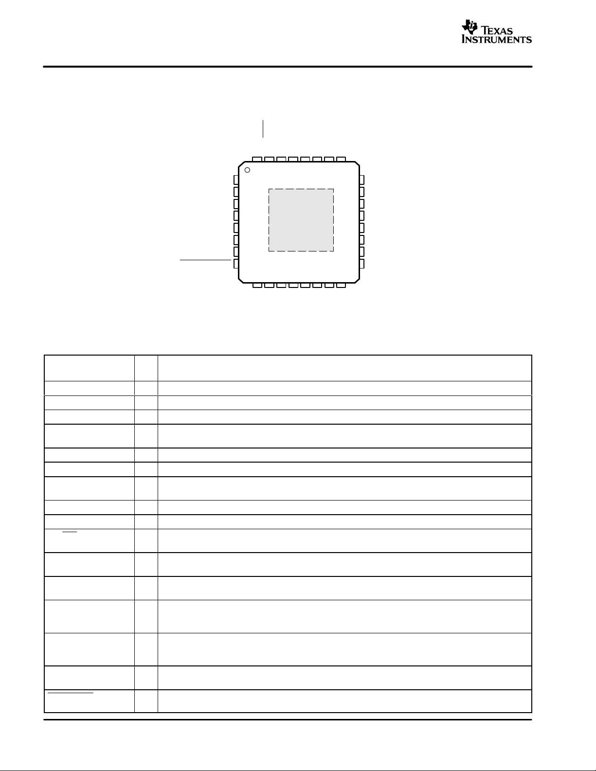
PIN ASSIGNMENTS
www.ti.com
VFP PACKAGE
(TOP VIEW)
AVDD
AGND
ROSC
COSC
AREF
IN+
IN-
SHUTDOWN
PVDD
FREQ
INT/EXT
PVDD
PVDD
31 30 29 28 27
32 26
1
2
3
4
5
6
7
8
PowerPAD
910
11 12 13 14 15
PVDD
FAULT1
FAULT0
PVDD
PVDD
PWM
PWM
H/C
H/C
PWM
25
16
H/C
24
23
22
21
20
19
18
17
PWM
PGND
PGND
PGND
PGND
PGND
PGND
H/C
Terminal Functions
TERMINAL
NAME NO.
AGND 2 Analog ground
AREF 5 O Connect 1 µF capacitor to ground for AREF voltage filtering
AVDD 1 I Analog power supply
COSC 4 I Connect capacitor to ground to set oscillation frequency (220 pF for 500 kHz, 1 nF for 100 kHz) when the internal
FAULT0 10 O Fault flag 0, low when active open drain output (see application information)
FAULT1 9 O Fault flag 1, low when active open drain output (see application information)
FREQ 32 I
IN- 7 I Negative differential input
IN+ 6 I Positive differential input
INT/EXT 31 I Selects the internal oscillator when a TTL logic high is applied to this terminal; selects the use of an external oscil-
H/C 14, 15,
16, 17
PWM 24, 25,
26, 27
PGND 18, 19,
20, 21,
22, 23
PVDD 11, 12,
13, 28,
29, 30
ROSC 3 I Connect 120-kΩ resistor to AGND to set oscillation frequency (either 500 kHz or 100 kHz). Not needed if an
SHUTDOWN 8 I Places the amplifier in shutdown mode when a TTL logic low is applied to this terminal; places the amplifier
I/O DESCRIPTION
oscillator is selected; connect clock signal when an external oscillator is used
Selects 500 kHz switching frequency when a TTL logic low is applied to this terminal; selects 100 kHz switching
frequency when a TTL logic high is applied
lator when a TTL logic low is applied to this terminal
O Direction control output for heat and cool modes (4 pins)
O PWM output for voltage magnitude (4 pins)
High-current ground (6 pins)
I High-current power supply (6 pins)
external clock is used.
in normal operation when a TTL logic high is applied
4
Page 5
www.ti.com
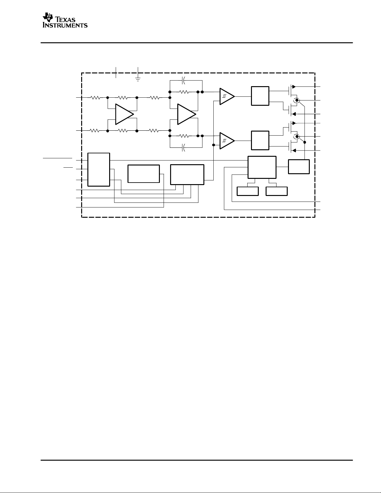
FUNCTIONAL BLOCK DIAGRAM
DRV593
DRV594
SLOS401A - SEPTEMBER 2002 REVISED - OCTOBER 2002
IN-
IN+
SHUTDOWN
INT/EXT
FREQ
COSC
ROSC
AREF
R
R
TTL
Input
Buffer
AVDD
AVDD
AGND
2.3 ×R (DRV593)
14.5 x R (DRV594)
_
+
_
+
2.3 ×R (DRV593)
14.5 x R (DRV594)
Biases
References
and
_
+
_
+
Ramp
Generator
+
_
+
_
Thermal VDDok
Gate
Drive
Gate
Drive
Start-Up
Protection
Logic
PVDD
H/C
PGND
PVDD
PWM
PGND
OC
Detect
FAULT0
FAULT1
5
Page 6
DRV593
)
r
DS(on)
Drain source on state resistance
DRV594
SLOS401A - SEPTEMBER 2002 REVISED - OCTOBER 2002
TYPICAL CHARACTERISTICS
TABLE OF GRAPHS
Efficiency vs Load resistance 2, 3
vs Supply voltage 4
r
DS(on
I
q
PSRR Power supply rejection ratio vs Frequency 8, 9
I
O
V
IO
Drain-source on-state resistance
Supply current vs Supply voltage 7
Closed loop response 12, 13
Maximum output current
Input offset voltage Common-mode input voltage 16, 17
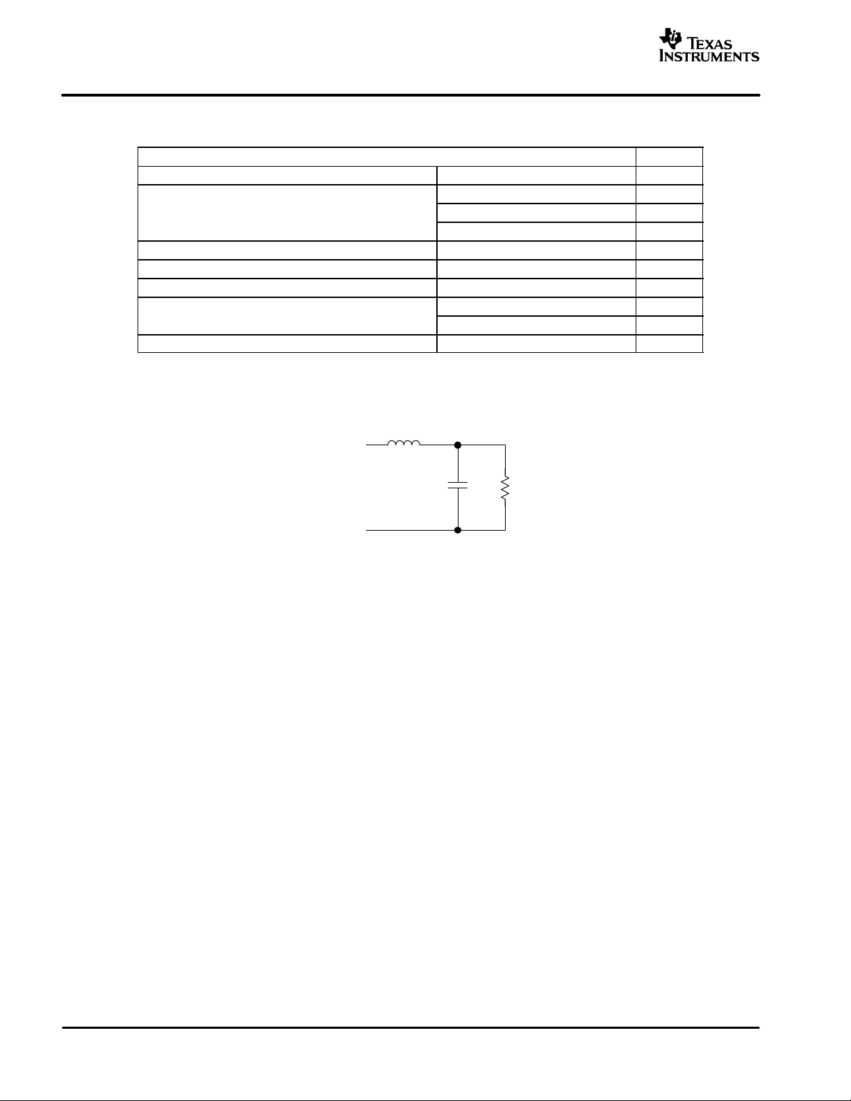
TEST SETUP FOR GRAPHS
The LC output filter used in Figures 2, 3, 8, and 9 is shown below.
L1
PWM
vs Free-air temperature 5
vs Free-air temperature 6
vs Output voltage 14
vs Ambient temperature 15
www.ti.com
FIGURE
C1
H/C
L1 = 10 µH (part number: CDRH104R, manufacturer: Sumida)
C1 = 10 µF (part number: ECJ-4YB1C106K, manufacturer: Panasonic)
R
L
Figure 1. LC Output Filter
6
Page 7
www.ti.com
DRV593
DRV594
SLOS401A - SEPTEMBER 2002 REVISED - OCTOBER 2002
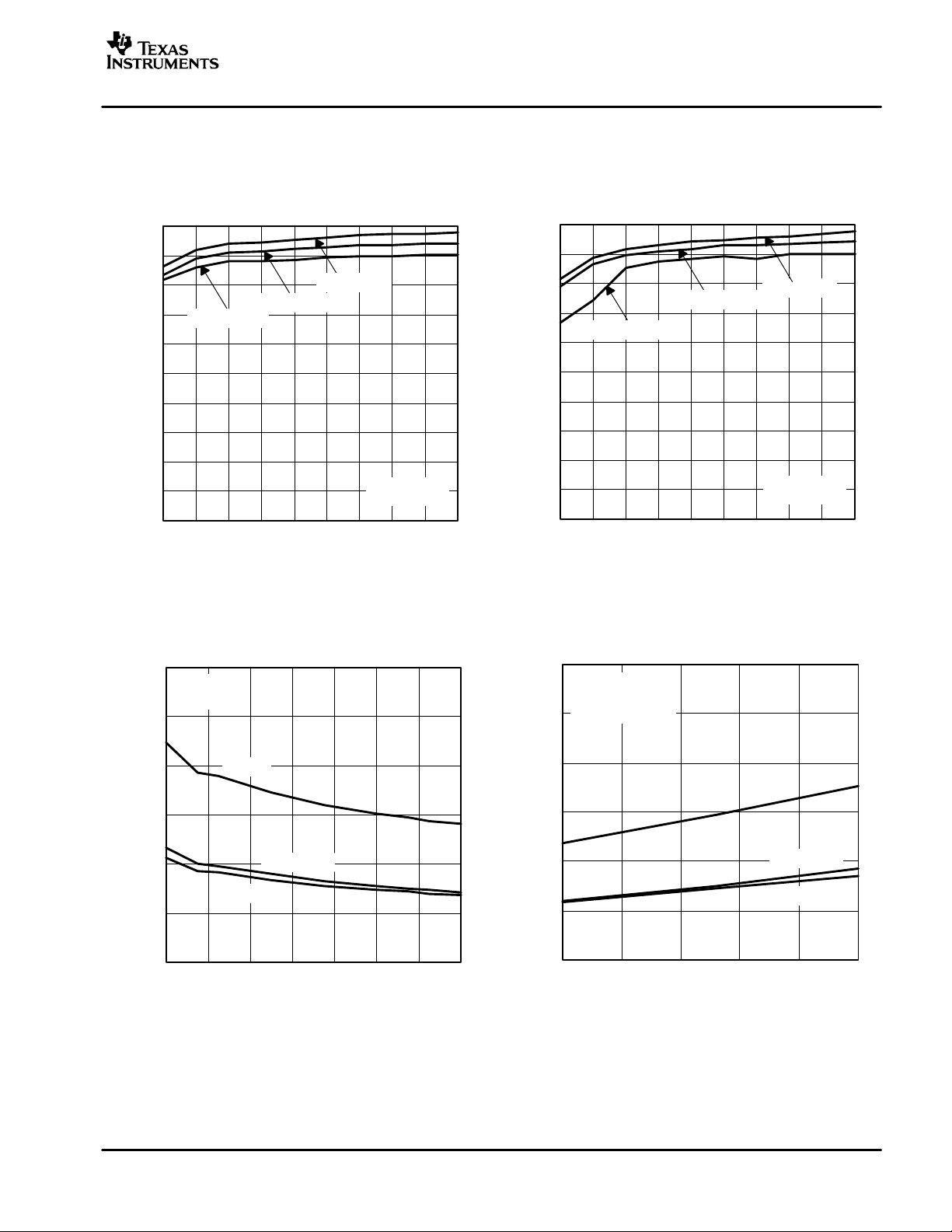
TYPICAL CHARACTERISTICS
EFFICIENCY
vs
LOAD RESISTANCE
100
90
80
70
60
50
40
Efficiency - %
30
20
10
PO = 0.5 W
0
12345678910
PO = 1 W
RL - Load Resistance - Ω
PO = 2 W
VDD = 5 V
fS = 500 kHz
Figure 2
DRAIN-SOURCE ON-STATE RESISTANCE
vs
SUPPLY VOLTAGE
300
IO = 1 A
TA = 25°C
250
EFFICIENCY
vs
LOAD RESISTANCE
100
90
80
70
60
50
40
Efficiency - %
30
20
10
0
PO = 0.25 W
12345678910
RL - Load Resistance - Ω
PO = 0.5 W
PO = 1 W
VDD = 3.3 V
fS = 500 kHz
Figure 3
DRAIN-SOURCE ON-STATE RESISTANCE
vs
FREE-AIR TEMPERATURE
300
VDD = 5 V
IO = 1 A
VFP Package
250
200
150
100
50
- Drain-Source On-State Resistance - mΩ
DS(on)
r
0
2.7 3.1 3.5 3.9 4.3 4.7 5.1 5.5
Total
Low Side
High Side
VDD - Supply Voltage - V
Figure 4
200
Total
150
100
50
- Drain-Source On-State Resistance - mΩ
DS(on)
r
0
-40 -15 10 35 60 85
TA - Free-Air Temperature - °C
Figure 5
Low Side
High Side
7
Page 8

DRV593
DRV594
SLOS401A - SEPTEMBER 2002 REVISED - OCTOBER 2002
TYPICAL CHARACTERISTICS
www.ti.com
DRAIN-SOURCE ON-STATE RESISTANCE
vs
FREE-AIR TEMPERATURE
300
VDD = 3.3 V
IO = 1 A
VFP Package
250
Total
200
150
Low Side
100
High Side
50
- Drain-Source On-State Resistance - mΩ
DS(on)
r
0
-40 -15 10 35 60 85
TA - Free-Air Temperature - °C
Figure 6
SUPPLY CURRENT
vs
SUPPLY VOLTAGE
10
No Load
9
8
7
6
5
4
3
- Supply Current - mA
q
I
2
1
0
2.7 3.1 3.5 3.9 4.3 4.7 5.1 5.5
VDD - Supply Voltage - V
Figure 7
POWER SUPPLY REJECTION RATIO
vs
FREQUENCY
-20
VDD = 5 V
fS = 500 kHz
-30
RL = 1 Ω
V
= 100 mV
ripple
-40
-50
-60
-70
PSRR - Power Supply Rejection Ratio - dB
-80
10 100 1k 10k 100k
pp
f - Frequency - Hz
Figure 8
POWER SUPPLY REJECTION RATIO
vs
FREQUENCY
-20
VDD = 3.3 V
fS = 500 kHz
-30
RL = 1 Ω
V
= 100 mV
ripple
-40
-50
-60
-70
PSRR - Power Supply Rejection Ratio - dB
-80
10 100 1k 10k 100k
pp
f - Frequency - Hz
Figure 9
8
Page 9

www.ti.com
DRV593
DRV594
SLOS401A - SEPTEMBER 2002 REVISED - OCTOBER 2002
TYPICAL CHARACTERISTICS
DRV593
CLOSED LOOP RESPONSE
4
Phase
3
Gain
2
Gain - V/V
1
VDD = 5 V
No Load
0
10 100 1k 10k 100k
f - Frequency - Hz
Figure 10
DRV593
CLOSED LOOP RESPONSE
4
Phase
3
Gain
2
Gain - V/V
1
VDD = 3.3 V
No Load
0
10 100 1k 10k 100k
f - Frequency - Hz
Figure 12
10
0
-10
-20
-30
-40
-50
-60
-70
-80
10
0
-10
-20
-30
-40
-50
-60
-70
-80
DRV594
CLOSED LOOP RESPONSE
16
14
12
Phase
10
8
Phase - °
Gain - V/V
6
4
VDD = 5 V
2
No Load
0
10 100 1 k 10 k 100 k
f - Frequency - Hz
Figure 11
DRV594
CLOSED LOOP RESPONSE
16
14
12
Phase
10
°
8
Phase -
Gain - V/V
6
4
VDD = 3.3 V
2
No Load
0
10 100 1 k 10 k 100 k
f - Frequency - Hz
Figure 13
Gain
Gain
10
0
-10
-20
-30
Phase - °
-40
-50
-60
-70
10
0
-10
-20
-30
Phase - °
-40
-50
-60
-70
9
Page 10

DRV593
DRV594
SLOS401A - SEPTEMBER 2002 REVISED - OCTOBER 2002
TYPICAL CHARACTERISTICS
www.ti.com
MAXIMUM OUTPUT CURRENT
vs
OUTPUT VOLTAGE
3.5
3
TJ = 100°C
2.5
2
1.5
1
- Maximum Output Current - A
O
I
0.5
0
012345
TJ = 125°C
VO - Output Voltage - V
TJ = 85°C
VDD = 5 V
TA = 25°C
VFP Package
Figure 14
INPUT OFFSET VOLTAGE
vs
COMMON-MODE INPUT VOLTAGE
10
VDD = 5 V
No Load
9
MAXIMUM OUTPUT CURRENT
vs
AMBIENT TEMPERATURE
3.5
3
2.5
2
1.5
1
- Maximum Output Current - A
O
I
0.5
TJ ≤ 125°C
VFP Package
0
-40-30-20-100 10203040506070 80
TA - Ambient Temperature - °C
Figure 15
INPUT OFFSET VOLTAGE
vs
COMMON-MODE INPUT VOLTAGE
20
VDD = 3.3 V
No Load
19
10
8
7
6
5
4
3
- Input Offset Voltage - mV
IO
V
2
1
0
1.2 1.6 2.0 2.4 2.8 3.2 3.6 3.8
VIC - Common-Mode Input Voltage - V
Figure 16
18
17
16
15
14
13
- Input Offset Voltage - mV
IO
V
12
11
10
1.2 1.3 1.4 1.5 1.6 1.7 1.8 1.9 2.0 2.1
VIC - Common-Mode Input Voltage - V
Figure 17
Page 11

www.ti.com
SLOS401A - SEPTEMBER 2002 REVISED - OCTOBER 2002
APPLICATION INFORMATION
PULSE-WIDTH MODULATION SCHEME FOR DRV593 AND DRV594
The pulse-width modulation scheme implemented in the DRV593 and DRV594 eliminates one-half of the full output
filter previously required for PWM drivers. The DRV593 and DRV594 require only one inductor and capacitor for the
output filter. The H/C outputs determine the direction of the current and do not switch back and forth. The PWM outputs
switch to produce a voltage across the load that is proportional to the input control voltage.
COOLING MODE
Figure 18 shows the DRV593 and DRV594 in cooling mode. The H/C outputs (pins 14-17) are at ground and the
PWM outputs (pins 24-27) create a voltage across the load that is proportional to the input voltage.
The differential voltage across the load is determined using equation (1) and the duty cycle using equation (2). The
differential voltage is defined as the voltage measured after the filter on the PWM output relative to the H/C output.
DRV593
DRV594
V
D +
Load
A
v
+ D V
ǒ
V
IN)–VIN–
V
DD
DD
Ǔ
where
D duty cycle of the PWM signal
A
V
V
V
Gain of DRV593/594 (DRV593: 2.3 V/V, DRV594: 14.5 V/V)
v
Positive input terminal of the DRV593/594
IN+
Negative input terminal of the DRV593/594
IN -
Power supply voltage
DD
For example, a 50% duty cycle, shown in Figure 18, results in 2.5 V across the load for V
VDD
PWM
0
VDD
DD
(1)
(2)
= 5 V.
H/C
VDD/2
Load
Voltage
0
VDD
0
Figure 18. Cooling Mode
11
Page 12

DRV593
DRV594
SLOS401A - SEPTEMBER 2002 REVISED - OCTOBER 2002
HEATING MODE
Figure 19 shows the DRV593 and DRV594 in heating mode. The H/C output is at VDD and the PWM output is
proportional to the voltage across the load.
The differential voltage across the load is determined using equation (3). The variables are the same as used
previously for equations (1) and (2).
www.ti.com
V
+ –(1–D) V
Load
DD
(3)
For example, a 50% duty cycle, shown in Figure 19, results in -2.5 V across the load for VDD = 5 V. The differential
voltage across the load is defined as the voltage measured after the filter on the PWM output relative to the H/C output.
VDD
PWM
0
VDD
H/C
0
Load
Voltage
0
-VDD/2
12
-VDD
Figure 19. Heating Mode
Page 13

www.ti.com
SLOS401A - SEPTEMBER 2002 REVISED - OCTOBER 2002
HEAT/COOL TRANSITION
As the device transitions from cooling to heating, the duty cycle of the PWM outputs decrease to a small value and
the H/C outputs remains at ground. When the device transitions to heating mode, the H/C outputs change from zero
volts to VDD and the PWM outputs change to a high duty cycle. The direction of the current flow is reversed, but a
low voltage is maintained across the load. The duty cycle decreases as the part is put further into heating mode to
drive more current through the load. Figure 20 illustrates the transition from cooling to heating.
ZERO-CROSSING REGION
When the differential output voltage is near zero, the control logic in the DRV593 and DRV594 causes the outputs
to change between heating and cooling modes. There are two possible states for the PWM and H/C outputs to obtain
zero volts differentially: both outputs can be at VDD or both outputs can be at ground. Therefore, random noise causes
the outputs to change between the two states when the two input voltages are equal. The outputs switch from zero
to VDD, although not at a fixed frequency rate. Some of the pulses may be wider than others, but the two outputs
(PWM and H/C) track each other to provide zero differential voltage. These uneven pulse widths can increase the
switching noise during the zero-crossing condition.
To avoid this phenomenon, hysteresis should be implemented in the control loop to prevent the device from operating
within this region. Although planning for operation during the zero-crossing is important, the normal operating points
for the DRV593 and DRV594 are outside of this region. For laser temperature/wavelength regulation, the zero volts
output condition is only a concern when the laser temperature or wavelength, relative to the ambient temperature,
requires no heating or cooling from the TEC element.
DRV593
DRV594
PWM
H/C
VDD
VDD
VDD
IN +
IN -
0
0
0
Figure 20. Transition From Cooling to Heating
13
Page 14

DRV593
DRV594
SLOS401A - SEPTEMBER 2002 REVISED - OCTOBER 2002
www.ti.com
V
DD
1 µF
PVDD
PVDD
1 µF
PWM
PVDD
PVDD
H/C
PWM
H/C
PWM
PGND
PGND
PGND
PGND
PGND
PGND
H/C
PWM
H/C
10 µH
To TEC or Laser
Diode Anode
10 µF
To TEC or Laser
Diode Cathode
DC Control
Voltage
1 kΩ
1 kΩ
Shutdown Control
1 µF
220 pF
1 µF
FAULT1
FAULT0
120 kΩ
10 µF
PVDD
AVDD
AGND (Connect to PowerPAD)
ROSC
COSC
AREF
IN+
IN-IN-
SHUTDOWN
FREQ
FAULT1
INT/EXT
DRV593
DRV594
FAULT0
PVDD
Figure 21. Typical Application Circuit
OUTPUT FILTER CONSIDERATIONS
TEC element manufacturers provide electrical specifications for maximum dc current and maximum output
voltage for each particular element. The maximum ripple current, however, is typically only recommended to
be less than 10% with no reference to the frequency components of the current. The maximum temperature
differential across the element, which decreases as ripple current increases, may be calculated with the
following equation:
ǒ
1 ) N
1
DT
2
max
Ǔ
DT +
(4)
where
∆T = actual temperature differential
∆T
= maximum temperature differential (specified by manufacturer)
max
N = ratio of ripple current to dc current
According to this relationship, a 10% ripple current reduces the maximum temperature differential by 1%. An
LC network may be used to filter the current flowing to the TEC to reduce the amount of ripple and, more
importantly, protect the rest of the system from any electromagnetic interference (EMI).
FILTER COMPONENT SELECTION
The LC filter, which may be designed from two different perspectives, both described below, helps estimate the
overall performance of the system. The filter should be designed for the worst-case conditions during operation,
which is typically when the differential output is at 50% duty cycle. The following section serves as a starting
point for the design, and any calculations should be confirmed with a prototype circuit in the lab.
Any filter should always be placed as close as possible to the DRV593 and DRV594 to reduce EMI.
L
PWM
C
H/C
Figure 22. LC Output Filter
14
TEC
R
Page 15

www.ti.com
SLOS401A - SEPTEMBER 2002 REVISED - OCTOBER 2002
LC FILTER IN THE FREQUENCY DOMAIN
The transfer function for a second-order low-pass filter (Figures 17 and 18) is shown in equation (5):
DRV593
DRV594
HLP(jw) +
w
ǒ
–
w
w0+
For the DRV593 and DRV594, the differential output switching frequency is typically selected to be 500 kHz.
The resonant frequency for the filter is typically chosen to be at least one order of magnitude lower than the
switching frequency. equation (5) may then be simplified to give the following magnitude equation (6). These
equations assume the use of the filter in Figure 22.
Ť
If L=10 µH and C=10 µF, the cutoff frequency is 15.9 kHz, which corresponds to –60 dB of attenuation at the
500 kHz switching frequency. For VDD = 5 V, the amount of ripple voltage at the TEC element is approximately
5 mV.
The average TEC element has a resistance of 1.5 Ω, so the ripple current through the TEC is approximately
3.4 mA. At the 3-A maximum output current of the DRV593 and DRV594, this 5.4 mA corresponds to 0.11%
ripple current, causing less than 0.0001% reduction of the maximum temperature differential of the TEC
element (see equation 4).
1
Ǹ
LC
Q + quality factor
w + DRV593 or DRV594 switching frequency
H
LPŤdB
f
fs+ 500 kHz (DRV593 or DRV594 switching frequency)
+
o
+ –40 log
1
Ǹ
2p LC
1
2
Ǔ
0
)
jw
1
) 1
w
Q
0
f
s
ǒ
Ǔ
f
o
(5)
(6)
LC FILTER IN THE TIME DOMAIN
The ripple current of an inductor may be calculated using equation (7):
ǒ
VO–V
DI
+
L
D + duty cycle (0.5 worst case)
Ts+ 1ńfs+ 1ń500 kHz
For VO = 5 V, V
ripple current flows through the TEC element, however, the properties of the filter capacitor must be considered.
For relatively small capacitors (less than 22 µF) with very low equivalent series resistance (ESR, less than
10 mΩ), such as ceramic capacitors, the following equation (8) may be used to estimate the ripple voltage on
the capacitor due to the change in charge:
DV
= 2.5 V, and L = 10 µH, the inductor ripple current is 250 mA. To calculate how much of that
TEC
2
p
+
C
2
D + duty cycle
fs+ 500 kHz
f
+
o
2p LC
ǒ
1–D
1
Ǹ
TEC
L
Ǔ
DT
s
2
f
o
Ǔ
ǒ
Ǔ
V
TEC
f
s
(7)
(8)
15
Page 16

DRV593
DRV594
SLOS401A - SEPTEMBER 2002 REVISED - OCTOBER 2002
For L = 10 µH and C = 10 µF, the cutoff frequency, fo, is 15.9 kHz. For worst case duty cycle of 0.5 and
=2.5 V, the ripple voltage on the capacitors is 6.2 mV. The ripple current may be calculated by dividing the
V
TEC
ripple voltage by the TEC resistance of 1.5 Ω, resulting in a ripple current through the TEC element of 4.1 mA.
Note that this is similar to the value calculated using the frequency domain approach.
For larger capacitors (greater than 22 µF) with relatively high ESR (greater than 100 mΩ), such as electrolytic
capacitors, the ESR dominates over the charging/discharging of the capacitor. The following simple
equation (9) may be used to estimate the ripple voltage:
www.ti.com
DVC+ DIL R
DIL+ inductor ripple current
R
+ filter capacitor ESR
ESR
ESR
For a 100 µF electrolytic capacitor, an ESR of 0.1 Ω is common. If the 10 µH inductor is used, delivering 250 mA
of ripple current to the capacitor (as calculated above), then the ripple voltage is 25 mV. This is over ten times
that of the 10 µF ceramic capacitor, as ceramic capacitors typically have negligible ESR.
SWITCHING FREQUENCY CONFIGURATION: OSCILLATOR COMPONENTS R
OSC
AND C
AND FREQ OPERATION
The onboard ramp generator requires an external resistor and capacitor to set the oscillation frequency. The
frequency may be either 500 kHz or 100 kHz by selecting the proper capacitor value and by holding the FREQ
pin either low (500 kHz) or high (100 kHz). Table 1 shows the values required and FREQ pin configuration for
each switching frequency.
Table 1. Frequency Configuration Options
SWITCHING FREQUENCY R
500 kHz 120 kΩ 220 pF LOW (GND)
100 kHz 120 kΩ 1 nF HIGH (VDD)
For proper operation, the resistor R
should have 1% tolerance while capacitor C
OSC
OSC
type with 10% tolerance. Both components should be grounded to AGND, which should be connected to PGND
at a single point, typically where power and ground are physically connected to the printed-circuit board.
C
OSC
FREQ
should be a ceramic
OSC
(9)
OSC
EXTERNAL CLOCKING OPERATION
To synchronize the switching to an external clock signal, pull the INT/EXT terminal low, and drive the clock signal
into the COSC terminal. This clock signal must be from 10% to 90% duty cycle and meet the voltage
requirements specified in the electrical specifications table. Since the DRV593 and DRV594 include an internal
frequency doubler, the external clock signal must be approximately 250 kHz. Deviations from the 250 kHz clock
frequency are allowed and are specified in the electrical characteristic table. The resistor connected from ROSC
to ground may be omitted from the circuit in this mode of operation—the source is disconnected internally.
INPUT CONFIGURATION: DIFFERENTIAL AND SINGLE-ENDED
If a differential input is used, it should be biased around the midrail of the DRV593 or DRV594 and must not
exceed the common-mode input range of the input stage (see the operating characteristics at the beginning
of the data sheet).
The most common configuration employs a single-ended input. The unused input should be tied to VDD/2, which
may be simply accomplished with a resistive voltage divider. For the best performance, the resistor values
chosen should be at least 100 times lower than the input resistance of the DRV593 or DRV594. This prevents
the bias voltage at the unused input from shifting when the signal input is applied. A small ceramic capacitor
should also be placed from the input to ground to filter noise and keep the voltage stable. An op amp configured
as a buffer may also be used to set the voltage at the unused input.
16
Page 17

www.ti.com
FIXED INTERNAL GAIN
The differential output voltage may be calculated using equation (10):
DRV593
DRV594
SLOS401A - SEPTEMBER 2002 REVISED - OCTOBER 2002
VO+ V
AV is the voltage gain, which is fixed internally at 2.3 V/V for DRV593 and 14.5 V/V for DRV594. The maximum
and minimum ratings are provided in the electrical specification table at the beginning of the data sheet.
OUT)–VOUT–
+ A
ǒ
V
v
IN)–VIN–
Ǔ
POWER SUPPLY DECOUPLING
To reduce the effects of high-frequency transients or spikes, a small ceramic capacitor, typically 0.1 µF to 1 µF,
should be placed as close to each set of PVDD pins of the DRV593 and DRV594 as possible. For bulk
decoupling, a 1 0 µF to 100 µF tantalum or aluminum electrolytic capacitor should be placed relatively close to
the DRV593 and DRV594.
AREF CAPACITOR
The AREF terminal is the output of an internal mid-rail voltage regulator used for the onboard oscillator and ramp
generator. The regulator may not be used to provide power to any additional circuitry. A 1 µF ceramic capacitor
must be connected from AREF to AGND for stability (see oscillator components above for AGND connection
information).
SHUTDOWN OPERATION
The DRV593 and DRV594 include a shutdown mode that disables the outputs and places the device in a low
supply current state. The SHUTDOWN pin may be controlled with a TTL logic signal. When SHUTDOWN is
held high, the device operates normally. When SHUTDOWN is held low, the device is placed in shutdown. The
SHUTDOWN pin must not be left floating. If the shutdown feature is unused, the pin may be connected to VDD.
(10)
FAULT REPORTING
The DRV593 and DRV594 include circuitry to sense three faults:
D Overcurrent
D Undervoltage
D Overtemperature
These three fault conditions are decoded via the FAULT1 and FAULT0 terminals. Internally, these are
open-drain outputs, so an external pullup resistor of 5 kΩ or greater is required.
Table 2. Fault Indicators
FAULT1 FAULT0
0 0 Overcurrent
1 0 Undervoltage
0 1 Overtemperature
1 1 Normal operation
The overcurrent fault is reported when the output current exceeds four amps. As soon as the condition is
sensed, the overcurrent fault is set and the outputs go into a high-impedance state for approximately 3 µs to
5 µs (500 kHz operation). After 3 µs to 5 µs, the outputs are re-enabled. If the overcurrent condition has ended,
the fault is cleared and the device resumes normal operation. If the overcurrent condition still exists, the above
sequence repeats.
The undervoltage fault is reported when the operating voltage is reduced below 2.8 V . This fault is not latched,
so as soon as the power supply recovers, the fault is cleared and normal operation resumes. During the
undervoltage condition, the outputs go into a high-impedance state to prevent overdissipation due to increased
r
.
DS(on)
17
Page 18

DRV593
DRV594
SLOS401A - SEPTEMBER 2002 REVISED - OCTOBER 2002
The overtemperature fault is reported when the junction temperature exceeds 115°C. The device continues
operating normally until the junction temperature reaches 150°C, at which point the IC is disabled to prevent
permanent damage from occurring. The system’s controller must reduce the power demanded from the
DRV593 o r D R V594 once the overtemperature flag is set, or else the device switches of f when it reaches 150°C.
This fault is not latched; once the junction temperature drops below 115°C, the fault is cleared, and normal
operation resumes.
POWER DISSIPATION AND MAXIMUM AMBIENT TEMPERATURE
Though the DRV593 and DRV594 are much more efficient than traditional linear solutions, the power drop
across the on-resistance of the output transistors does generate some heat in the package, which may be
calculated as shown in equation (11):
www.ti.com
I
OUT
ǒ
2
Ǔ
r
DS(on), total
θ
P
JA
DISS
Ǔ
P
DISS
For example, at the maximum output current of 3 A through a total on-resistance of 130 mΩ (at TJ = 25°C),
the power dissipated in the package is 1.17 W.
Calculate the maximum ambient temperature using equation (12):
TA+ T
+
ǒ
*
J
PRINTED-CIRCUIT BOARD (PCB) LAYOUT CONSIDERATIONS
Since the DRV593 and DRV594 are high-current switching devices, a few guidelines for the layout of the
printed-circuit board (PCB) must be considered:
1. Grounding. Analog ground (AGND) and power ground (PGND) must be kept separated, ideally back to
where the power supply physically connects to the PCB, minimally back to the bulk decoupling capacitor
(10 µF ceramic minimum). Furthermore, the PowerPAD ground connection should be made to AGND, not
PGND. Ground planes are not recommended for AGND or PGND, traces should be used to route the
currents. Wide traces (100 mils) should be used for PGND while narrow traces (15 mils) should be used
for AGND.
2. Power supply decoupling. A small 0.1 µF to 1 µF ceramic capacitor should be placed as close to each
set of PVDD pins as possible, connecting from PVDD to PGND. A 0.1 µF to 1 µF ceramic capacitor should
also be placed close to the AVDD pin, connecting from AVDD to AGND. A bulk decoupling capacitor of at
least 10 µF, preferably ceramic, should be placed close to the DRV593 or DRV594, from PVDD to PGND.
If power supply lines are long, additional decoupling may be required.
(11)
(12)
3. Power and output traces. The power and output traces should be sized to handle the desired maximum
output current. The output traces should be kept as short as possible to reduce EMI, i.e., the output filter
should be placed as close to the DRV593 or DRV594 outputs as possible.
4. PowerPAD. The DRV593 and DRV594 in the Quad Flatpack package use TI’s PowerPAD technology to
enhance the thermal performance. The PowerPAD is physically connected to the substrate of the DRV593
and DRV594 silicon, which is connected to AGND. The PowerPAD ground connection should therefore be
kept separate from PGND as described above. The pad underneath the AGND pin may be connected
underneath the device to the PowerPAD ground connection for ease of routing. For additional information
on PowerPAD PCB layout, refer to the PowerPAD Thermally Enhanced Package application note,
SLMA002.
5. Thermal performance. For proper thermal performance, the PowerPAD must be soldered down to a
thermal land, as described in the PowerPAD Thermally Enhanced Package application note, SLMA002.
In addition, at high current levels (greater than 2 A) or high ambient temperatures (greater than 25°C), an
internal plane may be used for heat sinking. The vias under the PowerPAD should make a solid connection,
and the plane should not be tied to ground except through the PowerPAD connection, as described above.
18
Page 19

DRV593
www.ti.com
SLOS401A - SEPTEMBER 2002 REVISED - OCTOBER 2002
MECHANICAL DATA
VFP (S-PQFP-G32) PowerPAD PLASTIC QUAD FLATPACK
DRV594
25
32
1,45
1,35
0,80
24
0,45
0,30
17
16
9
1
5,60 TYP
7,20
SQ
6,80
9,20
SQ
8,80
8
0,22
M
Thermal Pad
(See Note D)
0,05 MIN
0,13 NOM
Gage Plane
0,25
0°-7°
1,60 MAX
NOTES: A. All linear dimensions are in millimeters.
B. This drawing is subject to change without notice.
C. Body dimensions do not include mold flash or protrusion.
D. The package thermal performance may be enhanced by bonding the thermal pad to an external thermal plane.
This pad is electrically and thermally connected to the backside of the die and possibly selected leads.
E. Falls within JEDEC MS-026
PowerPAD is a trademark of Texas Instruments.
Seating Plane
0,10
0,75
0,45
4200791/A 04/00
19
Page 20

PACKAGE OPTION ADDENDUM
www.ti.com
4-Mar-2005
PACKAGING INFORMATION
Orderable Device Status
(1)
Package
Type
Package
Drawing
Pins Package
Qty
Eco Plan
DRV593VFP ACTIVE HLQFP VFP 32 250 None CU NIPDAU Level-1-235C-UNLIM
DRV593VFPR ACTIVE HLQFP VFP 32 1000 None CU NIPDAU Level-1-235C-UNLIM
DRV594VFP ACTIVE HLQFP VFP 32 250 None CU NIPDAU Level-1-235C-UNLIM
DRV594VFPR ACTIVE HLQFP VFP 32 1000 None CU NIPDAU Level-1-235C-UNLIM
(1)
The marketing status values are defined as follows:
ACTIVE: Product device recommended for new designs.
LIFEBUY: TI has announced that the device will be discontinued, and a lifetime-buy period is in effect.
NRND: Not recommended for new designs. Device is in production to support existing customers, but TI does not recommend using this part in
a new design.
PREVIEW: Device has been announced but is not in production. Samples may or may not be available.
OBSOLETE: TI has discontinued the production of the device.
(2)
Eco Plan - May not be currently available - please check http://www.ti.com/productcontent for the latest availability information and additional
product content details.
None: Not yet available Lead (Pb-Free).
Pb-Free (RoHS): TI's terms "Lead-Free" or "Pb-Free" mean semiconductor products that are compatible with the current RoHS requirements
for all 6 substances, including the requirement that lead not exceed 0.1% by weight in homogeneous materials. Where designed to be soldered
at high temperatures, TI Pb-Free products are suitable for use in specified lead-free processes.
Green (RoHS & no Sb/Br): TI defines "Green" to mean "Pb-Free" and in addition, uses package materials that do not contain halogens,
including bromine (Br) or antimony (Sb) above 0.1% of total product weight.
(2)
Lead/Ball Finish MSL Peak Temp
(3)
(3)
MSL, Peak Temp. -- The Moisture Sensitivity Level rating according to the JEDECindustry standard classifications, and peak solder
temperature.
Important Information and Disclaimer:The information provided on this page represents TI's knowledge and belief as of the date that it is
provided. TI bases its knowledge and belief on information provided by third parties, and makes no representation or warranty as to the
accuracy of such information. Efforts are underway to better integrate information from third parties. TI has taken and continues to take
reasonable steps to provide representative and accurate information but may not have conducted destructive testing or chemical analysis on
incoming materials and chemicals. TI and TI suppliers consider certain information to be proprietary, and thus CAS numbers and other limited
information may not be available for release.
In no event shall TI's liability arising out of such information exceed the total purchase price of the TI part(s) at issue in this document sold by TI
to Customer on an annual basis.
Addendum-Page 1
Page 21

Page 22

IMPORTANT NOTICE
Texas Instruments Incorporated and its subsidiaries (TI) reserve the right to make corrections, modifications,
enhancements, improvements, and other changes to its products and services at any time and to discontinue
any product or service without notice. Customers should obtain the latest relevant information before placing
orders and should verify that such information is current and complete. All products are sold subject to TI’s terms
and conditions of sale supplied at the time of order acknowledgment.
TI warrants performance of its hardware products to the specifications applicable at the time of sale in
accordance with TI’s standard warranty. Testing and other quality control techniques are used to the extent TI
deems necessary to support this warranty . Except where mandated by government requirements, testing of all
parameters of each product is not necessarily performed.
TI assumes no liability for applications assistance or customer product design. Customers are responsible for
their products and applications using TI components. To minimize the risks associated with customer products
and applications, customers should provide adequate design and operating safeguards.
TI does not warrant or represent that any license, either express or implied, is granted under any TI patent right,
copyright, mask work right, or other TI intellectual property right relating to any combination, machine, or process
in which TI products or services are used. Information published by TI regarding third-party products or services
does not constitute a license from TI to use such products or services or a warranty or endorsement thereof.
Use of such information may require a license from a third party under the patents or other intellectual property
of the third party, or a license from TI under the patents or other intellectual property of TI.
Reproduction of information in TI data books or data sheets is permissible only if reproduction is without
alteration and is accompanied by all associated warranties, conditions, limitations, and notices. Reproduction
of this information with alteration is an unfair and deceptive business practice. TI is not responsible or liable for
such altered documentation.
Resale of TI products or services with statements different from or beyond the parameters stated by TI for that
product or service voids all express and any implied warranties for the associated TI product or service and
is an unfair and deceptive business practice. TI is not responsible or liable for any such statements.
Following are URLs where you can obtain information on other Texas Instruments products and application
solutions:
Products Applications
Amplifiers amplifier.ti.com Audio www.ti.com/audio
Data Converters dataconverter.ti.com Automotive www.ti.com/automotive
DSP dsp.ti.com Broadband www.ti.com/broadband
Interface interface.ti.com Digital Control www.ti.com/digitalcontrol
Logic logic.ti.com Military www.ti.com/military
Power Mgmt power.ti.com Optical Networking www.ti.com/opticalnetwork
Microcontrollers microcontroller.ti.com Security www.ti.com/security
Telephony www.ti.com/telephony
Video & Imaging www.ti.com/video
Wireless www.ti.com/wireless
Mailing Address: Texas Instruments
Post Office Box 655303 Dallas, Texas 75265
Copyright 2005, Texas Instruments Incorporated
 Loading...