

Texas Instruments CD74HCU04M, CD74HCU04E, CD74HCU04M96 Datasheet
Data sheet acquired from Harris Semiconductor
/
j
SCHS127
February 1998
CD74HCU04
High Speed CMOS Logic
Hex Inverter
[ /Title
(CD74
HCU04
)
Sub-
ect
(High
Speed
CMOS
Logic
Hex
Inverter
Features
• Typical Propagation Delay: 6ns at VCC = 5V,
C
= 15pF, TA = 25oC, Fastest Part in QMOS Line
L
o
• Wide Operating Temperature Range . . . -55
• Balanced Propagation Delay and Transition Times
• Significant Power Reduction Compared to LSTTL
Logic ICs
• HCU Types
- 2V to 6V Operation
- High Noise Immunity: N
V
at VCC = 5V
CC
• CMOS Input Compatibility, I
= 20%, NIH = 30% of
IL
≤ 1µA at VOL, V
l
C to 125oC
OH
Pinout
Description
The Harris CD74HCU04 unbuffered hexinverter utilizes silicongate CMOS technology to achieve operation speeds similar to
LSTTL gates with the low power consumption of standard
CMOS integrated circuits. These devices are especially useful
in crystal oscillator and analog applications. Figures 10 and 11
are supplied as design information for the above applications .
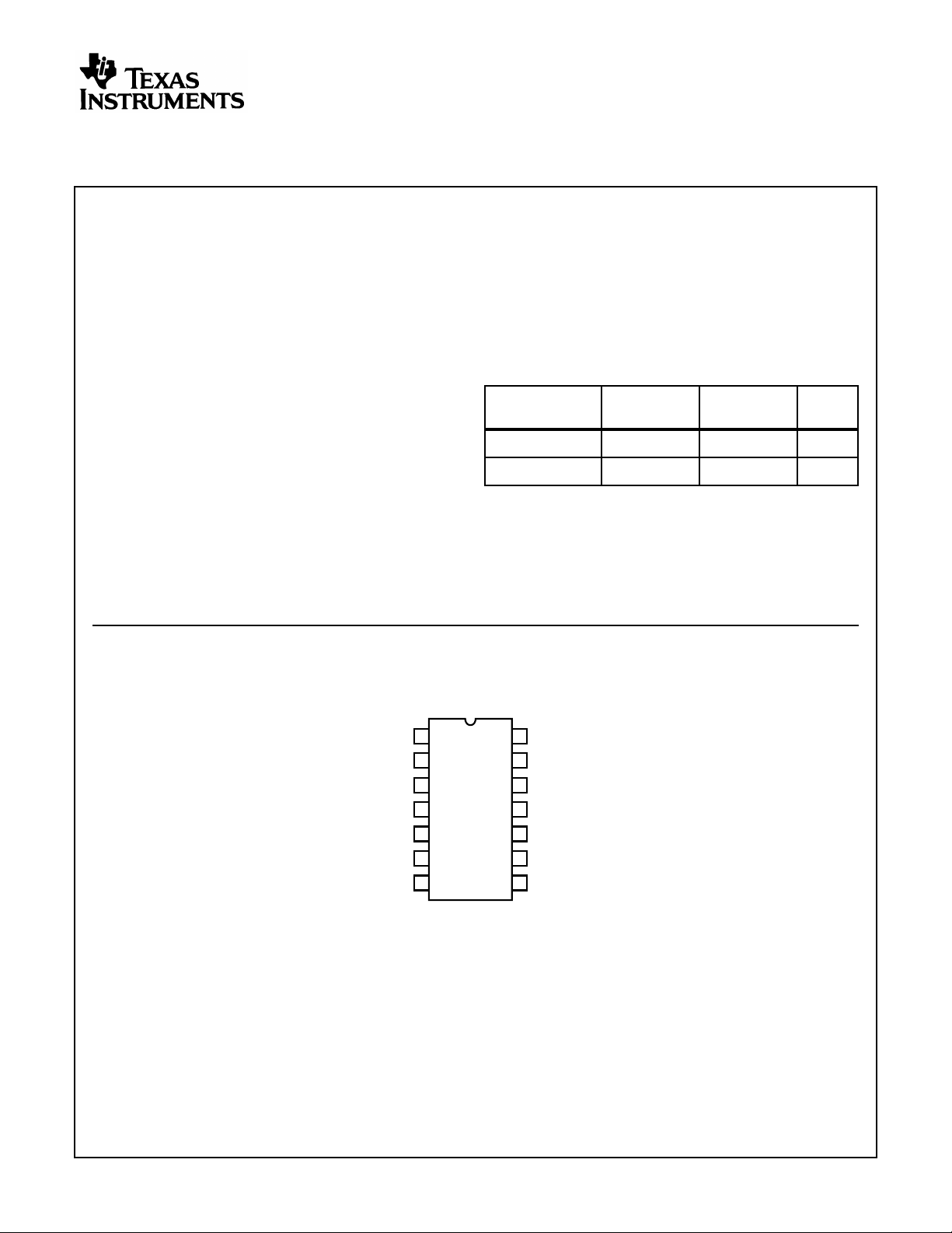
Ordering Information
TEMP.RANGE
PART NUMBER
CD74HCU04E -55 to 125 14 Ld PDIP E14.3
CD74HCU04M -55 to 125 14 Ld SOIC M14.15
NOTES:
1. When ordering, use theentire part number. Add thesuffix 96 to
obtain the variant in the tape and reel.
2. Waferor dieforthis partnumber is availablewhich meetsallelectrical specifications. Please contact your local sales office or
Harris customer service for ordering information.
(oC) PACKAGE
PKG.
NO.
1A
1Y
2A
2Y
3A
3Y
GND
CD74HC04,
(PDIP, SOIC)
TOP VIEW
1
2
3
4
5
6
7
14
V
CC
6A
13
12
6Y
5A
11
5Y
10
4A
9
4Y
8
CAUTION: These devices are sensitive to electrostatic discharge. Users should follow proper IC Handling Procedures.
Copyright
© Harris Corporation 1998
1
File Number 1655.1
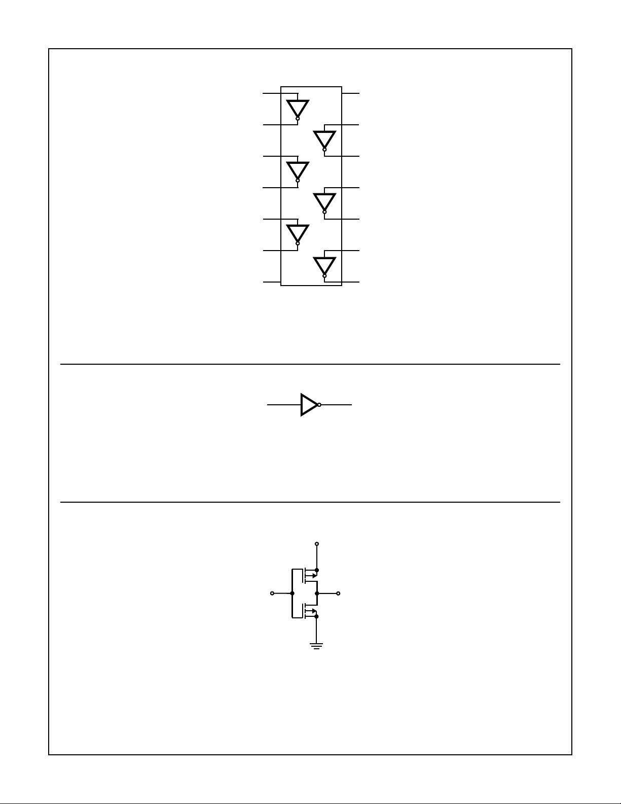
Functional Diagram
CD74HCU04
Logic Symbol
1A
1Y
2A
2Y
3A
3Y
GND
1
2
3
4
5
6
7
14
V
CC
13
6A
12
6Y
11
5A
10
5Y
9
4A
8
4Y
Schematic Diagram
nA nY
(3, 5, 9, 11, 13) 1
V
CC
2 (4, 6, 8, 10, 12)
2
 Loading...