

Page 1
®
VN330SP
QUAD HIGH SIDE SMART
POWER S OL ID S TATE RELAY
TYPE V
VN330SP VCC-55V 0.32Ω (**) 0.7A 36 V
(*) Per channel
(**) at Tj=85°C
n
OUTPUT CURRENT: 0.7A PER CHANNEL
n
DIGITAL INPUTS CLAMPED AT 32V MINIMUM
demag
(*) R
DSon
(*) I
out
(*) V
cc
VOLTAGE
n
SHORTED LOAD AND O VERTEMPERATURE
PROTECTIONS
n
BUILT-IN CURRENT LIM ITER
n
UNDERVOLTAGE SHUT-DOWN
n
OPEN DRAIN DIAGNOSTIC OUTPUT
n
FAST DEMAGNETIZATION OF INDUCTIVE
LOADS
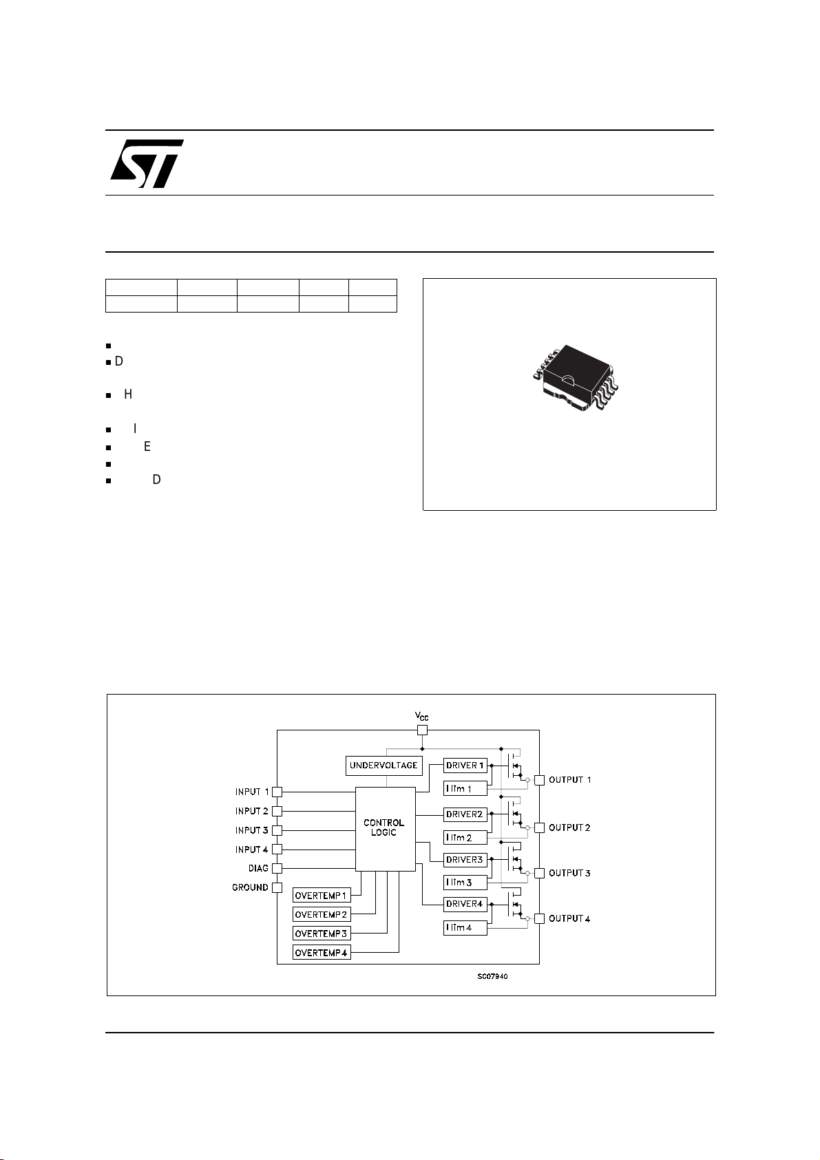
DESCRIPTION
The VN330SP is a mono lithic device m ade using
STMicroelectronics VIPower technology, intended
for drivi ng four indipendent r esistive or induct ive
loads with one side conne cted to ground. Active
current limitation avoids dropping the system
power supply in case of shorted load. Built-in
thermal shut-down protects the chip from
BLOCK DIAGRAM
10
1
PowerSO-10
TM
overtemperature and short circuit. The open drain
diagnostic output indicates short circuit and
overtemperature conditions.
August 2000 1/9
1
1
Page 2
VN330SP
ABSOLUTE MAXIMUM RATI NG
Symbol Parameter Value Unit
CC
CC
R
IN
AS
tot
stg
Power supply voltage 45 V
Reverse supply voltage -0.3 V
Output current (continuous) Internally limited A
Reverse output current (per channel) -6 A
Input current (per chan nel) ± 10 mA
Diag pin current ±10 mA
Electrostatic discharge (R=1.5KΩ; C=100pF) 2000 V
Single pul se avalan che energy per channel not simultaneously
(see figure 1)
400 mJ
Power dissipation at Tc ≤ 25°C Internally limited W
Junction operating temperature Internally limited °C
j
Storage temperature -55 to 150 °C
V
-V
I
OUT
I
I
I
DIAG
V
ESD
E
P
T
T
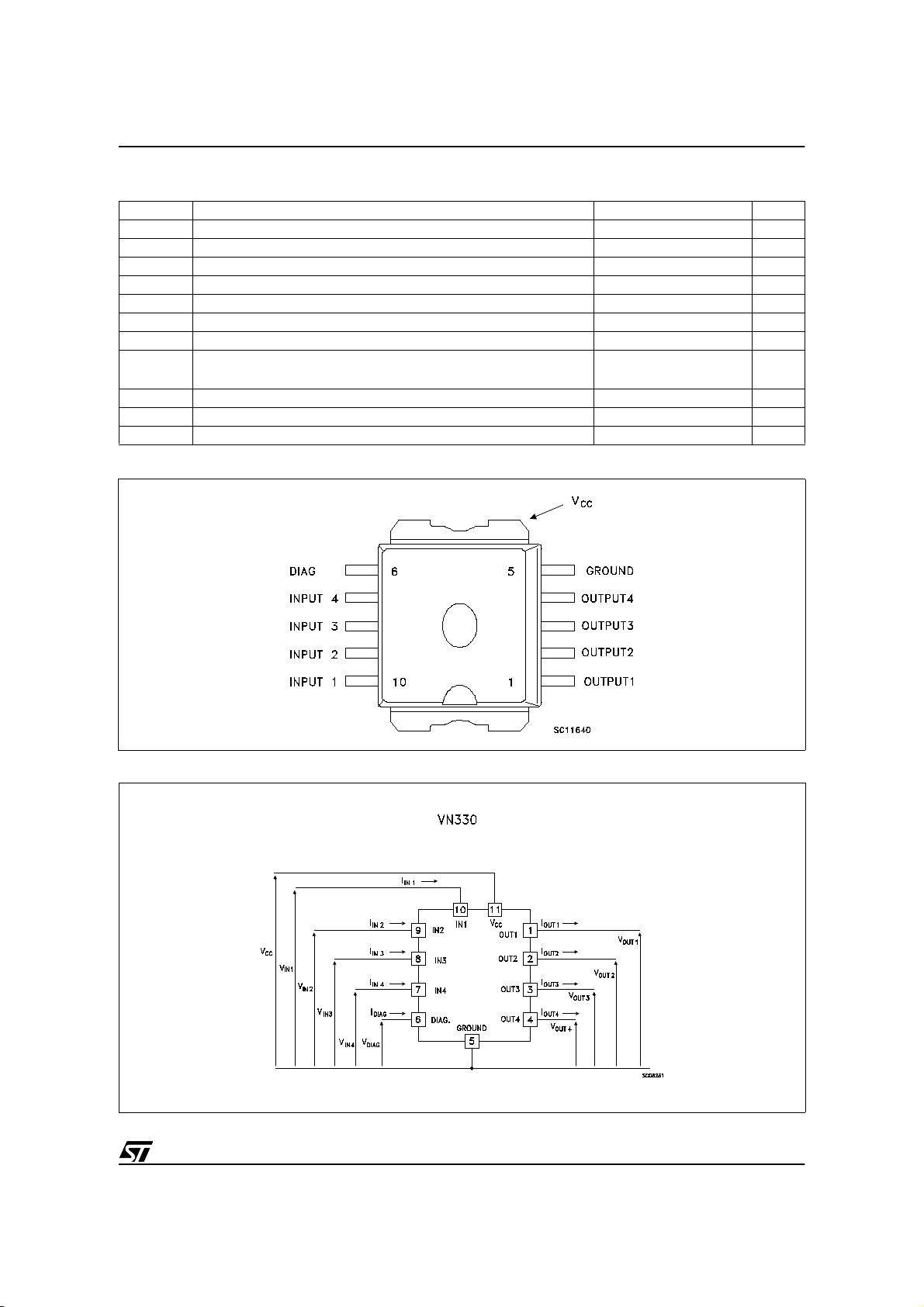
CONNECTION DIAGRAM TOP VIEW
CURRENT AND VOLTAGE CONVENTIONS
2/9
1
Page 3
VN330SP
THERMAL DATA
Symbol Parameter Value Unit
CC
ON
S
t
r
t
f
Thermal resistance junction -case (1) (MAX) 2 °C/W
Thermal resistance junction-ambient ($) (MAX) 50 °C/W
Supply voltage 10 36 V
On state resistance
Supply current
Output voltage at turn-off I
Turn-on delay tim e of ou t put current
Rise time of output
current
Turn-off delay time of
output current
Fall time of output current
Turn-on current slope
on
Turn-off current slope
off
=0.5A; Tj=125°C
I
OUT
I
=0.5A; Tj=85°C
OUT
All channels off
On state; T
OUT
I
OUT
=125°C; I
j
=0.5A; L
=1mH VCC-65 VCC-55 VCC-45 V
LOAD
=0.5A, Resistive Load
Input rise time <0.1µs
T
=25°C
j
T
=125°C
j
I
=0.5A, Resistive Load
OUT
Input rise time <0.1µs
T
=25°C
j
T
=125°C
j
I
=0.5A, Resistive Load
OUT
Input rise time <0.1µs
T
=25°C
j
T
=125°C
j
I
=0.5A, Resistive Load
OUT
Input rise time <0.1µs
T
=25°C
j
T
=125°C
j
=0.5A
I
OUT
I
OUT=ILIM
I
OUT
I
OUT=ILIM
; Tj=25°C
=0.5A
; Tj=25°C
OUTn
=0V
30 40
50 100
20 30
81520µs
0.4
0.32
115
0.5
1
10
60
40
2
2
4
R
thj-case
R
thj-amb
(1) All channels ON
($) When mounted using minimum recommended pad size on FR-4 board
ELECTRICAL CHARACTERISTICS (10V<VCC<36V; -25°C<Tj<125°C; unless otherwise specified)
POWER
Symbol Parameter Test Conditions Min Typ Max Unit
V
R
I
V
demag
SWITCHING (VCC=24V)
Symbol Parameter Test Conditions Min Typ Max Unit
t
d(on)
t
d(off)
(di/dt)
(di/dt)
Ω
Ω
mA
mA
µs
µs
µs
µs
µs
µs
µs
A/µs
A/µs
A/µs
A/µs
3/9
1
Page 4
VN330SP
ELECTRICAL CHARACTERISTICS (continued)
LOGIC INPUT (Per each channel)
Symbol Parameter Test Conditions Min Typ Max Unit
V
V
V
I(HYST)
I
I
LGND
V
Note 1: The input voltage is internally clamped at 32V minimum, it is possible to connect the input pins to an higher voltage via an external
resistor calculate to not exc eed 10mA.
PROTECTION AND DIAGNOSTICS
Symbol Parameter Test Conditions Min Typ Max Unit
V
DIAG
V
SCL
V
USD
V
I
LIM
I
OVPK
I
DIAGH
I
LOAD
t
SC
T
TSD
T
(*) Status determination > 100µs after the swit c hing edge.
Note: If INPUT pin is left floating the corrisponding channel will automatically switch off. If GND pin is disconnected, all channels will switch
off provide d V
Input low level voltage 2 V
IL
Input high level voltage
IH
(see note 1)
Input hysteresis voltage 0.5 V
Inpu t curre n t
IN
Output current in gr ound
disconnection
Inpu t clamp voltag e
ICL
(see note 1)
(*) Stat us voltage output low I
Status clamp voltage I
(*)
Undervolt age shut down 5 8 V
Low state output voltage VIN=V
OL
DC Short circuit current VCC=24V; R
Peak short circuit current
Leakage on diag pin in
high state
Output leakage current VCC=10 to 36V; VIN=V
Delay time of current
limiter
Thermal shut down
temperature
Reset temperature 135 155 °C
R
does not exceed 36V.
CC
3.5 V
V
= 0 to 30V
IN
V
= 0 to 2V 25
IN
VCC=V
IIN=1mA
I
IN
STAT
DIAG
I
DIAG
V
=GND=DIAG=24V; Tj=25°C 25 mA
INn
32 36
=-1mA
-0.7
=5mA (Fault condition) 1 V
=1mA
=-1mA
; R
ILj
LOAD
LOAD
=24V; VIN=30V; R
CC
≥10MΩ 1.5 V
<10mΩ 0.7 2.5 A
<10mΩ
LOAD
32 36
-0.7
(see figure 2)
V
=24V 100 µA
DIAG
IL
150 170 °C
600 µA
µA
V
V
V
V
4A
50 µA
100 µs
4/9
2
Page 5

VN330SP
FIGURE 1: Avalanche Energy Test Circuit
FIGURE 2: Peak Short Circuit Current Test Circuit
5/9
1
Page 6
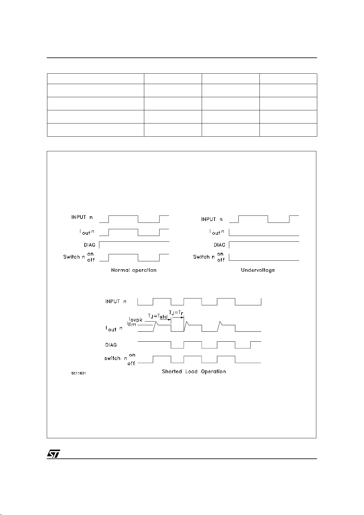
THRUTH TABLE
Normal operation L
Overtemperature L
Undervoltage L
Shorted load
(Current limitation)
Figur e 3: Switching Waveforms
VN330SP
INPUTn OUTPUTn DIAGNOSTIC
H
H
H
L
H
L
H
L
L
L
L
L
H
H
H
H
L
H
H
H
H
6/9
1
Page 7

VN330SP
SWITCHING PARAMETERS TEST CONDITIONS
DRIVING CIRCUIT
7/9
2
Page 8

PowerSO-10™ MECHANICAL DATA
VN330SP
DIM.
MIN. TYP MAX. MIN. TYP. MAX.
mm. inch
A 3.35 3.65 0.132 0.144
A (*) 3.4 3.6 0.134 0.142
A1 0.00 0.10 0.000 0.004
B 0.40 0.60 0.016 0.024
B (*) 0.37 0.53 0.014 0.021
C 0.35 0.55 0.013 0.022
C (*) 0.23 0.32 0.009 0.0126
D 9.40 9.60 0.370 0.378
D1 7.40 7.60 0.291 0.300
E 9.30 9.50 0.366 0.374
E2 7.20 7.60 0.283 300
E2 (*) 7.30 7.50 0.287 0.295
E4 5.90 6.10 0.232 0.240
E4 (*) 5.90 6.30 0.232 0.248
e 1.27 0.050
F 1.25 1.35 0.049 0.053
F (*) 1.20 1.40 0.047 0.055
H 13.80 14.40 0.543 0.567
H (*) 13.85 14.35 0.545 0.565
h 0.50 0.002
L 1.20 1.80 0.047 0.070
L (*) 0.80 1.10 0.031 0.043
α 0º 8º 0º 8º
α (*) 2º 8º 2º 8º
(*) Muar only POA P013P
HE
h
A
F
A1
10
1
eB
0.25
D
= =
D1
= =
E2
DETAIL "A"
DETAIL "A"
B
0.10 A
SEATING
PLANE
A
C
α
E
B
E4
SEATING
PLANE
A1
L
P095A
8/9
11
1
1
1
1
Page 9

VN330SP
Information furnished is believed to be accurate and r eliable. Ho wev er, STMicroelectr onics assume s no r es ponsibility for the consequenc es
of use of such information nor for any infringement of patents or other rights of third parties which may results from its use. No license is
granted by implication or otherwise under a ny patent or patent rights of STMicroelectronics. Specif ic ations mentioned in this publication are
subject to c hange withou t notice. This publication supersed es and replace s all information previous ly s upplied. ST M icroelect r on ics products
are not authorized for use as critical components in life support devices or systems without express written approval of STMicroelectronics.
Australia - Brazil - China - Finland - France - Germany - Hong Kong - India - Italy - Japan - Malaysia - Malta - Morocco -
Singapore - Spain - Sweden - S witzerland - Un ited Kingdom - U.S .A.
The ST logo is a trademark of ST M ic r oelectronic s
2000 STMicroelectronics - P r inted in ITALY- All Rights Reserved.
STMicroelectronics GROUP OF COMPANIES
http://www.st.com
9/9
1
 Loading...