

Page 1

General Features
VN540-E / VN540SP-E
VN540-12-E
SINGLE HIGH SIDE SMART
POWER SOLID STATE RELAY
Type
VN540-E
VN540SP-E
VN540-12-E
■ OUTPUT CURRENT (CONTINUOUS) : 2.8A
■ DIGITAL INPUT CLAMPED AT 32V
■ PROTECTION AGA INST:
V
V
demag
-55V
CC
R
DSonIout
50mΩ 2.8A 36V
V
CC
– LOSS OF GROUND
– SHORTED LOAD AND OVER-
TEMPERATURE
■ BUILT-IN CURRENT LIMITER
■ UNDERVOLTAGE SHUT-DOWN
■ OPEN DRAIN DIAGNOSTIC OUT PU T
■ FAST DEMAGNETIZATION OF INDUCTIVE
LOADS
Block Diagram
PENTAWATT(012Y) PENTAWATT
PowerSO-10
TM
Description
The VN540-E, VN540SP-E, VN540-12-E are
monolithic devices designed in
STMicroelectronics VIPower technology , intended
for driving resistive or inductive loads with one
side connected to ground. Active current limitation
avoids the system power supply dropping in case
of shorted load. Built-in thermal shut-down
protects the chip from overtemperature. The open
drain diagnostic output indicates overtemperature conditions.
Rev 1
November 2005 1/13
www.st.com
13
Page 2
VN540-E / VN540SP- E / VN540-12-E
Table 1. Absolute Maximum Rating
Symbol Parameter Value Unit
V
-V
I
OUT
I
I
I
STAT
V
ESD
P
TOT
T
T
STG
E
CC
CC
R
IN
AS
Power supply voltage 45 V
Reverse supply voltage -4.0 V
Maximum DC load current Internally limited A
Reverse output current -10 A
Input current ± 10 mA
St atus pin current ± 10 mA
Electrostati c discharge (R = 1.5KW; C = 100pF) 2000 V
Power dissipation at Tc = 25°C
Junction operating temperature Internally lim it ed °C
J
Internally limited w
Storage Temperature -55 to 150 °C
Single pulse avalanche energy 500
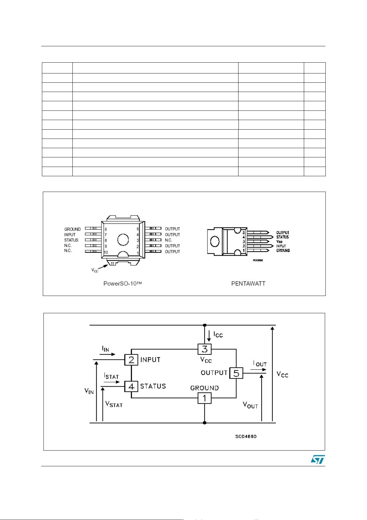
Figure 1. Connection Diagram (Top View)
Figure 2. Current and Voltage Conventions
2/13
Page 3
VN540-E / VN540SP-E / VN540-12-E
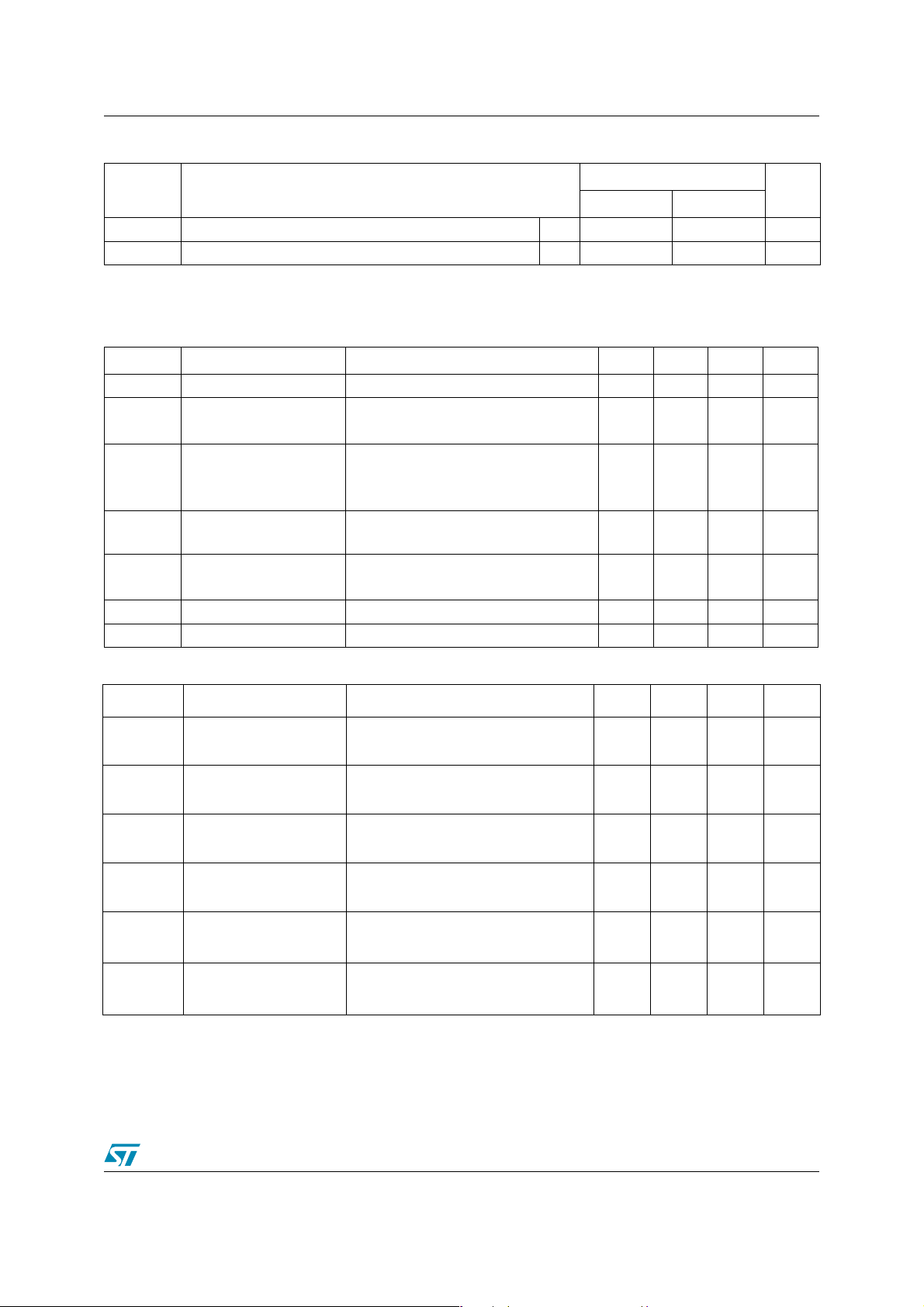
Table 2. Thermal data
Symbol Parameter
R
thJC
R
thJA
Thermal resistance junction-case Max 1.5 2.0 °C/W
Thermal resistance junction-ambient Max 50 60 °C/W
PowerSO-10 Pentawatt
Value
Unit
Electrical Chracteristics (10V < VCC < 36V; -25°C < TJ < 85°C; unles s ot herwise sp ec if ied)
Table 3. Power Section
Symbol Parameter T est Conditions Min. Typ. Max. Unit
V
R
I
I
LGND
V
V
demag
CC
ON
I
LS
Supply voltag e 10 36 V
= 2.8A; TJ = 25°C
I
On state resistance
OUT
I
OUT
= 2.8A;
OFF state
Supply current
S
Output leakage curr ent
Output current at turn-off
OL
Low state output voltage
Output voltage at turn-off
ON state; T
I
= 0A
OUT
Channel OFF
= 45V
V
CC
= VIN = V
V
CC
T
= - 25°C < TJ < 100°C
J
V
= V
IN
I
= 2.8A; L
OUT
= 125°C
J
GND
IL; RLOAD
LOAD
= V
STAT
= 24V
>= 10MΩ
>= 1mH VCC-65 VCC-55 VCC-45
50
90
1
3
mΩ
mΩ
mA
mA
100 µΑ
2mA
1.5 V
V
Table 4. Switching
Symbol Parameter Test Conditions Min. Typ. Max. Unit
I
t
d(ON)
t
d(OFF)
dI/dt
dI/dt
Turn-on delay on output
current
t
Rise time of output
r
current
Turn-off del ay time of
output current
t
Fall time of Output
f
current
Turn-on current average
(on)
slope
Turn-off current average
(off)
slope
= 2.8A, Resistive Load Input rise
OUT
time < 0.1µs, V
I
= 2.8A, Resistive Load Input rise
OUT
time < 0.1µs, V
I
= 2.8A, Resistive Load Input rise
OUT
time < 0.1µs, V
I
= 2.8A, Resistive Load Input rise
OUT
time < 0.1µs, V
I
= 2.8A,
OUT
I
= I
OUT
LIM
I
= 2.8A,
OUT
I
= I
OUT
LIM
= 24V; TJ = 25°C
CC
= 24V; TJ = 25°C
CC
= 24V; TJ = 25°C
CC
= 24V; TJ = 25°C
CC
; 25°C < TJ < 140°C
; 25°C < TJ < 140°C
40 µs
60 µs
60 µs
25 µs
0.5
2
2
4
Α/µs
Α/µs
3/13
Page 4
VN540-E / VN540SP- E / VN540-12-E
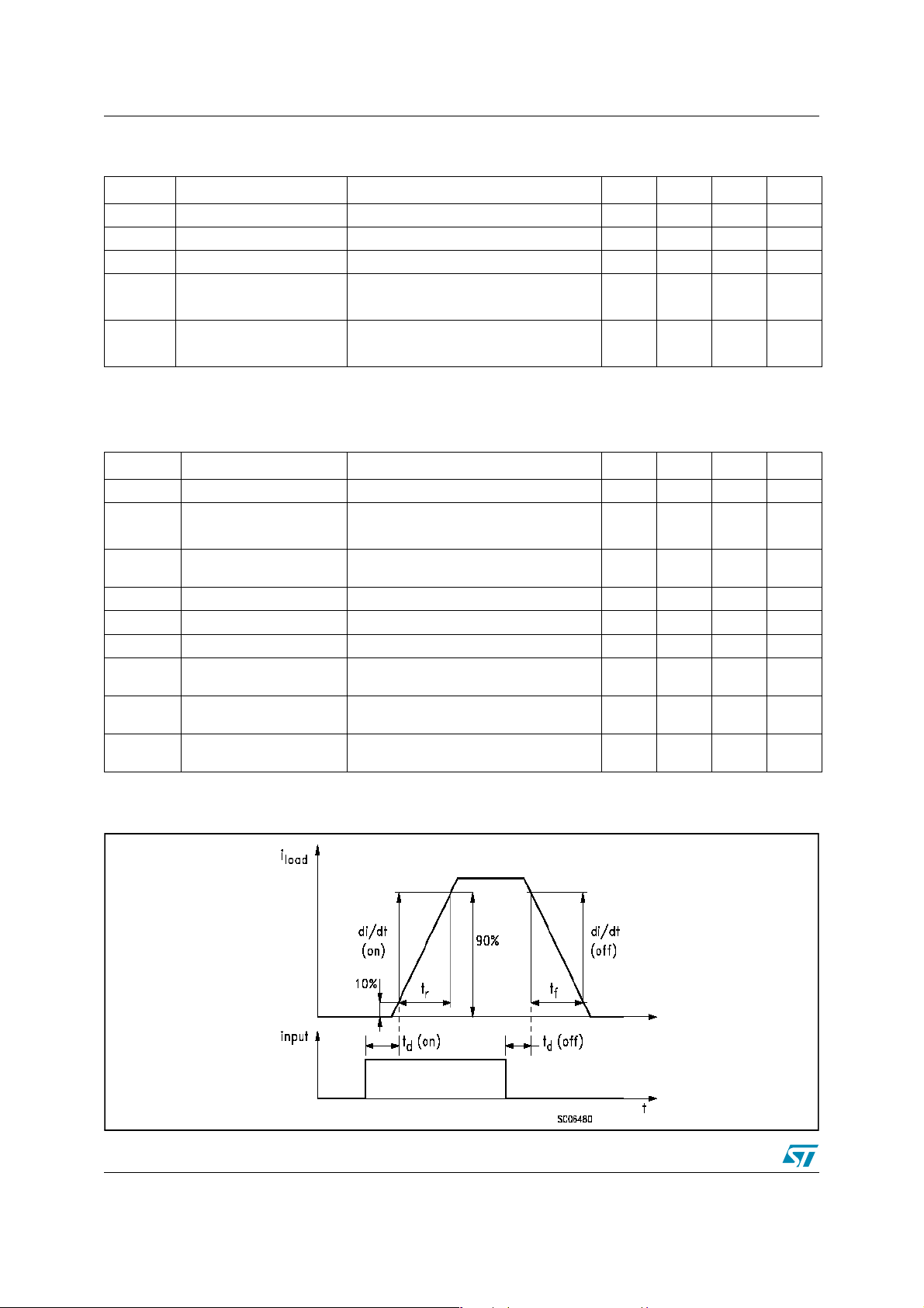
Table 5. Logical Input
Symbol Parameter Test Conditions Min. Typ. M ax. Unit
V
V
V
I(HYST)
I
V
Input low level vol tage 2.0 V
IL
Input high level vol tage 3.5 V
IH
Input hyster esis voltage 0.5 V
= 30V
V
Input current
IN
I/O Input clamp voltage
ICL
Note 1
IN
= 2.0V 25
V
IN
= 1mA
I
IN
= -1mA
I
IN
32 36
-0.7
300
µΑ
µΑ
V
V
Note: 1 The input voltage is internally clamped at 32V minimum, it is possible to connect the input pins
to an higher voltage via an external resistor calculate to not exeed 10mA
Table 6. Protection and Diagnostic
Symbol Para m eter Test Cond ition s Min. Typ. Max. Unit
V
V
SCL(*)
I
STAT
V
I
I
OVPK
T
STAT
USD
LIM
t
SC
TSD
T
R
Status output voltage
Status clamp voltage
Leakage on diagnostic
pin in high state
Undervoltage shut down 5.0 8.0 V
DC Short circuit current
Peak short circuit cur rent
Delay time of current
limiter
Thermal shut down
temperature
Thermal reset
temperature
= 5mA ( Fault condition )
I
STAT
= 1mA
I
STAT
= -1mA
I
STAT
V
= 5V
STAT
V
= 24V; R
CC
= 24V; VIN = 30; R
V
CC
LOAD
< 10mΩ
LOAD
< 10mΩ
1V
32 36
-0.7
V
V
10 µΑ
2.8 5.0 8.0 A
4A
100 µs
150 170 °C
135 155 °C
(*)Status determi nation > 100m s after the switching edge .
Figure 3. Switching Characteristics
4/13
Page 5
VN540-E / VN540SP-E / VN540-12-E
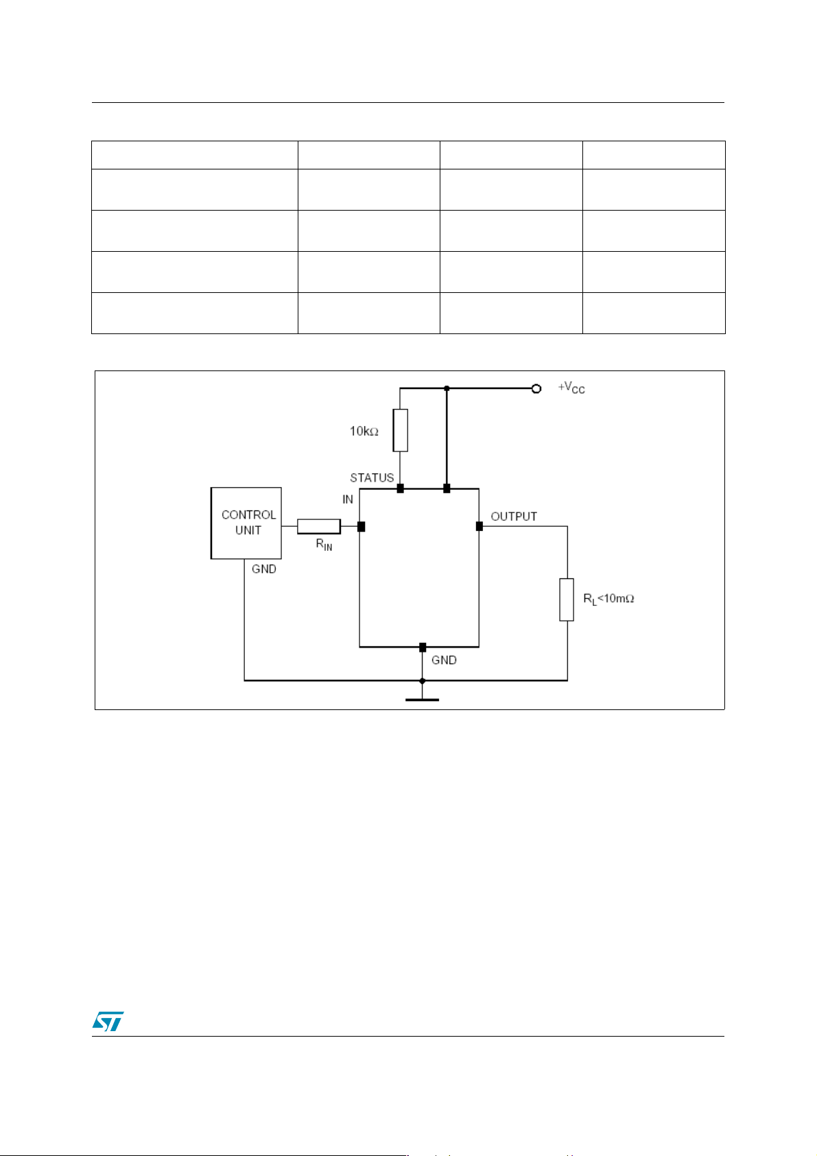
Table 7. Tru th Ta ble
INPUT OUTPUT STATUS
Normal operation
Overtemperature
Undervoltage
Shorted load
( Current limitati on )
Figure 4. Peak Short Test Circuit
L
H
L
H
L
H
L
H
L
H
L
L
L
L
L
H
H
H
H
L
H
H
H
H
5/13
Page 6
VN540-E / VN540SP- E / VN540-12-E
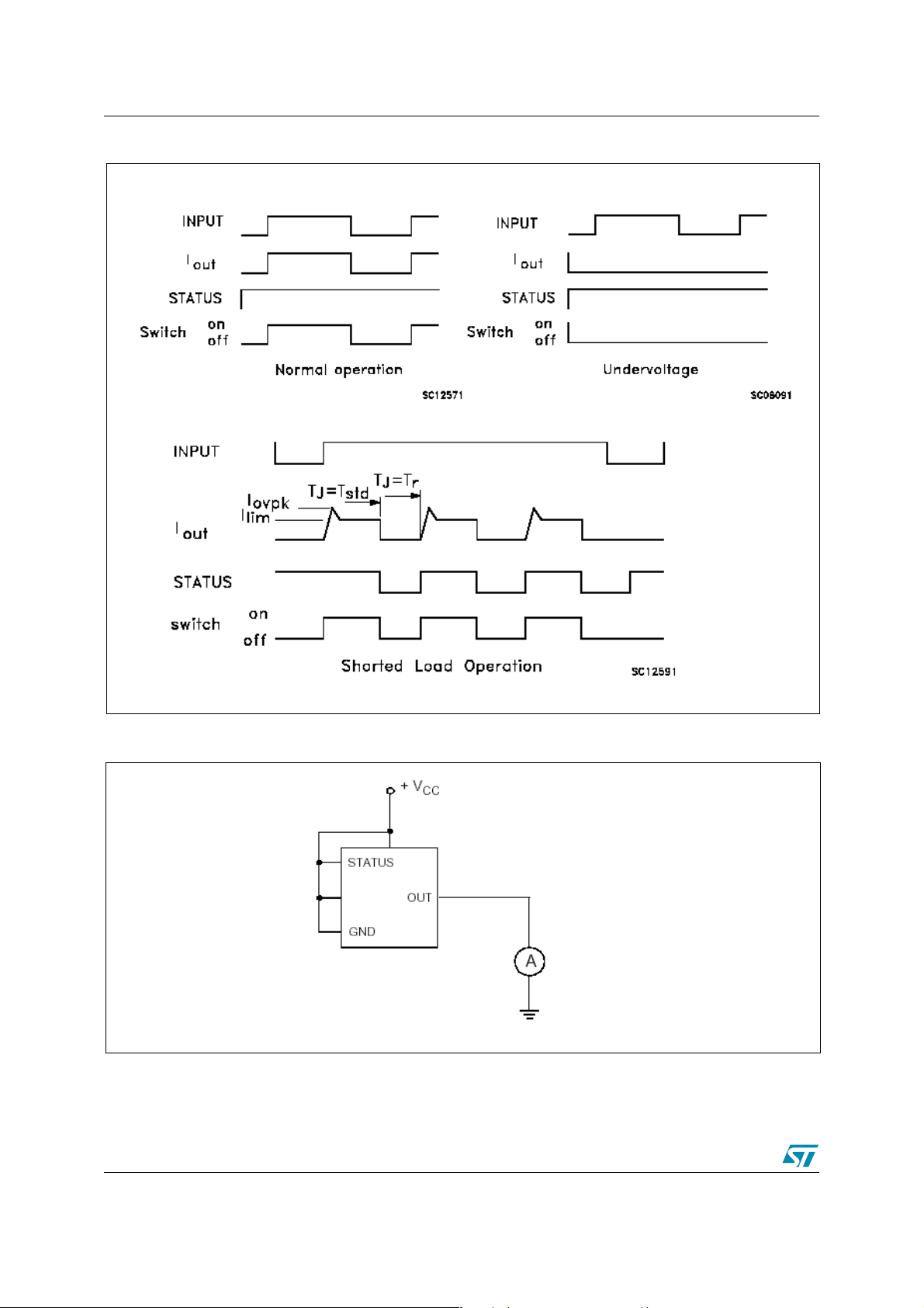
Figure 5. Switching Waveforms
Figure 6. I
Tes t Co nf ig uration
LGND
IN
6/13
Page 7

VN540-E / VN540SP-E / VN540-12-E
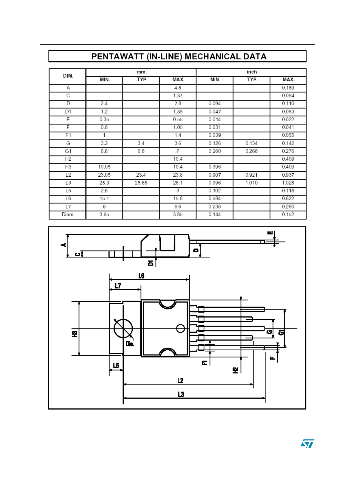
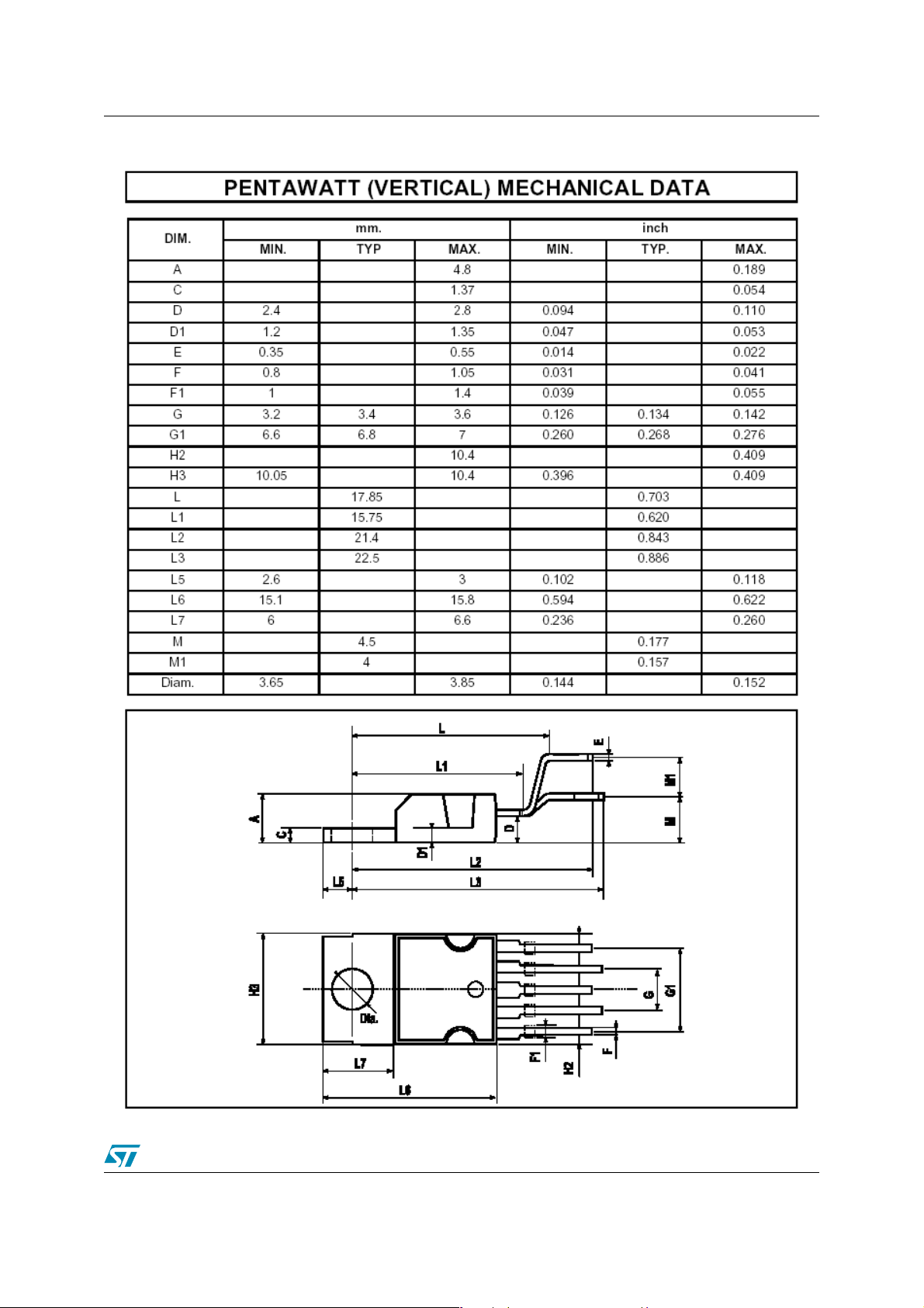
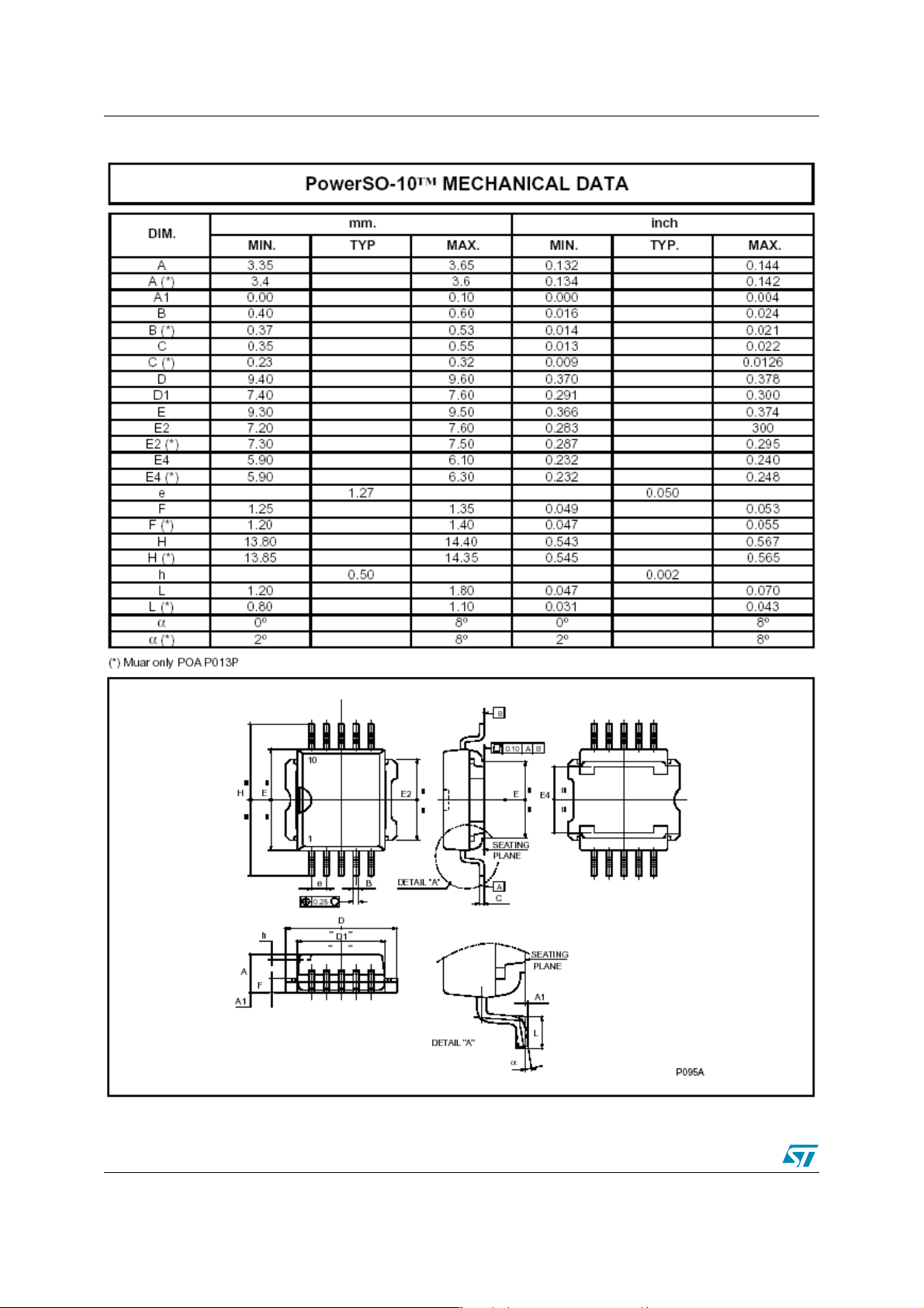
Package Mechanical Data
In order to meet environmental requirements, ST offers these devices in ECOPACK®
packages. These packages have a Lead-free second level interconnect. The catego ry of
second Level Interconnect is marked on the package and on the inner box label, in compliance
with JEDEC Standard JESD97. The maximum ratings related to soldering conditions are also
marked on the inner box label. ECOPACK is an ST trademark. ECOPACK specifications are
available at: www.st.com.
7/13
Page 8
VN540-E / VN540SP- E / VN540-12-E
8/13
Page 9
VN540-E / VN540SP-E / VN540-12-E
9/13
Page 10
VN540-E / VN540SP- E / VN540-12-E
10/13
Page 11
VN540-E / VN540SP-E / VN540-12-E
Table 8. Order Codes
Package T ube T ape and Reel
PowerSO-10
PENTAWATT vertical VN540-E
PENT AWATT straight VN540-12-E
TM
VN540SP-E VN540SPTR-E
11/13
Page 12
VN540-E / VN540SP- E / VN540-12-E
Table 9. Revision History
Date Revision Changes
2-Nov-2005 1 Initial release
12/13
Page 13

VN540-E / VN540SP-E / VN540-12-E
I
s
o
d
b
ct
t
ot
a
nformation furnished is believed to be accurate and reliable. However, STMicroelectronics assumes no responsibility for the consequence
f use of such information nor for any infringement of patents or other rights of third parties which may result from its use. No license is grante
y implic ation or otherwise u nder any pat ent or pat ent rights of STMicro el ectronics . Specificati ons menti oned in this publicati on are subje
o change without notice. This publication supersedes and replaces all information previously supplied. STMicroelectronics products are n
uthoriz ed for use as critical compo nents in life support devices or systems without express written approval of STMicroel ectronics.
The ST logo is a registered t rademark of ST M i croelectroni cs.
All other nam es are the pro perty of their respectiv e owners
© 2005 STMi croelectro ni cs - All rights reserved
Austra l i a - Be l gi um - Brazil - Canada - China - Czech Rep ubl i c - Finland - F rance - Germany - Hong Kon g - India - Israel - Italy - Japan -
Malaysi a - M al ta - Morocco - Singapore - Spain - Sweden - Switze rl and - Unite d Kingdom - Unit ed States of America
STMicroelectron ics group of com panies
www.st.com
13/13
 Loading...