

.
6 VIDEO INPUTS - 8VIDEO OUTPUTS
.
2 INTERNALSELECTABLEYC ADDERS
.
15MHz BANDWIDTH @ -3dB
.
SELECTABLE 0.5/6.5dB GAIN FOR EACH
OUTPUT
.
HIGH IMPEDANCE SWITCH FOR EACH
OUTPUT(3-stateoperation)
.
PROGRAMMABLE CLAMP MODE ON EACH
INPUT(sync bottom or average value)
.
-60dB CROSSTALK @ 5MHz
.
4 SUB-ADDRESSCAPABILITY
.
I2C BUS CONTROL
DESCRIPTION
Thisdeviceisintendedforswitchingbetweenvideo
and chroma signals such as CVBS,SVHS, baseband CVBS, MAC. Each input clamp mode, each
outputgain, all switchingare controlledthroughthe
2
Cbus.The8 outputscanbesetseparatelyinhigh
I
impedancestate, toenableparallelDC connection
of several devices (up to 4).
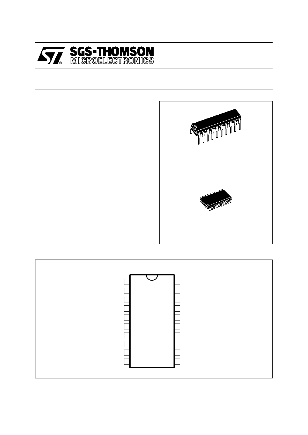
TEA6425
VIDEO CELLULAR MATRIX
DIP20
(Plastic Package)
ORDER CODE : TEA6425
SO20L
(Plastic Micropackage)
ORDER CODE : TEA6425D
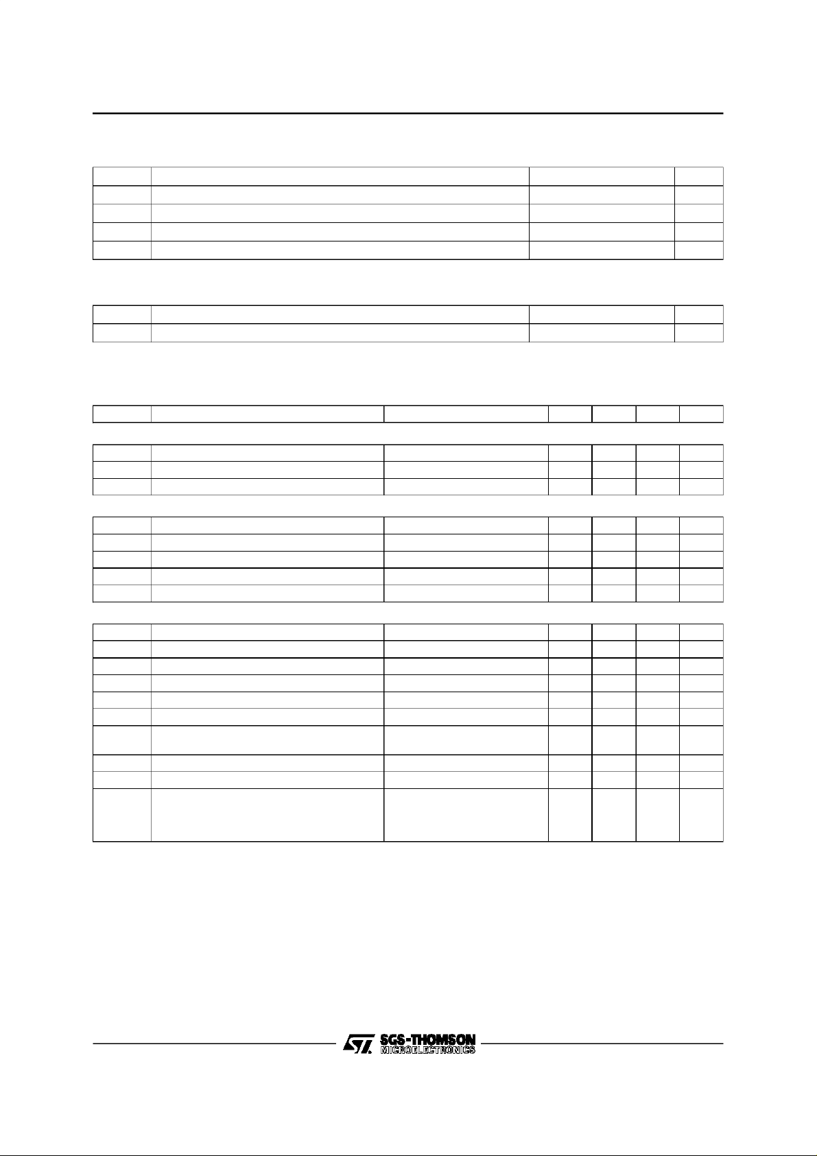
PINCONNECTIONS
May 1996
IN 1
SDA
IN 2
SCL
IN 3
IN 4
SUB
IN 5
V
CCP
IN 6
1
2
3
4
5
6
7
8
9
10
20
19
18
17
16
15
14
13
12
11
V
CC
OUT 1
OUT 2
OUT 3
OUT 4
OUT 5
OUT 6
OUT 7
OUT 8
GND
6425-01.EPS
1/9

TEA6425
BLOCK DIAGRAM
SUB-ADDRESS
INPUTS
SCL
SDA
V
CC1
V
CC2
1
3
5
6
8
10
4
2
7
9
20
TEA6425
PROG.
CLAMP
PROG.
CLAMP
PROG.
CLAMP
PROG.
CLAMP
PROG.
CLAMP
PROG.
CLAMP
I2C
DECODER
6x8
MATRIX
0/6dB0/6dB0/6dB0/6dB0/6dB0/6dB0/6dB0/6
3 S TATE OUTPUTS
11
GND
1312
OUTPUTS
dB
191817161514
6425-02.EPS
CELLULAR MATRICE CONNECTIONS
1st/4addresses
CVBS
or C
PROG.
CLAMP
2
IC
DECODER
6X8
Full MATRIX
IC1
ADDER
6 INPUTS
0dB
6dB
3STATE
OUT
8 OUTPUTS LINES
2nd/4 addresses
2
IC
DECODER
6X8
Full
MATRIX
IC2
6 INPUTS
IC3
IC4
6425-03.EPS
2/9
TEA6425
ABSOLUTEMAXIMUMRATINGS
Symbol Parameter Value Unit
V
V
T
oper
T
THERMALDATA
Supply Voltage 12 V
CC
Voltage at Pin i to GND 0, V
I
CC
Operating Ambient Temperature 0, + 70
Storage Temperature -20, + 150
stg
V
o
C
o
C
6425-01.TBL
Symbol Parameter Value Unit
R
th (j-a)
ELECTRICAL CHARACTERISTICS (VCC=8V,T
R
load
Junction-ambient Thermal Resistance Min. 80
=25oC, VIN= 1V, Gain = 6.5dB,C
amb
load
= 4.7kΩ ; Gain condition, clamp and 3-state are controlledby I2C bus, unless otherwisespecified)
=20pF,
o
Symbol Parameter Test Conditions Min. Typ. Max. Unit
SUPPLY
V
I
CC
SupplyVoltage 7.2 8 8.8 V
CC
SupplyCurrent 45 60 mA
RR SupplyVoltage Rejection f = 1kHz 40 46 dB
VIDEO INPUTS (clamping at bottom sync level)
V
V
V
I
clamp
clamp
I
Max. Signal Amplitude Clamp Active 2 V
IN
Clamp Level Clamp Active 1.7 2 2.3 V
InputDC Level Clamp Inactive 2.7 3 3.3 V
DC
Leakage Current 1 input connected to 1 output 2 5 µA
IN
Clamp Current V
- 200mV 0.9 3 mA
clamp
VIDEO OUTPUTS
R
OUT
Z
C
Output Resistance 15 50 Ω
Output ”off” Impedance no load 50 kΩ
HI
C
HI
in 3-state no load 3 pF
OUT
G1 Voltage Gain f = 100kHz 0 0.5 1 dB
G2 Voltage Gain f = 100kHz 6 6.5 7 dB
V
sync
V
Top Level Sync (Y or CVBS) G = 6.5dB, Clamp Active 1 1.25 2 V
Output Mean Level (chroma) G = 0.5dB, Clamp Inactive
bias
G = 6.5dB, Clamp Inactive
2
2.4
3
3.4
3
4
Isolation ”off” State f = 5MHz 60 dB
Crosstalk Attenuation between Channels f = 5MHz 50 60 dB
B Bandwidth C
= 20pF, G = 6.5dB
load
at ± 0.5dB
at ± 1dB
at - 3dB
5
10
21
C/W
PP
V
V
MHz
6425-02.TBL
6425-03.TBL
FUNCTIONAL DESCRIPTION
This device is controlled via the I2C bus. 4 addresses can be selected by a 4-level detector on
Pin 7, thus enabling parallel connection of 4 devices.
2
Viathe I
C bus :
- The input signals can be clampedat their negative peak(top sync).
- The gain factor of the outputs can be selected
between 0.5 and 6.5dB.
- Each of the 6 inputs can be connected to the 8
outputs.
- Each output can individually be set in a high
impedancestate.
Two internal SVHS mixerswill add the selectedY
and C inputs. Twodedicated outputswill have the
option to select this added signalalso.
3/9

TEA6425
I2C BUS CHARACTERISTICS
Symbol Parameter Test Conditions
SCL
Low Level Input Voltage - 0.3 +1.5 - 0.3 + 1.5 V
V
IL
V
High Level Input Voltage 3.0 VCC+ 0.5 3.0 VCC+ 0.5 V
IH
I
Input Leakage Current VI= 0 to V
LI
f
SCL
t
R
t
F
C
SDA
V
IL
V
IH
I
LI
C
t
R
t
F
V
OL
t
F
C
L
TIMING
t
LOW
t
HIGH
t
SU, DAT
t
HD,DAT
t
SU, STO
t
BUF
t
HD, STA
t
SU, STA
Clock Frequency 0 100 0 400 kHz
Input Rise Time 1.5V to 3V 1000 300 ns
Input Fall Time 1.5V to 3V 300 300 ns
Input Capacitance 10 10 pF
I
Low Level Input Voltage - 0.3 +1.5 - 0.3 + 1.5 V
High Level Input Voltage 3.0 VCC+ 0.5 3.0 VCC+ 0.5 V
Input Leakage Current VI= 0 to V
Input Capacitance 10 10 pF
I
Input Rise Time 1.5V to 3V 1000 300 ns
Input Fall Time 1.5V to 3V 300 300 ns
Low Level Output Voltage IOL= 3mA 0.4 0.4 V
Output Fall Time 3V to1.5V 250 250 ns
Load Capacitance 400 400 pF
Clock Low Period 4.7 1.3 µs
Clock High Period 4.0 0.6 µs
Data Set-upTime 250 100 ns
Data Hold Time 0 340 0 340 ns
Set-up Time from Clock High toStop 4.0 0.6 µs
Start Set-up Time following a Stop 4.7 1.3 µs
Start Hold Time 4.0 0.6 µs
Start Set-up Time following Clock Low-
to High Transition
DD
DD
Standard Mode Fast Mode
Min. Max. Min. Max.
Unit
- 10 + 10 - 10 + 10 µA
- 10 + 10 - 10 + 10 µA
4.7 0.6 µs
6425-04.TBL
Figure 1 : I2C Bus Timing
SDA
t
BUF
SCL
SDA
4/9
t
HD,STA
t
LOW
t
r
t
SU,STA t
t
HD,DAT
t
HIGH
t
f
t
SU,DAT
SU,STO
6425-04.EPS

TEA6425
I2C BUS SELECTION
2
I
C Bus Slave Address
Address A6 A5 A4 A3 A2 A1 A0 R/W
Value 10010A1A00
Sub-address I2C
Symbol Parameter Conditions Pin 7 Voltage (typ.) Unit
Vsub Slave address HEXA Sub-address
1
2
3
4
Note : The first 3 levelsare defined by connecting the sub-address pin to the appropriate level. Sub-address 4 will be selected
when this pin is left open.
90
96
94
92
1stData Byte
b7 b6 b5 b4 b3 b2 b1 b0
a2 a1 a0 * * * * I
0 0 0 * * * * 0 OUT1
0 0 1 * * * * 0 OUT2
Output
Select
0 1 0 * * * * 0 OUT3
0 1 1 * * * * 0 OUT4
1 0 0 * * * * 0 OUT5
1 0 1 * * * * 0 OUT6
1 1 0 * * * * 0 OUT7
1 1 1 * * * * 0 OUT8
(see note)
A1
0
1
1
0
A0
0
1
0
1
GND
V
CC
1/3
2/3
V
V
V
CC
V
CC
Selected
Output
2ndData Byte
Input
Select
Clamp
Gain
Mixer
Tri-state
b7 b6 b5 b4 b3 b2 b1 b0
a2 a1 a0 * * * * I
000****1 IN1
001****1 IN2
010****1 IN3
011****1 IN4
100****1 IN5
101****1 IN6
* * * 0 * * * 1 Free
* * * 1 * * * 1 Clamped
* * * * 0 * * 1 0.5dB
* * * * 1 * * 1 6.5dB
* * * * * 0 * 1 Disabled
* * * * * 1 * 1 Enabled
* * * * * * 0 1 Low impedance
* * * * * * 1 1 Tri-state
Action
Power On Reset
Whenactive : outputsin 3-state,inputs are clamped.
Symbol Parameter Conditions Min. Typ. Max. Unit
Reset Start of Reset
End of Reset
Incr. V
Decr. V
Incr. V
CC
CC
CC
2.5
4.2
4.5
V
V
V
5/9

TEA6425
PIN CONFIGURATIONS
Figure2 : Video IN
Figure3 : Video OUT
TRI-STATE
V
REF
Pins 1 - 3 - 5
6-8-10
TRI-STATE
Clamp
Clamp
TRI-STATE
to Matrix
V
REF
6425-05.EPS
From
Matrix
TRI-STATE
Figure 4 : PROG Pin
7
40kΩ 20kΩ
V
REF
TRISTATE
V
CC
V
REF
TRISTATE
to CM OS
Pins 12 - 13 - 14 - 15
16 - 17 - 18 - 19
TRISTATE TRISTATE
Figure5 : Bus Inputs
V
CC
Pins
2-4
X4
6425-06.EPS
ESD
PROT.
V
REF
to CMOS
6/9
3 TIMES IN //
6425-07.EPS
ACKN
For SDA only
6425-08.EPS

TYPICALAPPLICATION
SVHS1
SVHS2
SCART 1 (CVBS IN)
SCART 2 (CVBS IN)
SCART 3 (CVBS IN)
Y1
IN
C1
75
Y2
IN
C2
75
TUNEROUT
(CVBS)
2x
Ω
2x
Ω
3x
75Ω
TEA6425
V(+8V)
CC
22µF10µH
220nF
9
11
C1
1
C2
T
E
C3
C4
C5
C6
SDA
2
I
C
SCL
C7
C8
C9
C10
C11
C12
10
10
A
5
6
6
4
8
2
5
234
234
1
T
E
5
A
6
6
4
8
2
5
9
220nF
4.7kΩ 4.7kΩ
20
19
18
17
16
15
14
13
12
7
7
19
18
17
16
15
14
13
12
2011
75Ω
75
Ω
4.7kΩ
CVBS/Y
4.7k
Y
C
TOPIP PROCESSOR
(CVBSor Y+C)
TO TV PROCESSOR
C
(CVBS or YC)
75Ω
75Ω
75Ω
6x
Ω
EXT
SVHS OUT
SCART1
(CVBSOUT)
SCART2
(CVBSOUT)
SCART3
(CVBSOUT)
220nF
Y
COMB
FILTER
C
4.7kΩ
220nF
(CVBS)
SVHS 1/2
(Y+C)
6425-09.EPS
7/9

TEA6425
PACKAGE MECHANICAL DATA
20 PINS- PLASTICDIP
Dimensions
Min. Typ. Max. Min. Typ. Max.
a1 0.254 0.010
B 1.39 1.65 0.055 0.065
b 0.45 0.018
b1 0.25 0.010
D 25.4 1.000
E 8.5 0.335
e 2.54 0.100
e3 22.86 0.900
F 7.1 0.280
I 3.93 0.155
L 3.3 0.130
Z 1.34 0.053
Millimeters Inches
PM-DIP20.EPS
DIP20.TBL
8/9

PACKAGE MECHANICAL DATA
20 PINS- PLASTICMICROPACKAGE
Dimensions
Min. Typ. Max. Min. Typ. Max.
A 2.65 0.104
a1 0.1 0.3 0.004 0.012
a2 2.45 0.096
b 0.35 0.49 0.014 0.019
b1 0.23 0.32 0.009 0.013
C 0.5 0.020
c1 45
D 12.6 13.0 0.496 0.512
E 10 10.65 0.394 0.419
e 1.27 0.050
e3 11.43 0.450
F 7.4 7.6 0.291 0.299
L 0.5 1.27 0.020 0.050
M 0.75 0.030
S8
Millimeters Inches
o
(typ.)
o
(Max.)
TEA6425
PM-SO20.EPS
SO20.TBL
Information furnished is believed tobe accurate and reliable. However, SGS-THOMSON Microelectronics assumes no responsibility
for the consequences of use of suchinformation nor forany infringement ofpatents or other rights of third parties which may result
from its use. No licence is granted by implication or otherwiseunder any patent or patent rights ofSGS-THOMSON Microelectronics.
Specifications mentioned in this publication are subject to change without notice. This publication supersedes and replaces all
information previously supplied.SGS-THOMSON Microelectronics products are not authorized for useas critical components in life
support devices or systems withoutexpress written approval of SGS-THOMSON Microelectronics.
1996 SGS-THOMSON Microelectronics - All Rights Reserved
Purchase of I
2
I
C Patent. Rights to usethese components in a I2C system,is granted provided that the system conforms to
Australia - Brazil - Canada - China - France - Germany -Hong Kong - Italy- Japan - Korea - Malaysia - Malta- Morocco
The Netherlands - Singapore -Spain - Sweden - Switzerland - Taiwan - Thailand - United Kingdom - U.S.A.
2
C Components of SGS-THOMSON Microelectronics,conveys a license under the Philips
2
the I
C Standard Specifications as defined by Philips.
SGS-THOMSON Microelectronics GROUP OF COMPANIES
9/9
 Loading...