

Page 1
TELEFUNKEN Semiconductors
TV Vertical Deflection Output Amplifier
Technology: Bipolar
Features
D
Output peak current, I5 = 2 A
D
Flyback current, peak to peak, I3 = 3 A
Case: 7 leads special plastic case
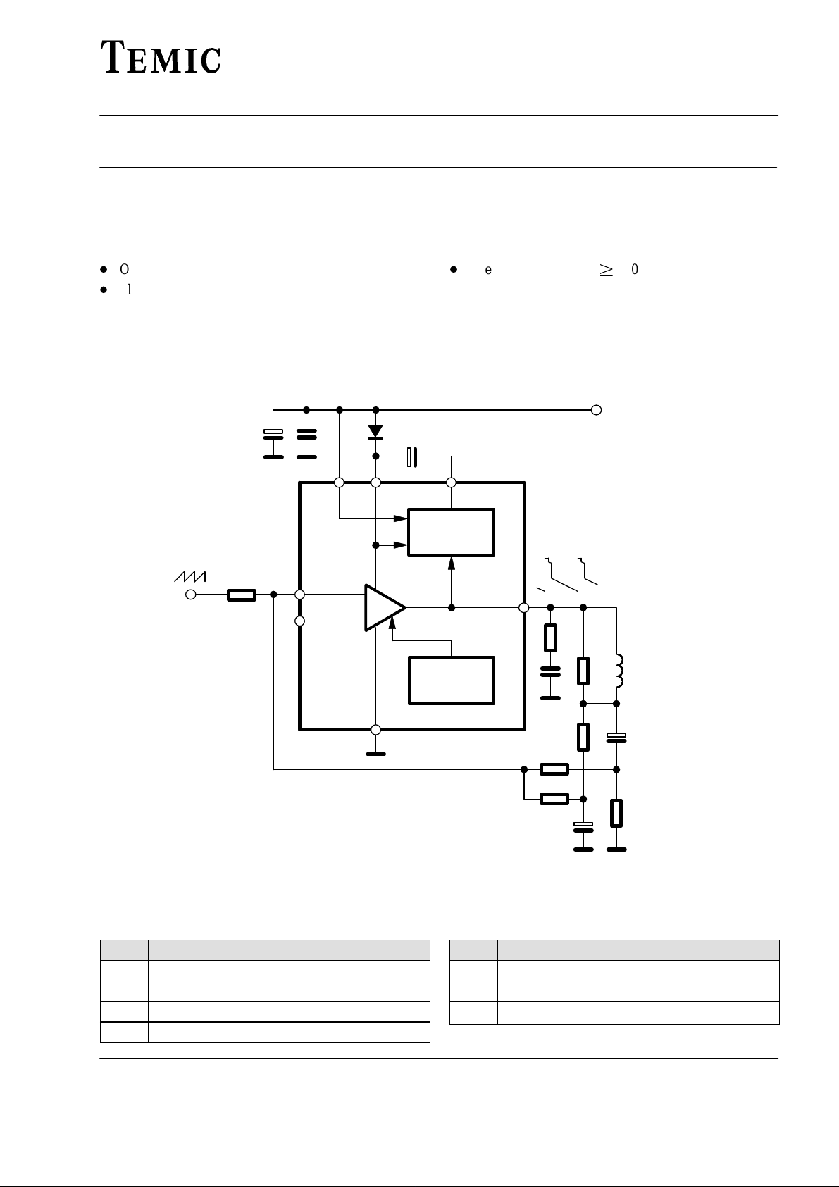
Block diagram
6
23
D
Thermal protection, Tj 140°C
+ V
TEA 8172
S
94 8723
Pin Configuration
1
Power
amplifier
–
7
+
4
Figure 1 Block diagram
Flyback
generator
Thermal
protection
5
Deflection
coil
Pin Function
1 Inverted input
2 Supply voltage
3 Flyback generator
4 Ground
Rev . A1: 17.07.1995
Pin Function
5 Output
6 Output stage supply
7
Non inverted input
1
Page 2
TEA 8172
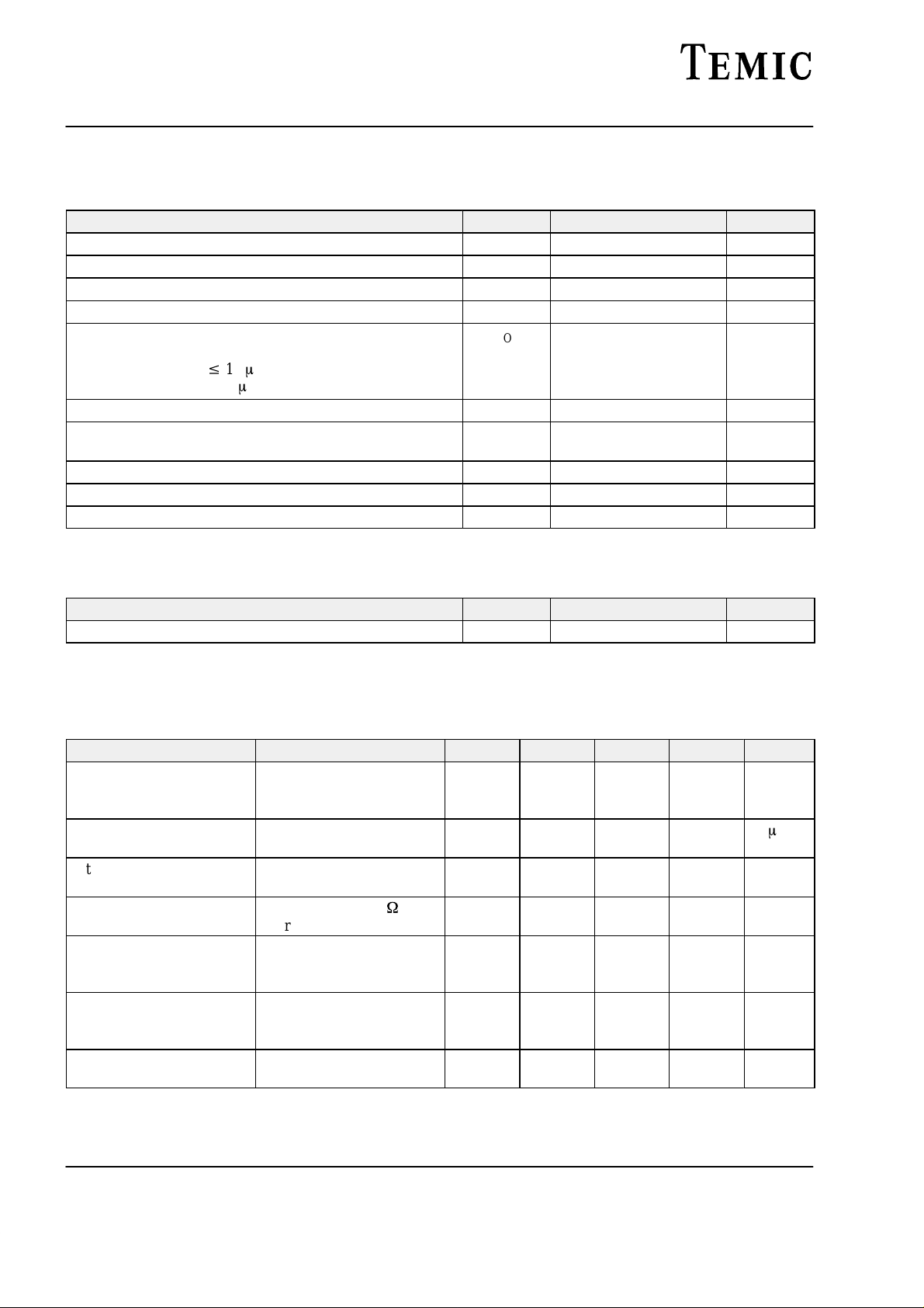
Absolute Maximum Ratings
Parameters Symbol Value Unit
Supply voltage Pin 2 V
Flyback peak voltage Pins 5 and 6 V
Voltage at pin 3 V
Input voltage Pins 1 and 7 V
Output peak current: Pin 5
t = 2 ms, non repetitive
f = 50/60 Hz, t v10 ms
f = 50/60 Hz, t > 10 ms
DC current at pin 3, V
Flyback current peak to peak, Pin 3
f= 50/60 Hz, t
Power dissipation, T
Storage temperature T
Junction temperature T
V
5 <
2
≤ 1.5 ms
fly
= 70°C P
case
I
I
I
S
5, 6
3
1, 7
O
3
3
tot
stg
j
TELEFUNKEN Semiconductors
35 V
60 V
V
S
V
S
2.5
3.0
2.0
100 mA
3 A
20 W
– 40 to + 150 °C
– 40 to + 150 °C
V
V
A
Thermal Resistance
Parameters Symbol Maximum Unit
Junction case R
Electrical Characteristics
V
= 35 V, T
S
Quiescent current I3 = 0, I
Input quiescent current V
Saturation voltage to GND I
Output voltage V
Saturation voltage to GND I5 = 0.7 A Pin 5
Saturation voltage to
supply
Junction temperature for
thermal shut down
= 25°C, reference point Pin 4 (GND), see test circuits, unless otherwise specified
amb
Parameters Test Conditions / Pin Symbol Min Typ Max Unit
I
= 0, I
3
0 Pin 2
S =
0 Pin 6
S =
I
I
figure 2
= 1 V Pin 1
1
–I
figure 3
= 20 mA Pin 3
3
V
figure 4
= 35 V, R
S
= 39 k
r
W
V
figure 5 Pin 5
V
I
= 1.2 A
5
figure 6
I5 = – 0.7 A Pin 5
I
= – 1.2 A
5
V
figure 7
T
2
6
3-4
5-4
5-6
thJC
1
3 K/W
8
16
16
36
0.1 1
mA
m
A
1 1.5 V
5
j
18 V
0.7
1.0
1.3
1.6
1.0
1.4
1.8
2.2
V
V
140 °C
2
Rev . A1: 17.07.1995
Page 3
TELEFUNKEN Semiconductors
I
2
2
I
6
6
TEA 8172
+V
S
+V
5
2
6
S
94 8726
3 V
W
10 k
1
7
V
7
4
94 8725
94 8724
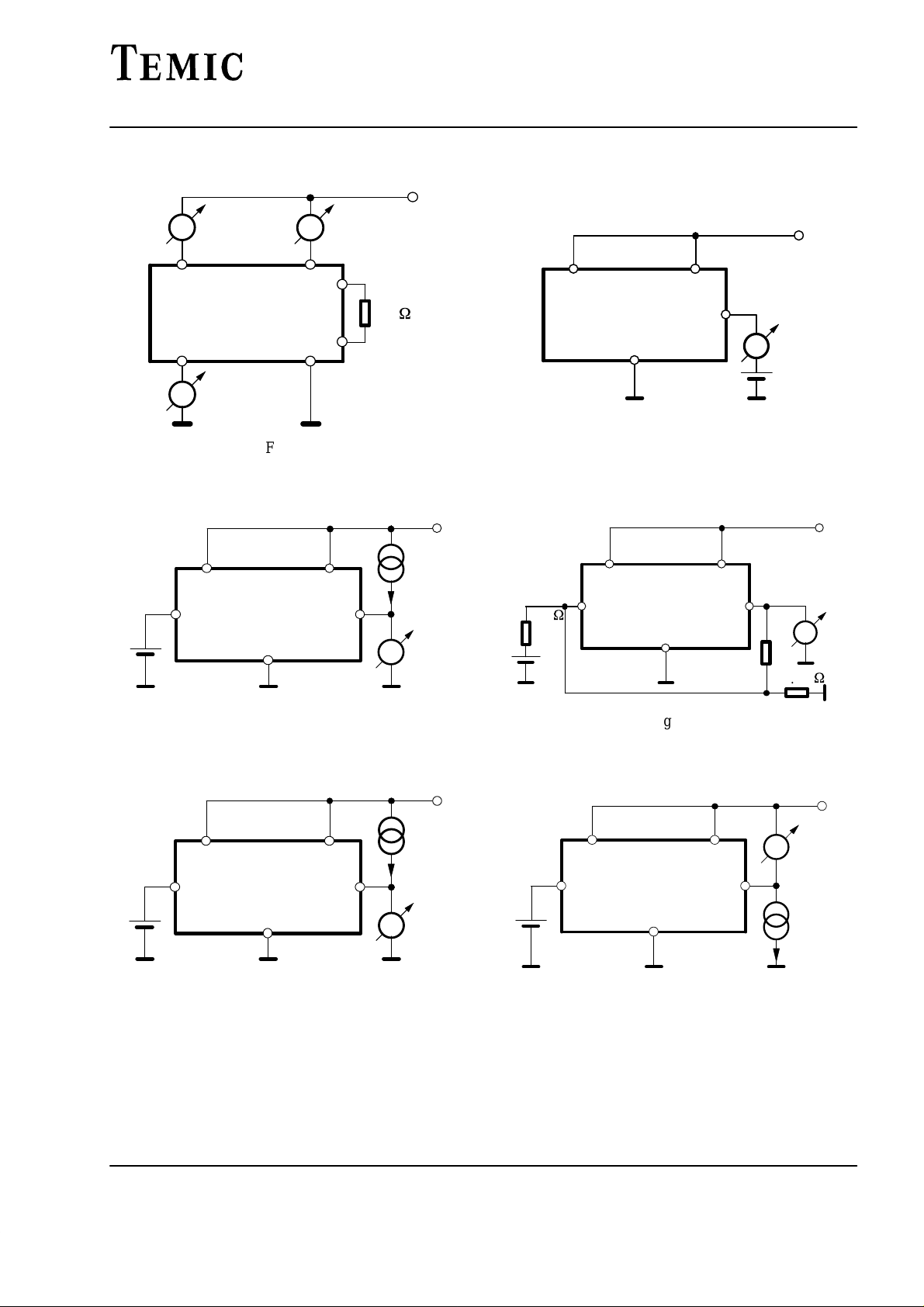
Figure 2
94 8727
+V
2
1
6
3
4
S
I
3
V
3–4
12 k
2 V
1
W
Figure 4
4
Figure 3
2
4
Figure 5
1
I
1
1 V
+V
r
5.6 k
S
V
5
W
6
5
R
94 8728
2
1
3 V
Rev . A1: 17.07.1995
4
Figure 6
94 8729
+V
6
5
S
I
5
V
5–4
1 V
2
1
6
5
4
+V
S
V
5–6
I
5
Figure 7
3
Page 4
TEA 8172
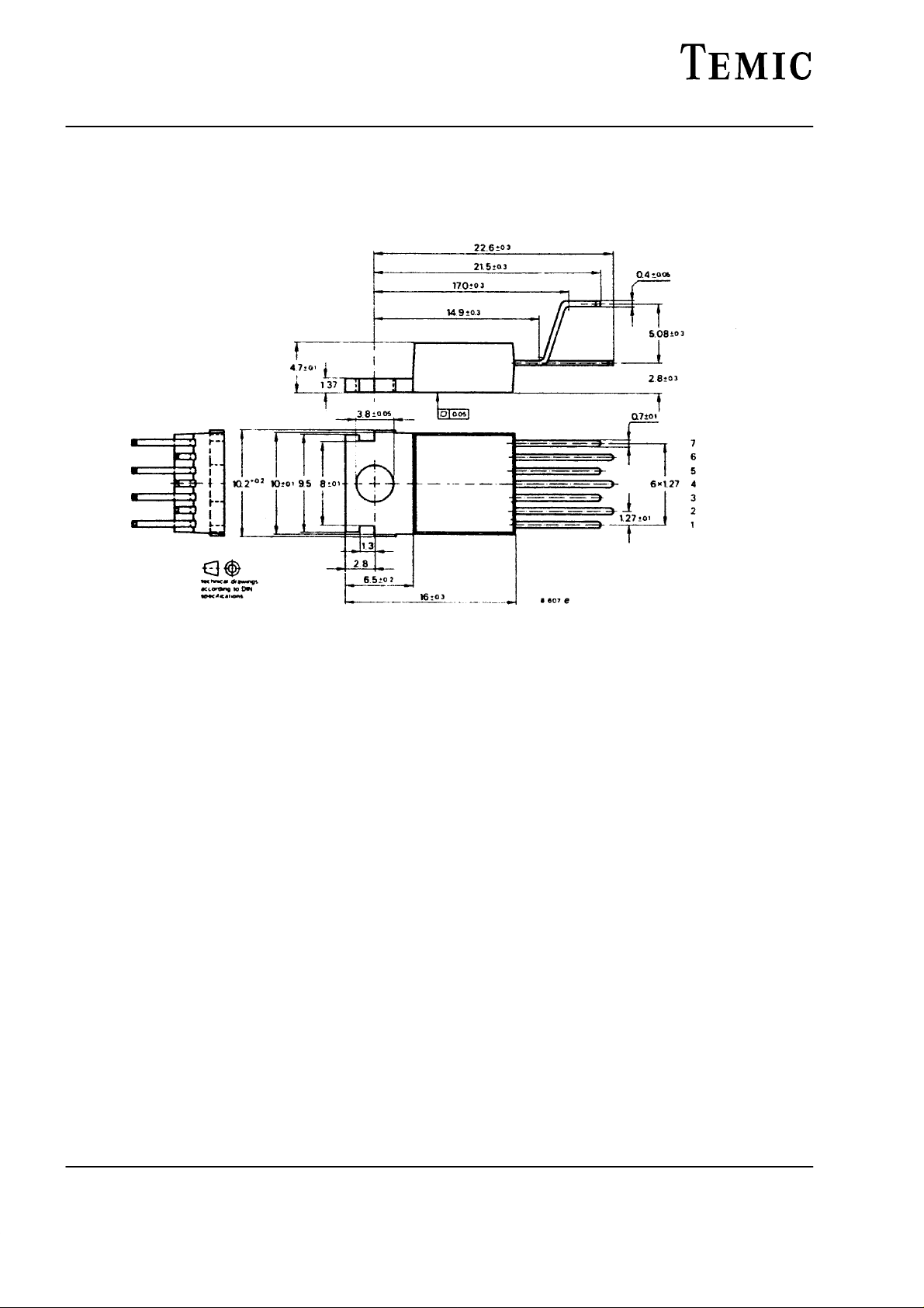
Dimensions in mm
7 leads special plastic case
TELEFUNKEN Semiconductors
We reserve the right to make changes without further notice to improve technical design.
Parameters can vary in different applications. All operating parameters must be validated for each customer
application by customer. Should Buyer use TEMIC products for any unintended or unauthorized application, Buyer
shall indemnify TEMIC against all claims, costs, damages, and expenses, arising out of, directly or indirectly, any
claim of personal damage, injury or death associated with such unintended or unauthorized use.
TEMIC TELEFUNKEN microelectronic GmbH, P.O.B. 3535, D-74025 Heilbronn, Germany
Telephone: 49 (0)7131 67 2831, Fax Number: 49 (0)7131 67 2423
4
Rev . A1: 17.07.1995
 Loading...