

Page 1

INTEGRATED CIRCUITS
DATA SH EET
TEA6840H
New In Car Entertainment (NICE)
car radio
Product specification
Supersedes data of 1999 Jul 12
File under Integrated Circuits, IC01
2001 Mar 08
Page 2

Philips Semiconductors Product specification
New In Car Entertainment (NICE) car radio TEA6840H
CONTENTS
1 FEATURES
2 GENERAL DESCRIPTION
3 QUICK REFERENCE DATA
4 ORDERING INFORMATION
5 BLOCK DIAGRAM
6 PINNING
7 FUNCTIONAL DESCRIPTION
7.1 Oscillators
7.1.1 VCO
7.1.2 Crystal oscillator
7.1.3 PLL
7.2 FM signal channel
7.2.1 DAA
7.2.2 FM I/Q mixer
7.2.3 FM keyed AGC
7.2.4 FM IF amplifiers
7.2.5 FM demodulator
7.3 AM signal channel
7.3.1 AM tuner including mixer 1 and mixer 2
7.3.2 AM RF AGC and IF2 AGC
7.3.3 AM detector
7.3.4 AM AF or IF2 switch
7.3.5 AM noise detector and blanker
7.3.6 FM and AM level detector
7.4 Test mode
8 LIMITING VALUES
9 THERMAL CHARACTERISTICS
10 DC CHARACTERISTICS
11 AC CHARACTERISTICS
12 I2C-BUS PROTOCOL
12.1 I2C-bus specification
12.1.1 Test mode
12.1.2 Data transfer for the TEA6840H
12.1.3 I2C-bus pull-up resistors
12.1.4 Frequency setting
12.2 I2C-bus protocol
12.2.1 Data transfer mode and IC address
12.2.2 Write mode: data byte 1
12.2.3 Write mode: data byte 2
12.2.4 Write mode: data byte 3
12.2.5 Write mode: data byte 4
12.2.6 Write mode: data byte 5
12.2.7 Write mode: data byte 6
12.2.8 Read mode: data byte 1
13 TEST AND APPLICATION INFORMATION
14 PACKAGE OUTLINE
15 SOLDERING
15.1 Introduction to soldering surface mount
packages
15.2 Reflow soldering
15.3 Wave soldering
15.4 Manual soldering
15.5 Suitability of surface mount IC packages for
wave and reflow soldering methods
16 DATA SHEET STATUS
17 DEFINITIONS
18 DISCLAIMERS
19 PURCHASE OF PHILIPS I2C COMPONENTS
2001 Mar 08 2
Page 3

Philips Semiconductors Product specification
New In Car Entertainment (NICE) car radio TEA6840H
1 FEATURES
• FM mixer for conversion of FM RF from 65 to 108 MHz
to IF of 10.7 MHz; the mixer provides inherent image
rejection
• FM RF mixer can be set to receive weather band radio
up to 162.55 MHz; weather band radio flag output
• AM mixer 1 for conversion of AM RF to AM IF1 of
10.7 MHz
• LC tuner oscillator providing mixer frequencies for
FM mixer and AM mixer 1
• AM mixer 2 for conversion of AM IF1 to AM IF2 of
450 kHz
• Crystal oscillator providing mixer frequencies for
AM mixer 2andreferenceforsynthesizerPLL,IF count,
timing for Radio Data System (RDS) update and
reference frequency for car audio signal processor ICs
• FastsynthesizerPLLtuning system with local control for
inaudible RDS updating
• Timing function for RDS update algorithm and control
signal output for car audio signal processor ICs
(TEA688x, SAA77xx) or car radio integrated signal
processor IC (TEF6890H)
• Digital auto alignment circuit for conversion of
LC oscillator tuning voltage to controlled alignment
voltage of FM antenna tank circuit
• AGC PIN diode drive circuit for FM RF AGC; AGC
detection at FM mixer input; the AGC PIN diode drive
can be activated by the I2C-bus as a local or distance
function; AGC threshold is a programmable and keyed
function switchable via the I2C-bus
• FM IF linear amplifiers with high dynamic input range
• FM quadrature demodulator with automatic centre
frequency adjustment and Total Harmonic Distortion
(THD) compensation
• Level detector for AM and FM with temperature
compensated output voltage; starting point and slope of
level output is programmable via the I2C-bus
• AM RF PIN diode drive circuit; AGC threshold detection
at AM mixer 1 and IF2 AGC input; threshold is
programmable via the I2C-bus; AM IF2 AGC and
demodulator
• AM AF output switchable to provide AM IF2 for
AM stereo decoder
• AM noise blanker with blanking at AM IF2
• Several test modes available for fast IC and system
tests.
2 GENERAL DESCRIPTION
The TEA6840H is a single IC with car radio tuner for
AM and FM intended for microcontroller tuning with the
I2C-bus providing the following functions:
• AM double conversion receiver for LW, MW and SW
(31 m, 41 m and 49 m bands) with IF1 = 10.7 MHz and
IF2 = 450 kHz
• FM single conversion receiver with integrated image
rejection for IF = 10.7 MHz capable of selecting US FM,
US weather, Europe FM, East Europe FM and Japan
FM bands.
2001 Mar 08 3
Page 4

Philips Semiconductors Product specification
New In Car Entertainment (NICE) car radio TEA6840H
3 QUICK REFERENCE DATA
SYMBOL PARAMETER CONDITIONS MIN. TYP. MAX. UNIT
V
DDA(n)
I
DDA(tot)
V
DDA2
I
DDA2
V
DDD
I
DDD
f
AM(ant)
f
FM(ant)
f
FM(WB)(ant)
T
amb
AM overall system parameters (1 × SFE10.7MS3; 1 × SFR450H)
(S+N)/N signal plus noise-to-noise ratio m = 0.3 − 58 − dB
THD total harmonic distortion m = 0.8 − 0.3 − %
FM overall system parameters (3 × SFE10.7MS3)
(S+N)/N signal plus noise-to-noise ratio ∆f = 22.5 kHz;
THD total harmonic distortion ∆f=75kHz − 0.6 1 %
analog supply voltage 1, 3, 4, 5
8 8.5 9 V
and 6
total analog supply current 1, 3, 4,
5 and 6
FM mode 45 56 67 mA
AM mode 39 49 59 mA
analog supply voltage 2 4.75 5 5.25 V
analog supply current 2 FM mode 6.5 8.1 9.8 mA
AM mode 4.7 5.9 7.1 mA
digital supply voltage 4.75 5 5.25 V
digital supply current FM mode 18 23 28 mA
AM mode 18 23 28 mA
AM input frequency LW 0.144 − 0.288 MHz
MW 0.522 − 1.710 MHz
SW 5.85 − 9.99 MHz
FM input frequency 65 − 108 MHz
FM weather band input frequency 162.4 − 162.55 MHz
ambient temperature −40 − +85 °C
m = 0.9 − 0.5 − %
− 65 − dB
de-emphasis = 50 µs
4 ORDERING INFORMATION
TYPE
NUMBER
NAME DESCRIPTION VERSION
PACKAGE
TEA6840H QFP64 plastic quad flat package; 64 leads (lead length 1.95 mm);
body 14 × 20 × 2.8 mm
2001 Mar 08 4
SOT319-2
Page 5

This text is here in white to force landscape pages to be rotated correctly when browsing through the pdf in the Acrobat reader.This text is here in
_white to force landscape pages to be rotated correctly when browsing through the pdf in the Acrobat reader.This text is here inThis text is here in
white to force landscape pages to be rotated correctly when browsing through the pdf in the Acrobat reader. white to force landscape pages to be ...
2001 Mar 08 5
5 BLOCK DIAGRAM
Philips Semiconductors Product specification
New In Car Entertainment (NICE) car radio TEA6840H
DAATD
DAAOUT
T1FMAGC
T2FMAGC
IFMAGC
FMMIXIN1
RFGND
FMMIXIN2
V
ref(FMMIX)
IAMAGC
T2AMAGC
T1AMAGC
VCO
BLANK
PULSE
V
10
DDA3
93456278
SEQUENTIAL
CIRCUIT FOR
RDS UPDATING
I2C-bus
×
AM
MIXER2
AM
IF AGC
AM
LEVEL
AMAFIF2AFHOLD
AM
DETECTOR
FM IF
AM IF2
LEVEL
DAA
LIMITER/
LEVEL
Σ
FM
FMMPXRDSMPXTRDSMUTEAFSAMPLEOSCTNKVCOGND
MUTE
IF
COUNT
V
DDA2
2 ms/20 ms
DEMODULATOR
CRYSTAL
OSCILLATOR
V
POWER
SUPPLY
I2C-BUS
DDA1
1
64
63
62
61
60
59
58
57
56
55
54
SDA
SCL
IF2GND
QDET2
QDET1
C
AFC
V
level
XTAL2
XTALGND
XTAL1
I
ref
V
DDD
10.25 MHz
DGND
TEA6840H
PEAK/
AVERAGE
CPOUTDAAIN
TUNING SYSTEM
V
DDA4
16 1314151718
WX
N1
÷2
90°
AM-NOISE
DETECTOR
N2
÷5/10
ref
V
tune
19
20
ANTENNA
21
22
23
24
25
26
27
28
29
30
31
AGC
AM
RF AGC
FM
DAA
AM
×
FM
I/Q MIXER
90°
f
OSCFDB
12 11
AMMIX1IN1
32
AM
MIXER 1
33 34
AMMIX1IN2
×
35 36
MIX1OUT1 IFAMP1DEC IFAMP1IN IFAMP1OUT IF1GND FMLIMIN
V
DDA5
MIX1OUT2
37 38 39
V
DDA6
IFAMP1
40 41 42 4543 44 46 50494847
IFAMP2DEC IFAMP2IN AMIF2IN AMIF2DEC
Fig.1 Block diagram.
C
handbook, full pagewidth
offset
IFAMP2
AMNBHOLD
IFAMP2OUT
C
FMLIMDEC
51
AGC
53
52
MGU326
AMMIX2OUT2
AMMIX2OUT1
Page 6

Philips Semiconductors Product specification
New In Car Entertainment (NICE) car radio TEA6840H
6 PINNING
SYMBOL PIN DESCRIPTION
V
DDA1
V
DDA2
FMMPX 3 FM demodulator MPX output
RDSMPX 4 MPX output for RDS decoder and signal processor (not muted)
AMAFIF2 5 AM demodulator AF output or IF2 output for AM stereo (multiplexed by I2C-bus)
TRDSMUTE 6 time constant for RDS update mute
AFHOLD 7 AF hold flag output for car audio signal processor IC
AFSAMPLE 8 AF sample flag output for car audio signal processor IC
V
DDA3
OSCTNK 10 VCO tank circuit
OSCFDB 11 VCO feedback
VCOGND 12 VCO ground
DGND 13 digital ground
V
DDD
f
ref
V
DDA4
CPOUT 17 charge pump output
V
tune
DAAIN 19 input of digital auto alignment circuit for antenna tank circuit
DAATD 20 temperature compensation diode of digital auto alignment circuit for antenna tank circuit
DAAOUT 21 output of digital auto alignment circuit for antenna tank circuit
T1FMAGC 22 1st time constant of FM front-end AGC
T2FMAGC 23 2nd time constant of FM front-end AGC
IFMAGC 24 PIN diode drive current output of FM front-end AGC
FMMIXIN1 25 FM RF mixer input 1
RFGND 26 RF ground
FMMIXIN2 27 FM RF mixer input 2
V
ref(FMMIX)
IAMAGC 29 PIN diode drive current output of AM front-end AGC
T2AMAGC 30 2nd time constant of AM front-end AGC
T1AMAGC 31 1st time constant of AM front-end AGC
AMMIX1IN1 32 AM mixer 1 input 1
AMMIX1IN2 33 AM mixer 1 input 2
V
DDA5
MIX1OUT1 35 FM mixer and AM mixer 1 IF output 1 (10.7 MHz)
MIX1OUT2 36 FM mixer and AM mixer 1 IF output 2 (10.7 MHz)
IFAMP1DEC 37 AM mixer 2 and FM IF amplifier 1 decoupling
V
DDA6
IFAMP1IN 39 IF amplifier 1 and AM mixer 2 input (10.7 MHz)
IFAMP1OUT 40 IF amplifier 1 output (10.7 MHz)
1 analog supply voltage 1 (8.5 V) for on-chip power supply
2 analog supply voltage 2 (5 V) for on-chip power supply
9 analog supply voltage 3 (8.5 V) for VCO
14 digital supply voltage (5 V)
15 reference frequency output for signal processor IC
16 analog supply voltage 4 (8.5 V) for tuning PLL
18 tuning voltage
28 reference voltage for FM I/Q mixer
34 analog supply voltage 5 (8.5 V) for FM mixer and AM mixer 1
38 analog supply voltage 6 (8.5 V) for IF amplifier 1 and 2
2001 Mar 08 6
Page 7

Philips Semiconductors Product specification
New In Car Entertainment (NICE) car radio TEA6840H
SYMBOL PIN DESCRIPTION
IFAMP2DEC 41 IF amplifier 2 decoupling and AGC capacitor for AM noise blanker
C
offset
IFAMP2IN 43 IF amplifier 2 input (10.7 MHz)
IF1GND 44 AM IF1 ground
AMIF2IN 45 AM IF2 input (450 kHz) for demodulator AGC and AM level detector
AMNBHOLD 46 AM noise blanker threshold
IFAMP2OUT 47 IF amplifier 2 output (10.7 MHz)
AMIF2DEC 48 decoupling for AM IF2 input
FMLIMIN 49 FM limiter input (10.7 MHz)
FMLIMDEC 50 FM limiter decoupling
C
AGC
AMMIX2OUT1 52 AM mixer 2 output 1 (450 kHz)
AMMIX2OUT2 53 AM mixer 2 output 2 (450 kHz)
I
ref
XTAL1 55 crystal oscillator 1
XTALGND 56 crystal oscillator ground
XTAL2 57 crystal oscillator 2
V
level
C
AFC
QDET1 60 quadrature demodulator tank 1
QDET2 61 quadrature demodulator tank 2
IF2GND 62 AM IF2 ground
SCL 63 I2C-bus clock line input
SDA 64 I2C-bus data line input and output
42 DC feedback for offset compensation RDS mute
51 AM IF AGC capacitor
54 reference current for power supply
58 level voltage output for AM and FM
59 FM demodulator AFC capacitor
2001 Mar 08 7
Page 8

Philips Semiconductors Product specification
New In Car Entertainment (NICE) car radio TEA6840H
handbook, full pagewidth
AFC
V
DDA1
V
DDA2
FMMPX
SCL
IF2GND
SDA
64
63
1
2
3
QDET2
QDET1
62
61
60
level
XTAL2
57
XTALGND
56
V
C
59
58
XTAL1
55
ref
I
AMMIX2OUT2
54
53
AMMIX2OUT1
52
C
51
AGC
FMLIMDEC
50
FMLIMIN
49
RDSMPX
AMAFIF2
TRDSMUTE
AFHOLD
AFSAMPLE
V
DDA3
OSCTNK
OSCFDB
VCOGND
DGND
V
DDD
f
ref
V
DDA4
CPOUT
V
tune
DAAIN
4
5
6
7
8
9
23
24
IFMAGC
T2FMAGC
TEA6840H
25
26
RFGND
FMMIXIN1
27
28
FMMIXIN2
ref(FMMIX)
V
29
30
IFMAGC
T2AMAGC
31
T1AMAGC
10
11
12
13
14
15
16
17
18
19
20
21
22
DAATD
DAAOUT
T1FMAGC
AMIF2DEC
48
IFAMP2OUT
47
AMNBHOLD
46
AMIF2IN
45
IF1GND
44
IFAMP2IN
43
C
42
IFAMP2DEC
41
IFAMP1OUT
40
IFAMP1IN
39
V
38
IFAMP1DEC
37
MIX1OUT2
36
MIX1OUT1
35
V
34
AMMIX1IN2
33
32
MHB483
AMMIX1IN2
offset
DDA6
DDA5
Fig.2 Pin configuration.
2001 Mar 08 8
Page 9

Philips Semiconductors Product specification
New In Car Entertainment (NICE) car radio TEA6840H
7 FUNCTIONAL DESCRIPTION
7.1 Oscillators
7.1.1 VCO
TheL and CtunedVCO provides the local oscillator signal
for both FM and AM mixer 1. It has a frequency range of
151.2 to 248.2 MHz.
7.1.2 CRYSTAL OSCILLATOR
The crystal oscillator provides a 20.5 MHz signal that is
used for:
• Reference frequency for frequency synthesizer PLL
• Local oscillator for AM mixer 2
• Reference frequency for the IF counter
• Timing signal for the RDS update algorithm
• Reference frequency (75.4 kHz) for the TEA6880H (car
audio signal processor - CASP) or TEF6890H (car radio
integrated signal processor).
7.1.3 PLL
Fast synthesizer PLL tuning system with local control for
inaudible RDS updating.
7.2 FM signal channel
7.2.1 DAA
FM RF Digital Auto Alignment (DAA) circuitry for the
conversion of the VCO tuning voltage to a controlled
alignment voltage for the FM antenna tank circuit.
7.2.2 FM I/Q MIXER
FM quadrature mixer converts FM RF (65 to 162.55 MHz)
to IF of 10.7 MHz. The FM mixer provides inherent image
rejection and high RF sensitivity.
It is capable of tuning the US FM, US weather,
Europe FM, Japan FM and East Europe FM bands:
• US FM = 87.9 to 107.9 MHz
• US weather FM = 162.4 to 162.55 MHz
• Europe FM = 87.5 to 108 MHz
• Japan FM = 76.0 to 91 MHz
• East Europe FM = 65.8 to 74 MHz.
It includes an AGC PIN diode drive circuit for the FM RF
AGC.The PIN diode drive can be activated via theI2C-bus
as a local or distance function.
The AGC threshold is programmable and the keyed AGC
function is switchable via the I2C-bus.
7.2.4 FM IF AMPLIFIERS
The two FM IF amplifiers provide 10 dB and 4 dB
amplification with high linearity and dynamic range.
7.2.5 FM DEMODULATOR
The FM quadrature demodulator includes automatic
centre frequency adjustment and THD compensation.
7.3 AM signal channel
7.3.1 AM TUNER INCLUDING MIXER 1 AND MIXER 2
The AM tuner is realized in a double conversion technique
and is capable of selecting LW, MW and SW bands.
AM mixer 1 converts AM RF to IF1 of 10.7 MHz, while
AM mixer 2 converts IF1 of 10.7 MHz to IF2 of 450 kHz:
• LW = 144 to 288 kHz
• MW = 530 to 1710 kHz (US AM band)
• SW = 5.85 to 9.99 MHz (including the 31 m, 41 m and
49 m bands).
7.3.2 AM RF AGC AND IF2 AGC
The AM RF includes a PIN diode drive circuit. The
threshold detection points for AM AGC are performed at
AM mixer 1 and AM IF2. AGC thresholds are
programmable via the I2C-bus.
7.3.3 AM DETECTOR
The AM detector provides AM level information and
AM AF or AM IF2.
7.3.4 AM AF OR IF2 SWITCH
The AM output provides either a detected AM AF or the
corresponding AM IF2 signal. The IF2 signal can be used
for AM stereo decoder processing.
7.2.3 FM KEYED AGC
FM contains keyed wide-band RF AGC. AGC detection
occursattheFM mixer. The wide-bandRF signalswitches
a narrow band signal (IF) from the FM IF level detector
circuitry that controls the FM RF AGC block.
2001 Mar 08 9
Page 10

Philips Semiconductors Product specification
New In Car Entertainment (NICE) car radio TEA6840H
7.3.5 AM NOISE DETECTOR AND BLANKER
The detection point for the AM noise blanker is the output
stage of AM mixer 1, while blanking is realized at the
output of the mixer 2.
Triggersensitivitycanbemodifiedbychanging the resistor
value at pin AMNBHOLD.
If the test mode is enabled by pin f
• The settling time of the AM IF2 AGC is reduced to less
than 100 ms in the nominal application
• The digital-to-analog converters for the antenna DAA
and the level DAA can be clocked directly by the SCL
line of the I2C-bus
• The output at pin f
7.3.6 FM AND AM LEVEL DETECTOR
FM and AM level detectors provide the temperature
compensated output voltage. The starting points and
slopes of the level detector outputs are programmable via
the I2C-bus.
TEA6880H or TEF6890H reference frequency, PLL
reference frequency or PLL programmable divider
output frequency
• The RDS update control circuit can be clocked directly
via pin DAATD
• Pin T1AMAGC can be used to enable the load PLL
7.4 Test mode
The test mode of the IC is activated by:
circuit of the RDS update control circuit
• Charge pumps can be set into 3-state mode.
• Sending the test byte (byte 5) to the IC
• Connecting pin f
• Applying 50 µA to pin f
through a 100 kΩ resistor to V
ref
ref.
DDA1
8 LIMITING VALUES
In accordance with the Absolute Maximum Rating System (IEC 60134).
:
ref
can be selected by the I2C-bus:
ref
SYMBOL PARAMETER CONDITIONS MIN. MAX. UNIT
V
V
V
V
V
V
V
T
T
V
DDA1
DDA2
DDA3
DDA4
DDA5
DDA6
DDD
stg
amb
es
analog supply voltage 1 for on-chip power supply −0.3 +10 V
analog supply voltage 2 for on-chip power supply −0.3 +6.5 V
analog supply voltage 3 for VCO −0.3 +10 V
analog supply voltage 4 for tuning PLL −0.3 +10 V
analog supply voltage 5 for FM and AM RF −0.3 +10 V
analog supply voltage 6 for IF amplifier 1 and 2 −0.3 +10 V
digital supply voltage −0.3 +6.5 V
storage temperature −55 +150 °C
ambient temperature −40 +85 °C
electrostatic handling voltage note 1 −200 +200 V
note 2 −2000 +2000 V
Notes
1. Machine model (R = 0 Ω, C = 200 pF).
2. Human body model (R = 1.5 kΩ, C = 100 pF).
9 THERMAL CHARACTERISTICS
SYMBOL PARAMETER CONDITIONS VALUE UNIT
R
th(j-a)
thermal resistance from junction to ambient in free air 48 K/W
2001 Mar 08 10
Page 11

Philips Semiconductors Product specification
New In Car Entertainment (NICE) car radio TEA6840H
10 DC CHARACTERISTICS
V
DDA1=VDDA3=VDDA4=VDDA5=VDDA6
SYMBOL PARAMETER CONDITIONS MIN. TYP. MAX. UNIT
Supply voltage
V
DDA(n)
V
DDA2
V
DDD
analog supply voltage 1, 3, 4, 5 and 6 8 8.5 9 V
analog supply voltage 2 4.75 5 5.25 V
digital supply voltage 4.75 5 5.25 V
Supply current in FM mode
I
DDD
I
DDA1
digital supply current 18 23 28 mA
analog supply current 1 for on-chip power
supply
I
DDA2
analog supply current 2 for on-chip power
supply
I
DDA3
I
DDA4
I
DDA5
I
DDA6
analog supply current 3 for VCO − 6.5 − mA
analog supply current 4 for tuning PLL test mode;
analog supply current 5 for FM RF − 5 − mA
analog supply current 6 for FM IF
amplifier 1 and 2
I
MIX1OUT1
I
MIX1OUT2
bias current of FM mixer output 1 4.8 6 7.2 mA
bias current of FM mixer output 2 4.8 6 7.2 mA
Supply current in AM mode
I
DDD
I
DDA1
digital supply current 18 23 28 mA
analog supply current 1 for on-chip power
supply
I
DDA2
analog supply current 2 for on-chip power
supply
I
DDA3
I
DDA4
I
DDA5
I
MIX1OUT1
I
MIX1OUT2
I
AMMIX2OUT1
I
AMMIX2OUT2
analog supply current 3 for VCO − 6.5 − mA
analog supply current 4 for tuning PLL test mode;
analog supply current 5 for RF − 1.8 − mA
bias current of AM mixer 1 output 1 4.8 6 7.2 mA
bias current of AM mixer 1 output 2 4.8 6 7.2 mA
bias current of AM mixer 2 output 1 3.6 4.5 5.4 mA
bias current of AM mixer 2 output 2 3.6 4.5 5.4 mA
On-chip power supply reference current generator: pin I
V
o(ref)
R
o
I
o(max)
output reference voltage 4 4.25 4.5 V
output resistance 8 11 13 kΩ
maximum output current −100 − +100 nA
= 8.5 V; V
DDA2
=5V; V
DDD
bit TMS3 = 1
bit TMS3 = 1
ref
=5V; T
=25°C; unless otherwise specified.
amb
− 15 − mA
6.5 8.1 9.8 mA
− 2.9 − mA
12 14 16 mA
− 17.5 − mA
4.7 5.9 7.1 mA
− 1.6 − mA
2001 Mar 08 11
Page 12
Philips Semiconductors Product specification
New In Car Entertainment (NICE) car radio TEA6840H
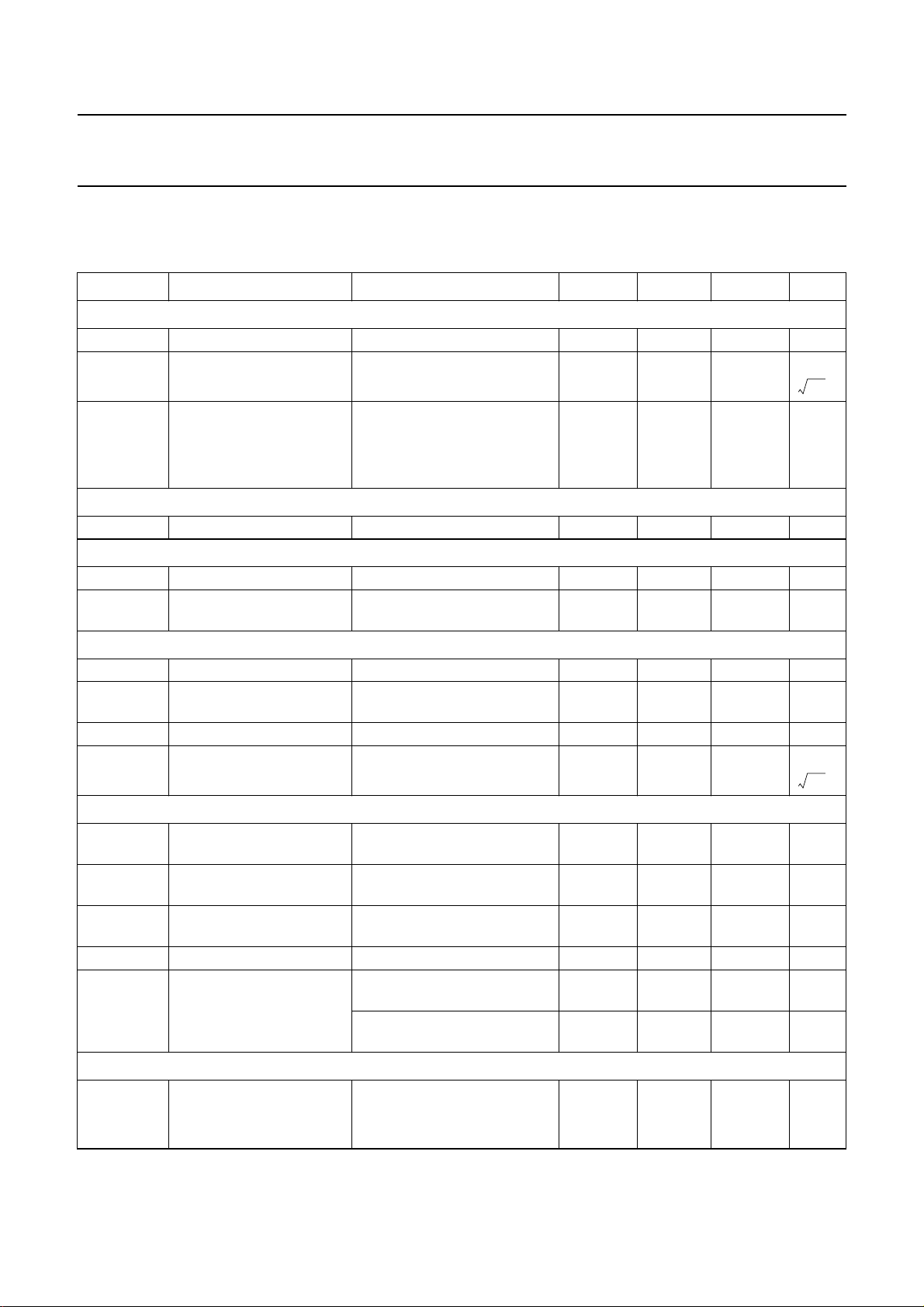
11 AC CHARACTERISTICS
V
DDA1=VDDA3=VDDA4=VDDA5=VDDA6
otherwise specified.
SYMBOL PARAMETER CONDITIONS MIN. TYP. MAX. UNIT
Voltage controlled oscillator
f
osc
oscillator frequency 151.2 − 248.2 MHz
C/N carrier-to-noise ratio f
RR ripple rejection f
FEEDBACK INPUT: PIN OSCFDB
V
i(bias)
input bias voltage 2.2 2.8 3.4 V
TANK CIRCUIT OUTPUT: PIN OSCTNK
V
O
V
o(rms)
DC output voltage 5 6.1 7.2 V
AC output voltage
(RMS value)
Crystal oscillator
f
R
xtal
xtal
crystal frequency 20.4996 20.5 20.5004 MHz
crystal motional
resistance
C
xtal
crystal shunt capacitance −−18 pF
C/N carrier-to-noise ratio f
= 8.5 V; V
= 200 MHz; ∆f = 10 kHz − 101 −
osc
ripple
V
DDA3(ripple)
f
osc
f
osc
f
= 200 MHz − 1.5 − V
osc
DDA2
=5V; V
DDD
=5V; T
=25°C; see Figs 9 and 10; unless
amb
= 100 Hz;
= 100 mV (RMS)
= 250 MHz − 97 − dB
= 200 MHz − 99 − dB
start of operating −−500 Ω
= 20.5 MHz (10.25 MHz);
xtal
− 112 −
∆f=10kHz
dBc
----------- Hz
dBc
----------- Hz
C
IRCUIT INPUTS: PINS XTAL1, XTAL2 AND XTALGND
V
xtal(rms)
crystal voltage
note 1 − 350 − mV
(RMS value)
V
XTAL1
V
XTAL2
R
i
C
i
I
XTALGND
,
DC bias voltage 1.7 2.1 2.5 V
real part of input
impedance
V
XTAL1
note 1
− V
XTAL2
input capacitance note 1 8 10 12 pF
crystal oscillator circuit
current
start-up at
V
XTAL1=VXTAL2
operating at
V
XTAL1
− V
XTAL2
Oscillator divider N1
N1 oscillator divider ratio FM mode:
standard, Europe and local − 2 −
weather band (WX) − 1 −
2001 Mar 08 12
= 1 mV;
= 2.1 V
= ±400 mV
−500 −− Ω
− 9 − mA
− 1.5 − mA
Page 13

Philips Semiconductors Product specification
New In Car Entertainment (NICE) car radio TEA6840H
SYMBOL PARAMETER CONDITIONS MIN. TYP. MAX. UNIT
Oscillator divider N2
N2 oscillator divider ratio AM mode
SW − 10 −
LW and MW − 5 −
Synthesizer
PROGRAMMABLE DIVIDER
N
prog
∆N
step
REFERENCE FREQUENCY DIVIDER
N
ref
CHARGE PUMP: PIN CPOUT
I
sink(cp1)l
I
source(cp1)l
I
sink(cp1)h
I
source(cp1)h
I
sink(cp2)
I
source(cp2)
I
, I
Z(cp1)
CHARGE PUMP: PIN V
I
sink(cp3)
I
source(cp3)
I
Z(cp3)
programmable divider
ratio
programmabledivider step
size
crystal oscillator divider
ratio
low charge pump 1 peak
sink current
low charge pump 1 peak
source current
high charge pump 1 peak
sink current
high charge pump 1 peak
source current
charge pump 2 peak sink
current
charge pump 2 peak
source current
charge pump 1 or 2
Z(cp2)
current in 3-state
tune
charge pump 3 peak sink
current
charge pump 3 peak
source current
charge pump 3 current in
3-state
512 − 32767
− 1 −
f
= 20.5 MHz
xtal
f
= 100 kHz − 205 −
ref
f
= 500 kHz − 410 −
ref
f
= 25 kHz − 820 −
ref
f
= 20 kHz − 1025 −
ref
f
= 10 kHz − 2050 −
ref
FM weather band mode;
0.4V<V
CPOUT
< 7.6 V
FM weather band mode;
0.4V<V
CPOUT
< 7.6 V
AM stereo mode; N2 = 10
200 300 400 µA
−400 −300 −200 µA
0.7 1 1.3 mA
(LWand MW);
0.4V<V
AM stereo mode; N2 = 10
CPOUT
< 7.6 V
−1.3 −1 −0.7 mA
(LWand MW);
0.4V<V
FM standard mode;
0.3V<V
FM standard mode;
0.3V<V
0<V
CPOUT
FM standard mode;
0.4V<V
FM standard mode;
0.4V<V
0<V
tune
< 7.6 V
CPOUT
100 130 160 µA
< 7.1 V
CPOUT
−160 −130 −100 µA
< 7.1 V
CPOUT
< 8.5 V −5 − +5 nA
2.1 3 3.9 mA
< 7.6 V
tune
−3.9 −3 −2.1 mA
< 7.6 V
tune
< 8.5 V −5 − +5 nA
2001 Mar 08 13
Page 14
Philips Semiconductors Product specification
New In Car Entertainment (NICE) car radio TEA6840H
SYMBOL PARAMETER CONDITIONS MIN. TYP. MAX. UNIT
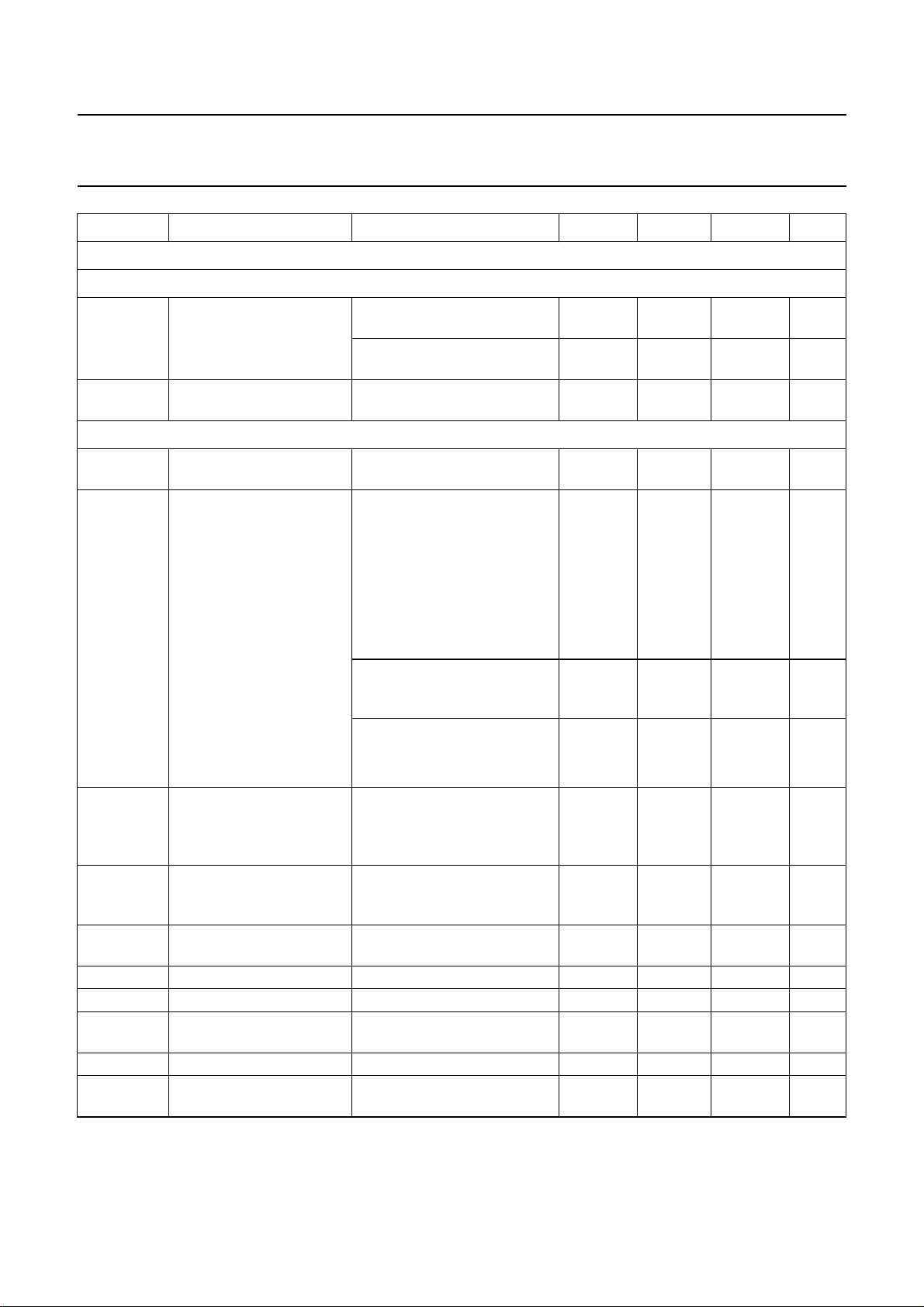
Antenna Digital Auto Alignment (DAA)
DAA INPUT: PIN DAAIN
I
bias(cp)
V
i(cp)
DAA OUTPUT: PIN DAAOUT; note 2
V
o(AM)
V
o(FM)
V
o(n)
∆V
o(T)
∆V
o(step)
I
o(sink)
I
o(source)
t
st
RR ripple rejection f
C
L
charge pump buffer input
bias current
charge pump buffer input
FM mode;
0.4V<V
AM mode;
0V<V
DAAIN
DAAIN
−10 − +10 nA
< 8.0 V
−10 − +10 nA
< 8.5 V
0 − 8.5 V
voltage
DAA output voltage in
−−0.3 V
AM mode
DAA output voltage in
FM mode
V
DAAIN
V
DAATD
= 4.0 V;
= 0.7 V
minimum value −−0.5 V
bits DAA[6:0] set to logic 0 1.5 1.65 1.8 V
value: data
3.8 4 4.2 V
byte 3 = 10101011
maximum value;
8 − 8.5 V
bits DAA[6:0] set to logic 1
V
V
= 3.0 V;
DAAIN
= 0.7 V; bits DAA[6:0]
DAATD
6.2 6.5 6.8 V
set to logic 1
V
DAAIN
=2V
data byte 3 = 11010101 3 3.3 3.6 V
data byte 3 = 10101010 1.8 2 2.2 V
DAA output noise voltage FM mode; V
DAAIN
=4V;
− 30 100 µV
data byte 3: bit 6 = 1,
bits 5 to 0 = 0;
B = 300 Hz to 15 kHz
DAA output voltage
variation with temperature
DAA step accuracy FM mode; V
T
= −40 to +85 °C;
amb
data byte 3 = 10101011;
V
DAATD
= 0.7 V
DAAOUT
< 8.0 V;
−8 − +8 mV
0.5V
LSB
V
LSB
1.5V
LSB
mV
n = 0 to 127
DAA output sink current 0.2V<V
DAAOUT
< 8.25 V 50 −− µA
DAA output source current −−−50 µA
DAA output settling time 0.2V<V
DAAOUT
< 8.25 V;
−−30 µs
CL= 270 pF
DAA output load
ripple
V
DAAOUT
= 100 Hz; V
< 8.0 V; FM mode −−270 pF
=1mV − 50 − dB
DDA4
capacitance
2001 Mar 08 14
Page 15
Philips Semiconductors Product specification
New In Car Entertainment (NICE) car radio TEA6840H
SYMBOL PARAMETER CONDITIONS MIN. TYP. MAX. UNIT
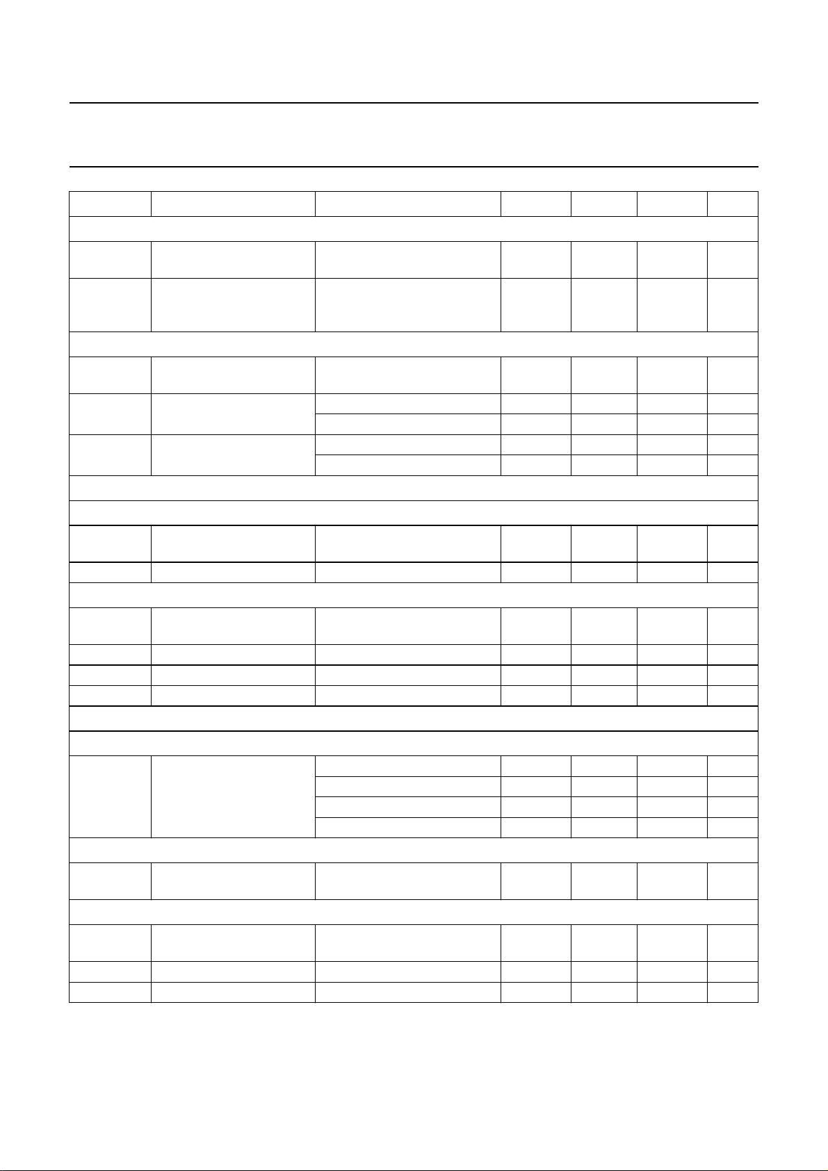
DAA TEMPERATURE COMPENSATION: PIN DAA TD
I
source
TC
source
IF counter (FM IF or AM IF2 counter)
N
IF
T
count(IF)
R
precount
Reference frequency for car sound processor IC; note 3
compensation diode
0.2V<V
< 1.5 V −50 −40 −30 µA
DAATD
source current
temperature coefficient of
compensation diode
0.2V<V
T
= −40 to +85 °C
amb
DAATD
< 1.5 V;
−3 × 10
−10
− +3 × 10
−10K−1
source current
IF counter length for
− 8 − bit
AM and FM
IF counter period data byte 4: bit 7 = 1 − 2 − ms
data byte 4: bit 7 = 0 − 20 − ms
FM IF counter prescaler
ratio
data byte 4: bit 3 = 1 − 10 −
data byte 4: bit 3 = 0 − 100 −
REFERENCE FREQUENCY DIVIDER
N
ref
crystal oscillator divider
ratio
f
ref
VOLTAGE GENERATOR; PIN f
V
o(p-p)
reference frequency f
ref
AC output voltage
= 20.5 MHz − 75.368 − kHz
xtal
(peak-to-peak value)
V
R
R
O
o
L(min)
DC output voltage 3.2 3.4 3.9 V
output resistance −−50 kΩ
minimum load resistance 1 −− MΩ
AM signal channel
AM RF AGC STAGE INPUTS: PINS AMMIX1IN1 AND AMMIX1IN2
V
i(p)
RF input voltage for AGC
start level (peak value)
data byte 5: bit 5 = 0, bit 6 = 0 − 375 − mV
data byte 5: bit 5 = 1, bit 6 = 0 − 500 − mV
data byte 5: bit 5 = 0, bit 6 = 1 − 625 − mV
data byte 5: bit 5 = 1, bit 6 = 1 − 750 − mV
AM IF AGC STAGE INPUTS: PINS AMIF2IN AND AMIF2DEC
V
i(p)
IF2 input voltage (peak
AGC start level 0.5 0.85 1 V
value)
AM RF AGC CURRENT GENERATOR OUTPUT: PIN IAMAGC
I
sink(max)
R
o
C
o
maximum AGC sink
current
output resistance I
V
AMMIX1IN1
(peak value)
IAMAGC
=1µA1−− MΩ
> 500 mV
output capacitance − 57 pF
− 272 −
60 100 170 mV
− 15 − mA
2001 Mar 08 15
Page 16
Philips Semiconductors Product specification
New In Car Entertainment (NICE) car radio TEA6840H
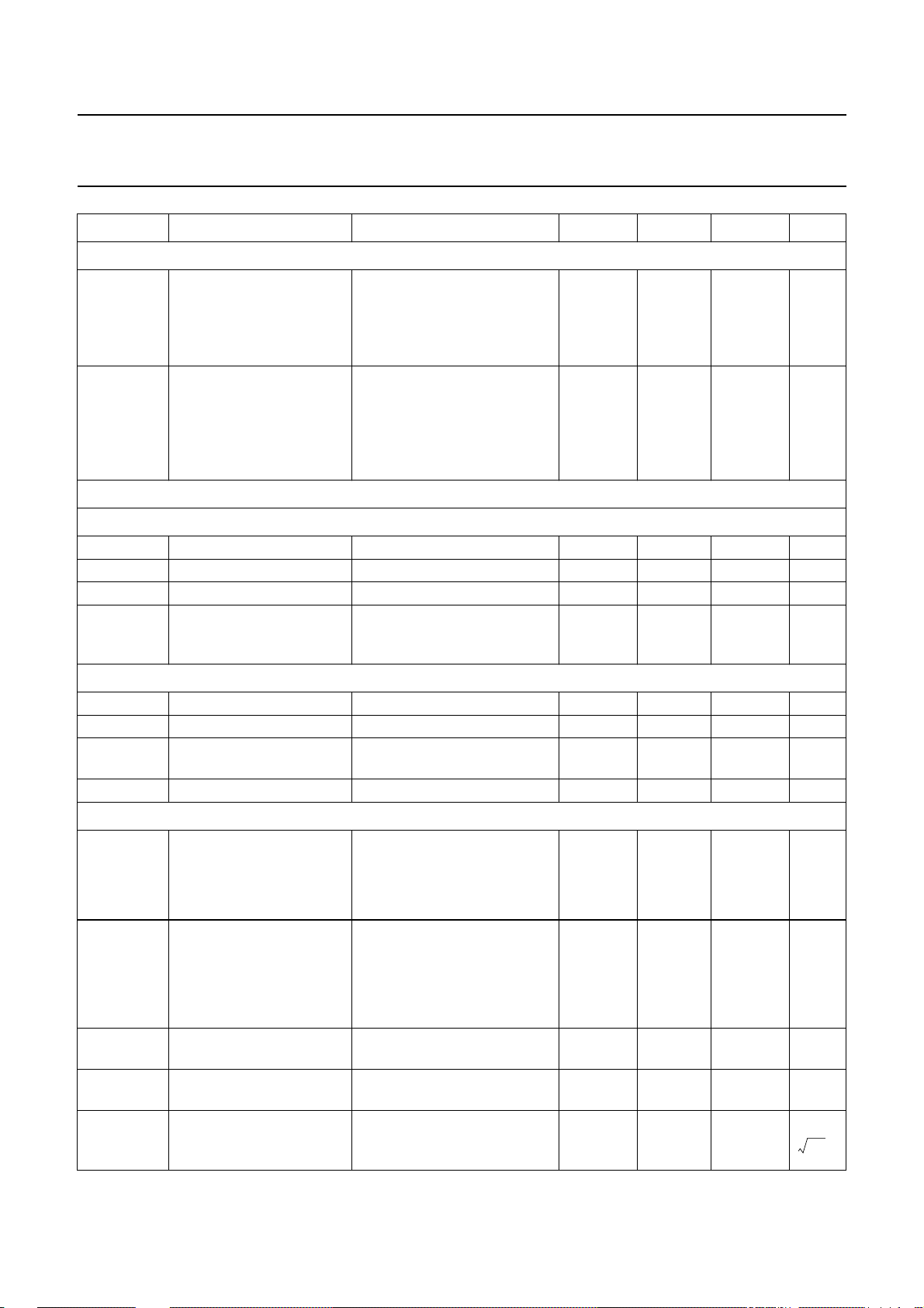
SYMBOL PARAMETER CONDITIONS MIN. TYP. MAX. UNIT
AM RF AGC PEAK DETECTOR: PIN T2AMAGC
I
att
I
dec
AM MIXER 1 (IF1 = 10.7 MHZ)
Mixer inputs: pins AMMIX1IN1 and AMMIX1IN2
R
i
C
i
V
I
V
i(max)
Mixer outputs: pins MIX1OUT1 and MIX1OUT2
R
o
C
o
V
o(max)(p-p)
I
bias
Mixer
g
m(conv)
g
m(conv)(T)
IP3 3rd-order intermodulation RL= 2.8 kΩ(AC loadbetween
IP2 2nd-order intermodulation RL= 2.8 kΩ(AC loadbetween
V
i(n)(eq)
attack current AGC peak
detector
data byte 5: bit 5 = 1,
bit6=1;
−−3.15 − mA
AM mixer 1 input Vi=1V;
decay current AGC peak
detector
V
T2AMAGC−GND
V
AMIF2IN−AMIF2DEC
data byte 5: bit 5 = 1,
bit6=1;
=3V;
=0V
− 2.6 −µA
AM mixer 1 input Vi=0V;
V
T2AMAGC−AMMIX1IN2
V
T2AMAGC−GND
V
AMIF2IN−AMIF2DEC
= 0.25 V;
=3V;
=0V
input resistance note 4 50 70 100 kΩ
input capacitance note 4 − 57 pF
DC input voltage 2.3 2.7 3.1 V
maximum voltage on
pin AMMIX1IN1
1 dB compression point of
AM mixer 1 output
500 −− mV
(peak-to-peak)
output resistance note 5 100 −− kΩ
output capacitance note 5 − 57 pF
maximum output voltage
12 15 − V
(peak-to-peak value)
mixer bias current AM mode 4.8 6 7.2 mA
conversion
transconductance
I
MIXOUT1
--------------------------------------------------V
FMMIXIN1 FMMIXIN2–
conversion
2.0 2.55 3.2
−−9 × 10⁻⁴− K
mA
--------V
−1
transconductance
variation with temperature
g
∆
m(conv)
--------------------------------g
m(conv)
T∆×
135 138 − dBµV
output pins)
− 170 − dBµV
output pins)
equivalent input noise
voltage
band limited noise;
R
= 750 Ω; RL= 2.8 kΩ
gen
(AC load between output pins)
− 5.8 −
nV
----------- -
Hz
2001 Mar 08 16
Page 17
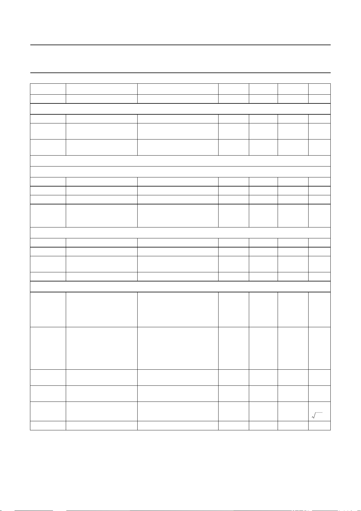
Philips Semiconductors Product specification
New In Car Entertainment (NICE) car radio TEA6840H
SYMBOL PARAMETER CONDITIONS MIN. TYP. MAX. UNIT
F noise figure of AM mixer 1 − 4.5 7.1 dB
WEATHER BAND FLAG: PIN T1AMAGC
I
L(max)
V
o(max)
V
o(min)
AM MIXER 2 (IF2 = 450 kHz)
Mixer inputs: pins IFAMP1IN and IFAMP1DEC
R
i
C
i
V
I
V
i(max)(p)
Mixer outputs: pins AMMIX2OUT1 and AMMIX2OUT2
R
0
C
o
V
o(max)(p-p)
I
bias
Mixer
g
m(conv)
g
m(conv)(T)
IP3 3rd-order intermodulation RL=4kΩ (AC load between
IP2 2nd-order intermodulation RL=4kΩ (AC load between
V
i(n)(eq)
F noise figure of AM mixer 2 − 16 19.5 dB
maximum load current −5 − +5 µA
maximum output voltage
for FM mode
minimum output voltage
for WX mode
measured with respect to
pin RFGND
measured with respect to
pin RFGND
0 − 0.5 V
5.1 6 6.9 V
input resistance note 6 270 330 390 Ω
input capacitance note 6 − 57 pF
DC input voltage 2.4 2.7 3 V
maximum input voltage
(peak value)
1 dB compression point of
AM mixer 2 output
1.1 −− V
(peak-to-peak)
output resistance note 7 100 −− kΩ
output capacitance note 7 − 57 pF
maximum output voltage
V
= 8.5 V 12 15 − V
DDA
(peak-to-peak value)
mixer bias current AM mode 3.6 4.5 5.4 mA
conversion
transconductance
I
AMMIX2OUT1
------------------------------ V
IFAMP1IN
conversion
1.3 1.6 1.9
−−9 × 10⁻⁴− K
mA
--------V
−1
transconductance
variation with temperature
∆
g
m(conv)
--------------------------------g
m(conv)
T∆×
134 137 − dBµV
output pins)
− 170 − dBµV
output pins)
equivalent input noise
voltage
R
= 330 Ω; RL=4kΩ
gen
(AC load between output pins)
− 15 22
nV
----------- -
Hz
2001 Mar 08 17
Page 18
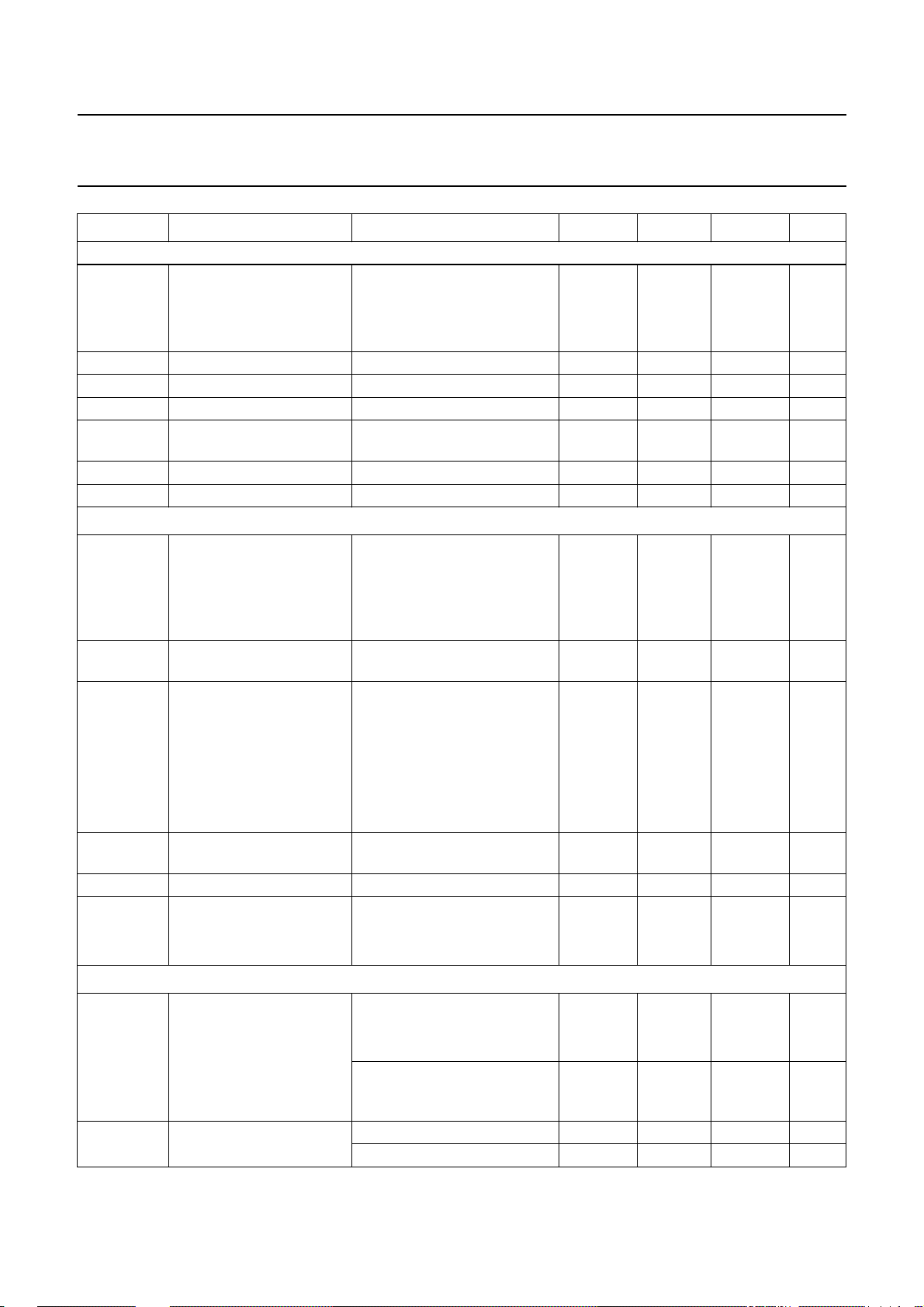
Philips Semiconductors Product specification
New In Car Entertainment (NICE) car radio TEA6840H
SYMBOL PARAMETER CONDITIONS MIN. TYP. MAX. UNIT
AM IF2 AGC STAGE:PINS AMIF2IN AND AMIF2DEC; note 8
V
i
V
AGC(start)
V
AGC(stop)
V
AGC(ctrl)
∆AGC AGC range between start and stop of
R
i
C
i
AM DETECTOR
V
sens(rms)
(S+N)/N maximum signal plus
THD total harmonic distortion BAF= 2.5 kHz; C
RR ripple rejection V
t
sw
t
settle
Output: pin AMAFIF2
V
o(rms)
R
o
input voltage for α = −10 dB audio
attenuation
AM soft mute on − 75 120 µV
AM soft mute off − 610µV
AGC start voltage input carrier voltage − 14 30 µV
AGC stop voltage maximum input peak voltage 1 −− V
AGC control voltage Vi= 1 mV 4.1 4.3 4.7 V
− 89 − dB
AGC; m = 0.8
input resistance 1.8 2 2.2 kΩ
input capacitance −−5pF
sensitivity voltage
(RMS value)
m = 0.3; f
mod
= 400 Hz;
BAF= 2.5 kHz; R
gen
=2kΩ;
note 8
(S+N)/N = 26 dB − 45 65 µV
(S+N)/N = 46 dB − 600 900 µV
noise-to-noise ratio
m = 0.3; f
BAF= 2.5 kHz; R
mod
= 400 Hz;
=2kΩ
gen
=22µF;
AGC
54 60 − dB
AM IF2 AGC input
Vi= 100 µV to 500 mV (RMS)
FM to AM switching time C
AM AGC settling time C
m = 0.8; f
m = 0.9; f
m = 0.8; f
m = 0.9; f
DDA2(ripple)
f
= 100 Hz
ripple
=22µF − 1000 1500 ms
AGC
=22µF
AGC
= 400 Hz − 0.5 1 %
mod
= 400 Hz − 12 %
mod
= 100 Hz − 1.25 2.5 %
mod
= 100 Hz − 1.75 3.5 %
mod
= 100 mV (RMS);
30 40 − dB
normal operation −−1800 ms
test mode −−180 ms
AM IF2 output voltage
(RMS value)
AM stereo; m = 0
minimum at Vi=14µV 1.5 3 4.5 mV
maximum at Vi= 5.0 mV 130 180 230 mV
AM mono; m = 0.3;
f
= 400 Hz;
mod
240 290 340 mV
Vi= 100 µV to 500 mV (RMS)
output resistance AM stereo −−500 Ω
AM mono −−500 Ω
2001 Mar 08 18
Page 19
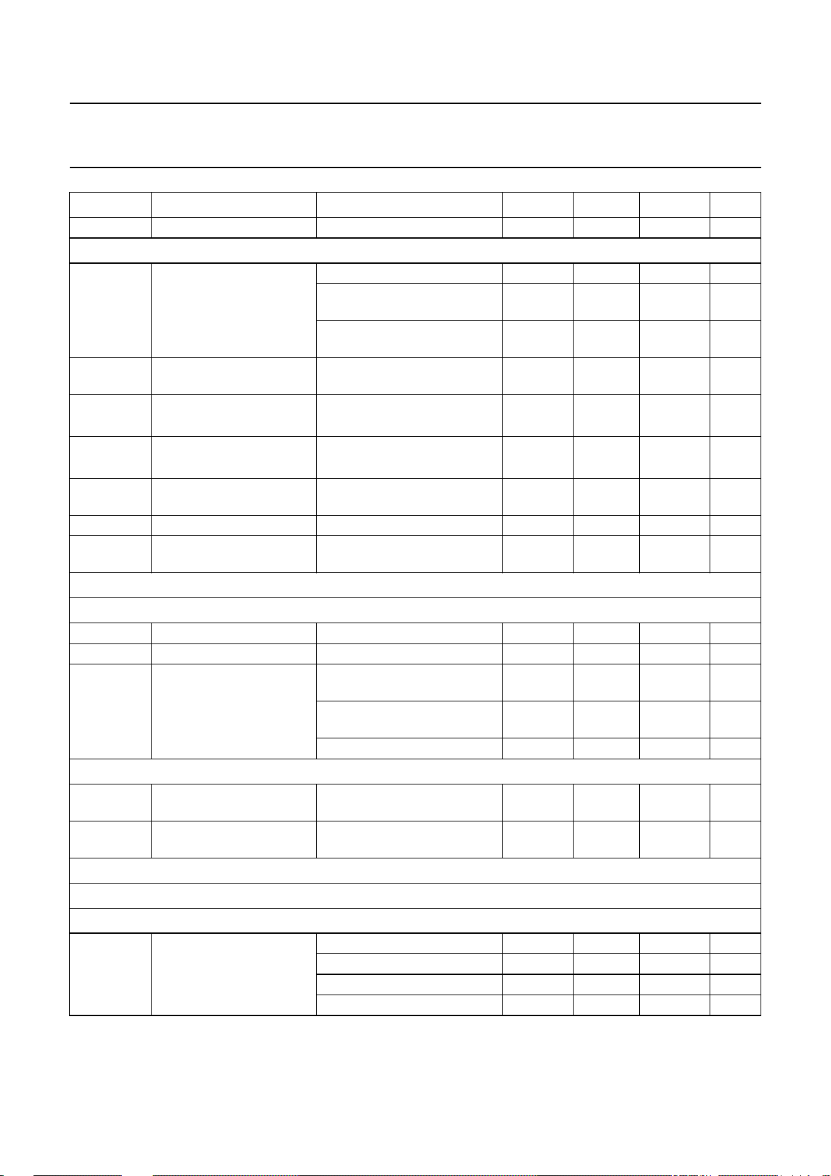
Philips Semiconductors Product specification
New In Car Entertainment (NICE) car radio TEA6840H
SYMBOL PARAMETER CONDITIONS MIN. TYP. MAX. UNIT
C
o
AM IF2 LEVEL DETECTOR OUTPUT: PIN V
V
level
∆V
level
V
level(slope)
∆V
step
B
level
R
o
RR ripple rejection V
AM NOISE BLANKER; see Fig.4
output capacitance AM mono − 57 pF
; see Fig.3
level
DC output voltage Vi=10µVto1V 0 − 7V
Vi<1µV; standard setting of
0.1 0.5 0.9 V
level DAA and level slope
Vi= 1.4 mV; standard setting
1.6 2.2 2.8 V
of level DAA
step size for adjustment of
standard setting of level slope 30 40 50 mV
level starting point
slope of level voltage standard setting of level slope 650 800 950
step size for adjustment of
Vi=1.4 mV 45 60 75
level slope
bandwidth of level output
200 300 − mV
mV
--------------20 dB
mV
--------------20 dB
voltage
output resistance −−500 Ω
DDA1(ripple)
f
= 100 Hz
ripple
= 100 mV (RMS);
− 40 − dB
Threshold: pin AMNBHOLD
V
O
t
sup
f
trigger
DC output voltage 4.3 4.6 5.1 V
suppression time 6 7.5 10 µs
trigger sensitivity
frequency
Noise detector output: pin TRDSMUTE
I
sink(AGC)
AM noise blanker AGC
sink current
V
AGC
AM noise blanker AGC
voltage
FM signal channel
FM RF AGC
Inputs: pins FMMIXIN1 and FMMIXIN2;
V
i(RF)(rms)
RF input voltage for start
of wide-band AGC
(RMS value)
VP= 200 mV (peak);
V
< 1.8 V
level
VP= 200 mV (peak);
V
> 2.2 V
level
− 1000 − Hz
−−100 Hz
VP= 20 mV (peak) −−100 Hz
V
TRDSMUTE
=3V 35 50 65 µA
AM mixer 1 input Vi= 0 V 1.9 2.2 2.5 V
note 9
data byte 5: bit 5 = 0, bit 6 = 0 − 4 − mV
data byte 5: bit 5 = 1, bit 6 = 0 − 8 − mV
data byte 5: bit 5 = 0, bit 6 = 1 − 12 − mV
data byte 5: bit 5 = 1, bit 6 = 1 − 16 − mV
2001 Mar 08 19
Page 20
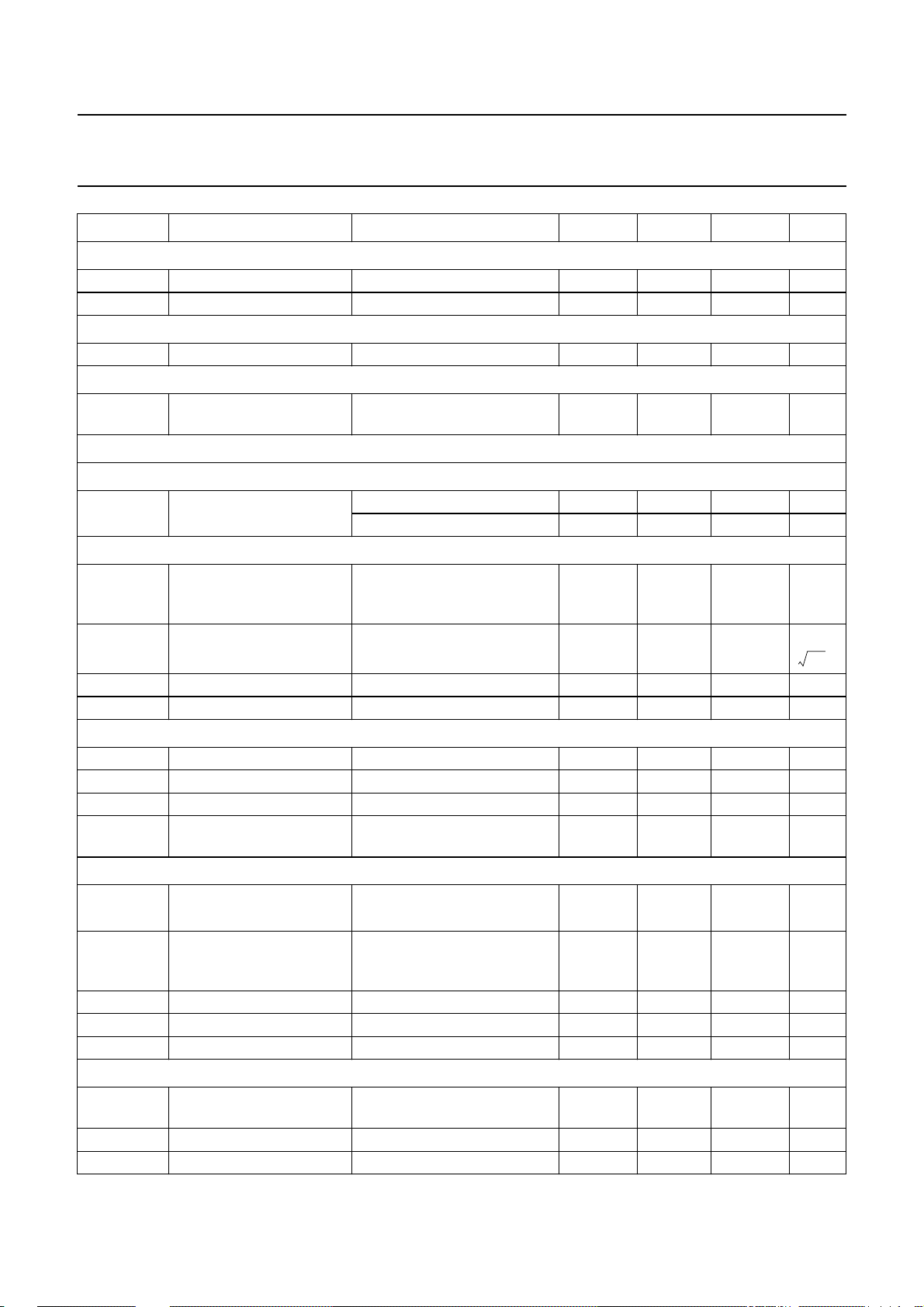
Philips Semiconductors Product specification
New In Car Entertainment (NICE) car radio TEA6840H
SYMBOL PARAMETER CONDITIONS MIN. TYP. MAX. UNIT
AGC peak detector output: pin T1FMAGC
I
ch
I
dis
PIN diode drive output: pin IFMAGC
I
drive
Level voltage output: pin V
V
th
FM RF MIXER
charge current −350 −600 −850 µA
discharge current 15 25 35 µA
drive current Vo= 0.5 to 4.0 V 8 11.5 15 mA
level
threshold voltage for
narrow-band AGC
data byte 5 bit 7 = 1; standard
setting of level DAA
500 950 1400 mV
Reference voltage: pin V
V
ref
reference voltage FM mode 6.5 7.1 7.9 V
ref(FMMIX)
AM mode 2.7 3.1 3.4 V
Inputs: pins FMMIXIN1 and FMMIXIN2;
V
i(RF)(max)
maximum RF input
voltage
note 9
1 dB compression point of
FM mixer output voltage
70 100 − mV
(peak-to-peak value)
V
i(n)(eq)
R
i
C
i
Outputs: pins MIX1OUT1 and MIX1OUT2;
R
o
C
o
I
bias
V
o(max)(p-p)
equivalent input noise
voltage
R
= 600 Ω; RL= 2.8 kΩ;
gen
noise of R
not included
gen
− 2.6 3.1
nV
----------- Hz
input resistance − 1.4 − kΩ
input capacitance − 57 pF
note 5
output resistance 100 −− kΩ
output capacitance − 57 pF
mixer bias current FM mode 4.8 6 7.2 mA
maximum output voltage
3 −− V
(peak-to-peak value)
FM mixer
g
m(conv)
g
m(conv)(T)
conversion
transconductance
conversion
8.5 12.5 18
−−1 × 10⁻³− K
mA
---------
V
−1
transconductance
variation with temperature
F noise figure − 3 4.6 dB
IP3 3rd-order intermodulation 116 119 − dBµV
IRR image rejection ratio 25 30 − dB
IF AMPLIFIER 1
G gain RL= 330 Ω; Vi=1mV;
8.5 10.5 12.5 dB
note 10
F noise figure − 9.5 13 dB
IP3 3rd-order intermodulation 120 123 − dBµV
2001 Mar 08 20
Page 21
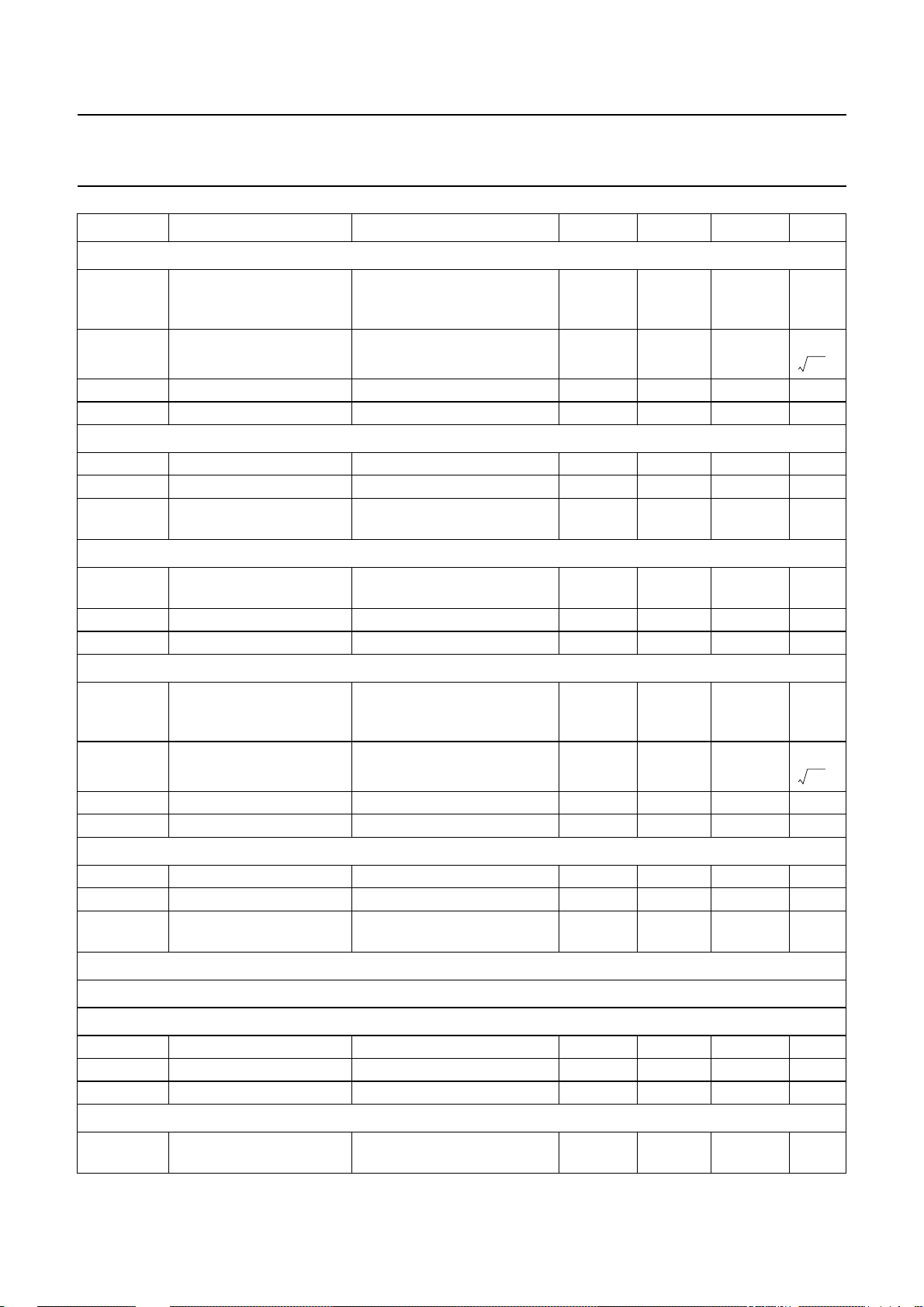
Philips Semiconductors Product specification
New In Car Entertainment (NICE) car radio TEA6840H
SYMBOL PARAMETER CONDITIONS MIN. TYP. MAX. UNIT
Inputs: pins IFAMP1IN and IFAMP1DEC;
V
i(max)(p)
maximum input voltage
(peak value)
note 10
1 dB compression point of
IF amplifier 1 output voltage
300 −− mV
(peak value)
V
i(n)(eq)
R
i
C
i
equivalent input noise
voltage
R
= 330 Ω; RL= 330 Ω;
gen
noise of R
not included
gen
− 710
nV
----------- Hz
input resistance 270 330 390 Ω
input capacitance − 57 pF
Output: pin IFAMP1OUT
R
o
C
o
V
o(max)(p)
output resistance 270 330 390 Ω
output capacitance − 57 pF
maximum output voltage
1.2 1.5 − V
(peak value)
IF AMPLIFIER 2
G gain RL= 330 Ω; Vi=1mV;
3 4.5 6 dB
note 11
F noise figure − 12 15 dB
IP3 3rd-order intermodulation 129 132 − dBµV
Inputs: pins IFAMP2IN and IFAMP2DEC;
V
i(max)(p)
maximum input voltage
(peak value)
note 11
1 dB compression point of
IF amplifier 2 output voltage
600 −− mV
(peak value)
V
i(n)(eq)
R
i
C
i
equivalent input noise
voltage
R
= 330 Ω; RL= 330 Ω;
gen
noise of R
not included
gen
− 912
nV
----------- Hz
input resistance 270 330 390 Ω
input capacitance − 57 pF
Output: pin IFAMP2OUT
R
o
C
o
V
o(max)(p)
output resistance 270 330 390 Ω
output capacitance − 57 pF
maximum output voltage
1.2 1.5 − V
(peak value)
FM demodulator and level detector; see Figs 5 and 6
FM LIMITER
Inputs: pins FMLIMIN and FMLIMDEC;
G gain R
R
i
C
i
input resistance 270 330 390 Ω
input capacitance − 57 pF
note 12
gen
=50Ω 74 80 − dB
Outputs: pins QDET1 and QDET2
V
o(p-p)
output voltage
(peak-to-peak value)
measured between output
pins
2001 Mar 08 21
500 700 − mV
Page 22
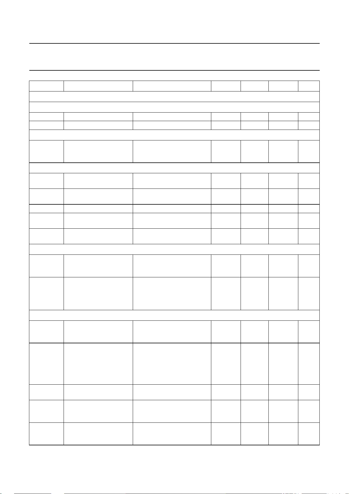
Philips Semiconductors Product specification
New In Car Entertainment (NICE) car radio TEA6840H
SYMBOL PARAMETER CONDITIONS MIN. TYP. MAX. UNIT
FM DEMODULATOR
Limiter decoupling: pin FMLIMDEC
R
L
C
L
RDS MPX inputs: pins FMLIMIN and FMLIMDEC;
V
start(lim)(rms)
RDS MPX output: pin QRDSMPX
V
o(rms)
I
o(max)
R
o
B bandwidth RDS MPX
PSRR power supply ripple
FM RDS inputs: pins FMLIMIN and FMLIMDEC;
V
start(lim)(rms)
V
o(sens)(rms)
FM MPX output: pin FMMPX;
V
o(rms)
α
AM
I
o(max)
(S+N)/N maximum signal plus
THD totalharmonic distortion of
load resistance 20 −− kΩ
load capacitance −−50 pF
note 12
start of limiting of RDS
αAF= −3dB − 10 15 µV
MPX output voltage
(RMS value)
RDS MPX output voltage
(RMS value)
maximum RDS MPX
∆f = 22.5 kHz; f
mod
= 57 kHz;
Vi=20µV to 1 V; note 12
180 230 280 mV
−−100 µA
output current
output resistance −−500 Ω
CL= 0; RL>20kΩ 200 300 − kHz
output
f
= 100 Hz to 20 kHz − 40 − dB
ripple
rejection
note 12
start of limiting of MPX
αAF= −3dB − 10 15 µV
output voltage
(RMS value)
sensitivity for MPX output
voltage (RMS value)
∆f = 22.5 kHz; f
mod
de-emphasis = 75 µs
= 1 kHz;
(S+N)/N = 26 dB − 10 15 µV
(S+N)/N = 46 dB − 50 75 µV
note 12
MPX output voltage
(RMS value)
∆f = 22.5 kHz; f
mod
= 1 kHz;
de-emphasis = 75 µs;
180 230 280 mV
Vi=20µVto1V
AM suppression of MPX
output
∆f = 22.5 kHz; f
mod
= 1 kHz;
m = 0.3; de-emphasis = 75 µs
Vi= 500 µV to 300 mV 50 60 − dB
Vi=20to500µV − 40 − dB
Vi= 300 mV to 1 V − 40 − dB
maximum MPX output
−−100 µA
current
noise-to-noise ratio of
MPX output voltage
MPX output voltage
∆f = 22.5 kHz; f
de-emphasis = 75 µs;
Vi=10mV
∆f = 75 kHz; f
de-emphasis = 75 µs;
mod
mod
= 1 kHz;
= 1 kHz;
67 70 − dB
− 0.35 0.7 %
Vi= 200 µV to 800 mV
2001 Mar 08 22
Page 23
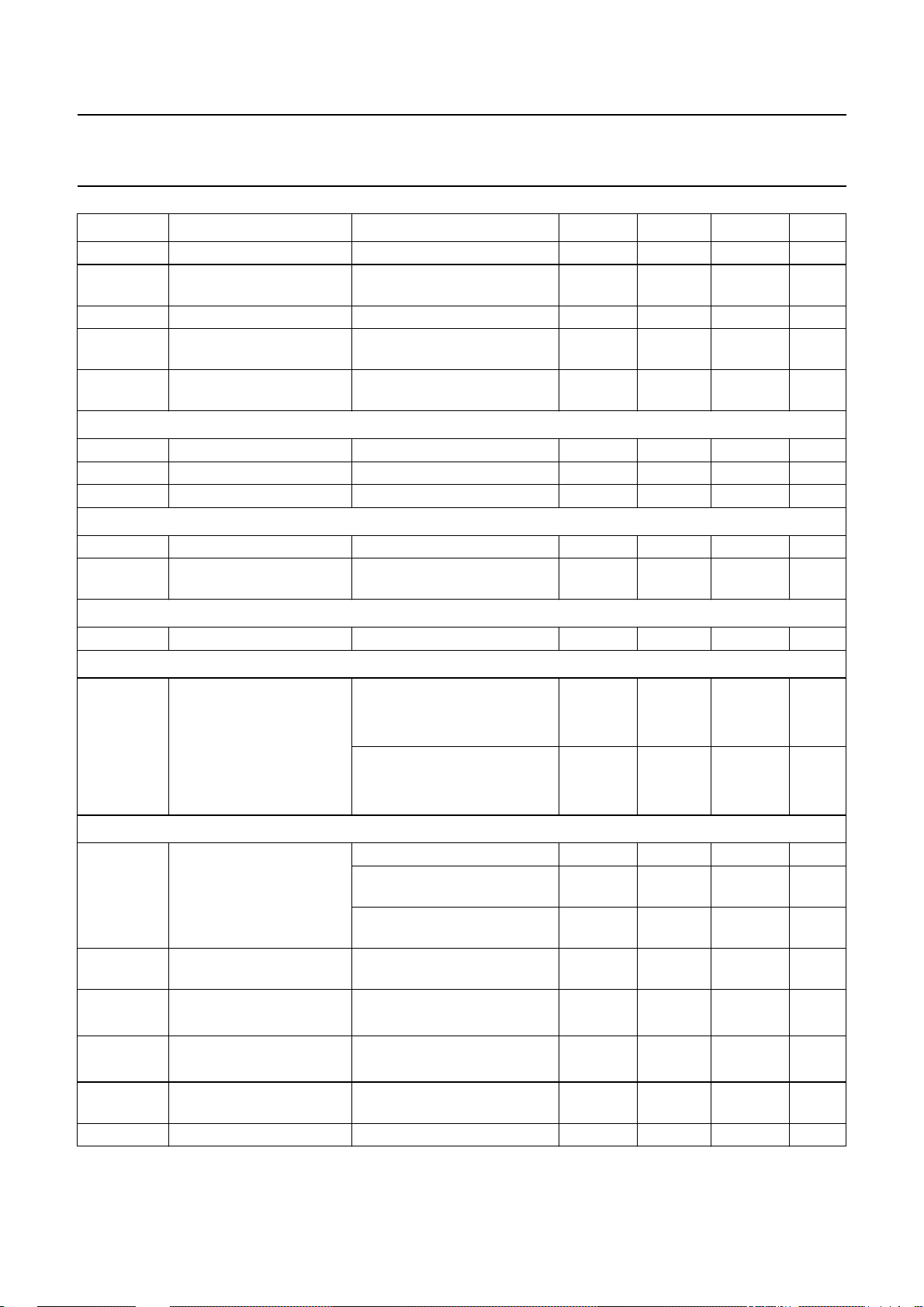
Philips Semiconductors Product specification
New In Car Entertainment (NICE) car radio TEA6840H
SYMBOL PARAMETER CONDITIONS MIN. TYP. MAX. UNIT
B bandwidth MPX output CL= 0; RL>20kΩ 200 −− kHz
PSRR power supply ripple
rejection
R
R
L(min)
o(max)
minimum load resistance 20 −− kΩ
maximum output
resistance
C
L(max)
maximum load
capacitance
MPX MUTE
α
mute
t
att
t
decay
muting depth during RDS update 60 80 − dB
attack time MPX mute C
decay time MPX mute C
RDS update: pin TRDSMUTE
I
dis
I
ch
discharge current Vo= 3 V; audio output muted 24 32 38 µA
charge current Vo= 3 V; audio output not
DEMODULATOR AFC
G
AFC
RDS MPX output: pin RDSMPX;
V
offset(DC)
AFC gain ∆f = 100 kHz 28 32 − dB
note 12
residual DC offset voltage L
FM IF LEVEL DETECTOR OUTPUT: PIN V
V
∆V
level
level
DC output voltage Vi=10µVto1V 0 − 7V
level starting point for
adjustment of step size
V
level(slope)
∆V
step
slope of level voltage standard setting of level slope 650 800 950
level slope adjustment of
step size
B
level
bandwidth of level output
voltage
R
o
output resistance −−500 Ω
f
= 100 Hz to 20 kHz − 40 − dB
ripple
−−500 Ω
−−50 pF
TRDSMUTE
TRDSMUTE
= 10 nF 0.75 1 1.25 ms
= 10 nF 0.75 1 1.25 ms
−24 −32 −38 µA
muted
= typical value
demod
Vi=10to80µV − 0.1 1 V
Vi=80µV to 800 mV − 10 30 mV
L
= ±6%
demod
Vi=10to80µV − 0.240 1 V
Vi=80µV to 800 mV − 25 500 mV
; note 12
level
Vi<1µV; standard setting of
0.1 0.35 0.9 V
level DAA
Vi= 1 mV; standard setting of
1 1.5 2.1 V
level DAA
standard setting of level slope 30 40 50 mV
Vi= 1 mV 45 50 75
Vi=10mV; f
= 22.5 kHz;
mod
200 300 − mV
standard setting of DAA
mV
--------------20 dB
mV
--------------20 dB
2001 Mar 08 23
Page 24
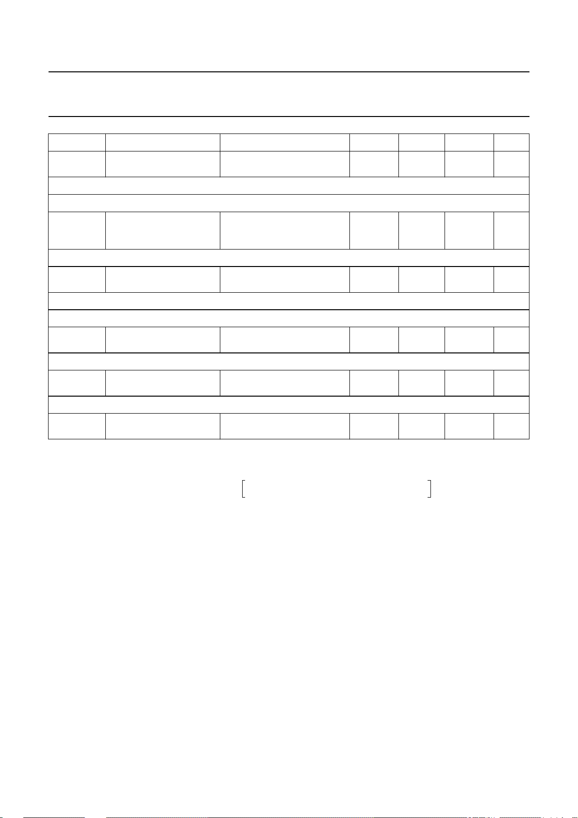
Philips Semiconductors Product specification
New In Car Entertainment (NICE) car radio TEA6840H
SYMBOL PARAMETER CONDITIONS MIN. TYP. MAX. UNIT
RR ripple rejection V
f
ripple
RDS update
Output: pin AFHOLD
I
sink(max)
maximum sink current after first bus transmission
with AF = 1 (start of RDS
update); Vo= 0.5 V
Output: pin AFSAMPLE
I
sink(max)
maximum sink current no RDS update in progress;
Vo= 0.5 V
Test mode; note 3
Temperature compensation diode: pin DAATD
V
i(ext)
external input voltage to
clock state-machine
V
V
Clock input: pin SCL
V
i(ext)
external input voltage to
V
clock DAA
Time constant output: pin T1AMAGC
V
pulse
enabling voltage of load
pin f
PLL signal
DDA1(ripple)
DAATD(L)
DAATD(H)
SCL(L)
ref
= 100 mV (RMS);
− 40 − dB
= 100 Hz
1.0 1.2 1.4 mA
1.0 1.2 1.4 mA
= 2.5 V;
2.5 − 3.5 V
= 3.5 V
=0V; V
=5V 0 − 5V
SCL(H)
in test mode 5.1 6 6.9 V
Notes
1. Measured between pins XTAL1 and XTAL2.
2. DAA conversion gain formula:
V
DAAOUT
2 0.75
× V
n
--------- 128
0.25+×
+()× V
DAAINVDAATD
–=
where n = 0 to 127.
3. Reference frequency pin f
a) R
b) R
=68kΩ connected to ground activates the 2nd I2C-bus address
ext
= 100 kΩ connected to V
ext
ref
:
sets the IC into test mode.
DDA1
4. Input parameters of AM mixer 1 measured between pins AMMIX1IN1 and AMMIX1IN2.
5. Output parameters of FM and AM mixer 1 measured between pins MIX1OUT1 and MIX1OUT2.
6. Input parameters of AM mixer 2 measured between pins IFAMP1IN and IFAMP1DEC.
7. Output parameters of AM mixer 2 measured between pins AMMIX2OUT1 and AMMIX2OUT2.
8. Input parameters of AM IF2 measured between pins AMIF2IN and AMIF2DEC.
9. Input parameters of FM mixer measured between pins FMMIXIN1 and FMMIXIN2.
10. Input parameters of IF amplifier 1 measured between pins IFAMP1IN and IFAMP1DEC.
11. Input parameters of IF amplifier 2 measured between pins IFAMP2IN and IFAMP2DEC.
12. Input parameters of FM limiter measured between pins FMLIMIN and FMLIMDEC.
DAATD
2001 Mar 08 24
Page 25
Philips Semiconductors Product specification
New In Car Entertainment (NICE) car radio TEA6840H
V
6
level
handbook, full pagewidth
(V)
5
4
3
2
1
0
−3
10
−2
10
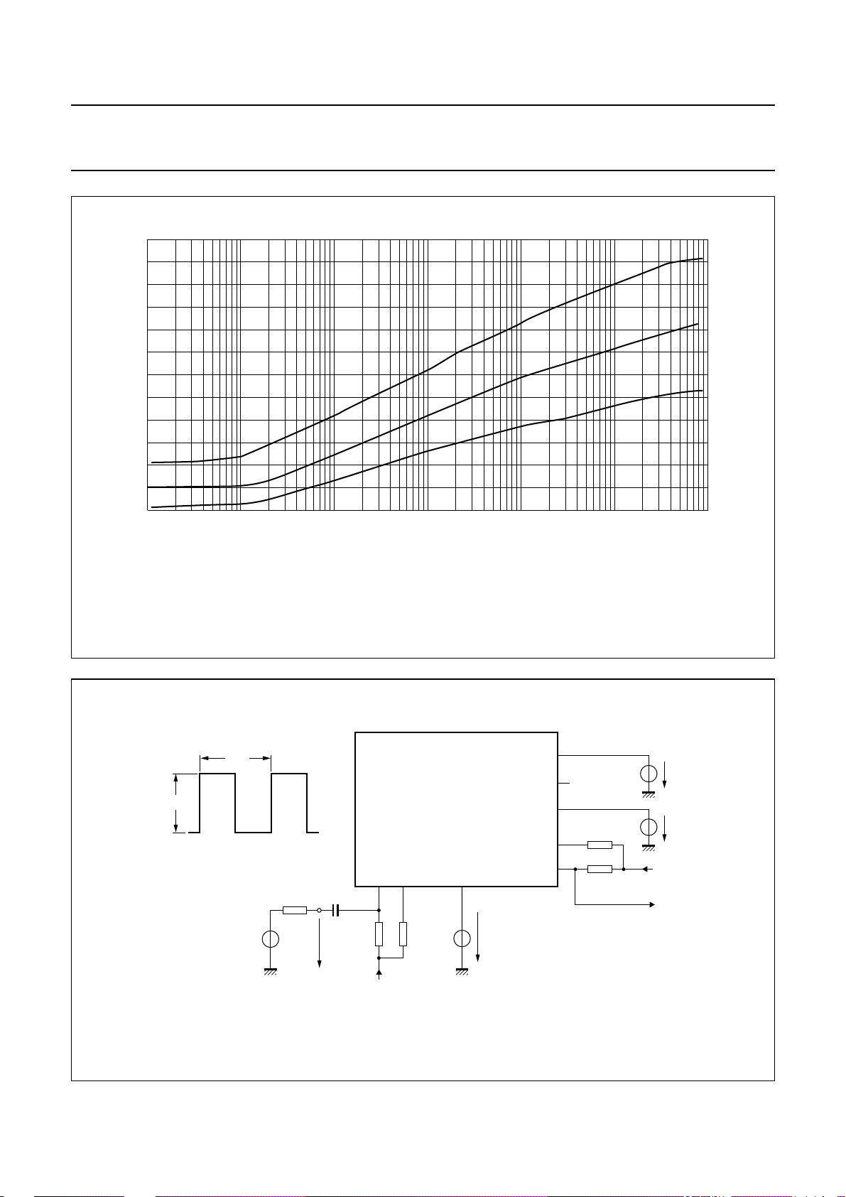
(1) Level DAA setting byte 6 = FFH.
(2) Level DAA setting byte 6 = 84H (standard setting).
(3) Level DAA setting byte 6 = 00H.
Fig.3 AM level output voltage (DAA) as a function of AM level circuit input voltage.
MHB484
(1)
(2)
(3)
−1
10
110
10
Vi=V
2
AMIF2IN
Vi (mV)
− V
AMIF2DEC
3
10
handbook, full pagewidth
T
rep
V
P
test signal
35
36
4.7 nF
50 Ω
100 Ω
V
P
100 Ω
8.5 V
Test signal: T
= 2 ms, tr< 50 ns, tf< 50 ns, and duty factor 50%.
rep
Fig.4 Test circuit for AM noise blanker.
2001 Mar 08 25
TEA6840H
39
4 V
58
V
57
level
55
1 kΩ
3 V
53
52
1 kΩ
8.5 V
oscilloscope,
counter
MHB485
Page 26
Philips Semiconductors Product specification
New In Car Entertainment (NICE) car radio TEA6840H
V
6
level
handbook, full pagewidth
(V)
5
4
3
2
1
0
−3
10
−2
10
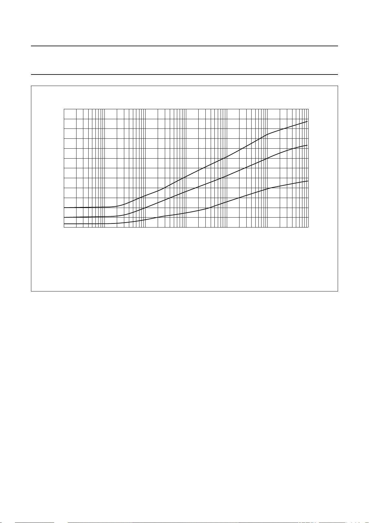
(1) Level DAA setting byte 6 = FFH.
(2) Level DAA setting byte 6 = 84H (standard setting).
(3) Level DAA setting byte 6 = 00H.
Fig.5 FM level output voltage (DAA) as a function of FM limiter and level circuit input voltage.
MHB486
(1)
(2)
(3)
−1
10
110
Vi=V
2
10
FMLIMIN
Vi (mV)
− V
FMLIMDEC
3
10
.
2001 Mar 08 26
Page 27
Philips Semiconductors Product specification
New In Car Entertainment (NICE) car radio TEA6840H
MHB487
V
FMMPX
V
RDSMPX
(dB)
10
,
0
handbook, full pagewidth
−10
(1)
9
V
8
7
level
(V)
THD
(%)
−20
−30
−40
(2)
(3)
−50
−60
(4)
−70
(5)
−80
−3
10
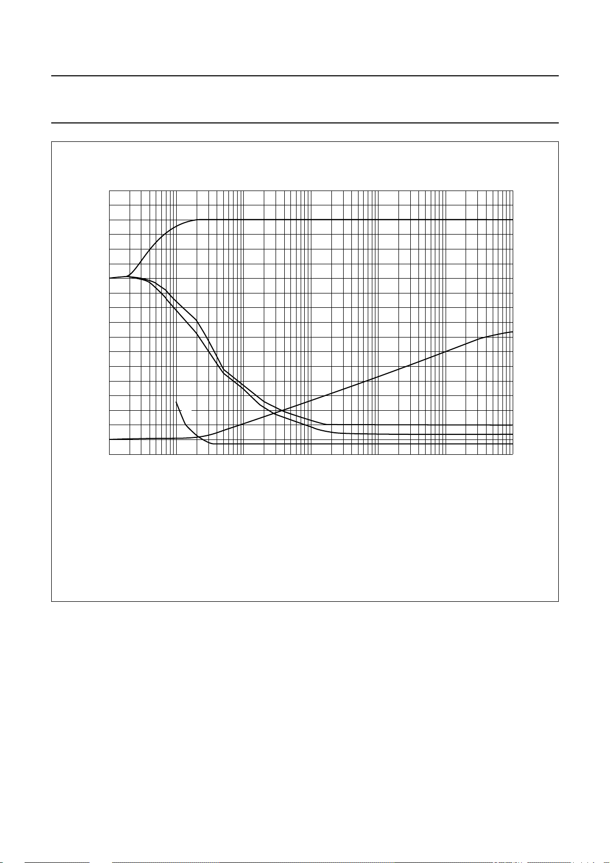
(1) Output voltage for FMMPX and RDSMPX: fIF= 10.7 MHz; ∆f = 22.5 kHz; f
−2
10
−1
10
11010210
mod
(2) Noise: unweighted B = 250 Hz to 15 kHz with de-emphasis 50 µs for FMMPX.
(3) Noise: unweighted B = 250 Hz to 15 kHz with de-emphasis 50 µs for RDSMPX.
(4) THD for FMMPX and RDSMPX.
(5) Level for standard setting of level DAA, byte 6 = 84H.
= 1 kHz.
Vi=V
FMLIMIN
− V
Vi (mV)
FMLIMDEC
6
5
4
3
2
1
0
3
.
Fig.6 (S+N)/N, THD and level output voltage for FM mode as a function of FM demodulator input voltage.
2001 Mar 08 27
Page 28

Philips Semiconductors Product specification
New In Car Entertainment (NICE) car radio TEA6840H
12 I2C-BUS PROTOCOL
2
12.1 I
C-bus specification
The standard I2C-bus specification is expanded by the
following definitions.
IC addresses:
• 1st IC address C2: 1100001
• 2nd IC address C0: 1100000.
2
Structure of the I
C-bus logic: slave transceiver with auto
increment.
Subaddresses are not used.
12.1.1 TEST MODE
Connecting pin f
ref
to V
via a 100 kΩ resistor or
DDA1
feeding 50 µA into that pin switches the IC into the test
mode.
During test mode the digital-to-analog converters of the
levelandantenna DAA functions can be sequenced by the
I2C-bus SCL line.
During test mode either the TEA6880H or TEF6890H
reference frequency, the PLL reference frequency divider
or the programmable divider output can be switched to
pin f
.
ref
12.1.3 I2C-bus pULL-UP RESISTORS
When the IC is used together with the TEA6880H or
TEF6890HandbothSCLandSDAlinesareconnectedvia
the I2C-bus to the CASP, the pull-up resistors of the
tuner IC should be connected to the digital supply voltage
of the TEA6880H or TEF6890H. Otherwise a I2C-bus
pull-downcanoccurswitchingoffthetuner IC supply when
the I2C-bus buffer interface of the TEA6880H or
TEF6890H is enabled for data transfer to the tuner IC.
12.1.4 FREQUENCY SETTING
For new frequency setting, in both AM and FM mode, the
programmable divider is enabled by setting bit MUTE =1.
To select an FM frequency, two I2C-bus transmissions are
necessary:
• First: bit MUTE = 1
• Second: bit MUTE = 0.
12.1.2 DATA TRANSFER FOR THE TEA6840H
Data sequence: address, byte 1, byte 2, byte 3, byte 4,
byte 5, and byte 6.
The data transfer has to be in this order. The LSB = 0
indicates a WRITE operation to the TEA6840H.
Bit 7 of each byte is considered the MSB and has to be
transferred as the first bit of the byte.
The data becomes valid at the output of the internal
latches with the acknowledge of each byte. A STOP
condition after any byte can shorten transmission times.
When writing to the transceiver by using the STOP
condition before completion of the whole transfer:
• The remaining bytes will contain the old information
• If the transfer of a byte is not completed, this byte is lost
and the previous information is available.
In byte 5, 4 bits are reserved for test mode purposes.
Those can only be used when the test mode is activated
by the select pin f
ref.
2001 Mar 08 28
Page 29
Philips Semiconductors Product specification
New In Car Entertainment (NICE) car radio TEA6840H
12.2 I2C-bus protocol
12.2.1 DATA TRANSFER MODE AND IC ADDRESS
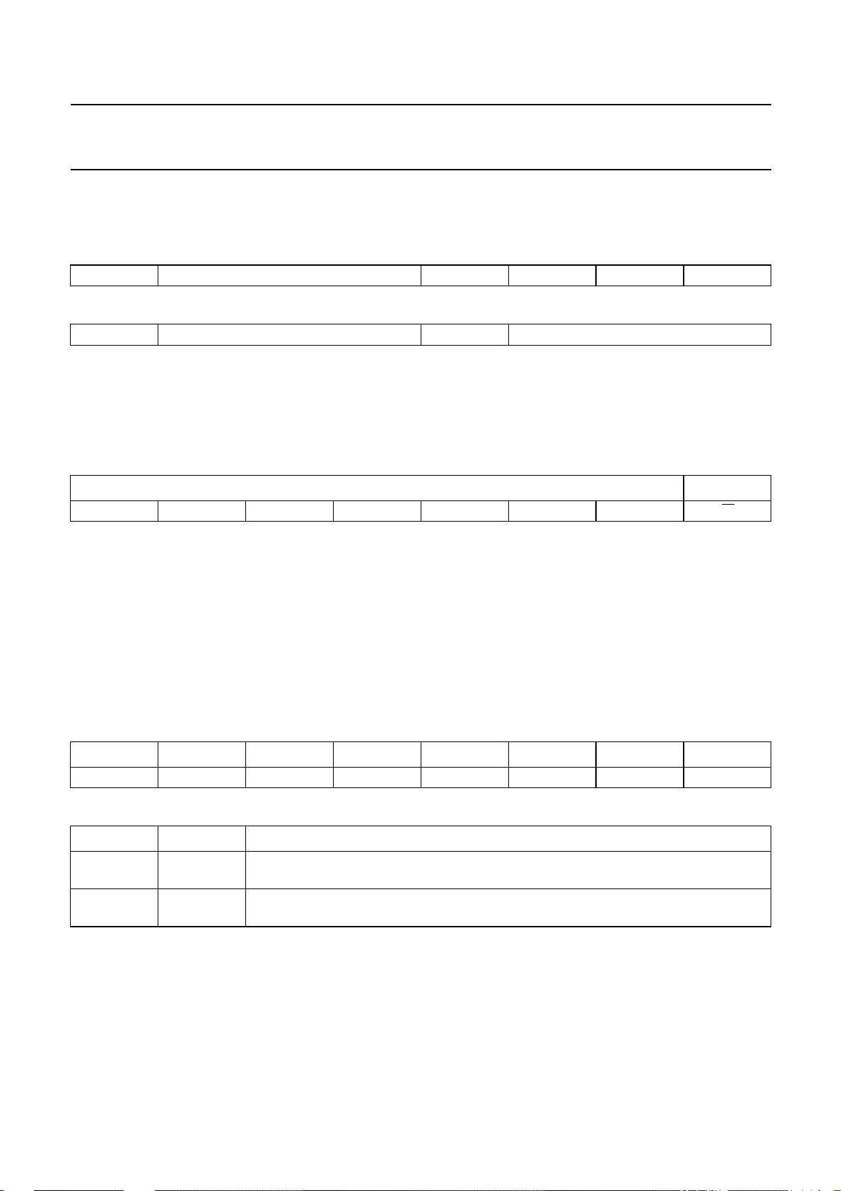
Table 1 Write mode
(1)
S
address (write) A
Table 2 Read mode
(1)
S
address (read) A
Notes
1. S = START condition.
2. A = acknowledge.
3. P = STOP condition.
Table 3 IC address byte
IC ADDRESS MODE
1100000/1
(2)
(2)
data byte(s) A
data byte 1
(2)
(1)
P
R/W
(3)
(2)
Notes
1. Defined by address pin f
ref
:
a) 1 = 1st IC address
b) 0 = 2nd IC address.
2. Read or write mode:
a) 0 = write operation to TEA6840H
b) 1 = read operation from TEA6840H.
12.2.2 WRITE MODE: DATA BYTE 1
Table 4 Format of data byte 1
BIT 7 BIT 6 BIT 5 BIT 4 BIT 3 BIT 2 BIT 1 BIT 0
AF PCA6 PCA5 PCA4 PCA3 PCA2 PCA1 PCA0
Table 5 Description of data byte 1 bits
BIT SYMBOL DESCRIPTION
7AFAlternative frequency. If AF = 0, then normal operation. If AF = 1, then AF (RDS)
update mode.
6 to 0 PCA[6:0] Setting of programmable counter of synthesizer PLL. Upper byte of PLL divider
word.
2001 Mar 08 29
Page 30
Philips Semiconductors Product specification
New In Car Entertainment (NICE) car radio TEA6840H
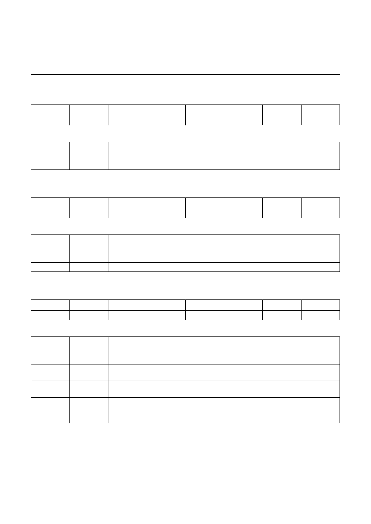
12.2.3 WRITE MODE: DATA BYTE 2
Table 6 Format of data byte 2
BIT 7 BIT 6 BIT 5 BIT 4 BIT 3 BIT 2 BIT 1 BIT 0
PCB7 PCB6 PCB5 PCB4 PCB3 PCB2 PCB1 PCB0
Table 7 Description of data byte 2 bits
BIT SYMBOL DESCRIPTION
7 to 0 PCB[7:0] Setting of programmable counter of synthesizer PLL. Lower byte of PLL divider
word.
12.2.4 WRITE MODE: DATA BYTE 3
Table 8 Format of data byte 3
BIT 7 BIT 6 BIT 5 BIT 4 BIT 3 BIT 2 BIT 1 BIT 0
MUTE DAA6 DAA5 DAA4 DAA3 DAA2 DAA1 DAA0
Table 9 Description of data byte 3 bits
BIT SYMBOL DESCRIPTION
7 MUTE FM audio mute. If MUTE = 0, then FM audio not muted. If MUTE = 1, then FM audio
muted; writing to programmable divider enabled.
6 to 0 DAA[6:0] Setting of antenna digital auto alignment.
12.2.5 WRITE MODE: DATA BYTE 4
Table 10 Format of data byte 4
BIT 7 BIT 6 BIT 5 BIT 4 BIT 3 BIT 2 BIT 1 BIT 0
IFMT RFS2 RFS1 RFS0 IFPR BND1 BND0 AMFM
Table 11 Description of data byte 4 bits
BIT SYMBOL DESCRIPTION
7 IFMT IF measuring time. If IFMT = 0, then IF measuring time is 20 ms. If IFMT = 1, then
IF measuring time is 2 ms.
6 to 4 RFS[2:0] Reference frequency for synthesizer. These 3 bits determine the reference
frequency, see Table 12.
3 IFPR IF counter prescaler ratio. If IFPR = 0, then IF prescaler ratio is 100. If IFPR = 1, then
IF prescaler ratio is 10.
2 and 1 BND[1:0] Band switch. These 2 bits select in FM mode band and local or distant, see Table13;
in AM mode band and AM stereo, see Table 14.
0 AMFM AM or FM switch. If AMFM = 0, then FM mode. If AMFM = 1, then AM mode
2001 Mar 08 30
Page 31
Philips Semiconductors Product specification
New In Car Entertainment (NICE) car radio TEA6840H
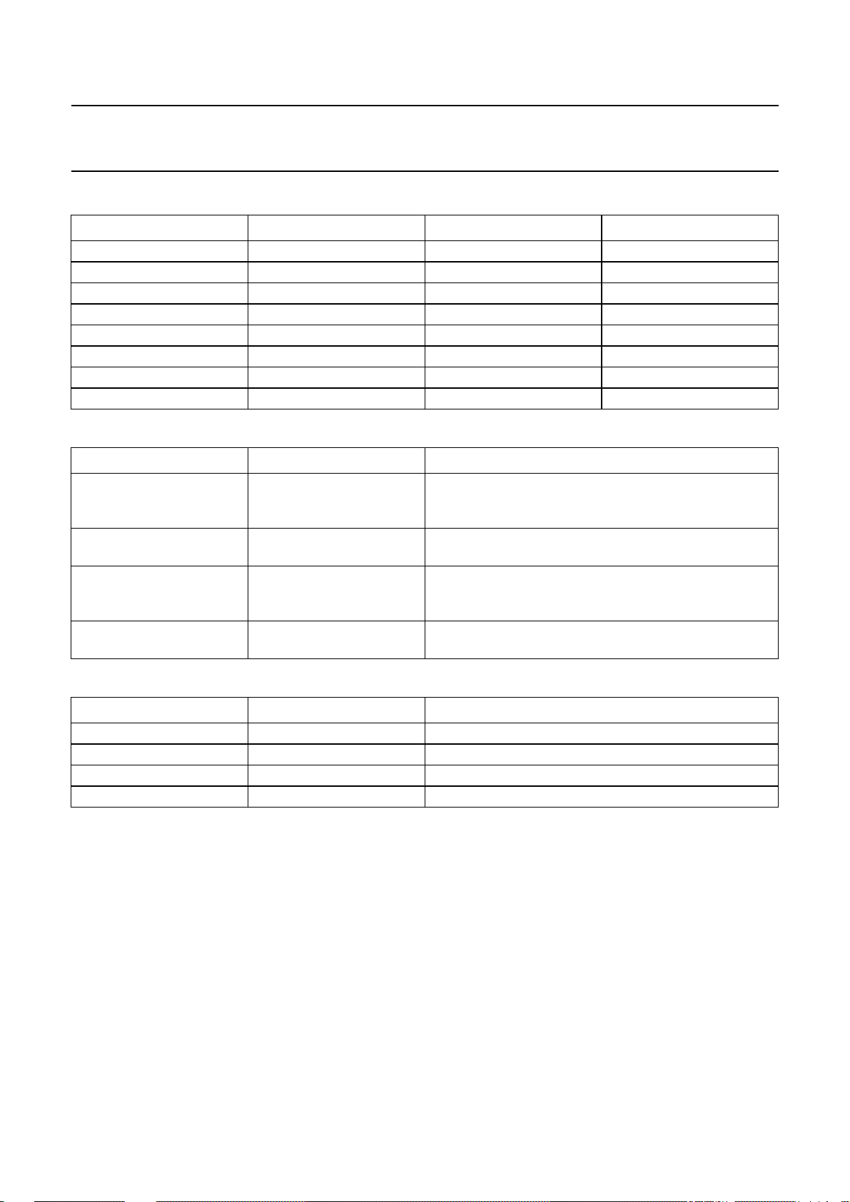
Table 12 Reference frequency setting
RFS2 RFS1 RFS0 f
000100
10050
01025
11020
00110
10110
01110
11110
Table 13 FM mode
BND1 BND0 SELECTION
0 0 FM standard: dead zone high current charge pump active,
0 1 FM local: dead zone high current charge pump active,
1 0 FM East Europe: dead zone high current charge pump
1 1 FM weather band: N1 divider set to 1 and I and Q phase
(kHz)
ref
FM AGC defined by RF level and threshold level setting
by I2C-bus
FM AGC source current set to maximum
switched off, current of low current charge pump set
to 1 mA
shift network switched on, WX flag signal activated
Table 14 AM mode; note 1
BND1 BND0 SELECTION
0 0 AM mono; N2 divider set to 5 (SW)
0 1 AM stereo; N2 divider set to 5 (SW)
1 0 AM mono; N2 divider set to 10 (LW, MW)
1 1 AM stereo; N2 divider set to 10 (LW, MW)
Note
1. In AM mode dead zone high current charge pump switched off, current of low current charge pump set to 1 mA.
2001 Mar 08 31
Page 32
Philips Semiconductors Product specification
New In Car Entertainment (NICE) car radio TEA6840H
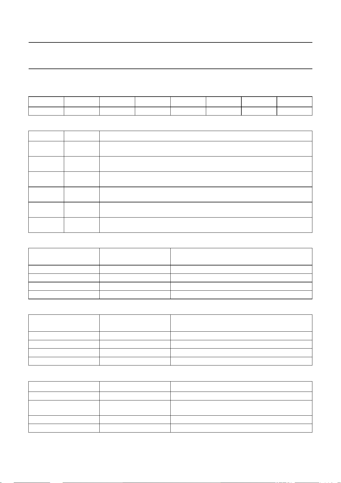
12.2.6 WRITE MODE: DATA BYTE 5
Table 15 Format of data byte 5
BIT 7 BIT 6 BIT 5 BIT 4 BIT 3 BIT 2 BIT 1 BIT 0
KAGC WBA1 WBA0 AMSM TMS3 TMS2 TMS1 TMS0
Table 16 Description of data byte 5 bits
BIT SYMBOL DESCRIPTION
7KAGCKeyed FM AGC. If KAGC = 0, then keyed FM AGC is off. If KAGC = 1, then keyed
FM AGC is on.
6 and 5 WBA[1:0] Wide band AGC. These 2 bits set the start value of wide band AGC. For AM,
see Table 17 and for FM, see Table 18.
4 AMSM AM soft mute. If AMSM = 0, then AM soft mute is off. If AMSM = 1, then AM soft mute
is on.
3 TMS3 In test mode charge pump 3-state. If TMS3 = 0, then 3-state off. If TMS3 = 1, then
3-state on.
2 TMS2 In test mode external clock for level and antenna DAA. If TMS2= 0, then external
clock disabled. If TMS2 = 1, then external clock enabled.
1 and 0 TMS[1:0] In test mode setting of pin f
see Table 19.
. These 2 bits define the function of pin f
ref
ref
,
Table 17 Setting of wide band AGC for AM
WBA1 WBA0
0 0 375
0 1 500
1 0 625
1 1 750
Table 18 Setting of wide band AGC for FM
WBA1 WBA0
11 4
10 8
01 12
00 16
Table 19 Setting function of pin f
in test mode
ref
TMS1 TMS0 OUTPUT AT PIN f
0 0 reference frequency of TEA6880H or TEF6890H
0 1 tuner oscillator frequency divided by division ratio of
1 0 PLL synthesizer reference frequency
1 1 not used (no output)
AM MIXER 1 INPUT VOLTAGE (PEAK VALUE)
(mV)
FM RF MIXER INPUT VOLTAGE (RMS VALUE)
(mV)
ref
programmable divider
2001 Mar 08 32
Page 33
Philips Semiconductors Product specification
New In Car Entertainment (NICE) car radio TEA6840H
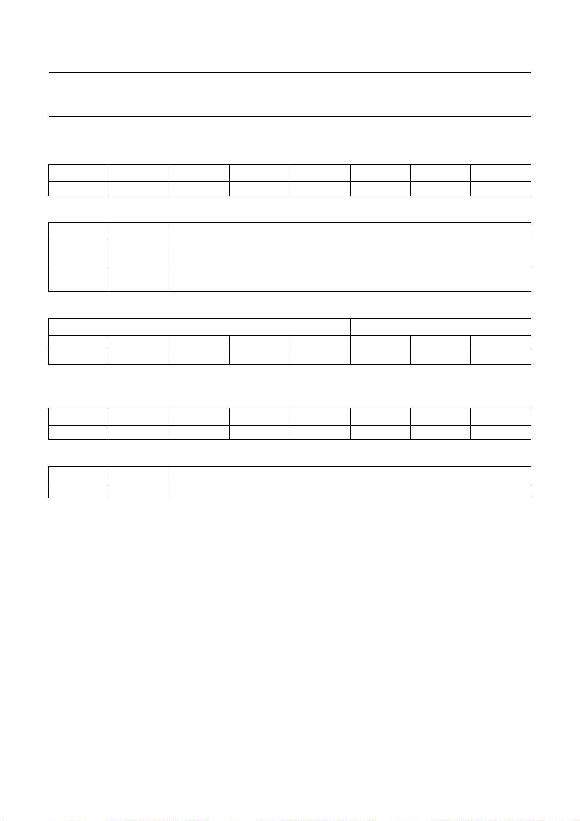
12.2.7 WRITE MODE: DATA BYTE 6
Table 20 Format of data byte 6
BIT 7 BIT 6 BIT 5 BIT 4 BIT 3 BIT 2 BIT 1 BIT 0
LST4 LST3 LST2 LST1 LST0 LSL2 LSL1 LSL0
Table 21 Description of data byte 6 bits
BIT SYMBOL DESCRIPTION
7 to 3 LST[4:0] Setting of level DAA starting point. These 5 bits determine the offset of the level
detector output voltage.
2 to 0 LSL[2:0] Setting of level DAA slope. These 3 bits determine the steepness of the leveldetector
output voltage.
Table 22 Standard setting of data byte 6 bits
SETTING OF LEVEL DAA STARTING POINT SETTING OF LEVEL DAA SLOPE
LST4 LST3 LST2 LST1 LST0 LSL2 LSL1 LSL0
10000100
12.2.8 READ MODE: DATA BYTE 1
Table 23 Format of 1st data byte
BIT 7 BIT 6 BIT 5 BIT 4 BIT 3 BIT 2 BIT 1 BIT 0
IFC7 IFC6 IFC5 IFC4 IFC3 IFC2 IFC1 IFC0
Table 24 Description of data byte 1 bits
BIT SYMBOL DESCRIPTION
7 to 0 IFC[7:0] IF counter result. These bits contain the last eight bits of the IF counter result.
2001 Mar 08 33
Page 34
Philips Semiconductors Product specification
New In Car Entertainment (NICE) car radio TEA6840H
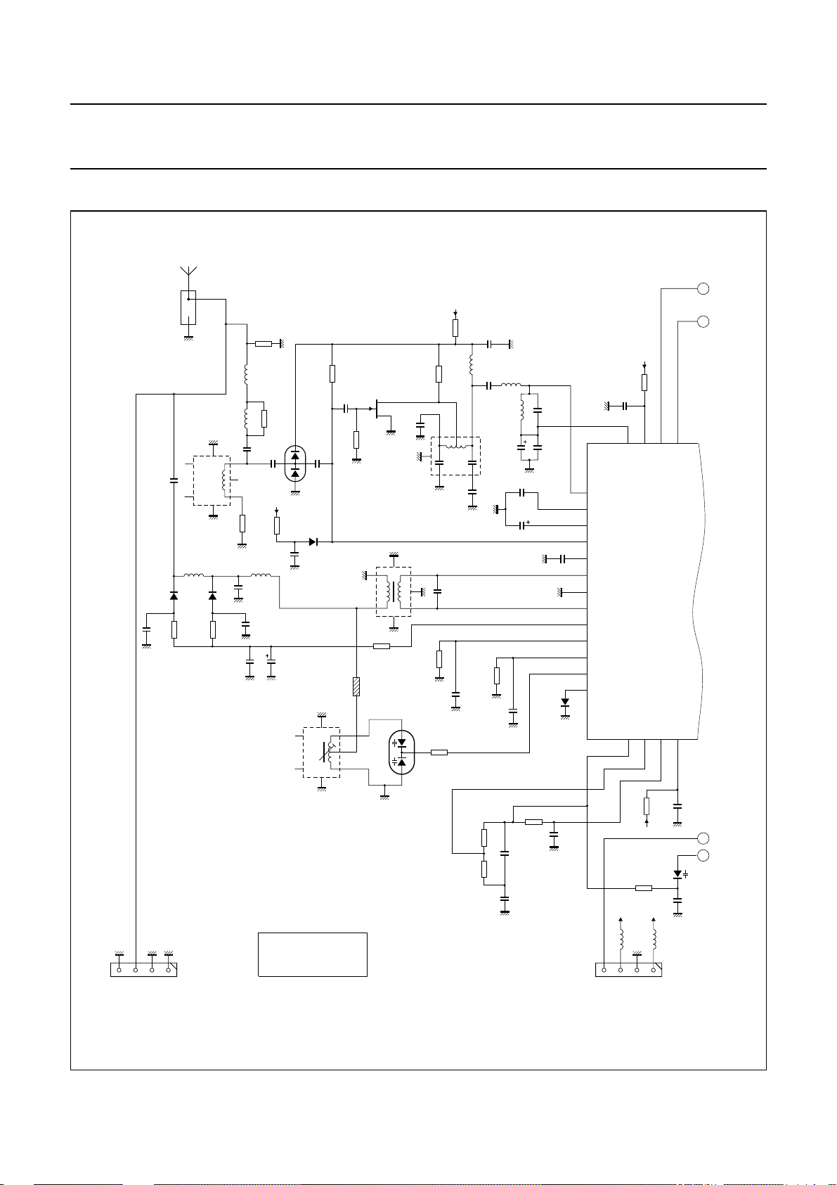
13 TEST AND APPLICATION INFORMATION
handbook, full pagewidth
C27
15 pF
BA595
C64
1 nF
ANT
GND
GND
P6
AERIAL_CON
MIX1OUT1
MIX1OUT2
DDA4
CPOUT
V
D7
C56
270 pF
P2
A
B
C
D
ANT
R3
2.2 MΩ
5 V
C36
10 µF
(25 V)
TOKO
1.8 MΩ
D1
BAV99
BAQ806
C30
100 nF
4
6
R11
C23
470
pF
D2
L11
TOKO
396INS_3076X
8
L17
7
C14
1 nF
3
2
1
TR1
BF861C
D
G
S
R15
2.2 MΩ
H285LCIS-13470
4
6
R20
22 Ω
SL1
SLINE.a
D6
BB814
C24
0.47
8
7
L2
3.3 µH
L9
6.8 µH
L16
7
6
7PD
8RBS
10RBM
4
8
10 kΩ
L12
290 nH
D4
D3
BA595
R52
R51
2.2 kΩ
330 Ω
P1
GND
R14
560 Ω
C22
1
C33
nF
1
10 nF
2
3
+
R8
R18
270 Ω
L13
290 nH
C69
15 pF
C65
1 nF
C35
1 nF
611SNS-1066Y
FM : 87.5 to 108 MHz
AM - MW : 520 to 12620 kHz
AM - LW : 153 to 279 kHz
AM - SW (49 m) : 5.9 to 6.2 MHz
1.5 kΩ
pF
L10
3
2
1
1 MΩ
+
8.5 V
1 mH
R5
2
1
7
46
C63
150 pF
C31
8.2 pF
R22
C38
1 µF
R28
22 kΩ
R2
47 Ω
L3
3
XR_0805
R37
2.2 kΩ
R39
1.2 kΩ
MHB885
C3
22 nF
C6
1.5 nF
R23
L5
18 µH
L8
820 µH
C20
47 µF
(16 V)
220 nF
22 µF (16 V)
C39
1 µF
C25
C26
C55
3.9 nF
C58
100 nF
R31
10 kΩ
C11
47 pF
C21
100 nF
BAS16
D5
C29
22 nF
C53
3.3 nF
32
31
30
29
28
27
26
25
24
23
22
21
20
C12
22 nF
AMMIX1IN1
T1AMAGC
T2AMAGC
IAMAGC
V
ref(FMMIX)
FMMIXIN2
RFGND
FMMIXIN1
IFMAGC
T2FMAGC
T1FMAGC
DAAOUT
DAATD
+
8.5 V
F_ref
+
8.5 V
R9
22 Ω
33 34 35 36
DDA5
V
AMMIX1IN2
TEA6840H
tune
DAAIN
V
19 18 17 16
R32
C50
22 Ω
22 nF
+
8.5 V
BB156
R40
4.7 kΩ
+
5 V
L20
L19
1 µH
3.3 µH
5 V
GND
8.5 V
Fig.7 Application diagram (continued in Fig.8).
2001 Mar 08 34
Page 35
Philips Semiconductors Product specification
New In Car Entertainment (NICE) car radio TEA6840H
handbook, full pagewidth
+
8.5 V
A
B
C
D
R1
22 Ω
C1
L1
TOKO
22 pF
P7PSG-X398
7
1
2
3
8
+
8.5 V
C9
R7
22
22
nF
Ω
C15
22
nF
37 38 39 40 41 42 43 44 45 46 47 48 49 50 51
DDA6
V
IFAMP1DEC
6
4
IFAMP1IN
IFAMP1OUT
SFE10.7MS3A10K-A
FL1
31
offset
C
C10
220 nF
FL2
2
1
IF1GND
IFAMP2IN
2
C16
22
nF
IFAMP2DEC
3
AMIF2IN
3
5
C8
22
nF
42
FL3
CFWS450HT
1
+
5 V
AMNBHOLD
IFAMP2OUT
FL5
2
1
C17
22
nF
FMLIMIN
AMIF2DEC
TEA6840H
DDD
ref
f
V
VCOGND
DGND
151413121110987654321
C45
100 nF
+
5 V
E543SNAS_02010
TOKO
7
L18
OSCFDB
OSCTNK
C43
2.7
pF
C46
4
8
1
C61
22 nF
DDA3
V
AFSAMPLE
1.8
pF
R43
22 Ω
AFHOLD
+
C62
47 µF
(16 V)
TRDSMUTE
C40
6.8
nF
R36
0 Ω
8.5 V
AMAFIF2
RDSMPX
FMMPX
SFE10.7MS3A10K-A
3
R10
330 Ω
C13
22 nF
AGC
C
FMLIMDEC
AMMIX2OUT1
AMMIX2OUT2
XTAL1
XTALGND
XTAL2
V
C
QDET1
QDET2
IF2GND
DDA1
DDA2
V
V
C41
100 nF
C47
100 nF
C51
R33
0 Ω
100 nF
level
AFC
SCL
SDA
3
8
C7
10 µF
(16 V)
52
53
54
I
ref
55
56
57
58
59
47 µF (16 V)
60
61
62
63
64
C42
47 µF
(16 V)
C48
47 µF
(16 V)
C52
100 nF
R50
0 Ω
C32
+
+
8.5 V
5 V
456
X1
20.5 MHz
LEVEL
RDS_MPX
R26
330 Ω
SDA
R21
4.7 kΩ
P7PSGAE-5078D=S
TOKO
7
R12
22 Ω
C18
22 nF
R16 120 kΩ
C28 220 nF
P293BC-1977Z
L15
1
2
3
R24
330 Ω
NC
SCL
MPX
MHB886
7
8
AM_AF
6
TOKO
4
GND
+
8.5 V
AFSAMPLE
AFSAMPLE
+
5 V
P3
L6
1
2
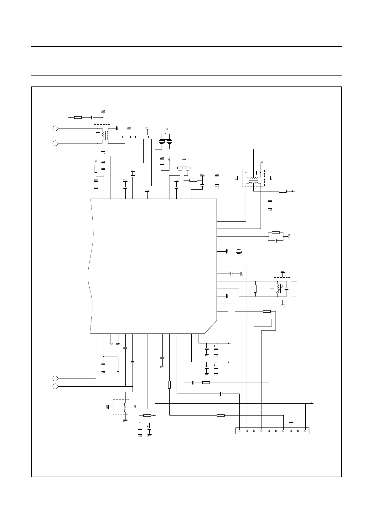
Fig.8 Application diagram (continued from Fig.7).
2001 Mar 08 35
Page 36
Philips Semiconductors Product specification
New In Car Entertainment (NICE) car radio TEA6840H
handbook, full pagewidth
WB
FLAG
antenna
input
470
kΩ
f
22 Ω
16 1314
WX
N1
÷2
90°
AM NOISE
DETECTOR
N2
÷5/10
ref
22
nF
SFE10.7
MS3
PLL
A
B
C
100
nF
3.3
DGND
µH
100 nF
15
10.25 MHz
PEAK/
AVERAGE
IFAMP1
304 Ω
D
E
F
G
H
I
J
K
L
M
N
O
P
Q
R
S
FM RF input
V
tune
10 kΩ
2.2 kΩ
50 Ω
19
ANTENNA
FM
AGC
AM
RF AGC
100
DAA
nF
3.9
nF
1.2 kΩ
100 nF
FM
I/Q MIXER
90°
×
AM
MIXER1
33 34
relay 2
AM
×
22 Ω
TEA6840H
22
nF
47 Ω
100 nF
relay 1
teledyne
1 µF
4:7
L5
RFGND
22 nF
180
pF
20
21
22
23
24
25
26
27
28
29
30
31
32
4.7 µF
100 nF
t
BAQ800
BA595
BA595
100 nF
100
pF
22 kΩ
120
nH
(1)
330 pF
1 nF470 pF
560 pF
3.3 µH
1.5 to
100
5 pF
nF
1 MΩ
22 Ω
47 µF
680
100
µH
µH
1 nF
1.2 MΩ
BF861C
470
kΩ
V
BB814
8.2
270
270
47 Ω
pF
L6
470 nH
47 pF
8.2
pF
L7
220 nH
Ω
100 nF
Ω
220
nF
1 mH
220 µH
1.5 kΩ
BAV99
1 nF
6.8
µH
relay 1
22
nF
17
18
TUNING SYSTEM
37 38 39
35 36
22
nF
L1
22 nF
22 Ω 10 Ω
3.3
nF
100 nF 100 nF
AM RF
input
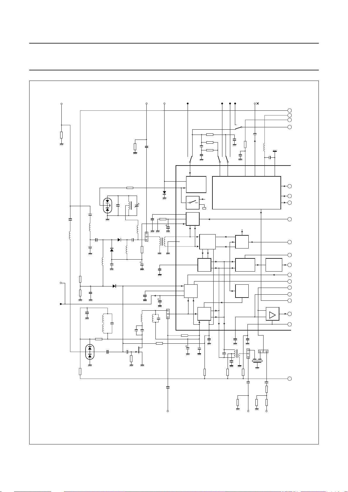
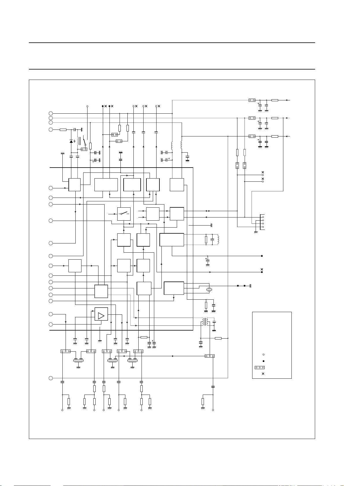
Fig.9 Test circuit (continued in Fig.10).
2001 Mar 08 36
330 Ω
output
52 Ω 2 Ω
IF
IF
input
MHB488
Page 37
Philips Semiconductors Product specification
New In Car Entertainment (NICE) car radio TEA6840H
handbook, full pagewidth
A
B
C
4.7 kΩ
D
BB156
E
F
G
H
I
J
K
L
M
N
O
P
Q
R
S
FM
RDS/
68
kΩ68 kΩ
IF AGC
LEVEL
100 nF100 nF
AUDIO/IF
10 nF
DETECTOR
AM
AM
SFE10.7
MS3
AM
100
nF
AM
FM IF
AM IF2
MPX
LEVEL
DAA
100
nF
MUTE
IF
COUNT
MPX
Σ
FM
LIMITER/
LEVEL
51
330 Ω
100
nF
100
nF
100 nF
304 Ω
AF
AF
SAMPLE
HOLD
(1)
270 pF
L8
22 Ω
MS3
22 nF
1.8
pF
47 µF
10 9 345612
220
nF
100 nF
304 Ω
8
SEQUENTIAL
CIRCUIT FOR
RDS UPDATING
I2C-bus
×
AM
MIXER2
IFAMP2
100
IF1GND
2 kΩ
7
nF
SFR
450H
2.7
pF
11 2
VCO
BLANK
PULSE
40 41 42 4543 44 46 50494847
22
nF
SFE10.7
100 nF
100
nF
3.3 µH
100 nF
47 µF
2 ms/
20 ms
DEMODULATOR
CRYSTAL
OSCILLATOR
TEA6840H
10 µF
POWER
SUPPLY
I2C-BUS
3.3 µH
1
100 nF
64
63
62
61
60
59
58
57
56
55
54
53
52
SDA
SCL
IF2GND
22 nF
10 Ω
47 µF
47 µF
47 µF
39
39
kΩ
kΩ
4.7
kΩ
120
kΩ
L3
4.7 µF
20.5
MHz
220
nF
L2
22 Ω
100 nF
wire
100 nF
10 Ω
100 nF
10 Ω
100 nF
SDA
SCL
2
I
C-bus
interface
DGND
AFC
AM/FM
LEVEL
Coils:
L1: P392BE-2104GNL = S
L2: P7PSAE-2119D = S
L3: 392BC-1977Z
L4: 611SNS-1066Y
L5: 396INS-3076X
L6: MURATA LQN
L7: MURATA LQN
L8: air coil 2 turns, 30 nH
(1): series NP0
coaxial connector
test pin
jumper
to TEA6880H
5 V
analog
5 V
digital
8.5 V
FM IF1
output
330 Ω
52 Ω 2 Ω
FM IF2
input
AM IF2
input
47 Ω
FM IF2
output
330 Ω
limiter
input
52 Ω2 Ω
Fig.10 Test circuit (continued from Fig.9).
2001 Mar 08 37
2 kΩ
AM IF
output
MHB489
Page 38
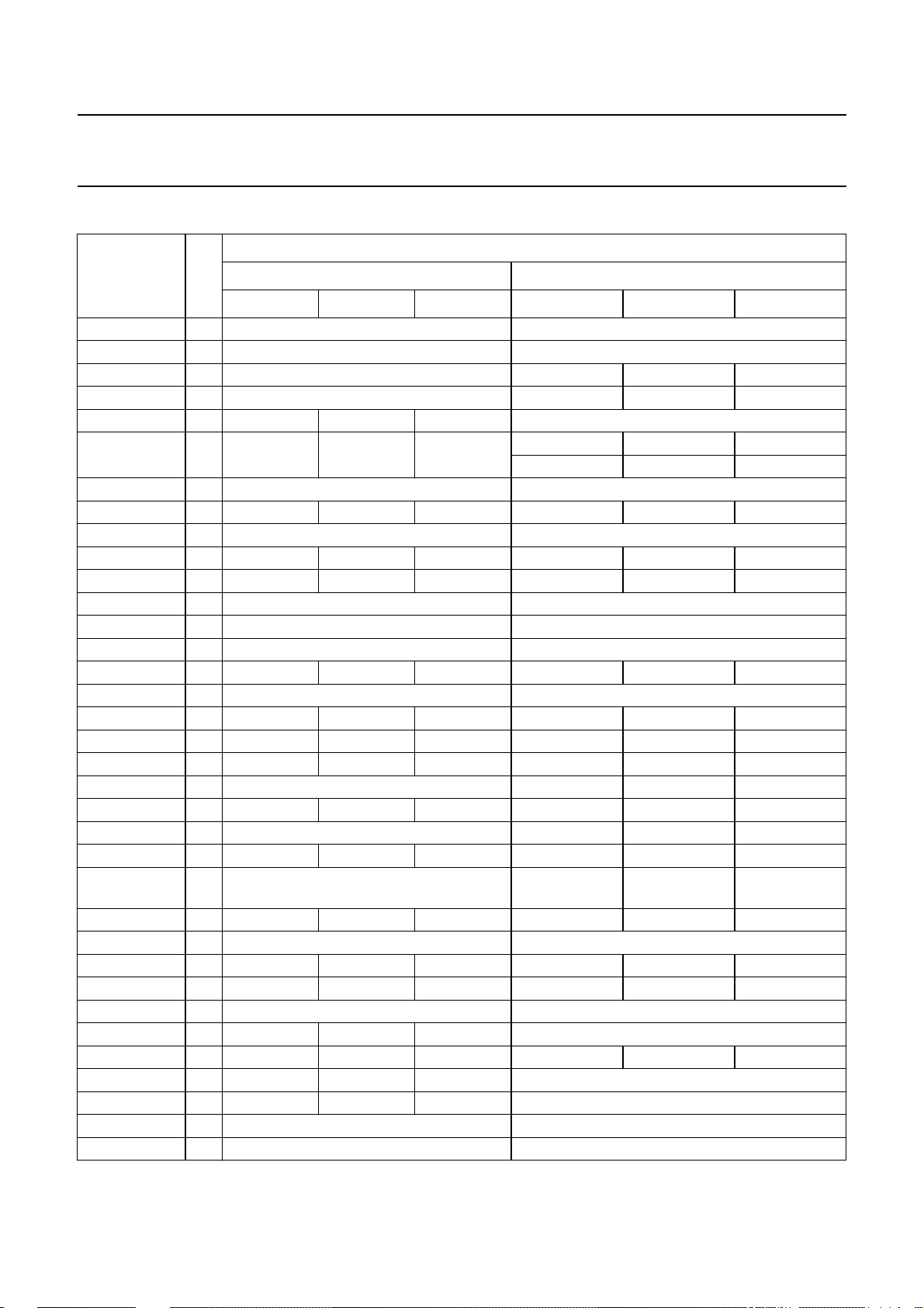
Philips Semiconductors Product specification
New In Car Entertainment (NICE) car radio TEA6840H
Table 25 DC operating points
UNLOADED DC VOLTAGE (V)
SYMBOL PIN
AM MODE FM MODE
MIN. TYP. MAX. MIN. TYP. MAX.
V
V
DDA1
DDA2
1 external 8.5 external 8.5
2 external 5 external 5
FMMPX 3 floating 3 3.5 4
RDSMPX 4 floating 2.6 3.1 3.3
AMAFIF2 5 4 4.3 4.6 floating
TRDSMUTE 6 1.9 2.2 2.5 0.7 (muted) 1.2 (muted) 1.7 (muted)
5.2 (not muted) 5.7 (not muted) 6.2 (not muted)
AFHOLD 7 open-collector open-collector
AFSAMPLE 8 0 0.2 0.5 0 0.2 0.5
V
DDA3
9 external 8.5 external 8.5
OSCTNK 10 5 6.1 7.2 5 6.1 7.2
OSCFDB 11 2.2 2.8 3.4 2.2 2.8 3.4
VCOGND 12 external 0 external 0
DGND 13 external 0 external 0
V
f
ref
V
DDD
DDA4
14 external 5 external 5
15 3.2 3.4 3.7 3.2 3.4 3.7
16 external 8.5 external 8.5
CPOUT 17 0 − 8.5 0 − 8.5
V
tune
18 0 − 8.5 0 − 8.5
DAAIN 19 0 − 8.5 0 − 8.5
DAATD 20 floating 0.2 − 1.5
DAAOUT 21 − 0.2 0.3 0.2 − 8.25
T1FMAGC 22 floating 1 − 7
T2FMAGC 23 7.5 8 8.3 3.9 4.6 5.3
IFMAGC 24 floating 1.5 (external
biasing)
− 4 (external
biasing)
FMMIXIN1 25 1 1.3 1.6 2.3 2.8 3.3
RFGND 26 external 0 external 0
FMMIXIN2 27 1 1.3 1.6 2.3 2.8 3.3
V
ref(FMMIX)
28 2.7 3.1 3.4 6.5 7.1 7.9
IAMAGC 29 open-collector open-collector
T2AMAGC 30 2.5 2.8 3.1 floating
T1AMAGC 31 0 2.8 4.6 0 (no WX) 0.3 (no WX) 0.5 (no WX)
AMMIX1IN1 32 2.3 2.75 3.1 floating
AMMIX1IN2 33 2.3 2.75 3.1 floating
V
DDA5
34 external 8.5 external 8.5
MIX1OUT1 35 external 8.5 external 8.5
2001 Mar 08 38
Page 39
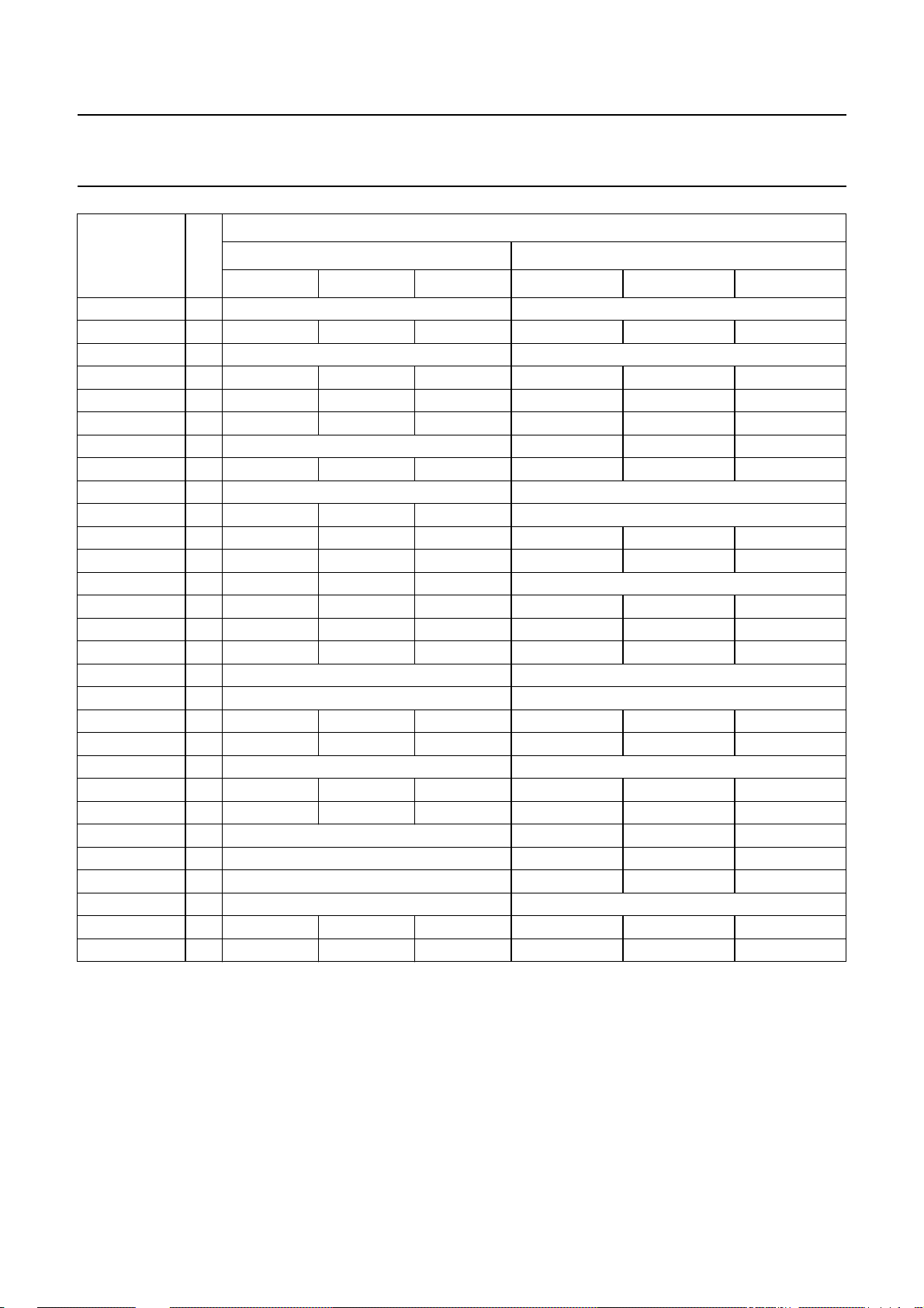
Philips Semiconductors Product specification
New In Car Entertainment (NICE) car radio TEA6840H
UNLOADED DC VOLTAGE (V)
SYMBOL PIN
AM MODE FM MODE
MIN. TYP. MAX. MIN. TYP. MAX.
MIX1OUT2 36 external 8.5 external 8.5
IFAMP1DEC 37 2.4 2.7 3 2.3 2.7 3.1
V
DDA6
38 external 8.5 external 8.5
IFAMP1IN 39 2.4 2.7 3 2.3 2.7 3.1
IFAMP1OUT 40 7.2 7.9 − 3.6 4 4.4
IFAMP2DEC 41 3 4 5 2.7 3.1 3.5
C
offset
42 floating 3 3.5 4
IFAMP2IN 43 3 4 5 2.7 3.1 3.5
IF1GND 44 external 0 external 0
AMIF2IN 45 2.4 2.7 3.2 floating
AMNBHOLD 46 4.3 4.6 5.1 8 8.4 −
IFAMP2OUT 47 7.2 7.9 − 3.4 3.9 4.4
AMIF2DEC 48 2.4 2.7 3.2 floating
FMLIMIN 49 2.5 3 3.5 2.5 2.8 3.1
FMLIMDEC 50 2.5 3 3.5 2.5 2.8 3.1
C
AGC
51 3.6 4.3 4.8 4.1 4.6 5.1
AMMIX2OUT1 52 external 8.5 external 8.5
AMMIX2OUT2 53 external 8.5 external 8.5
I
ref
54 4 4.25 4.5 4 4.25 4.5
XTAL1 55 1.7 2.1 2.5 1.7 2.1 2.5
XTALGND 56 external 0 external 0
XTAL2 57 1.7 2.1 2.5 1.7 2.1 2.5
V
C
level
AFC
58 0.05 − 70 − 7
59 floating 1.2 3.4 4.1
QDET1 60 floating 3.6 4.1 4.6
QDET2 61 floating 3.6 4.1 4.6
IF2GND 62 external 0 external 0
SCL 63 4.8 5 5.2 4.8 5 5.2
SDA 64 4.8 5 5.2 4.8 5 5.2
2001 Mar 08 39
Page 40
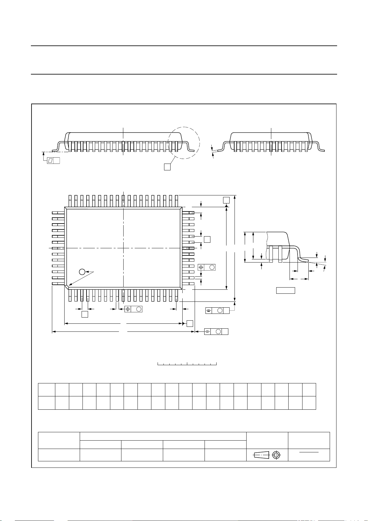
Philips Semiconductors Product specification
New In Car Entertainment (NICE) car radio TEA6840H
14 PACKAGE OUTLINE
QFP64: plastic quad flat package; 64 leads (lead length 1.95 mm); body 14 x 20 x 2.8 mm
c
y
X
SOT319-2
51 33
52
pin 1 index
64
1
w M
b
e
p
Z
D
D
H
D
0 5 10 mm
DIMENSIONS (mm are the original dimensions)
mm
A
max.
3.20
0.25
0.05
2.90
2.65
0.25
0.50
0.35
0.25
0.14
UNIT A1A2A3bpcE
(1)
(1) (1)(1)
D
20.1
14.1
19.9
13.9
32
Z
E
e
w M
b
p
20
19
v M
B
v M
scale
eH
H
D
24.2
1
23.6
18.2
17.6
E
LL
E
A
B
1.0
0.6
A
A
H
E
2
A
A
1
(A )
3
θ
L
p
L
detail X
Zywv θ
p
0.2 0.10.21.95
Z
E
D
1.2
0.8
o
7
o
0
1.2
0.8
Note
1. Plastic or metal protrusions of 0.25 mm maximum per side are not included.
OUTLINE
VERSION
IEC JEDEC EIAJ
REFERENCES
SOT319-2 MO-112
2001 Mar 08 40
EUROPEAN
PROJECTION
ISSUE DATE
97-08-01
99-12-27
Page 41

Philips Semiconductors Product specification
New In Car Entertainment (NICE) car radio TEA6840H
15 SOLDERING
15.1 Introduction to soldering surface mount packages
Thistextgivesaverybriefinsighttoacomplextechnology.
A more in-depth account of soldering ICs can be found in
our
“Data Handbook IC26; Integrated Circuit Packages”
(document order number 9398 652 90011).
There is no soldering method that is ideal for all surface
mount IC packages. Wave soldering can still be used for
certainsurfacemountICs,butitisnotsuitable for fine pitch
SMDs. In these situations reflow soldering is
recommended.
15.2 Reflow soldering
Reflow soldering requires solder paste (a suspension of
fine solder particles, flux and binding agent) to be applied
totheprinted-circuitboardby screen printing, stencilling or
pressure-syringe dispensing before package placement.
Several methods exist for reflowing; for example,
convection or convection/infrared heating in a conveyor
type oven. Throughput times (preheating, soldering and
cooling) vary between 100 and 200 seconds depending
on heating method.
Typical reflow peak temperatures range from
215 to 250 °C. The top-surface temperature of the
packages should preferable be kept below 220 °C for
thick/large packages, and below 235 °C for small/thin
packages.
15.3 Wave soldering
Conventional single wave soldering is not recommended
forsurfacemountdevices(SMDs)orprinted-circuitboards
with a high component density, as solder bridging and
non-wetting can present major problems.
To overcome these problems the double-wave soldering
method was specifically developed.
If wave soldering is used the following conditions must be
observed for optimal results:
• Use a double-wave soldering method comprising a
turbulent wave with high upward pressure followed by a
smooth laminar wave.
• For packages with leads on two sides and a pitch (e):
– larger than or equal to 1.27 mm, the footprint
longitudinal axis is preferred to be parallel to the
transport direction of the printed-circuit board;
– smaller than 1.27 mm, the footprint longitudinal axis
must be parallel to the transport direction of the
printed-circuit board.
The footprint must incorporate solder thieves at the
downstream end.
• Forpackageswithleadsonfoursides,thefootprint must
be placed at a 45° angle to the transport direction of the
printed-circuit board. The footprint must incorporate
solder thieves downstream and at the side corners.
During placement and before soldering, the package must
be fixed with a droplet of adhesive. The adhesive can be
applied by screen printing, pin transfer or syringe
dispensing. The package can be soldered after the
adhesive is cured.
Typical dwell time is 4 seconds at 250 °C.
A mildly-activated flux will eliminate the need for removal
of corrosive residues in most applications.
15.4 Manual soldering
Fix the component by first soldering two
diagonally-opposite end leads. Use a low voltage (24 V or
less) soldering iron applied to the flat part of the lead.
Contact time must be limited to 10 seconds at up to
300 °C.
When using a dedicated tool, all other leads can be
soldered in one operation within 2 to 5 seconds between
270 and 320 °C.
2001 Mar 08 41
Page 42

Philips Semiconductors Product specification
New In Car Entertainment (NICE) car radio TEA6840H
15.5 Suitability of surface mount IC packages for wave and reflow soldering methods
PACKAGE
WAVE REFLOW
(1)
BGA, LFBGA, SQFP, TFBGA not suitable suitable
SOLDERING METHOD
HBCC, HLQFP, HSQFP, HSOP, HTQFP, HTSSOP, SMS not suitable
(3)
PLCC
, SO, SOJ suitable suitable
LQFP, QFP, TQFP not recommended
SSOP, TSSOP, VSO not recommended
(2)
(3)(4)
(5)
suitable
suitable
suitable
Notes
1. All surface mount (SMD) packages are moisture sensitive. Depending upon the moisture content, the maximum
temperature (with respect to time) and body size of the package, there is a risk that internal or external package
cracks may occur due to vaporization of the moisture in them (the so called popcorn effect). For details, refer to the
Drypack information in the
“Data Handbook IC26; Integrated Circuit Packages; Section: Packing Methods”
.
2. These packages are not suitable for wave soldering as a solder joint between the printed-circuit board and heatsink
(at bottom version) can not be achieved, and as solder may stick to the heatsink (on top version).
3. If wave soldering is considered, then the package must be placed at a 45° angle to the solder wave direction.
The package footprint must incorporate solder thieves downstream and at the side corners.
4. Wave soldering is only suitable for LQFP, TQFP and QFP packages with a pitch (e) equal to or larger than 0.8 mm;
it is definitely not suitable for packages with a pitch (e) equal to or smaller than 0.65 mm.
5. Wave soldering is only suitable for SSOP and TSSOP packages with a pitch (e) equal to or larger than 0.65 mm; it is
definitely not suitable for packages with a pitch (e) equal to or smaller than 0.5 mm.
2001 Mar 08 42
Page 43

Philips Semiconductors Product specification
New In Car Entertainment (NICE) car radio TEA6840H
16 DATA SHEET STATUS
DATA SHEET STATUS
PRODUCT
STATUS
DEFINITIONS
(1)
Objective specification Development This data sheet contains the design target or goal specifications for
product development. Specification may change in any manner without
notice.
Preliminary specification Qualification This data sheet contains preliminary data, and supplementary data will be
published at a later date. Philips Semiconductors reserves the right to
make changes at any time without notice in order to improve design and
supply the best possible product.
Product specification Production This data sheet contains final specifications. Philips Semiconductors
reserves the right to make changes at any time without notice in order to
improve design and supply the best possible product.
Note
1. Please consult the most recently issued data sheet before initiating or completing a design.
17 DEFINITIONS
Short-form specification The data in a short-form
specification is extracted from a full data sheet with the
same type number and title. For detailed information see
the relevant data sheet or data handbook.
Limiting values definition Limiting values given are in
accordance with the Absolute Maximum Rating System
(IEC 60134). Stress above one or more of the limiting
values may cause permanent damage to the device.
These are stress ratings only and operation of the device
attheseoratanyotherconditionsabovethosegiveninthe
Characteristics sections of the specification is not implied.
Exposure to limiting values for extended periods may
affect device reliability.
Application information Applications that are
described herein for any of these products are for
illustrative purposes only. Philips Semiconductors make
norepresentationorwarrantythatsuchapplications will be
suitable for the specified use without further testing or
modification.
18 DISCLAIMERS Life support applications These products are not
designed for use in life support appliances, devices, or
systems where malfunction of these products can
reasonably be expected to result in personal injury. Philips
Semiconductorscustomersusingorsellingthese products
for use in such applications do so at their own risk and
agree to fully indemnify Philips Semiconductors for any
damages resulting from such application.
Right to make changes Philips Semiconductors
reserves the right to make changes, without notice, in the
products, including circuits, standard cells, and/or
software, described or contained herein in order to
improve design and/or performance. Philips
Semiconductors assumes no responsibility or liability for
theuseofanyoftheseproducts,conveysno licence or title
under any patent, copyright, or mask work right to these
products,andmakesnorepresentationsorwarrantiesthat
these products are free from patent, copyright, or mask
work right infringement, unless otherwise specified.
19 PURCHASE OF PHILIPS I
Purchase of Philips I
2
C COMPONENTS
2
C components conveys a license under the Philips’ I2C patent to use the
components in the I2C system provided the system conforms to the I2C specification defined by
Philips. This specification can be ordered using the code 9398 393 40011.
2001 Mar 08 43
Page 44

Philips Semiconductors – a w orldwide compan y
Argentina: see South America
Australia: 3 Figtree Drive, HOMEBUSH, NSW 2140,
Tel. +61 2 9704 8141, Fax. +61 2 9704 8139
Austria: Computerstr. 6, A-1101 WIEN, P.O. Box 213,
Tel. +43 1 60 101 1248, Fax. +43 1 60 101 1210
Belarus: Hotel Minsk Business Center, Bld. 3, r. 1211, Volodarski Str. 6,
220050 MINSK, Tel. +375 172 20 0733, Fax. +375 172 20 0773
Belgium: see The Netherlands
Brazil: see South America
Bulgaria: Philips Bulgaria Ltd., Energoproject, 15th floor,
51 James Bourchier Blvd., 1407 SOFIA,
Tel. +359 2 68 9211, Fax. +359 2 68 9102
Canada: PHILIPS SEMICONDUCTORS/COMPONENTS,
Tel. +1 800 234 7381, Fax. +1 800 943 0087
China/Hong Kong: 501 Hong Kong Industrial Technology Centre,
72 Tat Chee Avenue, Kowloon Tong, HONG KONG,
Tel. +852 2319 7888, Fax. +852 2319 7700
Colombia: see South America
Czech Republic: see Austria
Denmark: Sydhavnsgade 23, 1780 COPENHAGEN V,
Tel. +45 33 29 3333, Fax. +45 33 29 3905
Finland: Sinikalliontie 3, FIN-02630 ESPOO,
Tel. +358 9 615 800, Fax. +358 9 6158 0920
France: 7 - 9 Rue du Mont Valérien, BP317, 92156 SURESNES Cedex,
Tel. +33 1 4728 6600, Fax. +33 1 4728 6638
Germany: Hammerbrookstraße 69, D-20097 HAMBURG,
Tel. +49 40 2353 60, Fax. +49 40 2353 6300
Hungary: Philips Hungary Ltd., H-1119 Budapest, Fehervari ut 84/A,
Tel: +36 1 382 1700, Fax: +36 1 382 1800
India: Philips INDIA Ltd, Band Box Building, 2nd floor,
254-D, Dr. Annie Besant Road, Worli, MUMBAI 400 025,
Tel. +91 22 493 8541, Fax. +91 22 493 0966
Indonesia: PTPhilips DevelopmentCorporation, Semiconductors Division,
Gedung Philips, Jl. Buncit Raya Kav.99-100, JAKARTA 12510,
Tel. +62 21 794 0040 ext. 2501, Fax. +62 21 794 0080
Ireland: Newstead, Clonskeagh, DUBLIN 14,
Tel. +353 1 7640 000, Fax. +353 1 7640 200
Israel: RAPAC Electronics, 7 Kehilat Saloniki St, PO Box 18053,
TEL AVIV 61180, Tel. +972 3 645 0444, Fax. +972 3 649 1007
Italy: PHILIPS SEMICONDUCTORS,Via Casati, 23 - 20052 MONZA (MI),
Tel. +39 039 203 6838, Fax +39 039 203 6800
Japan: Philips Bldg 13-37, Kohnan 2-chome, Minato-ku,
TOKYO 108-8507, Tel. +81 3 3740 5130, Fax. +81 3 3740 5057
Korea: Philips House, 260-199 Itaewon-dong, Yongsan-ku, SEOUL,
Tel. +82 2 709 1412, Fax. +82 2 709 1415
Malaysia: No. 76 Jalan Universiti, 46200 PETALING JAYA, SELANGOR,
Tel. +60 3 750 5214, Fax. +60 3 757 4880
Mexico: 5900 Gateway East, Suite 200, EL PASO, TEXAS 79905,
Tel. +9-5 800 234 7381, Fax +9-5 800 943 0087
Middle East: see Italy
Netherlands: Postbus 90050, 5600 PB EINDHOVEN, Bldg. VB,
Tel. +31 40 27 82785, Fax. +31 40 27 88399
New Zealand: 2 Wagener Place, C.P.O. Box 1041, AUCKLAND,
Tel. +64 9 849 4160, Fax. +64 9 849 7811
Norway: Box 1, Manglerud 0612, OSLO,
Tel. +47 22 74 8000, Fax. +47 22 74 8341
Pakistan: see Singapore
Philippines: Philips Semiconductors Philippines Inc.,
106 Valero St. Salcedo Village, P.O. Box 2108 MCC, MAKATI,
Metro MANILA, Tel. +63 2 816 6380, Fax. +63 2 817 3474
Poland: Al.Jerozolimskie 195 B, 02-222 WARSAW,
Tel. +48 22 5710 000, Fax. +48 22 5710 001
Portugal: see Spain
Romania: see Italy
Russia: Philips Russia, Ul. Usatcheva 35A, 119048 MOSCOW,
Tel. +7 095 755 6918, Fax. +7 095 755 6919
Singapore: Lorong 1, Toa Payoh, SINGAPORE 319762,
Tel. +65 350 2538, Fax. +65 251 6500
Slovakia: see Austria
Slovenia: see Italy
South Africa: S.A. PHILIPS Pty Ltd., 195-215 Main Road Martindale,
2092 JOHANNESBURG, P.O. Box 58088 Newville 2114,
Tel. +27 11 471 5401, Fax. +27 11 471 5398
South America: Al. Vicente Pinzon, 173, 6th floor,
04547-130 SÃO PAULO, SP, Brazil,
Tel. +55 11 821 2333, Fax. +55 11 821 2382
Spain: Balmes 22, 08007 BARCELONA,
Tel. +34 93 301 6312, Fax. +34 93 301 4107
Sweden: Kottbygatan 7, Akalla, S-16485 STOCKHOLM,
Tel. +46 8 5985 2000, Fax. +46 8 5985 2745
Switzerland: Allmendstrasse 140, CH-8027 ZÜRICH,
Tel. +41 1 488 2741 Fax. +41 1 488 3263
Taiwan: Philips Semiconductors, 5F, No. 96, Chien Kuo N. Rd., Sec. 1,
TAIPEI, Taiwan Tel. +886 2 2134 2451, Fax. +886 2 2134 2874
Thailand: PHILIPS ELECTRONICS (THAILAND) Ltd.,
60/14 MOO 11, Bangna Trad Road KM. 3, Bagna, BANGKOK 10260,
Tel. +66 2 361 7910, Fax. +66 2 398 3447
Turkey: Yukari Dudullu, Org. San. Blg., 2.Cad. Nr. 28 81260 Umraniye,
ISTANBUL, Tel. +90 216 522 1500, Fax. +90 216 522 1813
Ukraine: PHILIPS UKRAINE, 4 Patrice Lumumba str., Building B, Floor 7,
252042 KIEV, Tel. +380 44 264 2776, Fax. +380 44 268 0461
United Kingdom: Philips Semiconductors Ltd., 276 Bath Road, Hayes,
MIDDLESEX UB3 5BX, Tel. +44 208 730 5000, Fax. +44 208 754 8421
United States: 811 East Arques Avenue, SUNNYVALE, CA 94088-3409,
Tel. +1 800 234 7381, Fax. +1 800 943 0087
Uruguay: see South America
Vietnam: see Singapore
Yugoslavia: PHILIPS, Trg N. Pasica 5/v, 11000 BEOGRAD,
Tel. +381 11 3341 299, Fax.+381 11 3342 553
For all other countries apply to: Philips Semiconductors,
Marketing Communications, Building BE-p, P.O. Box 218, 5600 MD EINDHOVEN,
The Netherlands, Fax. +31 40 27 24825
© Philips Electronics N.V. SCA
All rights are reserved. Reproduction in whole or in part is prohibited without the prior written consent of the copyright owner.
The information presented in this document does not form part of any quotation or contract, is believed to be accurate and reliable and may be changed
without notice. No liability will be accepted by the publisher for any consequence of its use. Publication thereof does not convey nor imply any license
under patent- or other industrial or intellectual property rights.
2001
Internet: http://www.semiconductors.philips.com
72
Printed in The Netherlands 753503/02/pp44 Date of release: 2001 Mar 08 Document order number: 9397 750 07618
 Loading...