

Page 1

INTEGRATED CIRCUITS
DATA SH EET
TEA5594
AM/FM radio receiver circuit
Product specification
File under Integrated Circuits, IC01
March 1991
Page 2

Philips Semiconductors Product specification
AM/FM radio receiver circuit TEA5594
GENERAL DESCRIPTION
The TEA5594 is a 32-pin integrated radio circuit designed
for use in all Electronic Tuned Radio (ETR) sets especially
those sets which have to fulfil the immunity requirements
of CENELEC.
The AM circuit incorporates:
• A double balanced mixer
• A ‘one-pin’ oscillator with amplitude control operating in
the LW/MW frequency range
• An IF amplifier and AM detector
• An AGC circuit which controls the IF amplifier and mixer
The FM circuit incorporates:
• A front-end (fulfilling the “out of band” CENELEC
requirements)
• Two IF amplifiers (for distributed selectivity)
• A quadrature demodulator with a ceramic filter
PACKAGE OUTLINE
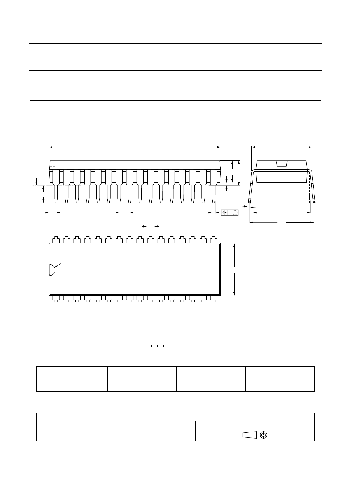
32-lead shrink DIL; plastic (SOT232); SOT232-1; 1996 September 9.
The TEA5594 also contains:
• Oscillator output buffers for AM and FM
• A combined AM/FM IF counter output buffer with
counter “enable” function
• A field strength level detector for AM and FM
• A soft mute circuit at FM, adjustable
• An extra IF amplifier to split up IF filtering
Features
• Low distortion on FM
• AM/FM level/indicator circuit
• A DC AM/FM switch facility
• Supply voltages 2.7 to 15 V
• A local distance switch facility (LOCAL-DX) at FM
• All pins are ESD protected
March 1991 2
Page 3

Philips Semiconductors Product specification
AM/FM radio receiver circuit TEA5594
QUICK REFERENCE DATA
PARAMETER CONDITIONS SYMBOL MIN. TYP. MAX. UNIT
Supply voltage (pin 9) V
P
Total current consumption
AM part I
FM part I
Operating ambient temperature range T
AM performance (pin 22)
Sensitivity V
note 1
= 10 mV V
o
(S + N)/N = 26 dB V
Signal-to-noise ratio V
= 1 mV (S + N)/N − 48 − dB
i
AF output voltage V
P
P
amb
i
i
o
Total harmonic distortion THD − 0.8 − %
Signal handling m = 80%; THD = 8% V
FM performance (pin 30)
note 2
Limiting sensitivity −3 dB; note 3 V
Signal-to-noise ratio V
= 3 µV (S + N)/N − 26 − dB
i
= 1 mV (S + N)/N − 60 − dB
V
i
AF output voltage V
i
i
o
Total harmonic distortion THD − 0.1 − %
Maximum signal handling V
AM suppression 100 µV < V
<
i
i
100 mV AMS − 50 − dB
2.7 − 15 V
− 13 − mA
− 24 − mA
−40 − +85 °C
− 3.5 −µV
− 16 −µV
− 50 − mV
− 100 − mV
− 2.5 −µV
− 90 − mV
− 200 − mV
Notes to the quick reference data
1. All parameters are measured in the application circuit (see Fig.5) at nominal supply voltage V
unless otherwise specified. RF conditions: Input frequency 1 MHz; 30% modulated with f
= 8.5 V; T
p
= 1 kHz; unless
mod
otherwise specified.
2. All parameters are measured in the application circuit (see Fig.5) at nominal supply voltage Vp = 8.5 V; T
unless otherwise specified. RF conditions: Input frequency 100 MHz; frequency deviation ∆f = 22.5 kHz and
f
= 1 kHz; unless otherwise specified.
mod
3. Soft mute switched off.
March 1991 3
= 25 °C;
amb
= 25 °C;
amb
Page 4

This text is here in white to force landscape pages to be rotated correctly when browsing through the pdf in the Acrobat reader.This text is here in
_white to force landscape pages to be rotated correctly when browsing through the pdf in the Acrobat reader.This text is here inThis text is here in
white to force landscape pages to be rotated correctly when browsing through the pdf in the Acrobat reader. white to force landscape pages to be ...
March 1991 4
Philips Semiconductors Product specification
AM/FM radio receiver circuit TEA5594
FM
oscillator
GND
(FM front-end)
FM RF
output
FM RF
input
FM RF
decoupled
FM RF
AGC
26
OSCILLATOR
32
28
30
31
RF AMPLIFIER
29
FM
BUFFER
BUFFER
FM
FM
AGC
GND
(oscillator buffer)
FM
MIXER
AM RF
AM RF
input
decoupled
AM
RF AMPLIFIER
BUFFER
TEA5594
AM
mixer outputAMoscillator
AM MIXER
BUFFER
AM
OSCILLATOR
OSCILLATOR
LEVEL
CONTROLLER
AM AGC
AM
AGC
FM
LEVEL
DETECTOR
FM
IF LIMITER
AM IF
input
141525162319 22
AM
IF AMPLIFIER
AM
DETECTOR
AM
LEVEL
DETECTOR
AF
SOFT MUTE
FM
DEMODULATOR
13
1
11
AM / FM
level indicator
output
soft mute
FM
demodulator
FM IF1
input
FM RF STABILIZER
FM
demodulator
FM IF
2.3 V
FM IF
input
AM
oscillator
output
FM
front-end
FM RF
1.6 V
FM IF
V
P
AM GND
handbook, full pagewidth
AM
AM
1.6 VFM2.3 V
4
FM
IF AMPLIFIER
3 5 17 2 18 27 9 10 24 8 6 7 20 21
FM IF
2.3 V
FM IF1
outputFMoscillator
output
FM
mixer
output
Fig.1 Block diagram.
BUFFER
IF
counter
output
IF
IF
counter
enable
input
12
MLA283
AF output
AM / FM
Page 5

Philips Semiconductors Product specification
AM/FM radio receiver circuit TEA5594
handbook, full pagewidth
IF +
mute
FM
mixer output
2.3 V
FM IF
2.3
FM IF1
input
2.3 V
FM IF1
output
2.2 V
FM IF
2.3 V
FM IF
input
2.3 V
FM stabilizer
2.3 V
IF +
I level
soft
V
p6
32
1
2
3
4
5
6
7
8
IF + p8
360 Ω
(3 x)
360 Ω
(4 x)
V
FM RF +
330 Ω
IF + p6
ref
FM OSC
FM OSC
330 Ω
TEA5594
IF + p8
FM MIXER
AM +
2 pF
FM RF +
FM RF +
330
Ω
IF + p6
1.5
kΩ
12.5
kΩ
25 Ω
GND FM front-end
31
FM RF decoupled
1.6 V
FM RF input
30
0.9 V
FM RF AGC
29
1 to 0.3 V
FM RF output
28
FM RF
stabilizer
27
1.6 V
26
FM oscillator
25
AM oscillator
2.7 to 15 V
GND (FM - IF
AM)
FM demodulator
1.3 V
AF output AM/FM
AM ~ 0.3 V
FM ~ 1.1 V
AM/FM
level indicator
output
AM IF input
0.8 V
AM AGC
1.5 to1.1 V
mixer output
1.6 V
V
P
9
3.9
kΩ
AM OSC
AM OSC
4.2
kΩ
AM
+
10.3
kΩ
1.7
kΩ
8.9 kΩ
AM +
V
ref
AM + IF + p8
2 kΩ
510 Ω
700 Ω
FM RF +
1
kΩ
10
V
P
1.5 kΩ
AM
AGC
IF + p8 AM
2.7
kΩ
14
kΩ
AM AGC
+
V
ref
2 kΩ
AM +
11
12
13
14
15
16
24
23
22
21
20
19
18
300 Ω
17
AM voltage stabilizer
1.6 V
AM RF decoupled
1.1 V
AM RF input
IF counter
enable input
IF counter
output
GND
(oscillator buffer)
AM
oscillator output
FM
oscillator output
MLA284
Fig.2 Equivalent circuit diagram.
March 1991 5
Page 6

Philips Semiconductors Product specification
AM/FM radio receiver circuit TEA5594
PINNING
handbook, full pagewidth
soft mute
FM mixer output
FM IF 2.3 V
FM IF1 input
FM IF1 output
FM IF 2.3 V
FM IF input
FM stabilizer 2.3 V
+V
GND (FM-IF AM)
FM demodulator
AF output AM / FM
AM / FM level indicator output
AM IF input
AM AGC
AM mixer output FM oscillator output
1
2
3
4
5
6
7
8
TEA5594
9
P
10
11
12
13
14
15
16
MLA285 - 1
32
GND (FM front-end)
FM RF decoupled
31
FM RF input
30
FM RF AGC
29
FM RF output
28
FM front-end voltage stabilizer
27
FM oscillator
26
AM oscillator
25
AM voltage stabilizer
24
23
AM RF decoupled
AM RF input
22
21
IF counter enable input
IF counter output
20
19
GND (oscillator buffer)
18
AM oscillator output
17
Fig.3 Pinning diagram.
March 1991 6
Page 7
Philips Semiconductors Product specification
AM/FM radio receiver circuit TEA5594
RATINGS
Limiting values in accordance with the Absolute Maximum System (IEC 134)
PARAMETER CONDITIONS SYMBOL MIN. MAX. UNIT
Supply voltage (pin 9) V
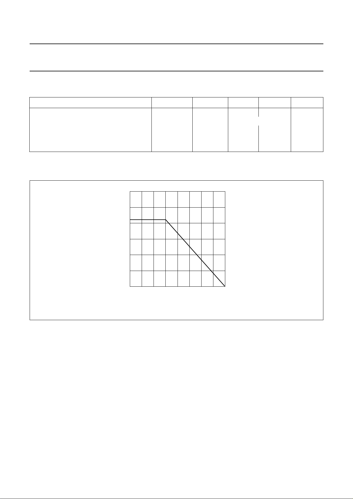
Total power dissipation P
Storage temperature range T
Operating ambient temperature range T
Electrostatic handling
(1)
P
tot
stg
amb
V
es
Note
1. Equivalent to discharging a 200 pF capacitor through a 1.5 kΩ series resistor.
− 18 V
see Fig.4
−65 +150 °C
−40 +85 °C
−2000 +2000 V
P
(W)
3
tot
2
1
0
–50
handbook, halfpage
0 50 150
100
T
amb
Fig.4 Power derating curve.
MLA286
o
C)
(
March 1991 7
Page 8

Philips Semiconductors Product specification
AM/FM radio receiver circuit TEA5594
DC CHARACTERISTICS
All voltages are referenced to pin 10, pin 19 and pin 32; all input currents are positive; all parameters are measured in
application circuit (see Fig.5) at nominal supply voltage V
PARAMETER CONDITIONS SYMBOL MIN. TYP. MAX. UNIT
Supply voltage V
Voltages (FM)
Pin 4 V
Pin 5 V
Pin 7 V
Pin 8 V
Pin 12 V
Pin 27 V
Pin 29 V
Pin 30 V
Pin 31 V
Voltages (AM)
Pin 12 V
Pin 14 V
Pin 15 V
Pins 22 and 23 V
Pin 24 V
Total current consumption
AM part I
FM part I
= 8.5 V; T
P
P
4
5
7
8
12
27
29
30
31
12
14
15
, V
22
23
24
P
P
= 25 °C unless otherwise specified.
amb
2.7 8.5 15 V
− 2.3 − V
− 2.2 − V
− 2.3 − V
− 2.3 − V
− 1.15 − V
− 1.6 − V
− 1.0 − V
− 0.9 − V
− 1.6 − V
− 0.2 − V
− 0.8 − V
− 1.54 − V
− 1.1 − V
− 1.6 − V
− 13
− 24
(1)
(1)
mA
mA
Note
1. Value to be fixed.
March 1991 8
Page 9

Philips Semiconductors Product specification
AM/FM radio receiver circuit TEA5594
AC CHARACTERISTICS
All parameters are measured in test circuit (see Fig.6) at nominal supply voltage V
otherwise specified.
PARAMETER CONDITIONS SYMBOL MIN. TYP. MAX. UNIT
AM SECTION
AM front end
Conversion transconductance V
note 1
= 10 mV
i
V
(pin 15)
AGC
= V
- 0.1 V S
24
V
= V24- 0.45 V S
AGC
C
C
(9)
(9)
IF suppression note 2 α 20 30 − dB
Oscillator (pin 25)
Voltage f = 1.5 MHz V
osc
− 160
Oscillator buffer
Output voltage
(peak-to-peak value) V
IF and detector part
note 3
18
(9)
IF sensitivity;
AF output voltage no AGC;
V
= 90 µVV
i(IF)
o
30 40 60 mV
Signal + noise to noise no AGC;
ratio for an IF input V
AF output voltage V
Total harmonic distortion V
= 90 µVS+N/N 22 24 30 dB
i(IF)
= 1 mV V
i(IF)
= 10 mV;
i(IF)
o
35 50 70 mV
m = 80% THD 0.75 2 5 %
(9)
V
i(IF)
(9)
=
to
mV;
m = 30% THD −
= 6 V; T
P
13.5
1.2
= 25 °C unless
amb
(9)
(9)
(9)
140 − mV
(9)
− %
mA/V
mA/V
mV
Indicator/level detector
Output voltage V
= 0 V V
i(IF)
V
= 200 µVV
i(IF)
V
= 10 mV V
i(IF)
AM IF counter output buffer
Counter “enable”
Output voltage
(peak-to-peak value) V
Counter “disable”
Suppression of 468 kHz V
Overall performance
Total harmonic distortion V
Signal handling THD =
note 4
= 50 mV THD −−8%
i(RF)
(9)
%; m = 0.8% −
March 1991 9
13
13
13
20
20
(9)
(9)
(9)
100 125 − mV
−40 −−dB
560
3200
6600
(9)
(9)
(9)
(9)
−
mV
mV
mV
Page 10

Philips Semiconductors Product specification
AM/FM radio receiver circuit TEA5594
PARAMETER CONDITIONS SYMBOL MIN. TYP. MAX. UNIT
Counter enable circuit
IF counter output OFF V
IF counter output ON V
21
21
FM SECTION
FM front end
Conversion transconductance V
note 5
= 1 mV;
i(RF)
V
= 1.1 V S
AGC
V
= 1 mV;
i(RF)
V
= 0.8 V S
AGC
c
c
Oscillator (pin 26)
Voltage V
osc
Oscillator buffer
Output voltage
(peak-to-peak value) V
IF and demodulator part
note 6
17
IF sensitivity note 7
AF output voltage V
= 40 µV
i(IF)
no mute V
with mute V
o
o
AM suppression note 8 α−
Signal + noise-to-noise no mute;
ratio for an IF input V
AF output voltage V
Total harmonic distortion V
= 40 µVS+N/N 28 46 50 dB
i(IF)
V
= 1 mV S+N/N −
i(IF)
= 1 mV V
i(IF)
i(IF)
= 50 mV
o
∆f = 75 kHz THD − 1 − %
∆f = 22.5 kHz THD −
−−0.8 V
2 − V
P
V
16 24 32 mA/V
5 10 15 mA/V
− 250 - mV
(9)
270 − mV
−3 −10 dB
−20 −30 −40 dB
(9)
(9)
(9)
85
(9)
-dB
− dB
(9)
mV
− %
Indicator/level detector
Output voltage V
= 0 V V
i(IF)
V
= 50 µVV
i(IF)
V
= 1 mV V
i(IF)
AM/FM IF counter output
buffer
Counter “enable” note 5
Output voltage
(peak-to-peak value) V
Counter “disable”
Suppression of 10.7 MHz V
March 1991 10
13
13
13
20
20
(9)
(9)
(9)
− 130 − mV
−40 - − dB
2600
5750
6250
(9)
(9)
(9)
mV
mV
mV
Page 11

Philips Semiconductors Product specification
AM/FM radio receiver circuit TEA5594
PARAMETER CONDITIONS SYMBOL MIN. TYP. MAX. UNIT
Counter enable circuit
IF counter output OFF V
IF counter output ON V
21
21
−−0.8 V
2 − V
AM/FM switch
FM OFF/AM ON V
FM ON/AM OFF V
8-10
24-10
− 00V
− 00V
Notes to the characteristics
1. Input frequency = 1 MHz, output frequency = 468 kHz;
V
C
=
---------------- V
oIF()
iRF()
S
N2 N3⁄
------------------- R
( see TR2 Component data)×
Where R = 1.2 kΩ (total impedance at pin 16).
2. α = 20 log (Vi at fi = 468 kHz)/(Vi at fi = 1 MHz); Vo = 10 mV; no AGC.
3. Input frequency = 468 kHz; m = 30% modulated with f
= 1 kHz; R
mod
= 800 Ω unless
source
otherwise specified.
4. Front-end connected to IF plus detector part (see Fig.5). Input frequency = 1 MHz; m = 80%
modulated with f
= 1 kHz.
mod
5. Input frequency = 100 MHz, output frequency = 10.7 MHz;
V
S
---------------- -
c
V
N1 N2⁄
oIF()
× see TR3 Component data()=
------------------- -
iRF()
R
Where R = 6.6 kΩ (total impedance at pin 2).
6. Input frequency = 10.7 MHz; frequency deviation, ∆f = 22.5 kHz and f
=1 kHz; unless
mod
otherwise specified.
7. Reference: AF output voltage = 0 dB at V
= 1 mV;
i(IF)
No mute: V1 = V8;
With mute: V1 = 0 V.
8. AM suppression is measured with AM only: m = 0.8% and f
FM only: ∆f = 75 kHz and f
= 1 kHz.
mod
= 1 kHz referred to AF output at
mod
9. Value to be fixed.
v
P
V
March 1991 11
Page 12
This text is here in white to force landscape pages to be rotated correctly when browsing through the pdf in the Acrobat reader.This text is here in
_white to force landscape pages to be rotated correctly when browsing through the pdf in the Acrobat reader.This text is here inThis text is here in
white to force landscape pages to be rotated correctly when browsing through the pdf in the Acrobat reader. white to force landscape pages to be ...
March 1991 12
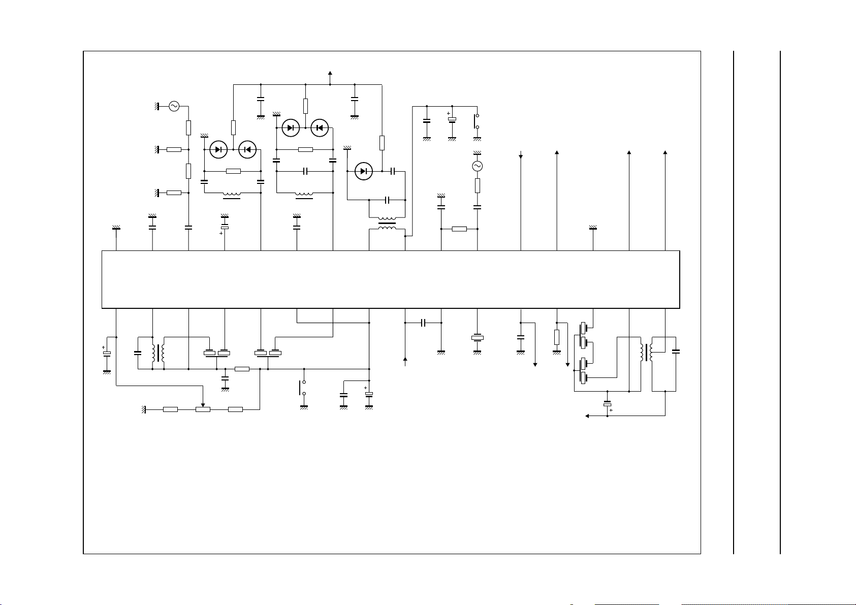
APPLICATION AND TEST INFORMATION
Philips Semiconductors Product specification
AM/FM radio receiver circuit TEA5594
4.7
µF
FM
50 Ω
560 Ω
27 Ω
91 Ω
1 nF
1
2 3 4 5 6 7 8 9 10 11 12 13 14 15 16
TR1
68
pF
N1 N2
688 pF
22 nF
22 nF
47 kΩ
BB204B
100 kΩ
1 nF 1 nF
L1
1 µF
29303132
SFE
10.7MS3
56 Ω
3.3 kΩ2 kΩ8.2 kΩ
28
K2K2
47 kΩ
BB204G
100 kΩ
1 nF 1 nF
3.3 pF
L2
22 nF
27
SFE
10.7MS3
AM
10 nF
33
22
nF
100 kΩ
BB112
TR2
26
390
pF
5.6 pF
N1
N2
TEA5594
47 µF22 nF
22 nF
22 nF
50 Ω
µF
K3
AM
AM
50 Ω
10 nF
CDA
10.7MC1
mono 22 nF
stereo 680 pF
22
kΩ
to pin 24
K1
SFZ468HL3
33 µF
171819202122232425
TR3
N1
N3
180
pF
N2
MLA287
For coil information see Component data.
handbook, full pagewidth
Fig.5 Application circuit for evaluation.
Page 13
This text is here in white to force landscape pages to be rotated correctly when browsing through the pdf in the Acrobat reader.This text is here in
_white to force landscape pages to be rotated correctly when browsing through the pdf in the Acrobat reader.This text is here inThis text is here in
white to force landscape pages to be rotated correctly when browsing through the pdf in the Acrobat reader. white to force landscape pages to be ...
March 1991 13
Philips Semiconductors Product specification
AM/FM radio receiver circuit TEA5594
4.7
µF
1
100
10 nF
100 Ω
22 nF
50 Ω
4.7
pF
L1
4.7
kΩ
28
75 Ω
62 Ω
0.68
4.7 nF100 nF
2 3 4 5 6 7 8 9 10 11 12 13 14 15 16
TR1
N2 N1
300 Ω
µF
68
pF
100
nF
29303132
8-18
pF
274 Ω
AM
kΩ
BB4058
L2
27
K2
SFE
10.7MS3
47 µF100
12
pF
15
8-18
pF
pF
N2 N1
26
TEA5594
nF
1
MΩ
TR2
AM
BB204
10
pF
100 nF
47 µF
100nF47
100 nF
50 Ω
CDA
10.7MC6
µF
100 nF
7.6
5 pF
kΩ
10 nF 10 nF 10 nF
100 nF
15
K3
nF
22
kΩ
787 Ω
50 Ω
8 pF
100
kΩ
180
pF
680 nF
N1
N2
3 kΩ
TR3
1.6
kΩ
7 pF
171819202122232425
N3
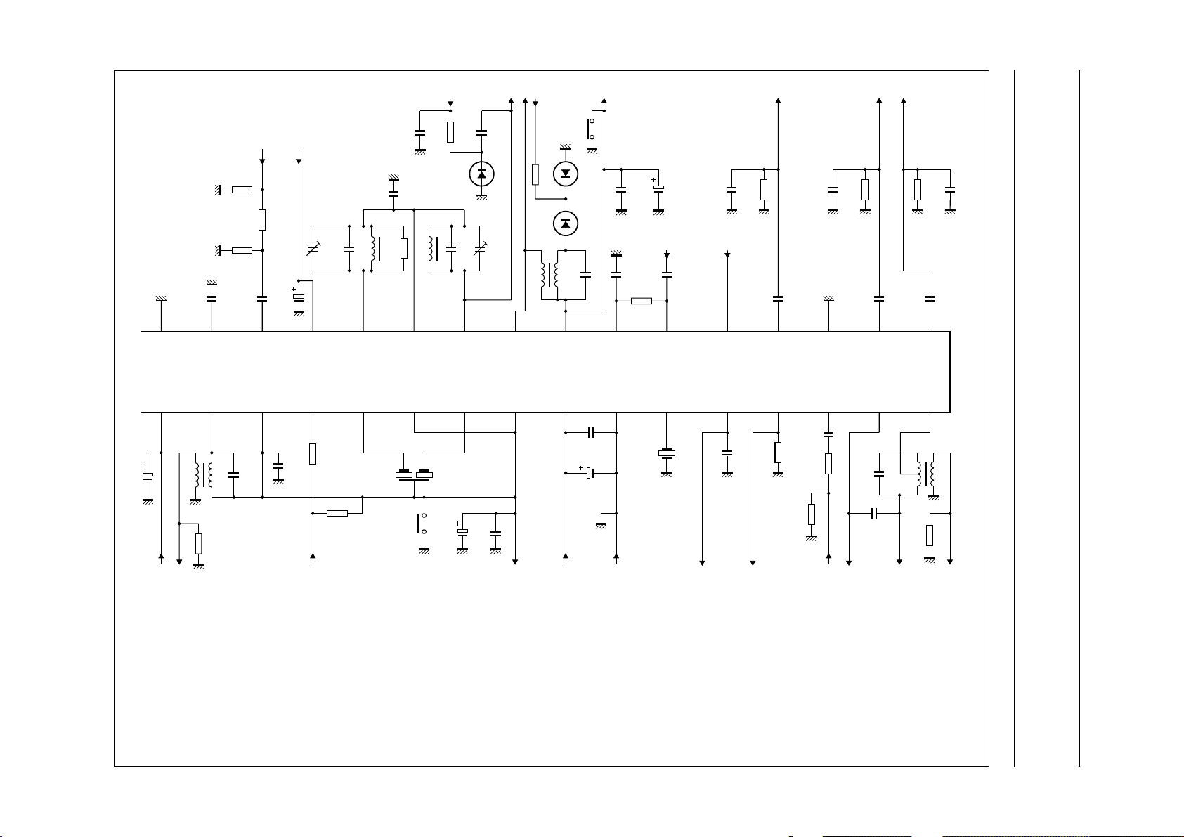
For coil information see Component data.
handbook, full pagewidth
Fig.6 Factory test circuit.
to pin24
MLA288
Page 14
Philips Semiconductors Product specification
AM/FM radio receiver circuit TEA5594
Component data
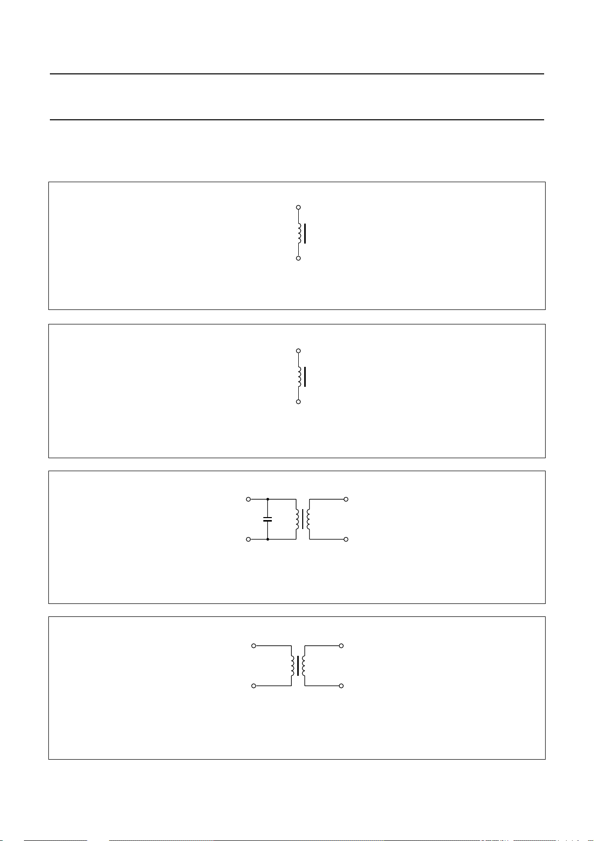
COILS
N1 = 4.5
L = 100 µH
N1 = 4.5
L = 94 µH
handbook, halfpage
1
N1
MLA289
2
Fig.7 FM-RF coil (L1). TOKO equivalent no. MC115.
handbook, halfpage
1
N1
MLA289
2
Fig.8 FM oscillator coil (L2). TOKO equivalent no. A294SNS-1004NK.
handbook, halfpage
N1 = 12
N2 = 2
C= 68 pF (internal)
fo = 10.7 MHz
Wire = 0.07 mm diameter
Coil type TOKO 119BCS-A6515BQG
3
N1 N2
C
1
Fig.9 FM-IF coil (TR1).
handbook, halfpage
N1 = 55
N2 = 55
Lprim = 106 µH
Wire = 0.05 mm diameter
Coil type TOKO 7MCS
3
N1 N2
1
Fig.10 AM oscillator coil (TR2).
March 1991 14
4
6
MLA290
4
6
MLA291
Page 15

Philips Semiconductors Product specification
AM/FM radio receiver circuit TEA5594
handbook, halfpage
N1 = 139
N2 = 15
N3 = 9
C = 180 pF (internal)
Lprim = 660 µH
fo= 468 MHz
Wire = 0.07 mm diameter
Coil type TOKO 7MC
CERAMIC FILTERS
AM-IF (K1). SFZ468HL3.
FM-IF (K2). SFE10.7MS3.
FM detector (K3). CDA10.7MC1 (MC6).
3
C
N1
2
1
N2
N3
MLA292
Fig.11 AM-IF coil (TR3).
4
6
March 1991 15
Page 16
Philips Semiconductors Product specification
AM/FM radio receiver circuit TEA5594
PACKAGE OUTLINE
SDIP32: plastic shrink dual in-line package; 32 leads (400 mil)
D
seating plane
L
Z
32
pin 1 index
e
b
SOT232-1
M
E
A
2
A
A
1
w M
b
1
17
E
c
(e )
M
1
H
1
0 5 10 mm
scale
DIMENSIONS (mm are the original dimensions)
A
A
A
UNIT b
Note
1. Plastic or metal protrusions of 0.25 mm maximum per side are not included.
mm
OUTLINE
VERSION
SOT232-1
max.
4.7 0.51 3.8
12
min.
max.
IEC JEDEC EIAJ
1.3
0.8
b
1
0.53
0.40
REFERENCES
0.32
0.23
cEe M
(1) (1)
D
29.4
28.5
March 1991 16
9.1
8.7
16
(1)
Z
L
3.2
2.8
EUROPEAN
PROJECTION
M
10.7
10.2
E
12.2
10.5
e
1
w
H
0.181.778 10.16
ISSUE DATE
92-11-17
95-02-04
max.
1.6
Page 17

Philips Semiconductors Product specification
AM/FM radio receiver circuit TEA5594
SOLDERING
Introduction
There is no soldering method that is ideal for all IC
packages. Wave soldering is often preferred when
through-hole and surface mounted components are mixed
on one printed-circuit board. However, wave soldering is
not always suitable for surface mounted ICs, or for
printed-circuits with high population densities. In these
situations reflow soldering is often used.
This text gives a very brief insight to a complex technology.
A more in-depth account of soldering ICs can be found in
our
“IC Package Databook”
Soldering by dipping or by wave
The maximum permissible temperature of the solder is
260 °C; solder at this temperature must not be in contact
with the joint for more than 5 seconds. The total contact
time of successive solder waves must not exceed
5 seconds.
DEFINITIONS
Data sheet status
Objective specification This data sheet contains target or goal specifications for product development.
Preliminary specification This data sheet contains preliminary data; supplementary data may be published later.
Product specification This data sheet contains final product specifications.
(order code 9398 652 90011).
The device may be mounted up to the seating plane, but
the temperature of the plastic body must not exceed the
specified maximum storage temperature (T
printed-circuit board has been pre-heated, forced cooling
may be necessary immediately after soldering to keep the
temperature within the permissible limit.
Repairing soldered joints
Apply a low voltage soldering iron (less than 24 V) to the
lead(s) of the package, below the seating plane or not
more than 2 mm above it. If the temperature of the
soldering iron bit is less than 300 °C it may remain in
contact for up to 10 seconds. If the bit temperature is
between 300 and 400 °C, contact may be up to 5 seconds.
stg max
). If the
Limiting values
Limiting values given are in accordance with the Absolute Maximum Rating System (IEC 134). Stress above one or
more of the limiting values may cause permanent damage to the device. These are stress ratings only and operation
of the device at these or at any other conditions above those given in the Characteristics sections of the specification
is not implied. Exposure to limiting values for extended periods may affect device reliability.
Application information
Where application information is given, it is advisory and does not form part of the specification.
LIFE SUPPORT APPLICATIONS
These products are not designed for use in life support appliances, devices, or systems where malfunction of these
products can reasonably be expected to result in personal injury. Philips customers using or selling these products for
use in such applications do so at their own risk and agree to fully indemnify Philips for any damages resulting from such
improper use or sale.
March 1991 17
 Loading...