

Page 1

INTEGRATED CIRCUITS
DATA SH EET
TEA6850
IF filter / amplifier / demodulator for
FM radio receivers
Preliminary specification
File under Integrated Circuits, IC01
July 1994
Page 2

Philips Semiconductors Preliminary specification
IF filter / amplifier / demodulator for FM
TEA6850
radio receivers
FEATURES
• Improved dynamic selectivity and sensitivity because of
tunable IF filter
• Fully integrated, frequency matched FM demodulator
• High linearity
• Unweighted level detector output
• Soft mute
• MPX output for RDS and diversity
• Internal source selector.
QUICK REFERENCE DATA
SYMBOL PARAMETER MIN. TYP. MAX. UNIT
V
P
I
P
supply voltage (pin 7) 7 8.5 10 V
supply current (pin 7) 14 17.5 21 mA
DS200 dynamic selectivity for 200 kHz 22 27 − dB
distance (EMF = 700 µV;
filter bandwidth = 50 kHz)
S/N signal-to-noise ratio 61 67 − dB
(∆f = ±22.5 kHz; f
= 1 kHz)
m
THD total harmonic distortion − 0.3 0.5 %
(∆f = ±75 kHz; f
V
O
AF output signal at pin 4 180 200 220 mV
= 1 kHz)
m
(RMS value)
T
amb
operating ambient temperature −40 −+85 °C
GENERAL DESCRIPTION
The TEA6850 is a monolithic bipolar integrated circuit for
IF filtering, FM demodulation and level detection. Using IF
filters tuned by the demodulated signal, dynamic
selectivity and sensitivity are improved.
ORDERING INFORMATION
EXTENDED TYPE
NUMBER
PINS PIN POSITION MATERIAL CODE
PACKAGE
TEA6850H 44 QFP plastic SOT307
Note
1. SOT307-2; 1996 August 26.
July 1994 2
(1)
Page 3
This text is here in white to force landscape pages to be rotated correctly when browsing through the pdf in the Acrobat reader.This text is here in
_white to force landscape pages to be rotated correctly when browsing through the pdf in the Acrobat reader.This text is here inThis text is here in
white to force landscape pages to be rotated correctly when browsing through the pdf in the Acrobat reader. white to force landscape pages to be ...
July 1994 3
Philips Semiconductors Preliminary specification
IF filter / amplifier / demodulator for FM
radio receivers
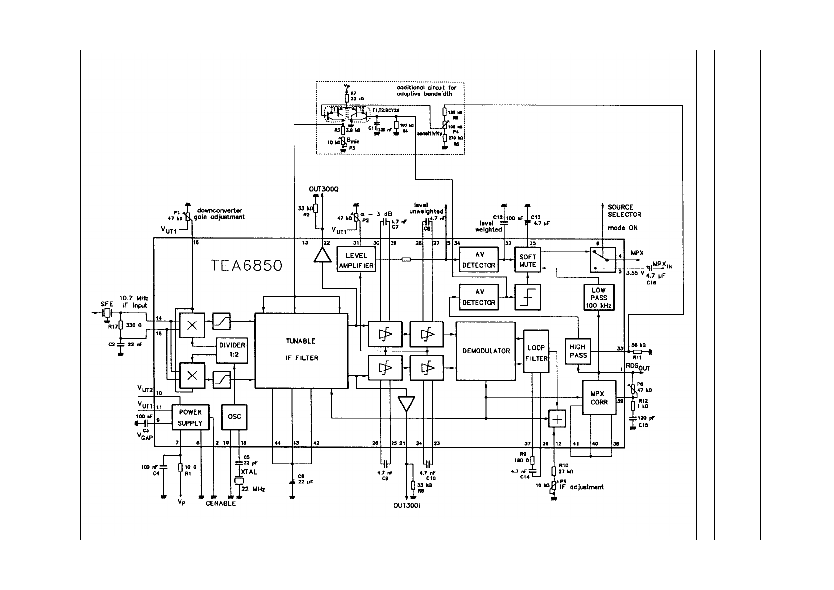
Fig.1 Diagram for adaptive application.
TEA6850
Page 4
Philips Semiconductors Preliminary specification
IF filter / amplifier / demodulator for FM
radio receivers
TEA6850
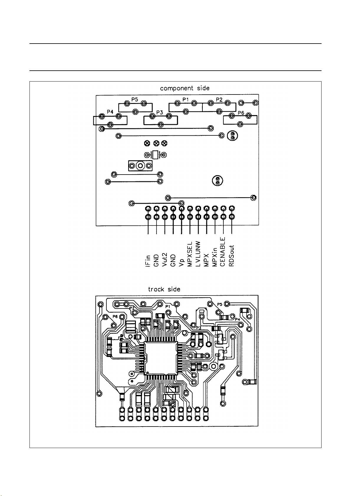
Fig.2 TEA6850H (adaptive version), printed- circuit board.
July 1994 4
Page 5

Philips Semiconductors Preliminary specification
IF filter / amplifier / demodulator for FM
radio receivers
PINNING
SYMBOL PIN DESCRIPTION
RDS
OUT
CENABLE 2 chip enable
MPX
IN
MPX 4 audio frequency output (MPX signal)
LVLUNW 5 unweighted level output
MPXSEL 6 source selector for MPX signal
V
P
GND 8 ground (0 V)
V
GAP
V
UT2
V
UT1
IFADJ 12 input for IF filter frequency adjustment
BWADJ 13 input for IF filter bandwidth adjustment
IF
IN
IF
INI
GAINADJ 16 input for mixer gain adjustment
n.c. 17 not connected
CRYSTAL 18 crystal oscillator input
GND 19 oscillator ground
n.c. 20 not connected
OUT300I 21 IF filter output (0°)
OUT300Q 22 IF filter output (90°)
CLIM1I 23 IF limiter feedback 1
CLIM2I 24 IF limiter feedback 2
CLIM3I 25 IF limiter feedback 3
CLIM4I 26 IF limiter feedback 4
CLIM1Q 27 IF limiter feedback 5
CLIM2Q 28 IF limiter feedback 6
CLIM3Q 29 IF limiter feedback 7
CLIM4Q 30 IF limiter feedback 8
LVLADJ 31 input for level adjustment
LVLWEI 32 weighted level output
IHP60 33 input for high-pass −3 dB adjustment
CHPMUTE 34 output of rectified high-pass signal
CMUTE 35 mute input
DEMOLOOP1 36 demodulator output 1
DEMOLOOP2 37 demodulator output 2
COP2 38 MPX correction output 2
CON2 39 MPX correction input 2
COO1 40 MPX correction output 1
1 output for RDS
3 external audio frequency input (MPX signal)
7 supply voltage (8.5 V)
9 internal reference voltage
10 reference voltage output
11 reference voltage output
14 IF signal input 1
15 IF signal input 2
TEA6850
July 1994 5
Page 6
Philips Semiconductors Preliminary specification
IF filter / amplifier / demodulator for FM
radio receivers
SYMBOL PIN DESCRIPTION
CON1 41 MPX correction input 1
IFLOOP1 42 IF loop filter output 1
IFLOOP2 43 IF loop filter output 2
IFLOOP3 44 IF loop filter output 3
TEA6850
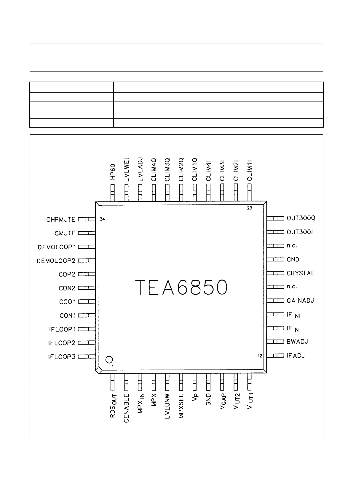
Fig.3 Pin configuration.
July 1994 6
Page 7
Philips Semiconductors Preliminary specification
IF filter / amplifier / demodulator for FM
TEA6850
radio receivers
FUNCTIONAL DESCRIPTION
The first mixer stage at the input of the circuit is for mixing
the 10.7 MHz IF signal to 300 kHz. The IF filter has a
resonance frequency of 300 kHz (adjustable), tunable
from 50 kHz to 500 kHz, and a bandwidth of about 20 kHz
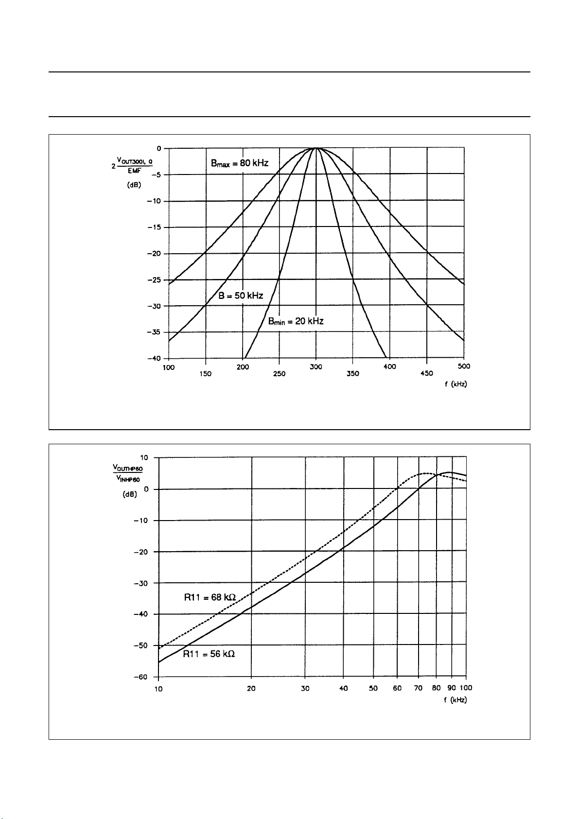
to 80 kHz tunable. Static filter response see Fig.5. The
limiter has a gain of approximately 90 dB, which is virtually
independent from temperature change. The demodulator
is frequency matched with the IF filter.
LIMITING VALUES
In accordance with the Absolute Maximum Rating System (IEC 134).
SYMBOL PARAMETER MIN. MAX. UNIT
V
I
T
T
P
V
P
P
stg
amb
tot
ESD
supply voltage −0.3 +12 V
supply current − 21 mA
storage temperature −55 +125 °C
operating ambient temperature −40 +85 °C
total power dissipation − 252 mW
electrostatic handling for all pins (note 1) −±300 V
Note to the Limiting Values
1. Charge device model class B: equivalent to discharging a 200 pF capacitor through a 0 Ω series resistor.
THERMAL RESISTANCE
SYMBOL PARAMETER THERMAL RESISTANCE
R
th j-a
from junction to ambient in free air 65 K/W
July 1994 7
Page 8

Philips Semiconductors Preliminary specification
IF filter / amplifier / demodulator for FM
TEA6850
radio receivers
DC CHARACTERISTICS
V
= 8.5 V; T
P
SYMBOL PARAMETER MIN. TYP. MAX. UNIT
V
P
I
P
I
P
V
1
V
2
V
3
V
4
V
5
V
6
V
12
V
13
V
14
V
15
V
16
V
18
V
21
V
22
V
23
V
24
V
25
V
26
V
27
V
28
V
29
V
30
V
31
V
32
V
33
V
34
V
35
V
36
V
37
V
38
V
39
V
40
V
41
V
42
V
43
V
44
= +25 °C; all voltages referenced to ground unless otherwise specified.
amb
supply voltage 7 8.5 10 V
supply current (TEA6850 enable) 14 17.5 21 mA
supply current (TEA6850 disable) 320 400 480 µA
voltage at pin 1 2.1 2.4 2.7 V
voltage at pin 2 tbn tbn tbn V
voltage at pin 3 3.3 3.55 3.8 V
voltage at pin 4 3.3 3.55 3.8 V
voltage at pin 5 tbn tbn tbn V
voltage at pin 6 2.1 2.3 2.5 V
voltage at pin 12 0.98 1.08 1.18 V
voltage at pin 13 tbn tbn tbn V
voltage at pin 14 1.8 2 2.2 V
voltage at pin 15 1.8 2 2.2 V
voltage at pin 16 tbn tbn tbn V
voltage at pin 18 3.0 3.3 3.6 V
voltage at pin 21 3.2 3.5 3.8 V
voltage at pin 22 3.2 3.5 3.8 V
voltage at pin 23 3.9 4.2 4.5 V
voltage at pin 24 3.9 4.2 4.5 V
voltage at pin 25 3.9 4.2 4.5 V
voltage at pin 26 3.9 4.2 4.5 V
voltage at pin 27 3.9 4.2 4.5 V
voltage at pin 28 3.9 4.2 4.5 V
voltage at pin 29 3.9 4.2 4.5 V
voltage at pin 30 3.9 4.2 4.5 V
voltage at pin 31 tbn tbn tbn V
voltage at pin 32 tbn tbn tbn V
voltage at pin 33 4.1 4.4 4.7 V
voltage at pin 34 2.7 2.9 3.3 V
voltage at pin 35 2.1 2.4 2.7 V
voltage at pin 36 4.2 4.4 4.6 V
voltage at pin 37 4.2 4.4 4.6 V
voltage at pin 38 2.1 2.4 2.7 V
voltage at pin 39 2.1 2.4 2.7 V
voltage at pin 40 2.1 2.4 2.7 V
voltage at pin 41 2.1 2.4 2.7 V
voltage at pin 42 1.6 1.75 1.9 V
voltage at pin 43 1.6 1.75 1.9 V
voltage at pin 44 1.6 1.75 1.9 V
July 1994 8
Page 9
Philips Semiconductors Preliminary specification
IF filter / amplifier / demodulator for FM
TEA6850
radio receivers
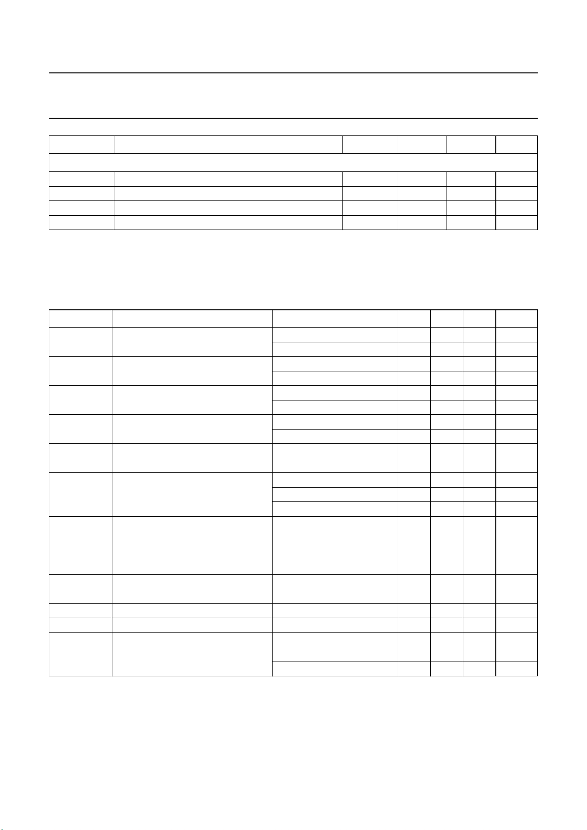
SYMBOL PARAMETER MIN. TYP. MAX. UNIT
Reference voltage source
V
9
V
10
V
11
TK temperature coefficient of V
AC CHARACTERISTICS
= 8.5 V; T
V
P
50 µs de-emphasis; filter bandwidth = 50 kHz overall; −6 dB gain from EMF to IF filter output (pins 21 and 22); in noise
frequency band for S/N measurements 300 Hz to 15 kHz; S/N stereo measurement with ideal decoder; measurements
taken in Fig.4 unless otherwise specified.
SYMBOL PARAMETER CONDITIONS MIN. TYP. MAX. UNIT
DS100 dynamic selectivity for 100 kHz EMF = 700 µV1316−dB
DS200 dynamic selectivity for 200 kHz EMF = 700 µV2227−dB
S/N signal-to-noise ratio mono 61 67 − dB
EMF IF signal S/N = 26 dB; V
EMF input voltage for start of limiting −3 db at MPX output; − 10 20 µV
THD total harmonic distortion ∆f = 75 kHz − 0.3 0.5 %
D
57
EMF admissible maximum input voltage 300 −−mV
A
14-21,22
∆A
DC
V
O
∆V
O
voltage at pin 9 2.4 2.55 2.7 V
voltage at pin 10 2.95 3.25 3.55 V
voltage at pin 11 0.98 1.08 1.2 V
and V
10
= +25 °C; f = 10.7 MHz with fm = 1 kHz, ±22.5 kHz deviaton (∆f = ±22.5 kHz); EMF = 30 mV RMS;
amb
11
− 3.3 − 10−3/K
distance EMF = 14 mV 10 12 − dB
distance EMF = 14 mV 18 22 − dB
stereo 54 57 − dB
= 5 V − 20 45 µV
5
S/N = 46 dB; V
= 5 V − 130 370 µV
5
(RMS value) V5 = 5V
∆f = 100 kHz − 0.5 1 %
f
= 8 kHz; ∆f = 75 kHz − 35%
m
attenuation of third harmonic fm = 19 kHz; ∆f = 6.75 kHz; 14 20 − dB
measured at pin 4 measured at 57 kHz
compared to 57 kHz
∆f = 2 kHz
(RMS value)
gain to IF filter output (adjustable) −−6−dB
downconverter adjustable range −10 −+6dB
MPX output voltage (RMS value) 180 200 220 mV
MPX output voltage ripple 1 kHz < f
23 kHz < f
< 15 kHz −−±2dB
mod
< 53 kHz −−±2dB
mod
July 1994 9
Page 10
Philips Semiconductors Preliminary specification
IF filter / amplifier / demodulator for FM
TEA6850
radio receivers
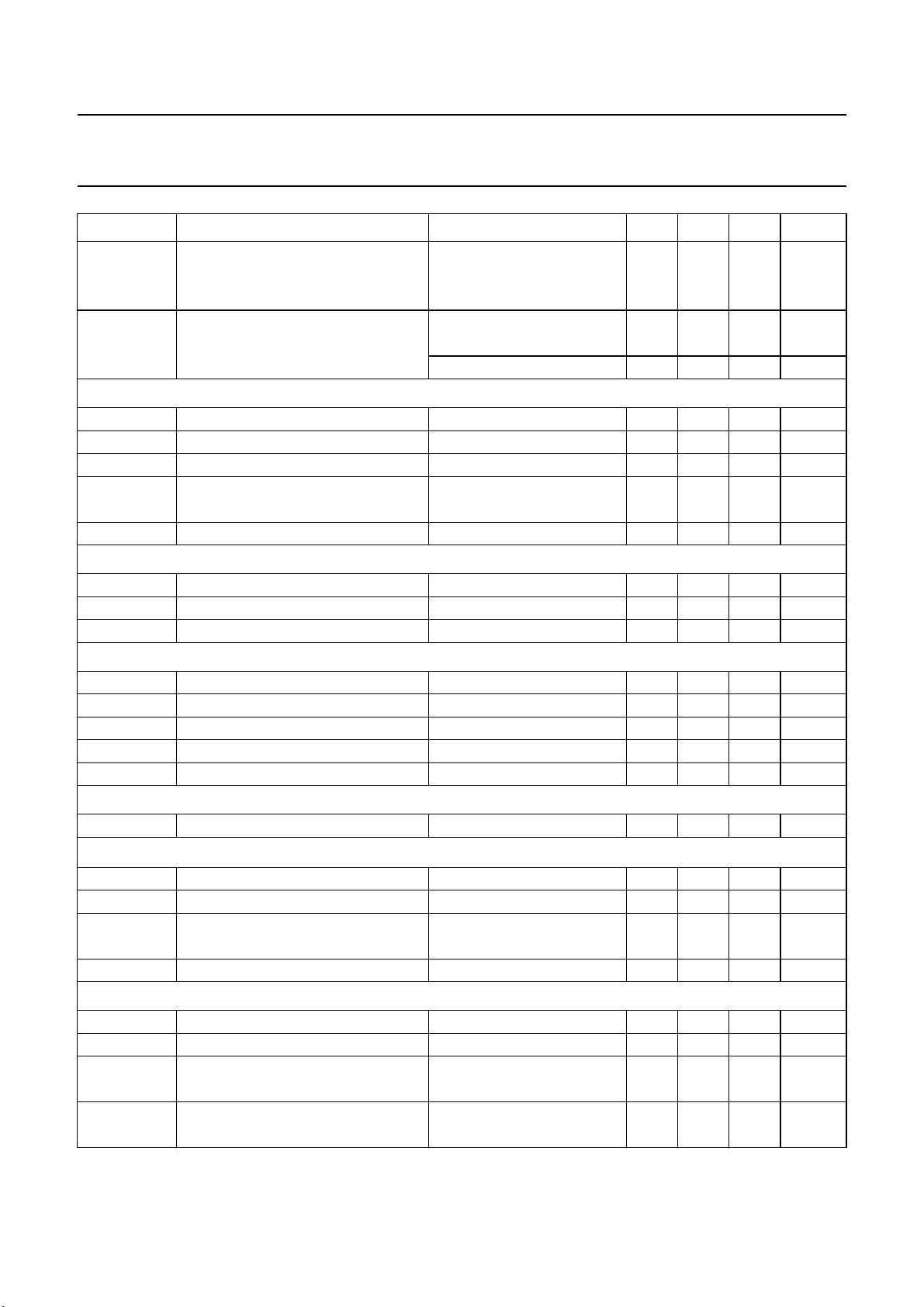
SYMBOL PARAMETER CONDITIONS MIN. TYP. MAX. UNIT
RR power supply ripple rejection f = 200 Hz to 20 kHz; 38 −−dB
V
= 100 mV (on VP);
rmax
ripple at MPX output
α
AM
RDS output (pin 1)
Z
O
R
L
C
L
V
1
t
switch switch on time −−500 ms
10.7 MHz input (pins 14 and 15)
R
i
C
i
V
14
Crystal
f
0
∆f
0/f0
C
0
R
S
∆T
0/T0
Oscillator (measured at pin 18)
V
18
OUT300Q, I output (pins 21 and 22; R
V
21,22
|V
|−|V22| I, Q output level difference −−1.5 mV
21
TC temperature coefficient of − 3.3 − 10
Z
O
Turnable filter (−40 °C<T<+85°C; filter response see Fig.5)
∆F
0
∆B bandwidth temperature shift −50 +3 kHz
B
max
B
min
AM suppression f
= 400 Hz; − 50 − dB
mod
modulation = 30%
500 µV < EMF < 100 mV 40 44 − dB
output impedance −−1kΩ
load resistance 15 −−kΩ
load capacitance −−50 pF
RDS signal output voltage f
= 57 kHz; ∆f = 2 kHz; 4 6 − mV
mod
= ∞; CL = 0
R
L
input resistance 3.5 5 6.5 kΩ
input capacitance −−5pF
residual oscillator signal f
/2 = 11 mHz; RG = 300 Ω− − 30 µV
osc
standard frequency − 22 − MHz
frequency tolerance −100 −+100 ppm
shunt capacitance −−7pF
equivalent series resistance −−120 Ω
temperature drift −40 °C < T < +85 °C −50 − + 50 ppm
22 MHz output level 13 20 40 mV
= 33 KΩ; see Fig.4)
OUT300
output voltage EMF = 75 mV 7 12 14 mV
output voltage
output impedance − 1.26 − kΩ
frequency temperature shift −10 0 +10 kHz
maximum adjustable V13 = 0 V 70 80 − kHz
bandwidth
minimum adjustable − 20 − kHz
bandwidth
−3
/K
July 1994 10
Page 11
Philips Semiconductors Preliminary specification
IF filter / amplifier / demodulator for FM
TEA6850
radio receivers
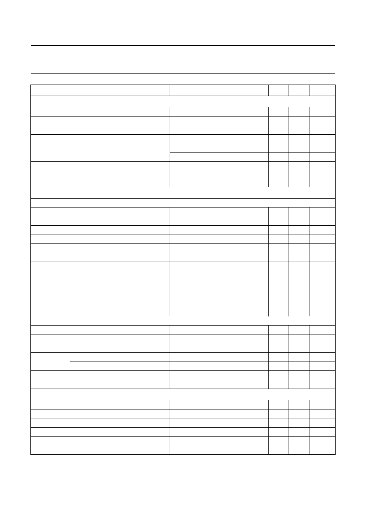
SYMBOL PARAMETER CONDITIONS MIN. TYP. MAX. UNIT
Level amplifier (pin 5; typical curve and adjusting range see Fig.7)
Z
O
TC temperature coefficient of − 3.3 − 10
V
5
S slope of output voltage 100 µV < EMF < 10 mV − 950 − mV/20
V
5
Soft mute (typical curves see Fig.8)
level dependence
EMF start of mute (α = −3 dB) for − 200 −µV
EMF −3 dB adjustment range for IF input 100 − 300 µV
S
M
V
MPX/VMPX0
I
32
τ
mute
τ
unmute
high-pass dependence (see Fig.9)
V
MPX/VMPX0
V
1
I
34
∆V
4
output impedance 8 10 12 kΩ
−3
/K
output voltage
output voltage α = −3 dB for EMF = 200µV; 2.1 2.35 2.6 V
EMF = 100 µV
EMF = 1 mV 2.95 3.3 3.65 V
dB
level shift adjustment range EMF = 0 ±0.5 ±1.0 ±1.5 V
IF input (RMS value)
mute slope at −15 dB 29 32 35 dB/Dec
muting depth EMF < 5 µV; α = −3 dB for −35 −32 −29 dB
EMF = 200 µV
charge current V5 = 4.5 V; V32 = 3.9 V 10 13 17 µA
discharge current V
= 4.5 V; V32 = 5.1 V 20 26 34 µA
5
time constant from unmuted to 0.75 1 1.3 ms
muted
time constant from muted to 1.5 2 2.6 ms
unmuted
muting depth −12 −10 −8dB
voltage at pin 1 (RMS value) f = 60 kHz; 165 185 205 mV
V
MPX/VMPX0
= −3 dB
charge current V34 = 0 V 140 200 260 µA
discharge current V
= 5 V 0.7 1 3 µA
34
residual DC offset at MPX output EMF < 80 µV −−60 mV
80 µV < EMF < 2 mV −−60 mV
MPX output (pin 4)
R
O
R
L
C
L
V
4
V
4
output resistance −−100 Ω
load resistance V4 ≤ 1 V 3 −−kΩ
load capacitance −−50 pF
clipping DC voltage 1.5 − 7V
residual signal of 300 kHz and −−10 mV
higher harmonics (RMS value)
July 1994 11
Page 12
Philips Semiconductors Preliminary specification
IF filter / amplifier / demodulator for FM
TEA6850
radio receivers
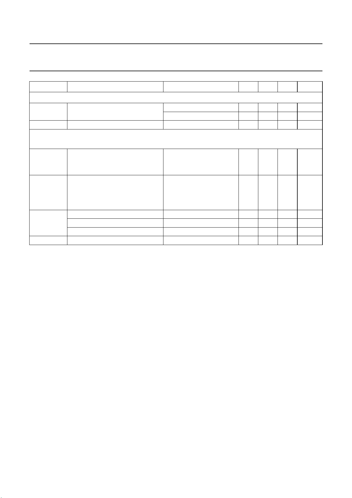
SYMBOL PARAMETER CONDITIONS MIN. TYP. MAX. UNIT
CENABLE (pin 2)
V
2
R
I
Source selector isolation
(f < 12.5 kHz; mode TEA6850 signal: V
V
MPX/VMPXIN
V
MPX/VMPX0
R
I
I
6
voltage range chip enable −0.3 +0.6 +1.1 V
chip disable 1.9 2.4 5.5 V
input resistance 100 −−kΩ
> 1.9 V or pin not connected; mode external signal: V6 < 1.1 V)
6
isolation of external signal mode TEA6850 signal; −70 −80 − dB
∆f = 0; V
MPXIN
= 200 mV;
f = 12.5 kHz
isolation of TEA6850 signal mode external signal; −70 −80 − dB
∆f = 22.5 kHz;
Rg (pin 3) < 10 kΩ;
f
= 12.5 kHz
mod
input resistance at pin 6 V6> 1.9 V 1 −−MΩ
V
< 1.1 V 3 −−kΩ
6
input resistance at pin 3 23 30 37 kΩ
input current V
< 1.1 V −−20 µA
sselect
July 1994 12
Page 13
This text is here in white to force landscape pages to be rotated correctly when browsing through the pdf in the Acrobat reader.This text is here in
_white to force landscape pages to be rotated correctly when browsing through the pdf in the Acrobat reader.This text is here inThis text is here in
white to force landscape pages to be rotated correctly when browsing through the pdf in the Acrobat reader. white to force landscape pages to be ...
July 1994 13
Philips Semiconductors Preliminary specification
IF filter / amplifier / demodulator for FM
radio receivers
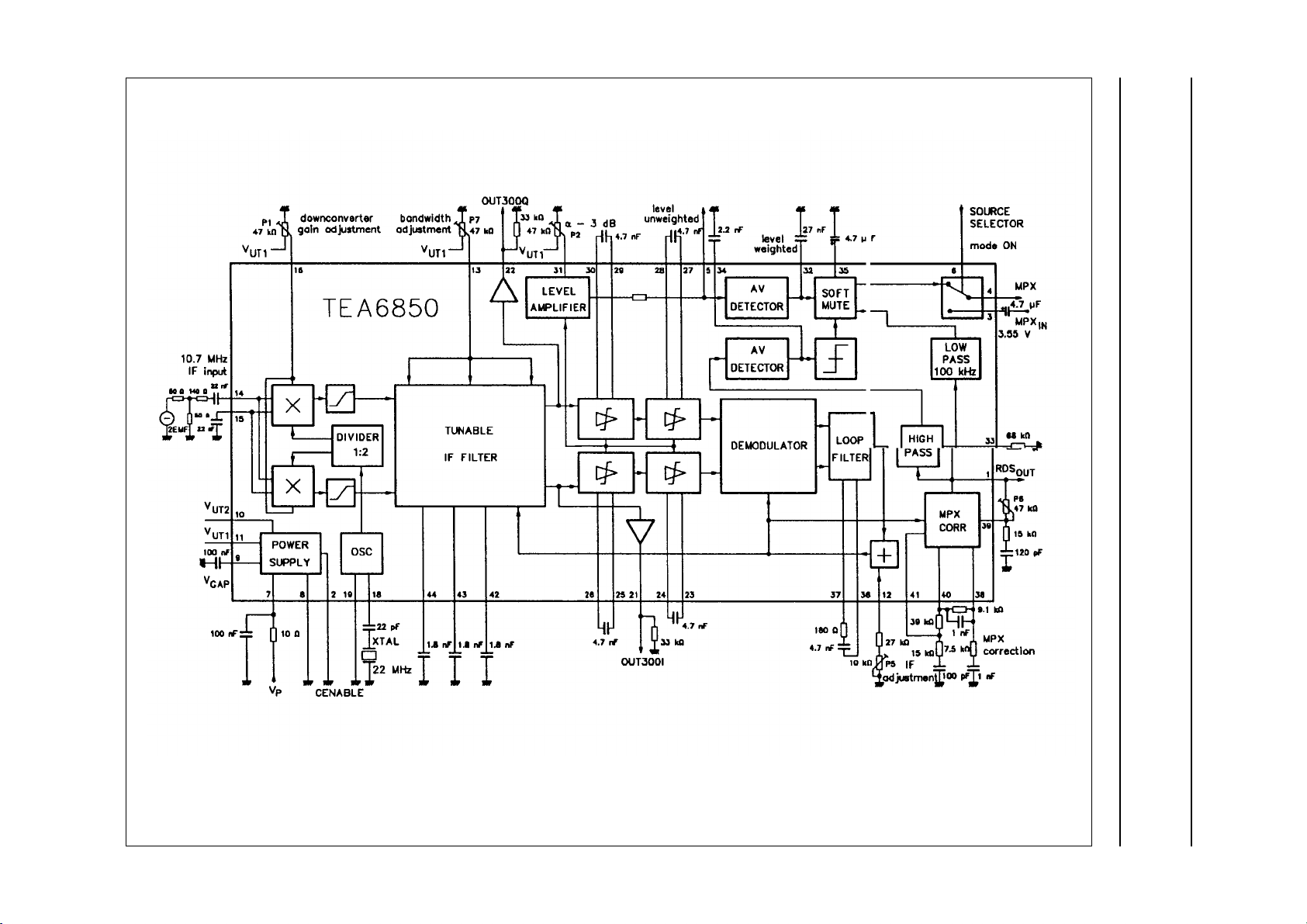
Fig.4 Test circuit.
TEA6850
Page 14
Philips Semiconductors Preliminary specification
IF filter / amplifier / demodulator for FM
radio receivers
TEA6850
Fig.5 IF filter frequency response.
Fig.6 High-pass frequency response (see Fig.1).
July 1994 14
Page 15
Philips Semiconductors Preliminary specification
IF filter / amplifier / demodulator for FM
radio receivers
TEA6850
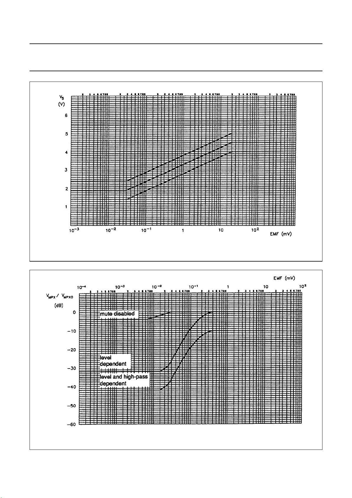
Fig.7 LEVELAMP output voltage.
Fig.8 Soft mute curve.
July 1994 15
Page 16
Philips Semiconductors Preliminary specification
IF filter / amplifier / demodulator for FM
radio receivers
TEA6850
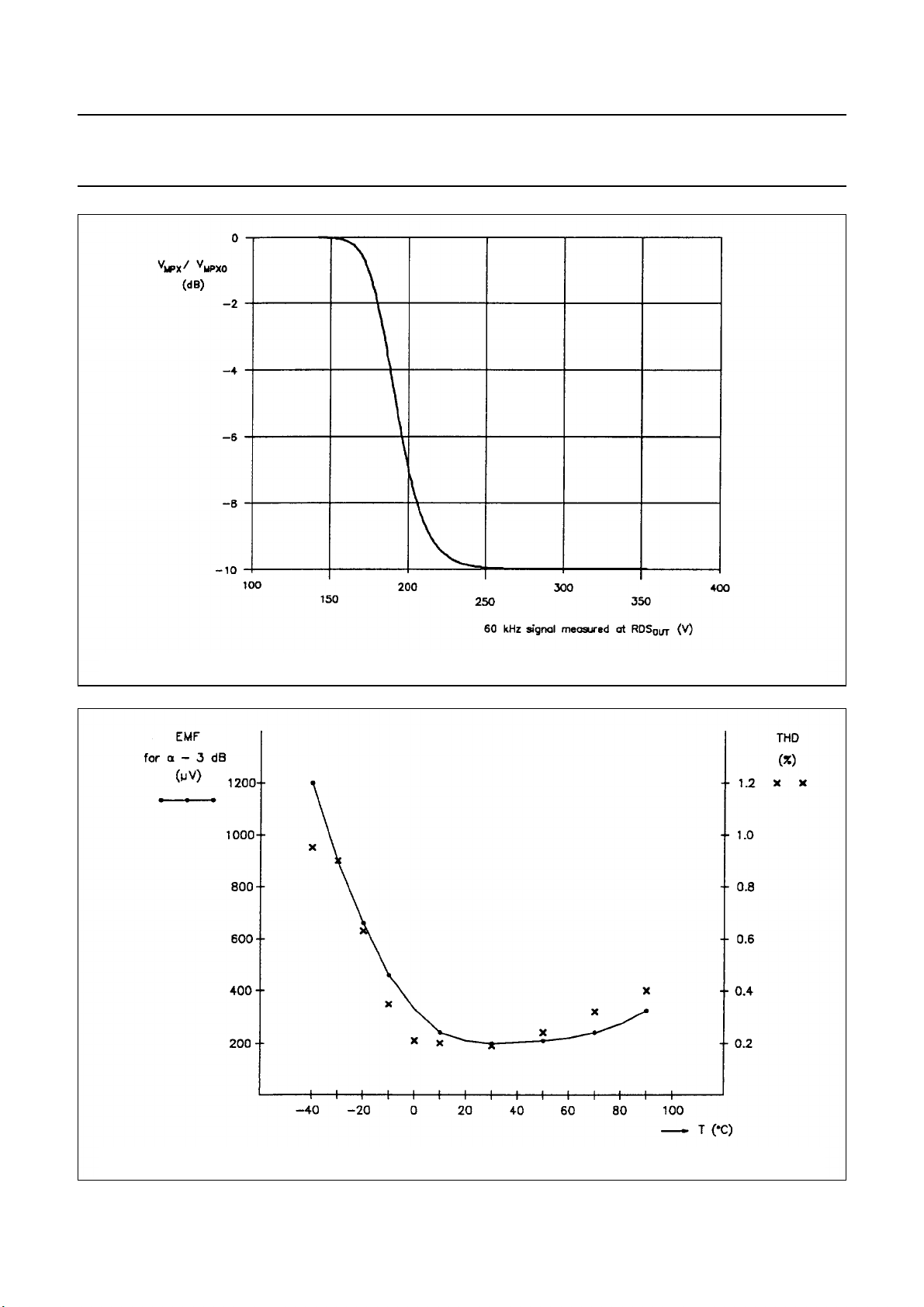
Fig.9 High-pass mute curve.
Fig.10 Temperature dependence of α − 3 dB and THD.
July 1994 16
Page 17

Philips Semiconductors Preliminary specification
IF filter / amplifier / demodulator for FM
radio receivers
APPENDIX
Alignment procedure for the test circuit (see Fig.4)
1. Connect a spectrum analyser to pin 21 or pin 22. Set
centre frequency to 300 kHz and frequency span from
200 kHz to 400 kHz.
2. Set frequency of RF-generator to 10.7 MHz, EMF-level
to 4 mV RMS, modulation frequency to 1 kHz and
frequency deviation to 75 kHz.
3. Turn poti P7 in the mid position. Align centre frequency
of the tunable IF-filter with poti P5. The alignment is
correct, if the spectrum measured at pin 21 is
symmetric.
4. Set frequency deviation of RF-generator to zero (EMF
= 4 mV RMS). Align the downconverter gain with poti
P1. The alignment is correct, if the level at pin 21 is 2
mV RMS.
5. Short pin 36 and pin 37. Set frequency of
RF-generator to 10.6 MHz respectively 10.8 MHz
(EMF = 4 mV RMS, ∆f = 0). Align bandwidth of the
tunable IF-filter with poti P7. The alignment is correct,
if the level measured at 200 kHz respectively 400 kHz
is 21 dB below the maximum. Remove the short.
6. Set frequency of the RF-generator to 10.7 MHz,
EMF-level to 20 mV RMS, modulation frequency to 1
kHz and frequency deviation to 22.5 kHz. Measure
level of the 1 kHz signal at pin 4. Set the EMF-level to
200 µV. Align start of mute (α − 3 dB) with poti P2.
7. Set EMF-level back to 20 mV RMS and vary the
modulation frequency. Align MPX output voltage ripple
(see ∆V
in the AC CHARACTERISTICS) with poti P6.
O
TEA6850
July 1994 17
Page 18
Philips Semiconductors Preliminary specification
IF filter / amplifier / demodulator for FM
radio receivers
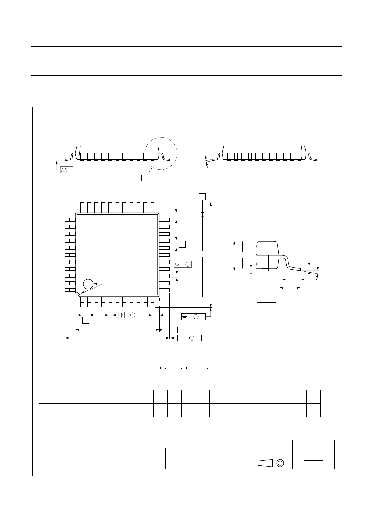
PACKAGE OUTLINE
QFP44: plastic quad flat package; 44 leads (lead length 1.3 mm); body 10 x 10 x 1.75 mm
c
y
X
A
33 23
34
22
Z
E
TEA6850
SOT307-2
e
w M
b
p
pin 1 index
44
1
w M
b
0.25
p
D
H
D
cE
p
0.40
0.25
0.20
0.14
D
10.1
9.9
e
DIMENSIONS (mm are the original dimensions)
mm
A
max.
2.10
0.25
0.05
1.85
1.65
UNIT A1A2A3b
Note
1. Plastic or metal protrusions of 0.25 mm maximum per side are not included.
12
11
Z
D
B
v M
0 2.5 5 mm
scale
(1)
(1) (1)(1)
eH
H
10.1
9.9
12.9
0.8 1.3
12.3
v M
D
H
E
A
B
E
12.9
12.3
E
LL
0.95
0.55
A
p
A
2
A
1
detail X
Z
D
0.15 0.10.15
1.2
0.8
(A )
3
L
p
L
Zywv θ
E
1.2
0.8
θ
o
10
o
0
OUTLINE
VERSION
SOT307-2
IEC JEDEC EIAJ
REFERENCES
July 1994 18
EUROPEAN
PROJECTION
ISSUE DATE
95-02-04
97-08-01
Page 19

Philips Semiconductors Preliminary specification
IF filter / amplifier / demodulator for FM
radio receivers
SOLDERING
Introduction
There is no soldering method that is ideal for all IC
packages. Wave soldering is often preferred when
through-hole and surface mounted components are mixed
on one printed-circuit board. However, wave soldering is
not always suitable for surface mounted ICs, or for
printed-circuits with high population densities. In these
situations reflow soldering is often used.
This text gives a very brief insight to a complex technology.
A more in-depth account of soldering ICs can be found in
our
“IC Package Databook”
Reflow soldering
Reflow soldering techniques are suitable for all QFP
packages.
The choice of heating method may be influenced by larger
plastic QFP packages (44 leads, or more). If infrared or
vapour phase heating is used and the large packages are
not absolutely dry (less than 0.1% moisture content by
weight), vaporization of the small amount of moisture in
them can cause cracking of the plastic body. For more
information, refer to the Drypack chapter in our
Reference Handbook”
Reflow soldering requires solder paste (a suspension of
fine solder particles, flux and binding agent) to be applied
to the printed-circuit board by screen printing, stencilling or
pressure-syringe dispensing before package placement.
Several techniques exist for reflowing; for example,
thermal conduction by heated belt. Dwell times vary
between 50 and 300 seconds depending on heating
method. Typical reflow temperatures range from
215 to 250 °C.
Preheating is necessary to dry the paste and evaporate
the binding agent. Preheating duration: 45 minutes at
45 °C.
(order code 9398 652 90011).
“Quality
(order code 9397 750 00192).
TEA6850
Wave soldering
Wave soldering is not recommended for QFP packages.
This is because of the likelihood of solder bridging due to
closely-spaced leads and the possibility of incomplete
solder penetration in multi-lead devices.
If wave soldering cannot be avoided, the following
conditions must be observed:
• A double-wave (a turbulent wave with high upward
pressure followed by a smooth laminar wave)
soldering technique should be used.
• The footprint must be at an angle of 45° to the board
direction and must incorporate solder thieves
downstream and at the side corners.
Even with these conditions, do not consider wave
soldering the following packages: QFP52 (SOT379-1),
QFP100 (SOT317-1), QFP100 (SOT317-2),
QFP100 (SOT382-1) or QFP160 (SOT322-1).
During placement and before soldering, the package must
be fixed with a droplet of adhesive. The adhesive can be
applied by screen printing, pin transfer or syringe
dispensing. The package can be soldered after the
adhesive is cured.
Maximum permissible solder temperature is 260 °C, and
maximum duration of package immersion in solder is
10 seconds, if cooled to less than 150 °C within
6 seconds. Typical dwell time is 4 seconds at 250 °C.
A mildly-activated flux will eliminate the need for removal
of corrosive residues in most applications.
Repairing soldered joints
Fix the component by first soldering two diagonallyopposite end leads. Use only a low voltage soldering iron
(less than 24 V) applied to the flat part of the lead. Contact
time must be limited to 10 seconds at up to 300 °C. When
using a dedicated tool, all other leads can be soldered in
one operation within 2 to 5 seconds between
270 and 320 °C.
July 1994 19
Page 20

Philips Semiconductors Preliminary specification
IF filter / amplifier / demodulator for FM
TEA6850
radio receivers
DEFINITIONS
Data sheet status
Objective specification This data sheet contains target or goal specifications for product development.
Preliminary specification This data sheet contains preliminary data; supplementary data may be published later.
Product specification This data sheet contains final product specifications.
Limiting values
Limiting values given are in accordance with the Absolute Maximum Rating System (IEC 134). Stress above one or
more of the limiting values may cause permanent damage to the device. These are stress ratings only and operation
of the device at these or at any other conditions above those given in the Characteristics sections of the specification
is not implied. Exposure to limiting values for extended periods may affect device reliability.
Application information
Where application information is given, it is advisory and does not form part of the specification.
LIFE SUPPORT APPLICATIONS
These products are not designed for use in life support appliances, devices, or systems where malfunction of these
products can reasonably be expected to result in personal injury. Philips customers using or selling these products for
use in such applications do so at their own risk and agree to fully indemnify Philips for any damages resulting from such
improper use or sale.
July 1994 20
 Loading...