

BUS-CONTROLLED AUDIO MATRIX SWITCH
GND
CAPACITANCE
L1
L2
L3
L4
L5
LOUT1
ROUT1
LOUT2
ROUT2
SDA
SCL
ADDR
R1
R2
R3
R4
R5
ROUT4
LOUT4
ROUT3
LOUT3
V
S
1
2
3
4
5
6
7
8
9
10
20
19
18
17
16
15
24
23
22
21
11
12
25
13
14
28
27
26
NC
NC
NC
NC
■ 5 Stereo Inputs
■ 4 Stereo Ouputs
■ Gain Control 0/2/4/6dB/Mute for each Output
■ cascadable (2 different addresses)
■ Serial Bus Controlled
■ Very low Noise
■ Very low Distorsion
DESCRIPTION
The TEA6420 switches 5 s tereo audio inputs on
4stereo outputs.
All the switching possibilities are changed through
2
the I
C bus.
TEA6420
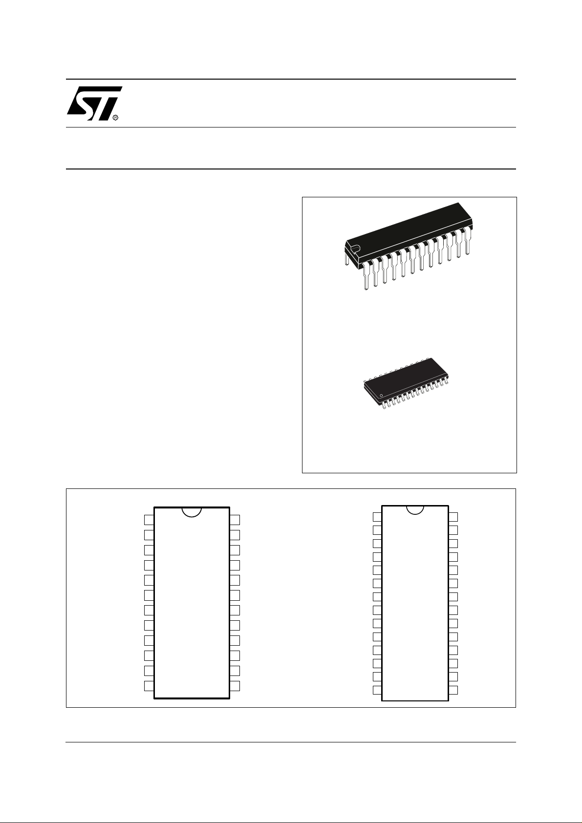
SHRINK DIP 24
(Plastic Package)
ORDER CODE: TEA6420
SO28
(Plastic Micropackage)
ORDER CODE: TEA6420D
Figure 1. PIN CONNECTIONS
S
L1
L2
L3
L4
L5
1
2
3
4
5
6
7
8
9
10
11
12
24
23
22
21
20
19
18
17
16
15
14
13
SDA
SCL
ADDR
R1
R2
R3
R4
R5
ROUT4
LOUT4
ROUT3
LOUT3
GND
CAPACITANCE
V
February 2006 1/7
LOUT1
ROUT1
LOUT2
ROUT2
6420-01.eps - 6420-02.eps
1

TEA6420
Figure 2. BLOCK DIAGRAM
RIGHT INPUTS
V
GND
T
E
GAIN = 0/2/4/6dB
A
6
4
2
RIGHT
OUTPUTS
0
S
C
SUPPLY
BUS DECODER
SDA
SCL
ADDR
LEFT
OUTPUTS
LEFT INPUTS
GAIN = 0/2/4/6dB
6420-03.eps
2/7
1

ABSOLUTE MAXIMUM RATINGS
Symbol Parameter Value Unit
V
T
OPER
T
CC
stg
Supply Voltage (Pin 9) 12 V
Operating Ambient Temperature Range 0 to +70
Storage Temperature Range -20 to +150
THERMA L D ATA
Symbol Parameter+ Value Unit
R
(j-a)
th
Junction-Ambient Thermal Resistance SDIP24
SO28
75
75
o
ELECTRICAL CHARACTERISTICS
TA = 25oC, VS = 10V, RL = 10kΩ, RG = 600Ω, f = 1kHz (unless otherwise specified)
Symbol Parameter Test Conditions Min. Typ. Max. Unit
SUPPLY
V
S
I
S
Supply Voltage
Supply Current
SVR Ripple Rejection V
MATRIX
V
IN
R
I
C
S
Input DC Level
Input Resistance
Channel Separation VIN = 2V
OUTPUT BUFFER
V
R
OUT
OUT
e
NI
Output DC Level
Output Resistance
Input Noise BW = 20 - 20kHz, flat 3 µV
S/N Signal to Noise Ratio V
G
min
G
max
Min. Gain
Max. Gain
d Distortion V
V
CL
R
L
Clipping Level d = 0.3% 2 2.5 V
Output Load Resistance
BUS INPUT
V
IL
V
IN
I
I
V
O
R
pu
Input Low Voltage
Input High Voltage
Input Current
Output Voltage IO = 3mA ; SDA Acknowledge pin 0.4 V
ADDR Pullup Resistor Note 40 50 k
= 500mV
IN
RMS
, BW = 20 - 20kHz 70 80 dB
RMS
Gain = 0dB
f = 1kHz Gain = 6dB
IN
IN
= V
= V
OUT
OUT
= 1V
= 1V
RMS
RMS
8 9 10.2 V
58mA
4.5 5 5.5 V
30 50 100 k
80
70
90
82
4.5 5 5.5 V
70 200 W
110 dB
-1 0 + 1 dB
567dB
0.01 0.05 %
2k
1.5 V
3V
- 10 10 µA
TEA6420
o
C
o
C
C/W
Ω
dB
dB
RMS
Ω
Ω
3/7
1

TEA6420
SOFTWARE SPECIFICATION
1. Chip address
Address HEX ADDR
1001 1000 98 0
1001 1010 9A 1
2. Data bytes
Output select
X0
0
1
1
0
1
0
1
G
1
G
0
I
2
I
1
I
0
Output 1
Output 2
Output 3
Output 4
Input select
XQ
1
Q0 G
1
G
0
0
0
0
0
1
1
0
0
1
1
0
0
0
1
0
1
0
1
Input 1
Input 2
Input 3
Input 4
Input 5
Mute
Gain select
XQ
1
Q0 0
0
0
1
1
1
0
1
I
2
I
1
I
0
Gain = 6 dB
Gain = 4 dB
Gain = 2 dB
Gain = 0 dB
X = don’t care - MSB is transmitted first
Example : X1001100
connects output 3 with input 5 at a gain of 4dB
The following are selected after power-on reset : input 5 selected for all outputs ; gain = 0dB.
4/7
1

TYPICAL APPLICATION
1
2
3
4
5
6
7
8
9
10
11
12 13
14
15
16
17
18
19
20
21
22
23
24
µ
22 F
100nF
C
1
C
2
C
3
C
4
C
5
C
11
C
12
C
13
C
14
CH2
Output
L
R
L
R
CH1
Output
Left
Inputs
C
15
C
16
C
C
17
18
C
10
C
C
9
8
C
C
7
6
SW
R
L
CH3
Output
R
L
CH4
Output
Right
Inputs
Bus
Inputs
SCL
SDA
T
E
A
6
4
2
0
+9V
Figure 3.
TEA6420
6420-08.04
5/7
1

TEA6420
PACKAGE MECHANICAL DATA
24 PINS - PLASTIC DIP
Figure 4. 24-Pin Package
B
E
E1
A2
A1
LA
eB1
D
Stand-off
c
e1
e2
E
24
1
28 PINS - PLAS TIC SO
Figure 5. 28-Pin Package
13
F
12
SDIP24
e3
e2
.015
0,38
Gage Plane
6/7
1

TEA6420
Information furnished is believed to be accurate and reliable. However, STMicroelectronics assumes no responsibility for the consequences
of use of such information nor for any infringement of patents or other rights of third parties which may result from its use. No license is granted
by implic ation or o th erwise un der any pat ent or patent right s of STMi croelectr oni cs. Specifications menti oned in th i s publication are subject
to change without notice. This publication supersedes and replaces all information previously supplied. STMicroelectronics products are not
authorized for use as c ritical components in li fe support devices or syst em s without the expre ss wri t ten approval of STMic roelectronics.
The ST logo is a registered trademark of STMicroelectronics
2006 STMicroelectronics - All Rights Reserved.
Purchase of I
Australi a - Belgium - Brazil - Canada - China - Czech Republic - Finland - Fr ance - Germany - Hong Kong - India - Israel - Italy - Japan -
Malaysia - Malta - Morocco - Singapore - Spain - Sweden - Switzerland - United Kingdom - United States of America .
2
C Components by STMicroelectronics conveys a license under the Philips I2C Patent. Rights to use these components in an
2
I
C system i s granted pro vi ded that th e sy stem conforms to the I2C Standard Specification as defined by Philips.
http://www.s t. com
STMicroelectronics Grou p of Compan i es
7/7
 Loading...