

Page 1
Features
■ Low forwarded voltage drop
■ High reliability
■ High surge current capability
■ Soft switching for reduced EMI disturbances
■ Planar technology
Description
The STTH112, which is using ST ultrafast high
voltage planar technology, is specially suited for
free-wheeling, clamping, snubbering,
demagnetization in power supplies and other
power switching applications
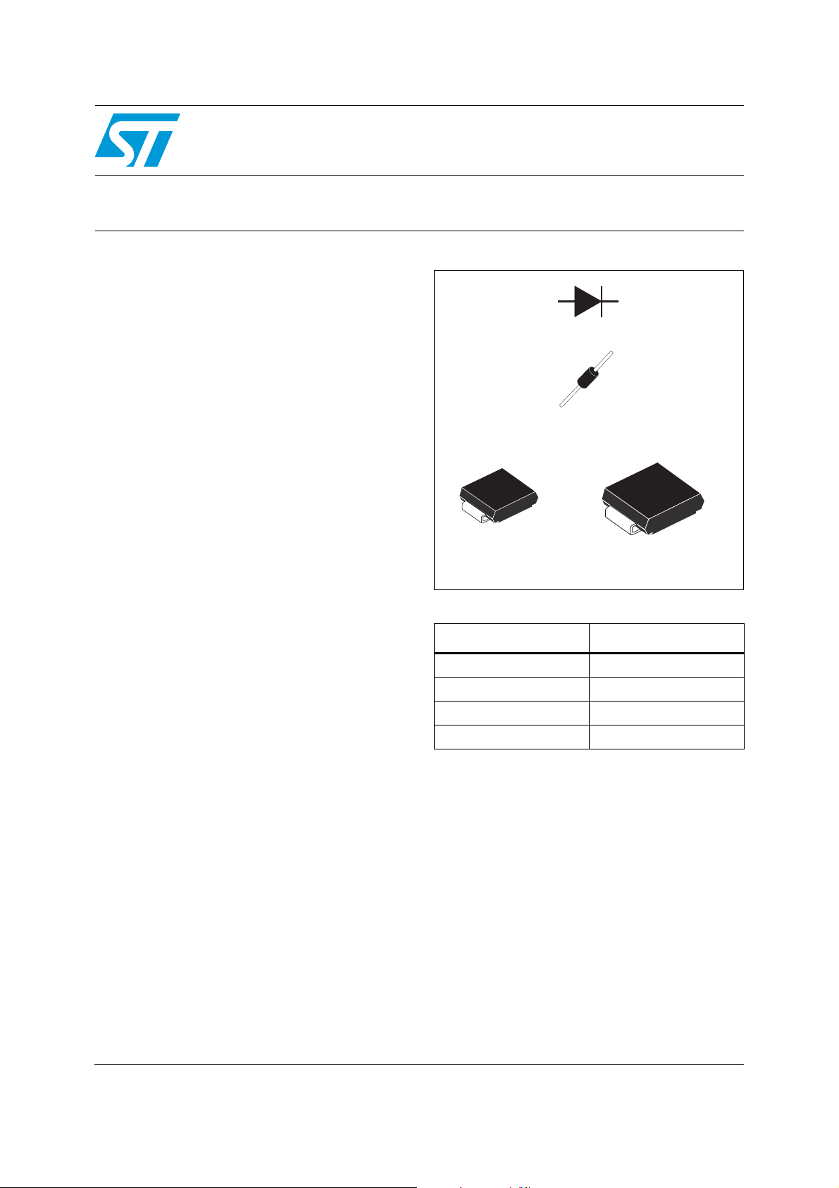
STTH112
High voltage ultrafast rectifier
DO-41
STTH112
SMA
STTH112A
SMB
STTH112U
Table 1. Device summary
Symbol Value
I
F(AV)
V
RRM
T
j (max)
V
F (max)
1 A
1200 V
175 °C
1.65 V
October 2009 Doc ID 9343 Rev 5 1/8
www.st.com
8
Page 2
Electrical characteristics STTH112
1 Electrical characteristics
Absolute ratings (limiting values)
Symbol Parameter Value Unit
V
V
(RMS)
Repetitive peak reverse voltage 1200 V
RRM
Voltage rms 850 V
Tl = 85°C δ =0.5 DO-41
I
F(AV)
Average forward current
1ATl = 115°C δ =0.5 SMA
Tl = 125°C δ =0.5 SMB
DO-41 20
I
Forward surge current t = 8.3 ms
FSM
18
SMB
T
Table 2. Thermal parameters
Storage temperature range - 50 + 175 °C
stg
Maximum operating junction temperature + 175 °C
T
j
Symbol Parameter Value Unit
L = 10 mm DO-41 45
R
th (j-l)
Junction to lead
SMA 30
°C/W
SMB 25
R
th (j-a)
Table 3. Static electrical characteristics
Junction to ambient L = 10 mm DO-41 110
ASMA
Symbol Parameter Tests conditions Min. Typ. Max. Unit
Tj = 25 °C 5
I
Reverse leakage current VR = 1200 V
R
V
Forward voltage drop IF = 1 A
F
Table 4. Dynamic electrical characteristics
= 125 °C 50
T
j
= 25 °C 1.9
T
j
= 125 °C 1.17 1.65
j
= 150 °C 1.10 1.55
T
j
Symbol Parameter Tests conditions Min. Typ. Max. Unit
I
= 0.5 A
t
Reverse recovery time
rr
t
Forward recovery time IF = 1 A
fr
V
Forward recovery voltage 30 V
FP
F
Irr = 0.25 A IR = 1A
/dt = 50 A/µs
dI
F
VFR = 1.1 x V
Fmax
= 25 °C 75 ns
T
j
500 ns
Tj = 25 °C
2/8 Doc ID 9343 Rev 5
µA
VT
Page 3
STTH112 Electrical characteristics
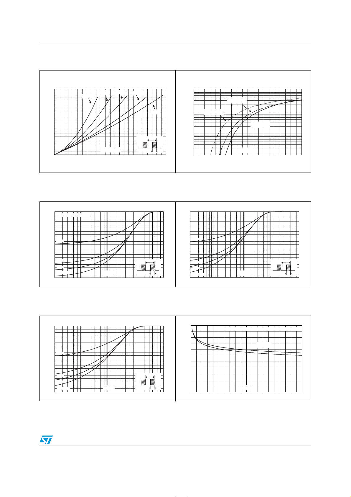
0.00.51.01.52.02.53.03.54.04.55.0
Figure 1. Conduction losses versus average
current
P(W)
2.2
2.0
1.8
1.6
1.4
1.2
1.0
0.8
0.6
0.4
0.2
0.0
0.0 0.1 0.2 0.3 0.4 0.5 0.6 0.7 0.8 0.9 1.0 1.1 1.2
δ = 0.05
δ = 0.1
I (A)
F(AV)
δ = 0.2
δ = 0.5
δ
=tp/T
δ = 1
T
tp
Figure 3. Relative variation of thermal
impedance junction ambient versus
pulse duration (DO-41)
Z/R
th(j-c) th(j-c)
1.0
epoxy FR4, L = 10mm
0.9
0.8
0.7
0.6
δ = 0.5
0.5
0.4
0.3
δ = 0.2
0.2
δ = 0.1
0.1
Single pulse
0.0
1.E-01 1.E+00 1.E+01 1.E+02 1.E+03
leads
T
t (s)
p
δ
=tp/T
tp
Figure 2. Forward voltage drop versus
forward current
I (A)
FM
100.0
T=125°C
j
(maximum values)
T=125°C
10.0
1.0
0.1
j
(typical values)
V (V)
FM
T=25°C
j
(maximum values)
Figure 4. Relative variation of thermal
impedance junction ambient versus
pulse duration (epoxy FR4) (SMA)
Z/R
th(j-c) th(j-c)
1.0
0.9
0.8
0.7
0.6
= 0.5
δ
0.5
0.4
0.3
= 0.2
δ
0.2
= 0.1
δ
0.1
Single pulse
0.0
1.E-01 1.E+00 1.E+01 1.E+02 1.E+03
t (s)
p
δ
T
=tp/T
tp
Figure 5. Relative variation of thermal
impedance junction ambient versus
pulse duration (epoxy FR4)(SMB)
Z/R
th(j-c) th(j-c)
1.0
0.9
0.8
0.7
0.6
δ = 0.5
0.5
0.4
0.3
δ = 0.2
0.2
δ = 0.1
0.1
Single pulse
0.0
1.E-01 1.E+00 1.E+01 1.E+02 1.E+03
t (s)
p
δ
T
=tp/T
Figure 6. Thermal resistance junction to
ambient versus copper surface
under each lead (DO-41, SMB)
R (°C/W)
th(j-a)
110
100
90
80
70
60
50
40
30
20
tp
10
0
012345678910
Doc ID 9343 Rev 5 3/8
epoxy printed circuit board FR4, copper thickness:35µm
DO-41
L =10mm
leads
SMB
S(cm²)
Page 4

Electrical characteristics STTH112
Figure 7. Thermal resistance junction to ambient versus copper surface under each lead
(epoxy printed circuit board FR4, copper thickness: 35µm) (SMA)
R (°C/W)
th(j-a)
140
130
120
110
100
90
80
70
60
50
40
30
20
10
0
0.0 0.5 1.0 1.5 2.0 2.5 3.0 3.5 4.0 4.5 5.0
SMA
S(cm²)
4/8 Doc ID 9343 Rev 5
Page 5

STTH112 Package information
2 Package information
● Epoxy meets UL 94, V0
● Band indicates cathode
● Bending method (DO-41): see Application note AN1471
In order to meet environmental requirements, ST offers these devices in different grades of
ECOPACK
specifications, grade definitions and product status are available at: www.st.com
ECOPACK
Table 5. SMA dimensions
®
packages, depending on their level of environmental compliance. ECOPACK®
®
is an ST trademark.
.
Dimensions
Ref.
E1
Millimeters Inches
Min. Max. Min. Max.
D
A1 1.90 2.45 0.075 0.094
A2 0.05 0.20 0.002 0.008
b 1.25 1.65 0.049 0.065
E
A1
C
L
A2
b
c 0.15 0.40 0.006 0.016
D 2.25 2.90 0.089 0.114
E 4.80 5.35 0.189 0.211
E1 3.95 4.60 0.156 0.181
L 0.75 1.50 0.030 0.059
Figure 8. Footprint (dimensions in mm)
1.4
2.63
1.4
1.64
5.43
Doc ID 9343 Rev 5 5/8
Page 6

Package information STTH112
Table 6. SMB dimensions
Dimensions
E1
D
E
A1
C
L
A2
b
Figure 9. Footprint (dimensions in mm)
1.62
2.60
5.84
Ref.
Millimeters Inches
Min. Max. Min. Max.
A1 1.90 2.45 0.075 0.096
A2 0.05 0.20 0.002 0.008
b 1.95 2.20 0.077 0.087
c 0.15 0.40 0.006 0.016
D 3.30 3.95 0.130 0.156
E 5.10 5.60 0.201 0.220
E1 4.05 4.60 0.159 0.181
L 0.75 1.50 0.030 0.059
1.62
2.18
Table 7. DO-41 (plastic) dimensions
ØD
CC
A
ØB
Dimensions
Ref.
Millimeters Inches
Min. Max. Min. Max.
A 4.07 5.20 0.160 0.205
B 2.04 2.71 0.080 0.107
C25.4 1
D 0.71 0.86 0.028 0.034
6/8 Doc ID 9343 Rev 5
Page 7

STTH112 Ordering information
3 Ordering information
Table 8. Ordering information
Order code Marking Package Weight Base qty Delivery Mode
STTH112 STTH112 DO-41 0.34 g 2000 Ammopack
STTH112A H12 SMA 0.068 g 5000 Tape and reel
STTH112U U12 SMB 0.11 g 2500 Tape and reel
STTH112RL STTH112 DO-41 0.34 g 5000 Tape and reel
4 Revision history
Table 9. Document revision history
Date Revision Changes
Jan-2003 2 Initial release.
New value of T
22-Jun-2005 3
20-Mar-2007 4
30-Sep-2009 5 Updated table 7 package dimensions.
Dimensions A1 E and D updated in Table 4.
Data sheet reformatted.
No other technical changes.
Reformatted to current standards. Updated dimensions and footprints
for SMA and SMB packages.
= 150 °C added to table 2.
j
Doc ID 9343 Rev 5 7/8
Page 8

STTH112
Please Read Carefully:
Information in this document is provided solely in connection with ST products. STMicroelectronics NV and its subsidiaries (“ST”) reserve the
right to make changes, corrections, modifications or improvements, to this document, and the products and services described herein at any
time, without notice.
All ST products are sold pursuant to ST’s terms and conditions of sale.
Purchasers are solely responsible for the choice, selection and use of the ST products and services described herein, and ST assumes no
liability whatsoever relating to the choice, selection or use of the ST products and services described herein.
No license, express or implied, by estoppel or otherwise, to any intellectual property rights is granted under this document. If any part of this
document refers to any third party products or services it shall not be deemed a license grant by ST for the use of such third party products
or services, or any intellectual property contained therein or considered as a warranty covering the use in any manner whatsoever of such
third party products or services or any intellectual property contained therein.
UNLESS OTHERWISE SET FORTH IN ST’S TERMS AND CONDITIONS OF SALE ST DISCLAIMS ANY EXPRESS OR IMPLIED
WARRANTY WITH RESPECT TO THE USE AND/OR SALE OF ST PRODUCTS INCLUDING WITHOUT LIMITATION IMPLIED
WARRANTIES OF MERCHANTABILITY, FITNESS FOR A PARTICULAR PURPOSE (AND THEIR EQUIVALENTS UNDER THE LAWS
OF ANY JURISDICTION), OR INFRINGEMENT OF ANY PATENT, COPYRIGHT OR OTHER INTELLECTUAL PROPERTY RIGHT.
UNLESS EXPRESSLY APPROVED IN WRITING BY AN AUTHORIZED ST REPRESENTATIVE, ST PRODUCTS ARE NOT
RECOMMENDED, AUTHORIZED OR WARRANTED FOR USE IN MILITARY, AIR CRAFT, SPACE, LIFE SAVING, OR LIFE SUSTAINING
APPLICATIONS, NOR IN PRODUCTS OR SYSTEMS WHERE FAILURE OR MALFUNCTION MAY RESULT IN PERSONAL INJURY,
DEATH, OR SEVERE PROPERTY OR ENVIRONMENTAL DAMAGE. ST PRODUCTS WHICH ARE NOT SPECIFIED AS "AUTOMOTIVE
GRADE" MAY ONLY BE USED IN AUTOMOTIVE APPLICATIONS AT USER’S OWN RISK.
Resale of ST products with provisions different from the statements and/or technical features set forth in this document shall immediately void
any warranty granted by ST for the ST product or service described herein and shall not create or extend in any manner whatsoever, any
liability of ST.
ST and the ST logo are trademarks or registered trademarks of ST in various countries.
Information in this document supersedes and replaces all information previously supplied.
The ST logo is a registered trademark of STMicroelectronics. All other names are the property of their respective owners.
© 2009 STMicroelectronics - All rights reserved
STMicroelectronics group of companies
Australia - Belgium - Brazil - Canada - China - Czech Republic - Finland - France - Germany - Hong Kong - India - Israel - Italy - Japan -
Malaysia - Malta - Morocco - Philippines - Singapore - Spain - Sweden - Switzerland - United Kingdom - United States of America
www.st.com
8/8 Doc ID 9343 Rev 5
 Loading...