

Page 1
STTH10LCD06C
Turbo 2 ultrafast - high voltage rectifier for SMPS
Features
■ Ultrafast switching
■ Low reverse current
■ Low thermal resistance
■ Reduces conduction and switching losses
Description
The STTH10LCD06C uses ST Turbo2 technology.
This device is specially suited for switching power
supplies working with interleaved PFCs.
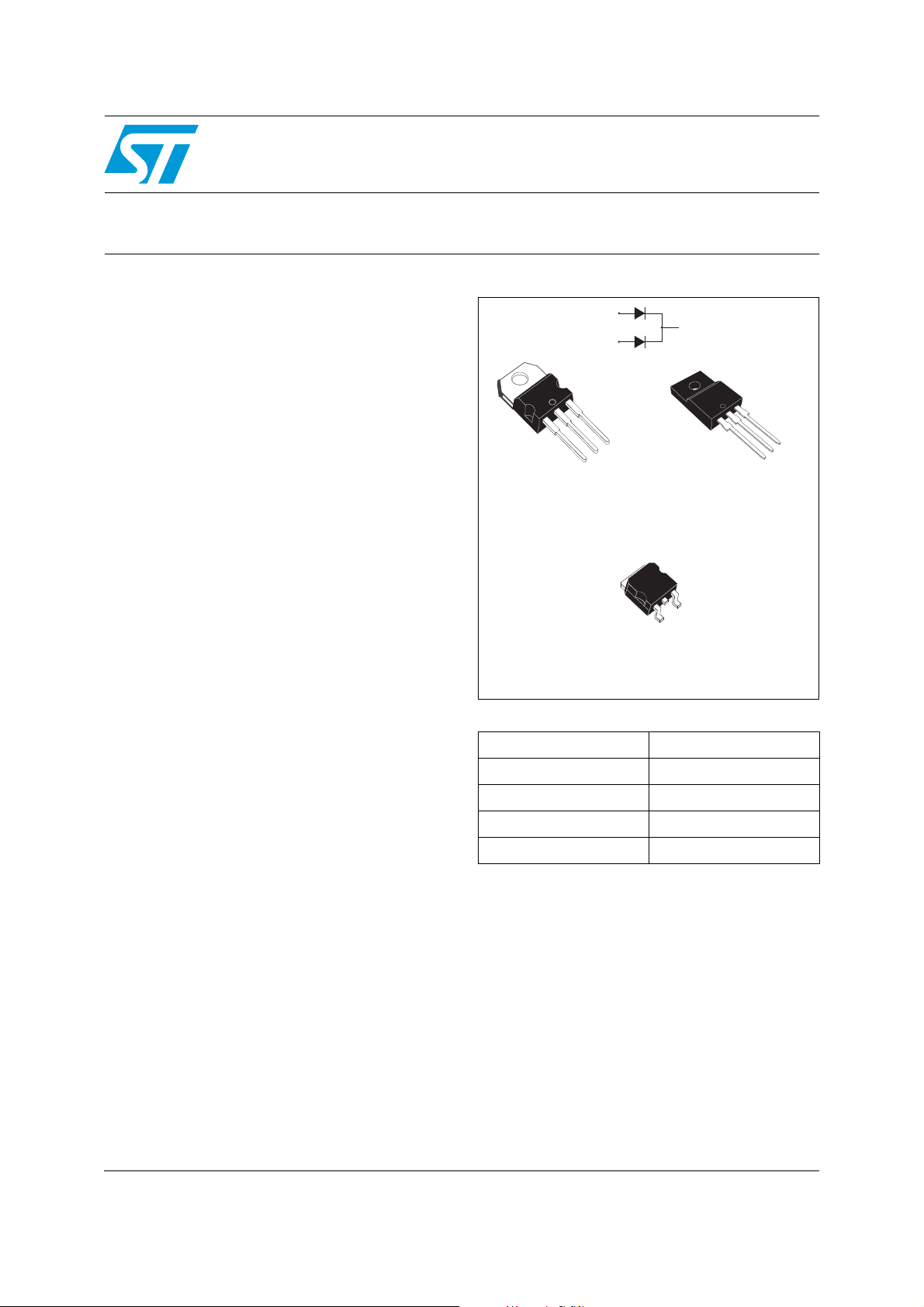
A1
A2
A2
K
A1
TO-220AB
STTH10LCD06CT
STTH10LCD06CFP
K
A1
D2PAK
STTH10LCD06CG-TR
Table 1. Device summary
I
F(AV)
V
RRM
T
j
(typ) 1.25 V
V
F
t
(max) 25 ns
rr
K
TO-220FPAB
A2
2 x 5A
600 V
175 °C
A1
A2
K
April 2011 Doc ID 15897 Rev 3 1/10
www.st.com
10
Page 2
Characteristics STTH10LCD06C
1 Characteristics
Table 2. Absolute ratings
(1)
Symbol Parameter Value Unit
V
I
F(RMS)
I
F(AV)
I
T
1. Limiting values per diode at 25 °C, unless otherwise specified
2. condition to avoid thermal runaway for a diode on its own heatsink
Table 3. Thermal resistance
Repetitive peak reverse voltage 600 V
RRM
Forward current rms 20 A
TO-220AB,
2
PA K
D
Average forward
= 130 °C
T
c
current, δ = 0.5
= 100 °C TO-220FPAB
T
c
Surge non repetitive forward current tp = 10 ms sinusoidal 60 A
FSM
Storage temperature range -65 to + 175 °C
stg
Maximum operating junction temperature
T
j
<
Rth(j-a)
1
dPtot
dTj
(2)
Per diode 5 A
Per device 10 A
Per diode 5 A
Per device 10 A
175 °C
Symbol Parameter Value Unit
2
PA K 4 .5
°C/W
R
Table 4. Static electrical characteristics
Junction to case(per diode)
th(j-c)
TO-220AB, D
TO-220FPAB 7.5
Symbol Parameter Test conditions Min. Typ. Max. Unit
Reverse leakage
(1)
I
R
current
(2)
V
1. Pulse test: tp = 5 ms, δ < 2 %
2. Pulse test: tp = 380 µs, δ < 2 %
Forward voltage drop
F
= 25 °C
T
j
= 150 °C 5 50
T
j
= 25 °C
T
j
T
= 150 °C 1.25 1.6
j
= 25 °C
T
j
T
= 150 °C 1.55 2
j
= V
V
R
I
= 5 A
F
= 10 A
I
F
RRM
1
2
2.35
To evaluate the conduction losses use the following equation:
P = 1.2 x I
F(AV)
+ 0.08 x I
F2(RMS)
µA
V
2/10 Doc ID 15897 Rev 3
Page 3
STTH10LCD06C Characteristics
Table 5. Dynamic electrical characteristics
Symbol Parameter
Test conditions
I
= 0.5 A, Irr = 0.25 A,
F
IR = 1 A, Tj = 25 °C
t
Reverse recovery time
rr
I
V
Reverse recovery current
RM
t
Forward recovery time
fr
Forward recovery voltage
FP
= 1 A, dIF/dt = -50 A/µs,
I
F
= 30 V, Tj = 25 °C
V
R
= 5 A, dIF/dt = -50 A/µs,
I
F
VR = 400 V, Tj = 125 °C
I
= 5 A, dIF/dt = 100 A/µs
F
VFR = 1.1 x V
= 5 A, dIF/dt = 100 A/µs
I
F
= 1.1 x V
V
FR
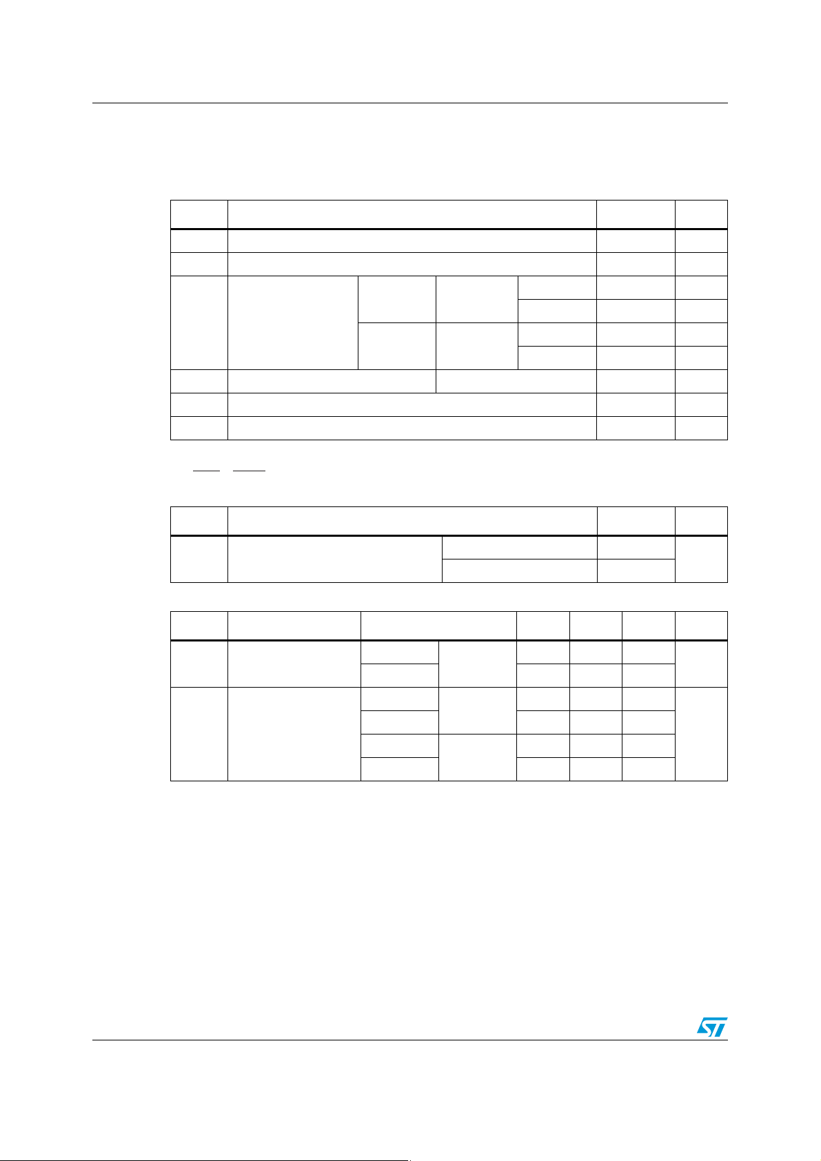
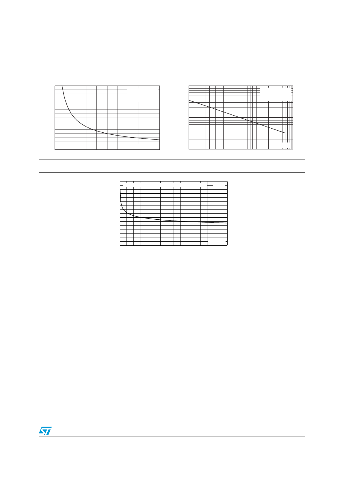
Figure 1. Average forward power dissipation
versus average forward current
(per diode)
P
(W)
F(AV)
12
δ = 0.2
10
8
6
4
2
0
01234567
δ = 0.05
δ = 0.1
I
F(AV)
(A)
δ = 0.5
δ = 1
δ = tp/T
T
t
p
Min. Typ. Max. Unit
25
35 50
1.8 2.5 A
, Tj = 25 °C
Fmax
, Tj = 25 °C
Fmax
5V
100 ns
Figure 2. Forward voltage drop versus
forward current (per diode)
IFM(A)
50
Tj= 150 °C
Tj= 150 °C
(Maximum values)
Tj= 25 °C
(Maximum values)
40
30
20
10
0
(Typical values)
0.0 0.5 1.0 1.5 2.0 2.5 3.0 3.5 4.0
ns
VFM(V)
Figure 3. Relative variation of thermal
impedance junction to case versus
pulse duration (TO-220AB, D
Z
th(j-c)/Rth(j-c)
1.0
TO-220AB
0.9
D2PAK
0.8
0.7
0.6
0.5
0.4
0.3
Single pulse
0.2
0.1
0.0
1.E-04 1.E-03 1.E-02 1.E-01 1.E+00
tp(s)
Figure 4. Relative variation of thermal
impedance junction to case versus
2
PAK)
1.0
0.9
0.8
0.7
0.6
0.5
0.4
0.3
0.2
0.1
0.0
1.E-03 1.E-02 1.E-01 1.E+00 1.E+01
Doc ID 15897 Rev 3 3/10
pulse duration (TO-220FPAB)
Z
th(j-c)/Rth(j-c)
TO-220FPAB
Single pulse
tp(s)
Page 4
Characteristics STTH10LCD06C
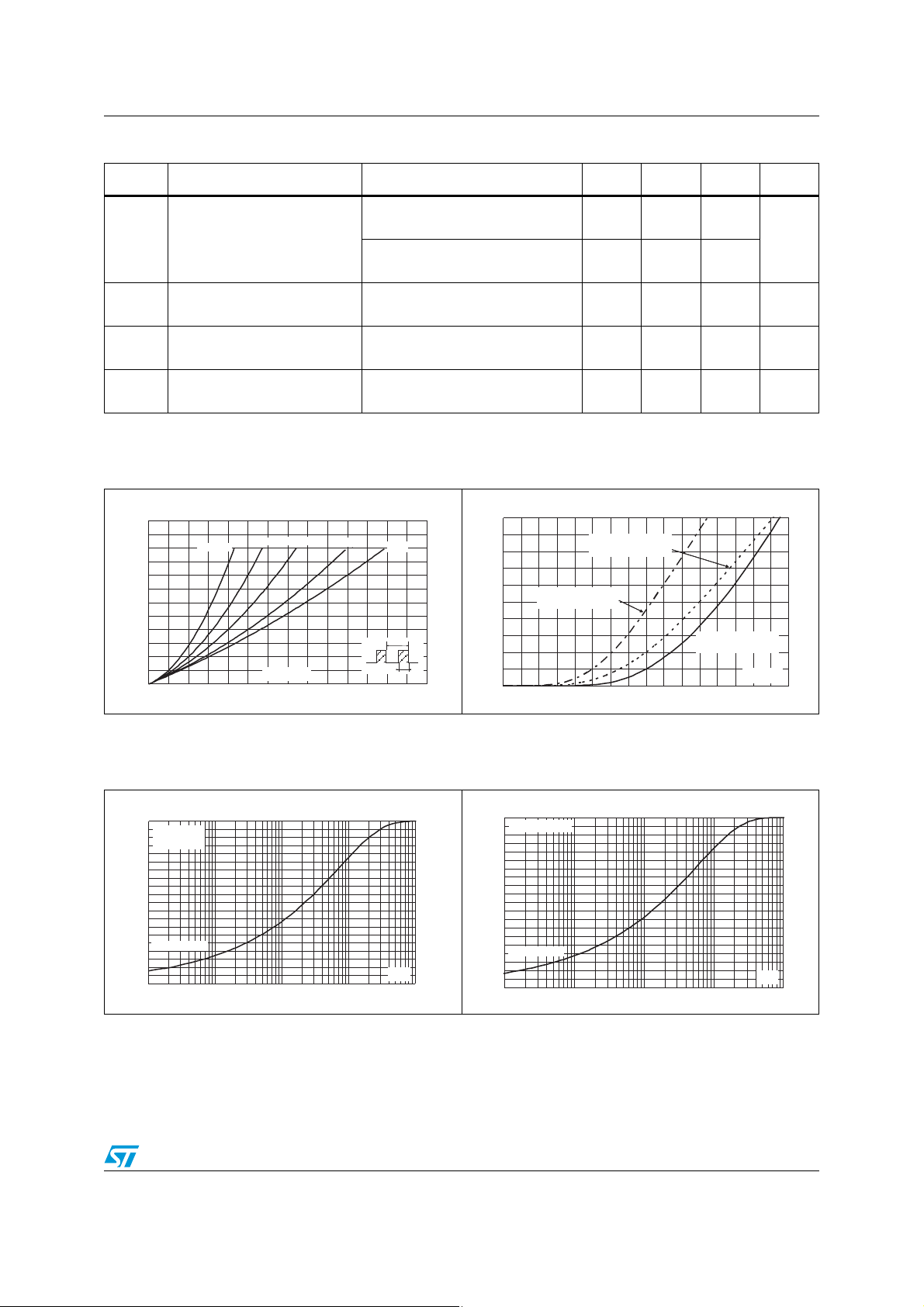
Figure 5. Peak reverse recovery current
versus dI
/dt
F
(typical values, per diode)
IRM(A)
10
IF= I
F(AV)
9
VR= 400 V
Tj= 125 °C
8
7
6
5
4
3
2
1
0
0 50 100 150 200 250 300 350 400 450 500
dIF/dt (A/µs)
Figure 7. Reverse recovery charges versus
/dt (typical values, per diode)
dI
F
QRR(nC)
350
IF= I
F(AV)
VR= 400 V
300
Tj= 125 °C
250
200
150
100
50
0
0 50 100 150 200 250 300 350 400 450 500
dIF/dt (A/µs)
Figure 6. Reverse recovery time versus
dIF/dt (typical values, per diode)
tRR(ns)
200
180
160
140
120
100
80
60
40
20
0
0 50 100 150 200 250 300 350 400 450 500
IF= I
F(AV)
VR= 400 V
Tj= 125 °C
dIF/dt (A/µs)
Figure 8. Reverse recovery softness factor
versus dIF/dt
(typical values, per diode)
S
FAC TOR
5.0
4.5
4.0
3.5
3.0
2.5
2.0
1.5
1.0
0.5
0.0
0 50 100 150 200 250 300 350 400 450 500
IF= I
F(AV)
VR= 400 V
Tj= 125 °C
dIF/dt (A/µs)
Figure 9. Relative variations of dynamic
Figure 10. Transient peak forward voltage
parameters versus junction
temperature
1.2
IF= I
F(AV)
VR= 400 V
1.0
Refernce Tj= 125 °C
0.8
I
0.6
0.4
0.2
0.0
RM
S
FACTOR
Q
RR
25 50 75 100 125
Tj(°C)
4/10 Doc ID 15897 Rev 3
VFP(V)
18
IF= I
16
Tj= 125 °C
14
12
10
8
6
4
2
0
0 50 100 150 200 250 300 350 400 450 500
versus dI
/dt
F
(typical values, per diode)
F(AV)
dIF/dt (A/µs)
Page 5
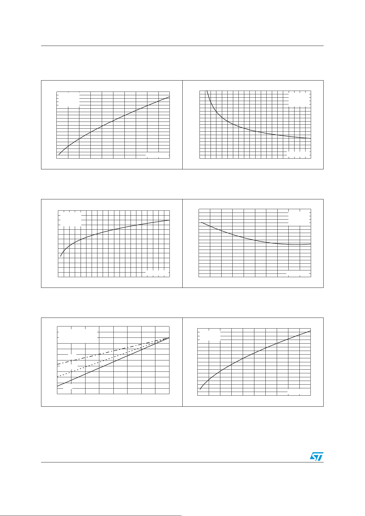
STTH10LCD06C Characteristics
0
Figure 11. Forward recovery time versus dI
(typical values, per diode)
/dt
Figure 12. Junction capacitance versus
F
reverse voltage applied
(typical values, per diode)
tFR(ns)
160
140
120
100
80
60
40
20
0
0 50 100 150 200 250 300 350 400 450 50
IF= I
F(AV)
VR= 1.1 x VFmax.
Tj= 125 °C
dIF/dt (A/µs)
C (pF)
100
V
OSC
10
1
1 10 100 1000
Figure 13. Thermal resistance junction to ambient versus copper surface under tab
R
(°C/W)
th(j-a)
80
Epoxy printed board Fr4, copper thickness: 35 µm
70
60
50
40
30
20
10
0
0 5 10 15 20 25 30 35 40
D2PAK
Scu(cm²)
F = 1 MHz
= 30 mV
Tj= 25 °C
RMS
VR(V)
Doc ID 15897 Rev 3 5/10
Page 6
Package information STTH10LCD06C
2 Package information
● Epoxy meets UL94, V0
● Cooling method: by conduction (C)
● Recommended torque value: 0.4 to 0.6 N·m
In order to meet environmental requirements, ST offers these devices in different grades of
ECOPACK
specifications, grade definitions and product status are available at: www.st.com
ECOPACK
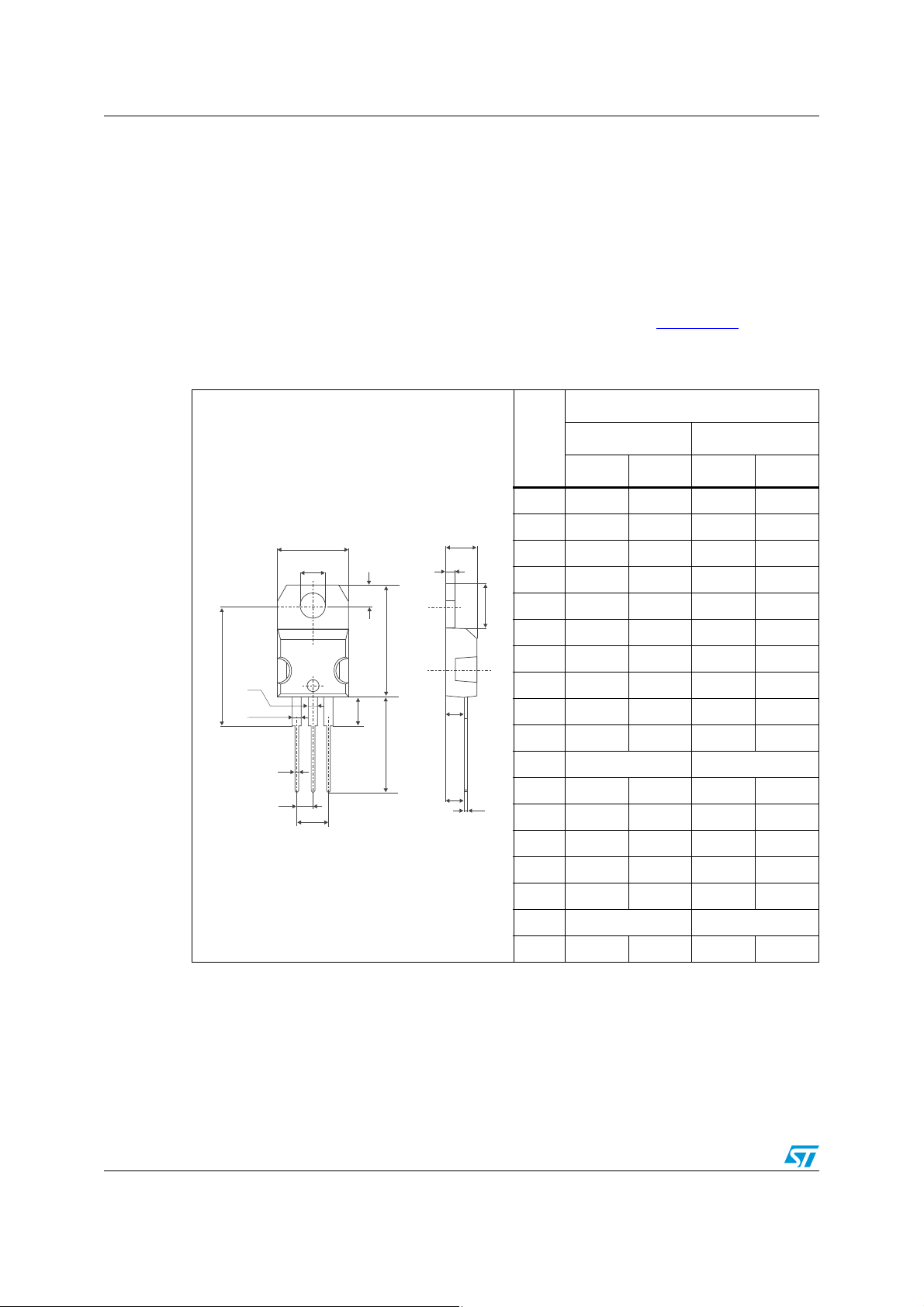
Table 6. TO-220AB dimensions
®
packages, depending on their level of environmental compliance. ECOPACK®
®
is an ST trademark.
.
Dimensions
Ref.
Millimeters Inches
Min. Max. Min. Max.
A 4.40 4.60 0.173 0.181
C 1.23 1.32 0.048 0.051
H2
Dia
A
C
D 2.40 2.72 0.094 0.107
E 0.49 0.70 0.019 0.027
L2
F2
F1
L5
L6
L9
L4
F
G1
L7
F 0.61 0.88 0.024 0.034
F1 1.14 1.70 0.044 0.066
F2 1.14 1.70 0.044 0.066
G 4.95 5.15 0.194 0.202
D
G1 2.40 2.70 0.094 0.106
H2 10 10.40 0.393 0.409
L2 16.4 typ. 0.645 typ.
M
E
L4 13 14 0.511 0.551
L5 2.65 2.95 0.104 0.116
G
L6 15.25 15.75 0.600 0.620
L7 6.20 6.60 0.244 0.259
L9 3.50 3.93 0.137 0.154
6/10 Doc ID 15897 Rev 3
M 2.6 typ. 0.102 typ.
Diam. 3.75 3.85 0.147 0.151
Page 7
STTH10LCD06C Package information
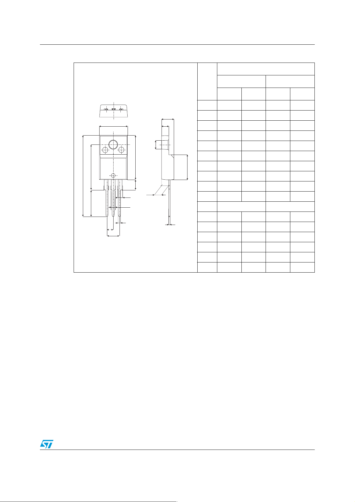
Table 7. TO-220FPAB dimensions
Dimensions
Ref.
Millimeters Inches
Min. Max. Min. Max.
A 4.4 4.6 0.173 0.181
A
H
B
B 2.5 2.7 0.098 0.106
D 2.5 2.75 0.098 0.108
E 0.45 0.70 0.018 0.027
Dia
L6
L2
L3
L5
F1
L4
G1
F2
F
G
D
E
F 0.75 1 0.030 0.039
F1 1.15 1.70 0.045 0.067
F2 1.15 1.70 0.045 0.067
L7
G 4.95 5.20 0.195 0.205
G1 2.4 2.7 0.094 0.106
H 10 10.4 0.393 0.409
L2 16 Typ. 0.63 Typ.
L3 28.6 30.6 1.126 1.205
L4 9.8 10.6 0.386 0.417
L5 2.9 3.6 0.114 0.142
L6 15.9 16.4 0.626 0.646
L7 9.00 9.30 0.354 0.366
Dia. 3.00 3.20 0.118 0.126
Doc ID 15897 Rev 3 7/10
Page 8

Package information STTH10LCD06C
Table 8. D2PAK dimensions
Dimensions
Ref.
Millimeters Inches
Min. Max. Min. Max.
A 4.40 4.60 0.173 0.181
A
L2
E
C2
A1 2.49 2.69 0.098 0.106
A2 0.03 0.23 0.001 0.009
B 0.70 0.93 0.027 0.037
D
L
L3
G
A1
B2
B
C
R
A2
B2 1.14 1.70 0.045 0.067
C 0.45 0.60 0.017 0.024
C2 1.23 1.36 0.048 0.054
D 8.95 9.35 0.352 0.368
E 10.00 10.40 0.393 0.409
G 4.88 5.28 0.192 0.208
L 15.00 15.85 0.590 0.624
M
*
V2
* FLAT ZONE NO LESSTHAN 2mm
L2 1.27 1.40 0.050 0.055
L3 1.40 1.75 0.055 0.069
M 2.40 3.20 0.094 0.126
R 0.40 typ. 0.016 typ.
V2 0° 8° 0° 8°
8/10 Doc ID 15897 Rev 3
Page 9

STTH10LCD06C Ordering information
3 Ordering information
Table 9. Ordering information
Order code Marking Package Weight Base qty. Delivery mode
STTH10LCD06CT STTH10LCD06CT TO-220AB 2.23 g 50 Tube
STTH10LCD06CG-TR STTH10LCD06CG D2PAK 1.48 g 1000 Tape and reel
STTH10LCD06CFP STTH10LCD06C TO-220FPAB 2.04 g 50 Tube
4 Revision history
Table 10. Document revision history
Date Revision Changes
15-Jul-2009 1 First issue.
17-Jan-2011 2 Updated dimensions and graphic in Ta b l e 7 .
07-Apr-2011 3 Added (per diode) in Ta b l e 3 .
Doc ID 15897 Rev 3 9/10
Page 10

STTH10LCD06C
Please Read Carefully:
Information in this document is provided solely in connection with ST products. STMicroelectronics NV and its subsidiaries (“ST”) reserve the
right to make changes, corrections, modifications or improvements, to this document, and the products and services described herein at any
time, without notice.
All ST products are sold pursuant to ST’s terms and conditions of sale.
Purchasers are solely responsible for the choice, selection and use of the ST products and services described herein, and ST assumes no
liability whatsoever relating to the choice, selection or use of the ST products and services described herein.
No license, express or implied, by estoppel or otherwise, to any intellectual property rights is granted under this document. If any part of this
document refers to any third party products or services it shall not be deemed a license grant by ST for the use of such third party products
or services, or any intellectual property contained therein or considered as a warranty covering the use in any manner whatsoever of such
third party products or services or any intellectual property contained therein.
UNLESS OTHERWISE SET FORTH IN ST’S TERMS AND CONDITIONS OF SALE ST DISCLAIMS ANY EXPRESS OR IMPLIED
WARRANTY WITH RESPECT TO THE USE AND/OR SALE OF ST PRODUCTS INCLUDING WITHOUT LIMITATION IMPLIED
WARRANTIES OF MERCHANTABILITY, FITNESS FOR A PARTICULAR PURPOSE (AND THEIR EQUIVALENTS UNDER THE LAWS
OF ANY JURISDICTION), OR INFRINGEMENT OF ANY PATENT, COPYRIGHT OR OTHER INTELLECTUAL PROPERTY RIGHT.
UNLESS EXPRESSLY APPROVED IN WRITING BY AN AUTHORIZED ST REPRESENTATIVE, ST PRODUCTS ARE NOT
RECOMMENDED, AUTHORIZED OR WARRANTED FOR USE IN MILITARY, AIR CRAFT, SPACE, LIFE SAVING, OR LIFE SUSTAINING
APPLICATIONS, NOR IN PRODUCTS OR SYSTEMS WHERE FAILURE OR MALFUNCTION MAY RESULT IN PERSONAL INJURY,
DEATH, OR SEVERE PROPERTY OR ENVIRONMENTAL DAMAGE. ST PRODUCTS WHICH ARE NOT SPECIFIED AS "AUTOMOTIVE
GRADE" MAY ONLY BE USED IN AUTOMOTIVE APPLICATIONS AT USER’S OWN RISK.
Resale of ST products with provisions different from the statements and/or technical features set forth in this document shall immediately void
any warranty granted by ST for the ST product or service described herein and shall not create or extend in any manner whatsoever, any
liability of ST.
ST and the ST logo are trademarks or registered trademarks of ST in various countries.
Information in this document supersedes and replaces all information previously supplied.
The ST logo is a registered trademark of STMicroelectronics. All other names are the property of their respective owners.
© 2011 STMicroelectronics - All rights reserved
STMicroelectronics group of companies
Australia - Belgium - Brazil - Canada - China - Czech Republic - Finland - France - Germany - Hong Kong - India - Israel - Italy - Japan -
Malaysia - Malta - Morocco - Philippines - Singapore - Spain - Sweden - Switzerland - United Kingdom - United States of America
www.st.com
10/10 Doc ID 15897 Rev 3
 Loading...