


STG719
LOW VOLTAGE 4Ω SPDT SWITCH
■ HIGH SPEED:
t
= 0.3ns (TYP.) at VCC = 5V
PD
t
= 0.4ns (TYP.) at VCC = 3.3V
PD
■ LOW POWER DISSIPATION:
I
= 1µA(MAX.) at TA=25°C
CC
■ LOW "ON" RESISTANCE:
R
= 4Ω (MAX. TA=25°C) AT VCC = 5V
ON
R
= 6Ω (TYP.) AT VCC = 3V
ON
■ WIDE OPERATING VOLTAGE RANGE:
V
(OPR) = 1.8V TO 5.5V SINGLE SUPPLY
CC
DESCRIPTION
The STG719 is an high-speed S.P.D.T. (Single
Pole Double Throw) SWITCH fabricated in silicon
gate C
2
MOS technology. It designed to operate
from 1.8V to 5.5V, making this device ideal for
portable applications, audio signal ro uting, video
switching, mobile and communicat ion system s.
It offers 4Ω ON-Resistance Max at 5V 25°C and
very low ON-Resistance Flatness. Addition al key
features are fast switching speed (t
ON
=7ns,
SOT23-6L
Table 1: Order Codes
PACKAGE T & R
SOT23-6L STG719STR
t
=4.5ns), Break Before Make Delay Time a nd
OFF
Low Power Consumption.
All inputs and outputs are equipped with
protection circuits against static disc harge, giving
them ESD immunity and transient excess voltage.
It’s available in the commercial and extended
temperature range.
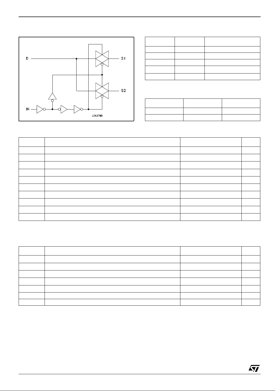
Figure 1: Pin Connection An d I E C Logic Symbols
Rev. 8
1/10November 2004
STG719
Figure 2: Input Equivalent Circuit Table 2: Pin Description
PIN N° SYMBOL NAME AND FUNCTION
1 IN Control
4, 6 S1, S2 Independent Channel
5 D Common Channel
2
3 GND Ground (0V)
TRUTH TABLE
IN SWITCH S1 SWITCH S2
LONOFF
HOFFON
Table 3: Absolute Maximum Ratings
Symbol Parameter Value Unit
V
V
V
V
I
I
OK
I
I
or I
CC
T
T
Absolute Maximum Ratings are those values beyond which damage to the device may occur. Functional operation under these conditions is
not implied
Supply Voltage
CC
DC Input Voltage -0.5 to VCC + 0.5
I
DC Control Input Voltage -0.5 to VCC + 0.5
IC
DC Output Voltage -0.5 to VCC + 0.5
O
DC Input Diode Current
IK
DC Output Diode Current
DC Output Current
O
DC VCC or Ground Current
GND
Storage Temperature
stg
Lead Temperature (10 sec)
L
Table 4: Recommended Operating Conditions
V
CC
Positive Supply Voltage
-0.5 to +7.0 V
± 20 mA
± 20 mA
± 50 mA
± 50 mA
-65 to +150 °C
300 °C
V
V
V
Symbol Parameter Value Unit
V
V
V
V
T
Supply Voltage (note 1)
CC
Input Voltage 0 to V
I
Control Input Voltage 0 to V
IC
Output Voltage 0 to V
O
Operating Temperature
op
1.8 to 5.5 V
CC
CC
CC
-55 to 125 °C
dt/dv Input Rise and Fall Time on control pin (note 2) 0 to 10 ns/V
dt/dv Input Rise and Fall Time on I/O pins 0 to DC ns/V
1) Truth T abl e guarante ed: 1.2V to 6V
2) VIN from 30 % t o 70% of V
CC
2/10
V
V
V

Table 5: DC Specifications
Symbol Parameter
V
V
R
∆R
R
FLATON
I
SOFF
I
IHC
ILC
ON
ON
SON
I
IN
I
CC
High Level Control
Input Voltage
Low Level Control
Input Voltage
ON Resistance
ON Resistance
ON Resistance
fLATNESS
Source OFF
Leakage
Channel ON
Leakage
Control Input
Leakage Current
Quiescent Supply
Current
V
3.3
5.0
3.3
5.0
3.3
5.0
3.3
5.0
3.3
5.0
3.3
5.0
3.3
5.0
3.3
5.0
3.3
5.0
Test Condition Value
= 25°C
T
CC
(V)
(*)
(**)
(*)
(**)
(*)
VS = 0 to VCC
(**)
(*)
(**)
(*)
(**)
(*)
(**)
(*)
(**)
(*)
(**)
(*)
(**)
I
S
VS = 0 to VCC
I
S
VS = 0 to VCC
I
S
VS =1V or VCC
V
= VCC or 1V
DD
V
= VCC or GND
IN
VS=VD=1V to VCC-2.5V
VIN = V
VI = VIH or V
VI = VCC or GND
= 10mA
= 10mA
= 10mA
IHC
IL
A
Min. Typ. Max. Min. Max. Min. Max.
2.0 2.0 2.0
2.4 2.4 2.4
0.4 0.4 0.4
0.8 0.8 0.8
67 10 12
456
0.1 0.4
0.1 0.4
2.5
0.75
±0.01 ±0.25
±0.01 ±0.25
±0.01 ±0.25
±0.01 ±0.25
0.005
0.005
0.001 1 1 2
0.001 1 2
STG719
-40 to 85°C -55 to 125°C
±
0.35
±
0.35
±
0.35
±
0.35
±0.1 ±1
±0.1
±
±
±
±
3.5
3.5
3.5
3.5
±1
Unit
V
V
Ω
Ω
Ω
nA
nA
µA
µA
(*) Voltage range is 3.3V ± 0.3V
(**) Voltage range is 5V ± 0.5V
3/10

STG719
Table 6: AC Electrical Characteristics (CL = 35pF, RL = 300Ω)
Test Condition Value
= 25°C
Symbol Parameter
t
Delay Time
PD
ON
OFF
t
D
SOFF
SON
ON Channel Time
OFF Channel Time
Break Before Make
Time Delay
OFF Channel
Capacitance
ON Channel
Capacitance
0.5V
t
t
C
C
(*) Voltage range is 3.3V ± 0.3V
(**) Voltage range is 5.0V ±
V
3.3
5.0
3.3
5.0
3.3
5.0
3.3
5.0
(V)
CC
(*)
(**)
(*)
(**)
(*)
(**)
(*)
(**)
VS = 3V square
wave f = 1MHz
tr = tf = 6ns
VS = 2V
VS = 3V
VS = 2V
VS = 3V
VS = 2V
VS = 3V
T
A
Min. Typ. Max. Min. Max. Min. Max.
0.4 0.8 1.2 2.4
0.3 0.6 1.0 2.0
10 16 19
71113
5.5 7 8.5
4.5 6 7.5
14
14
19 pF
33 pF
-40 to 85°C -55 to 125°C
Unit
ns
ns
ns
ns
Table 7: Analog Switch Characteristics (GND = 0V; TA = 25°C)
Test Condition Value
Symbol Parameter
f
MAX
Frequency Response
(Switch ON)
Feed through
Attenuation (Switch
OFF)
Crosstalk (Control
Input to Signal
Output)
(*)Voltage range is 3.3V ± 0.3V
(**) Voltage range is 5.0V ±
0.5V
V
3.3
5.0
3.3
3.3
5.0
5.0
3.3
3.3
5.0
5.0
CC
(V)
(*)
(**)
(*)
(*)
(**)
(**)
(*)
(*)
(**)
(**)
Bandwidth at -3dB
fIN = 10MHz sine wave -40
fIN = 1MHz sine wave -74
fIN = 10MHz sine wave -40
fIN = 1MHz sine wave -74
fIN = 10MHz sine wave -39
fIN = 1MHz sine wave -52
fIN = 10MHz sine wave -39
fIN = 1MHz sine wave -52
Typ.
200
200
Unit
MHz
dB
dB
4/10

TEST CIRCUITS
STG719
Figure 3: On Resistance
Figure 4: On Leakage
Figure 6: Off Isolation
Figure 7: Bandwi dth
Figure 5: Off Leakage
Figure 8: Channel To Channel Crosstalk
5/10

STG719
Figure 9: Switching Times
Table 8: Break Before Make Time Delay
6/10

STG719
SOT23-6L MECHANICAL DATA
mm. mils
DIM.
MIN. TYP MAX. MIN. TYP. MAX.
A 0.90 1.45 35.4 57.1
A1 0.00 0.15 0.0 5.9
A2 0.90 1.30 35.4 51.2
b 0.35 0.50 13.7 19.7
C 0.09 0.20 3.5 7.8
D 2.80 3.00 110.2 118.1
E 2.60 3.00 102.3 118.1
E1 1.50 1.75 59.0 68.8
e.95 37.4
e1 1.9 74.8
L 0.35 0.55 13.7 21.6
0
7/10

STG719
Tape & Reel SOT23-xL MECHANICAL DATA
DIM.
MIN. TYP MAX. MIN. TYP. MAX.
A 180 7.086
C 12.8 13.0 13.2 0.504 0.512 0.519
D 20.2 0.795
N 60 2.362
T 14.4 0.567
Ao 3.13 3.23 3.33 0.123 0.127 0.131
Bo 3.07 3.17 3.27 0.120 0.124 0.128
Ko 1.27 1.37 1.47 0.050 0.054 0.0.58
Po 3.9 4.0 4.1 0.153 0.157 0.161
P 3.9 4.0 4.1 0.153 0.157 0.161
mm. inch
8/10

Table 9: Revision History
Date Revision Description of Change s
25-Nov-2004 8 Mistake on Figure 1.
STG719
9/10

STG719
Information furnished is believed to be accurate and reliable. However, STMicroelectronics assumes no responsibility for the consequences
of use of s uch inf ormati on nor for a ny infr ing eme nt o f p atent s or o ther ri ghts of third parties which may resul t fr om its us e. No lic ens e is gr an ted
by implication or otherwise under any patent or patent rights of STMicroelectronics. Specifications mentioned in this publication are subject
to change without notice. This publication supersedes and replaces all information previously supplied. STMicroelectronics produ cts are not
authorized for use as critical components in life support devices or systems without express written approval of STMicroelectronics.
The ST logo is a registered trademark of STMicroelectronics
All other names are the property of their respective owners
© 2004 STMicroelectronics - All Rights Reserved
STMicroelectronics group of companies
Australia - Belgium - Brazil - Canada - China - Czech Republic - Finland - France - Germany - Hong Kong - India - Israel - Italy - Japan -
Malaysia - Malta - Morocco - Singapore - Spain - Sweden - Switzerland - United Kingdom - United States of America
www.st.com
10/10
 Loading...