


Features
■ IC front panel controller/driver
■ Timing power standby management controller
■ IC power supply from 3.3V (V
■ Integrated VFD driver and controller
■ Infrared (IR) Remote Control (RC) Decoder
(Philips or NEC format)
■ Drives many display modes (12 segments/16
digits to 20 segments/8 digits)
■ High voltage outputs (V
■ No external resistors necessary for driver
DD
outputs (P-channel open- drain with pull-down
resistor outputs)
■ Key scanning (up to 12mm x 2mm matrix)
■ Led ports (4 channels, 20mA, max)
■ Serial interface (STB, CLK, D
communication protocol
■ Dimming circuit (adjustable up to 8 steps)
■ Supports auto-increment of display digit, which
lightens the load on the MCU
■ Programmable 8 hot keys for the IR remote
control command
■ Programmable 8 hot keys for key scan
command
■ Low power consumption in standby mode
■ 2 general purpose input ports (SW1, SW2)
■ Available in PQFP-52 package
) to –30V (VSS)
DD
- 33.3V max)
, and D
IN
OUT
)
STFPC311
Front panel controller/driver
with standby power management
PQFP-52
Description
The STFPC311 is a complete, low-cost,
integrated solution for controlling and driving a
front panel Vacuum Fluorescent Display (VFD). It
is ideal for decreasing power consumption in
standby mode by reducing the application standby
current to a minimum. It also contains a built-in
remote control decoder module.
While in the standby mode of operation, a valid
key press or signal from infrared decoder will start
a proper power-up see Figure 6 on page 12.
The STFPC311 integrates a VFD controller with a
driver that is run on a 1/8 to 1/16-duty factor. It
consists of 12 segments output lines, 8 grid output
lines, 8 shared segments/grid output drive lines, a
display memory, a control circuit, and a key scan
circuit. Serial data is input to the STFPC311
through the SPI Interface of a microcontroller
(STB, D
Additionally, this IC can support 2 general
purpose input switches (SW1 and SW2).
Features
, D
IN
, and CLK).
OUT
■ DVD players
■ VCD players
■ AV equipment like Home Stereo
■ POS Systems
Order Codes
Part number Temperature range Package
STFPC311 -40 to 85°C PQFP-52
May 2006 Rev 1 1/39
www.st.com
39

STFPC311
Contents
1 Functional description . . . . . . . . . . . . . . . . . . . . . . . . . . . . . . . . . . . . . . . . . 4
1.1 Block diagram . . . . . . . . . . . . . . . . . . . . . . . . . . . . . . . . . . . . . . . . . . . . . . . . . 4
2 Pin connection . . . . . . . . . . . . . . . . . . . . . . . . . . . . . . . . . . . . . . . . . . . . . . . . 5
2.1 Pin description . . . . . . . . . . . . . . . . . . . . . . . . . . . . . . . . . . . . . . . . . . . . . . . . 6
3 Initialization . . . . . . . . . . . . . . . . . . . . . . . . . . . . . . . . . . . . . . . . . . . . . . . . . . 7
3.1 Normal mode of operation . . . . . . . . . . . . . . . . . . . . . . . . . . . . . . . . . . . . . . . 7
3.2 Receive operation . . . . . . . . . . . . . . . . . . . . . . . . . . . . . . . . . . . . . . . . . . . . . . 7
3.3 Transmit operation . . . . . . . . . . . . . . . . . . . . . . . . . . . . . . . . . . . . . . . . . . . . . 7
3.4 Standby or power-down mode . . . . . . . . . . . . . . . . . . . . . . . . . . . . . . . . . . . . 8
3.5 IR Decoding . . . . . . . . . . . . . . . . . . . . . . . . . . . . . . . . . . . . . . . . . . . . . . . . . . 8
3.6 Watchdog timer . . . . . . . . . . . . . . . . . . . . . . . . . . . . . . . . . . . . . . . . . . . . . . . . 8
3.6.1 Watchdog timer operation during power-up . . . . . . . . . . . . . . . . . . . . . . . . . . . 9
3.6.2 Watchdog timer operation during power-down . . . . . . . . . . . . . . . . . . . . . . . 10
3.6.3 Watchdog timer operation during standby . . . . . . . . . . . . . . . . . . . . . . . . . . . 11
3.7 Flow charts . . . . . . . . . . . . . . . . . . . . . . . . . . . . . . . . . . . . . . . . . . . . . . . . . 12
4 Display RAM address and display mode . . . . . . . . . . . . . . . . . . . . . . . . . . 15
5 Data . . . . . . . . . . . . . . . . . . . . . . . . . . . . . . . . . . . . . . . . . . . . . . . . . . . . . . . . 17
5.1 LED Port . . . . . . . . . . . . . . . . . . . . . . . . . . . . . . . . . . . . . . . . . . . . . . . . . . . . 17
5.2 SW Data . . . . . . . . . . . . . . . . . . . . . . . . . . . . . . . . . . . . . . . . . . . . . . . . . . . . 17
6 Commands . . . . . . . . . . . . . . . . . . . . . . . . . . . . . . . . . . . . . . . . . . . . . . . . . . 18
6.1 Configuration mode setting command . . . . . . . . . . . . . . . . . . . . . . . . . . . . . 18
6.2 Data setting command . . . . . . . . . . . . . . . . . . . . . . . . . . . . . . . . . . . . . . . . . 19
6.3 Address setting command . . . . . . . . . . . . . . . . . . . . . . . . . . . . . . . . . . . . . . 20
6.4 Display control and hotkey setting command . . . . . . . . . . . . . . . . . . . . . . . . 20
7 Programmable hotkeys . . . . . . . . . . . . . . . . . . . . . . . . . . . . . . . . . . . . . . . . 22
7.1 IR Remote control . . . . . . . . . . . . . . . . . . . . . . . . . . . . . . . . . . . . . . . . . . . . . 22
7.2 Front panel keys . . . . . . . . . . . . . . . . . . . . . . . . . . . . . . . . . . . . . . . . . . . . . . 22
2/39

STFPC311
8 Default status . . . . . . . . . . . . . . . . . . . . . . . . . . . . . . . . . . . . . . . . . . . . . . . . 24
8.1 Power-up default status . . . . . . . . . . . . . . . . . . . . . . . . . . . . . . . . . . . . . . . . . 24
8.2 STANDBY status . . . . . . . . . . . . . . . . . . . . . . . . . . . . . . . . . . . . . . . . . . . . . . 24
9 Remote control protocols . . . . . . . . . . . . . . . . . . . . . . . . . . . . . . . . . . . . . . 25
9.1 RC-5 remote control . . . . . . . . . . . . . . . . . . . . . . . . . . . . . . . . . . . . . . . . . . . 25
9.2 SPI interface IR data transmission . . . . . . . . . . . . . . . . . . . . . . . . . . . . . . . . 26
9.3 NEC remote control . . . . . . . . . . . . . . . . . . . . . . . . . . . . . . . . . . . . . . . . . . . 26
10 Maximum rating . . . . . . . . . . . . . . . . . . . . . . . . . . . . . . . . . . . . . . . . . . . . . . 28
10.1 Power consumption estimation . . . . . . . . . . . . . . . . . . . . . . . . . . . . . . . . . . . 29
11 Electrical characteristics . . . . . . . . . . . . . . . . . . . . . . . . . . . . . . . . . . . . . . 30
12 Timing characteristics . . . . . . . . . . . . . . . . . . . . . . . . . . . . . . . . . . . . . . . . 31
13 Serial communication format . . . . . . . . . . . . . . . . . . . . . . . . . . . . . . . . . . . 32
14 Typical application diagram . . . . . . . . . . . . . . . . . . . . . . . . . . . . . . . . . . . . 35
15 Package mechanical data . . . . . . . . . . . . . . . . . . . . . . . . . . . . . . . . . . . . . . 36
16 Revision history . . . . . . . . . . . . . . . . . . . . . . . . . . . . . . . . . . . . . . . . . . . . . . 38
3/39

1 Functional description STFPC311
1 Functional description
The STFPC311 receives serial data from the microcontroller through the SPI interface, latches
the data, and then masks the inputs from the MCU. This data consists of commands followed
by data. There are 4 types of commands:
● configuration,
● data,
● address, and
● display.
The STFPC311 integrates the supply standby power management functionality, remote control
decoder, and a 28-bit VFD driver. Microcontrollers usually run the first two tasks.
This device reduces the stand-by power consumption of the whole Front Panel application as
well as the hardware by integrating the infrared (IR) remote control decoder.
A dedicated supply voltage powers the STFPC311 directly from the main supply board. When
power is plugged in, control of the power supply management is done using the following pins:
1. STBY,
2. IR_DATA_IN, and
3. READY.
1.1 Block diagram
Figure 1. Block diagram
IR_ DATA_ IN
IR_ DATA_ IN
IR_ DATA_ IN
READY/STBY_n
READY/STBY_n
READY/STBY_n
D
D
D
IN
IN
IN
D
D
D
OUT
OUT
OUT
CLK
CLK
CLK
STB
STB
STB
V
V
V
DD
DD
DD
R
R
R
OSC
OSC
OSC
SW1
SW1
SW1
SW2
SW2
SW2
KEY1
KEY1
KEY1
KEY2
KEY2
KEY2
2
2
2
Seri al
Seri al
Seri al
OSC
OSC
OSC
2-bit
2-bit
2-bit
Lat ch
Lat ch
Lat ch
SPI
SPI
SPI
I/F
I/F
I/F
Remote Control
Remote Control
Remote Control
Decoder & Stand
Decoder & Stand
Decoder & Stand
By Function
By Function
By Function
Command Decod er
Command Decod er
Command Decod er
Display Memory
Display Memory
Display Memory
(20 x 16)
(20 x 16)
(20 x 16)
Timing Generator
Timing Generator
Timing Generator
Key Scan and
Key Scan and
Key Scan and
Dimmi ng Circuit
Dimmi ng Circuit
Dimmi ng Circuit
Key Dat a Memor y
Key Dat a Memor y
Key Dat a Memor y
(2 x 12)
(2 x 12)
(2 x 12)
2
2
2
Lat ch
Lat ch
Lat ch
4-bit
4-bit
4-bit
LED1
LED1
LED1
LED2
LED2
LED2
LED3
LED3
LED3
LED4
LED4
LED4
STBY
STBY
STBY
MUTE
MUTE
MUTE
20-bit
20-bit
20-bit
Out put
Out put
Out put
Lat ch
Lat ch
Lat ch
16-bit
16-bit
16-bit
Shift
Shift
Shift
Regis ter
Regis ter
Regis ter
V
V
V
DD
DD
DD
(+3.3V)
(+3.3V)
(+3.3V)
GND
GND
GND
(0V)
(0V)
(0V)
Watchdog
Watchdog
Watchdog
Timer
Timer
Timer
20 12
20 12
20 12
8
8
8
Dat a
Dat a
Dat a
Selec tor
Selec tor
Selec tor
8
8
8
16
16
16
V
V
V
SS
SS
SS
(-30V)
(-30V)
(-30V)
SEG1/KS1
SEG1/KS1
SEG1/KS1
Dri vers
Dri vers
Dri vers
Segment
Segment
Segment
8
8
8
Multiplexed
Multiplexed
Multiplexed
Gri d
Gri d
Gri d
8
8
8
Dri vers
Dri vers
Dri vers
Dri vers
Dri vers
Dri vers
SEG12/KS2
SEG12/KS2
SEG12/KS2
SEG13/GRID16
SEG13/GRID16
SEG20/GRID9
SEG20/GRID9
SEG20/GRID9
GRID8
GRID8
GRID8
GRID1
GRID1
GRID1
4/39

STFPC311 2 Pin connection
2 Pin connection
Figure 2. Connection diagram (top view PQFP-52)
STFPC311
Note: For a description of the behavior of each pin, refer to the Table 1: Pin description on page 6.
5/39

2 Pin connection STFPC311
2.1 Pin description
Table 1. Pin description
Pin Nº Symbol Type Name and function
1 OSC I This is the oscillator input pin. Connect this pin to an external resistor.
2, 3 SW1, SW2 I General purpose switch input ports.
4MUTEO
5S TBY O
7 GND POWER Connect this pin to system GND.
High level indicates mute status for audio. Low level indicates normal
working.Note 1
there is a typo. Pin5 and name is STBY. Standby output to put the MCU
in low power mode.
It is a command to the main power board. High level indicates stand-by
status. Low level indicates normal working. Note 1
8, 9 KEY1, KEY2 I
Input data to these pins from external keyboard are latched at end of
the display cycle (maximum keyboard size is 12 x 2).
High level on this pin means that main board chip has been working
10 READY I
normally.Note 1 This pin should never float. It is recommended have a
pull-down resistor on this input.
1 IR_DATA_IN I Remote control input. Feeds the IR data from photodiode to this pin.
14 to 25
12, 26
27 to 34
SEG1/KS1 to
SEG12/KS12
V
SS
SEG13/GRID16
to SEG20/GRID9
O Segment output pins (dual function as key source).
V
POWER
outputs high voltage pull-down level. VDD--33.3V max.
FD
O These pins are selectable for segment or grid driving.
35 to 37 GRID8 to GRID6 O Grid output pins.
6, 13,38
V
DD
POWER 3.3V ± 0.3V Core main supply voltage.
39 NC O Not used. Left unconnected.
40 to 44 GRID5 to GRID1 O Grid output pins.
Initializes the serial interface at the rising or falling edge to make the
STFPC31 wait for reception of command. The data input after the falling
45 STB I
edge of STB is processed as a command. While the command data is
processed, current processing is stopped, and the serial interface is
initialized. While STB is high, CLK is ignored and any instruction from
the MCU is neglected.
46 CLK I
Reads serial data at the rising edge, and outputs data at the falling
edge.
47
48
49-52
D
IN
D
OUT
LED1, LED2,
LED3, LED4
O
O CMOS outputs (20mA, max).
Inputs serial data at the rising edge of the shift clock, starting from the
I
lower bit.
Outputs serial data at the faling edge of the shift clock, starting from the
lower bit. This is the N-channel opendrain output pin.
Note: 1 For a detailed behavioral description of these pins, refer to the “STFPC311 Timing Power
Stand-by Sequencer Flow-Chart”. See Table 6 on page 12
6/39

STFPC311 3 Initialization
3 Initialization
After the power is plugged in, the device will supply power to all of the components (including
the host processor) by setting STBY to logic low in order to allow the host processor to program
the STFPC311. Once the STBY is set to low, the watchdog timer starts to count up to 10s (10s
is the default value of the watchdog timer upon power-up). When the READY is asserted within
this time, it indicates that the system has booted up well. If the READY pin is not asserted (logic
high) within this time (10s), the STFPC311 will put the system into standby mode again by
setting STBY to logic high.
If READY is detected as logic high, the watchdog timer will be turned OFF. The main processor
should program the remote control hot key and initialize the other parameters of the STFPC311
in preparation for normal operation before the system goes into standby mode. After all of the
STFPC311 configuration is finished, the host processor may set the READY to low so that the
STFPC311 enters standby mode. The STFPC311 then sets the MUTE pin to logic high to mute
the audio output as well as the STBY pin to logic high. As a consequence of this action, the
main supply voltage is turned off.
3.1 Normal mode of operation
After the power is plugged in, the device will supply power to all of the components (including
the host processor) by setting STBY to logic low in order to allow the host processor to program
the STFPC311. Once the STBY is set to low, the watchdog timer starts to count up to 10s (10s
is the default value of the watchdog timer upon power-up). When the READY is asserted within
this time, it indicates that the system has booted up well. If the READY pin is not asserted (logic
high) within this time (10s), the STFPC311 will put the system into standby mode again by
setting STBY to logic high.
If READY is detected as logic high, the watchdog timer will be turned OFF. The main processor
should program the remote control hot key and initialize the other parameters of the STFPC311
in preparation for normal operation before the system goes into standby mode. After all of the
STFPC311 configuration is finished, the host processor may set the READY to low so that the
STFPC311 enters standby mode. The STFPC311 then sets the MUTE pin to logic high to mute
the audio output as well as the STBY pin to logic high. As a consequence of this action, the
main supply voltage is turned off.
3.2 Receive operation
In receive condition, the STFPC311 waits for a valid command from the MCU. The receive
circuit of STFPC311 receives 8 bit serial data, latches the data and then masks the inputs from
the MCU. Refer to Figure 28 on page 32 for receive timing.
3.3 Transmit operation
In transmit condition, the STFPC311 sends the 8-bit serial data (LSB transmitted first)
whenever a key is pressed or IR data is received. STFPC311 transmits data on the falling edge
of CLK. Refer to Figure 29 on page 32 for transmit timing.
7/39

3 Initialization STFPC311
3.4 Standby or power-down mode
Once the STFPC311 detects the status change of the READY to a logic low or after the preset
waiting time (1s to 15s) has elapsed, the STFPC311 sets the STBY pin to a logic high to turn off
the power. The MUTE signal is set to high before the power is turned off. The STFPC311
always senses the level on the READY pin during normal operation.
3.5 IR Decoding
Encoded IR data from photodiode is supplied to the IR_DATA_IN input pin. The data is
decoded by the internal remote control decoder module of STFPC311. In standby mode, the
remote control decoder recognizes a set of predefined commands (such as STANDBY, PLAY,
and OPEN/CLOSE), and takes appropriate action to manage the power supply.
These predefined commands are known as "hot keys" and are programmable. The decoded IR
commands are passed on to the main processor through the SPI interface by sending 3 bytes
of data on the D
OUT
pin.
3.6 Watchdog timer
The watchdog timer is used to detect an out-of-control microprocessor. The watch dog timer is
implemented in the STFPC311 to detect the abnormal processor behavior or processor-hung
condition. The default state of the watchdog timer is 10s when the device powers-up. It is
initialized by writing to the watchdog register and can be programmed to up to 15s (4-bit
watchdog timer, present in the configuration mode setting command).
If the processor does not reset the timer within the specified period, the STFPC311 will put the
entire system into standby mode to reset the appliance that has stopped abnormally. The action
to take when the watchdog timer has reached its count is to set the Watchdog Action register.
The watchdog timer can be reset by the host processor by sending a command to reset the
watchdog timer. The time-out period then starts over again. If the processor needs to be reset
as a result of a hung condition (signalled using the STBY output of the STFPC311), the
watchdog timer uses the amount of the time-out programmed into the Watchdog Register by
the user to generate an interrupt.
Note: The accuracy of the timer is within ±10% the selected resolution. This depends on the value of
the external bias resistor, as it determines the internal clock frequency.
The watchdog function is automatically set to 10s upon power-up and the Watchdog Interrupt is
cleared. This boot-up watchdog timer is used to make sure that if the host processor hangs
during the first boot-up, the STFPC311 will put the system to standby mode. During the first
boot-up, the watchdog timer is disabled after the first READY signal is received.
8/39

STFPC311 3 Initialization
3.6.1 Watchdog timer operation during power-up
Figure 3. Power-up condition
Note: Watchdog timer is turned off by default upon READY assertion.
If Watchdog is to be kept on during READY high condition, the WDG registers must be set
accordingly by proper commands through SPI bus.
In this power-up condition, the watchdog timer is triggered by internal POR pulse.
During power-up, the watchdog timer value is 10s.
9/39

3 Initialization STFPC311
3.6.2 Watchdog timer operation during power-down
Figure 4. Power-down condition
Note: The watchdog timer can be kept on during normal conditions when READY is high (depending
on the user’s settings).
In this condition, the watchdog timer can be disabled or enabled. If the watchdog timer is
enabled, the timer needs to be cleared before the programmed count of the timer is reached. If
the programmed count is reached, the STBY will be asserted.
Caution: It is advisable not to enable the watchdog timer during normal operation.
10/39

STFPC311 3 Initialization
3.6.3 Watchdog timer operation during standby
● When a hot-key signal is detected either from the front panel or remote control during
standby, the STBY de-asserts.
● The de-assertion of the STBY triggers the watchdog timer.
● The timer value is the programmed value that is set by the user (1s-15s). If the user did not
change the value before entering standby, then it remains 10s.
● Also note: that The watchdog timer is off when the STFPC311 is in the standby mode to
save power.
Figure 5. Standby condition
3a) Standby Condition (Normal behavior)
3a) Standby Condition (Normal behavior)
Hot key com mand from IR
Hot key com mand from IR
or Key pad for wake up
or Key pad for wake up
STBY
STBY
W DG timer triggers
W DG timer triggers
READY
READY
MUTE
MUTE
3b) Standby Condition (Abnormal behavior, processor is not responding)
3b) Standby Condition (Abnormal behavior, processor is not responding)
Hot key com mand from IR
Hot key com mand from IR
or Key pad for wake up
or Key pad for wake up
STBY
STBY
READY
READY
MUTE
MUTE
READY asserts within programm ed timer value (1 s-15s)
READY asserts within programm ed timer value (1 s-15s)
Signals STBY after
WDG timer
WDG timer
triggers
triggers
Signals STBY after
W DG count is over
W DG count is over
REA DY continues to remain low
REA DY continues to remain low
The watchdog timer is triggered by a de-assertion of the STBY signal or by the internal
Power-on Reset signal. It is not affected by the STB pin.
11/39

3 Initialization STFPC311
3.7 Flow charts
Figure 6. Timing power standby sequencer flow chart
* Programmable from 1 to 15s.
† FPK = Front Panel Keys
12/39
STFPC311 3 Initialization
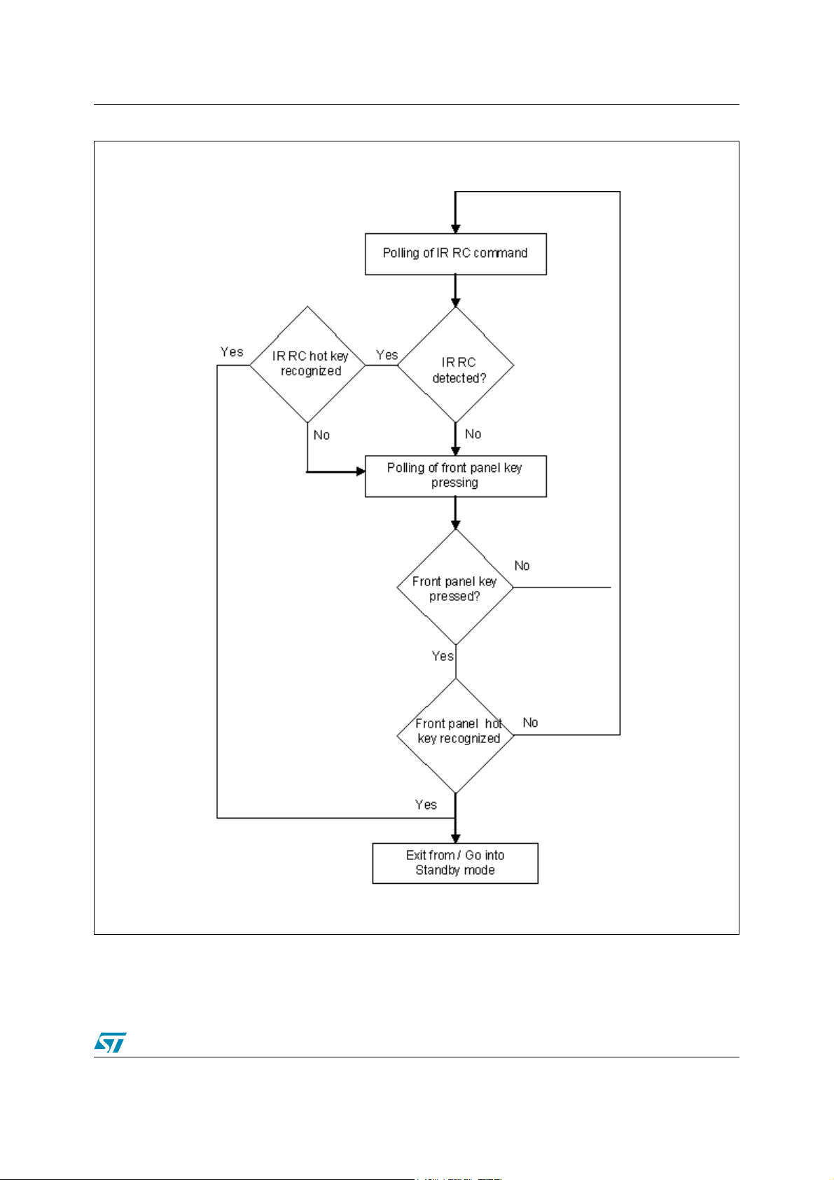
Figure 7. IR RC command and front panel key operation flowchart.
13/39

3 Initialization STFPC311
Figure 8. Watchdog timer first power-up operation
Figure 9. Watchdog timer operation
14/39
STFPC311 4 Display RAM address and display mode
4 Display RAM address and display mode
The display RAM stores the data transmitted from an external device to the STFPC311 through
the serial interface and is assigned addresses, in units of 8-bits see :Table 2.
Only the lower 4 bits of the addresses assigned to Seg
through Seg20 are valid, the higher 4
17
bits are ignored.
Note: The common grid/segment outputs are grid-based. The grid has to be enabled before any
segments can be turned on. If data is written for a segment before enabling its grid, there is
nothing on the display.
Table 2. Assigned addresses
Seg
1
00 H
03 H
06 H
09 H
0C H
0F H
12 H
15 H
18 H
1B H
1E H
21 H
24 H
27 H
2A H
2D H
b
0
XX H
Lower 4 bits Higher 4 bits
Seg
4
L
L
L
L
L
L
L
L
L
L
L
L
L
L
L
L
b3b
4
L
00 H
03 H
06 H
09 H
0C H
0F H
12 H
15 H
18 H
1B H
1E H
21 H
24 H
27 H
2A H
2D H
XX H
Seg
8
U
U
U
U
U
U
U
U
U
U
U
U
U
U
U
U
b
7
U
01 H
04 H
07 H
0A H
0D H
10 H
13 H
16 H
19 H
1C H
1F H
22 H
25 H
28 H
2B H
2E H
Seg
12
L
L
L
L
L
L
L
L
L
L
L
L
L
L
L
L
01 H
04 H
07 H
0A H
0D H
10 H
13 H
16 H
19 H
1C H
1F H
22 H
25 H
28 H
2B H
2E H
Seg
16
U
U
U
U
U
U
U
U
U
U
U
U
U
U
U
U
02 H
05 H
08 H
0B H
0E H
11 H
14 H
17 H
1A H
1D H
20 H
23 H
26 H
29 H
2C H
2F H
Seg
20
L
L
L
L
L
L
L
L
L
L
L
L
L
L
L
L
DIG
DIG
DIG
DIG
DIG
DIG
DIG
DIG
DIG
DIG
DIG
DIG
DIG
DIG
DIG
DIG
1
2
3
4
5
6
7
8
9
10
11
12
13
14
15
16
15/39

4 Display RAM address and display mode STFPC311
The data of each key is stored READ by a read command, starting from the least significant bit.
see Figure 11..
When the most significant bit of data (Seg
next data (Seg
) is read.
1b0
) has been read, the least significant bit of the
12b7
Figure 10. Key matrix (12 x 2 configuration) and key-input data storage RAM
Figure 11. Key storage and READ access
16/39

STFPC311 5 Data
5 Data
5.1 LED Port
Data is written to the LED port by a WRITE command, starting from the least significant bit of
the port see Figure 12. When a bit of this port is set to 0, the corresponding LED lights up;
when the bit is set to a 1, the LED turns off. The data of Bits 5 through 8 are ignored. Upon first
power-up, all of the LEDs are turned off.
Figure 12. LED port data WRITE command order
5.2 SW Data
The SW data are read by the appropriate READ command, starting from the least significant bit
see Figure 13. Bits 3 through 8 of the SW data are 0.
Figure 13. SW data READ Command order
17/39
6 Commands STFPC311
6 Commands
A command sets the display mode and status of the VFD driver. The first 1-byte input to the
STFPC311 through the D
set to high while commands/data are transmitted, the serial communication is initialized and the
commands/data being transmitted are invalid (however, the commands/data already
transmitted remain valid).
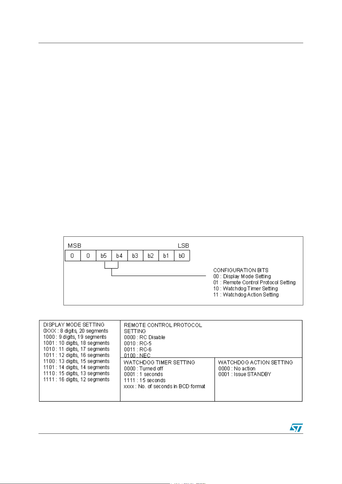
6.1 Configuration mode setting command
This command initializes the STFPC311 and performs any one of the following functions see
Figure 14.
a) Selects the number of segments and number of grids (1/8 to 1/16 duty, 12 segments
to 20 segments). When this command is executed, the display is turned off. To
resume display, the Display ON command must be executed. If the same mode is
selected, nothing is performed.
b) Selects the remote control protocol to use.
c) Sets the watchdog timer. The watchdog timer is configurable from 1s to 15s or turned
off completely.
d) Sets the watchdog action to perform when the watchdog timer counts. Two actions
are allowed: no action, and set STBY to (logic) high level.
pin after the STB pin goes low is regarded as a command. If STB is
IN
Figure 14. STFPC311 Configuration mode setting command order
Table 3. STFPC311 Configuration mode bit 3 through bit 0 settings
Note: Based on Bit 5 through Bit 4 settings.
18/39

STFPC311 6 Commands
Upon power application, the following modes are selected:
● Display Mode Setting: the 16-digit, 12-segment mode is selected (default: display off and
key-scan on).
● Remote Control Protocol Setting: RC-5.
● Watchdog Timer Setting: Turned on with 10s. After the first command is processed by
STFPC311, the watchdog timer is turned off until it is turned on by the host.
● Watchdog action: Issue Standby.
6.2 Data setting command
This command sets the data WRITE and READ modes see Figure 15.
Figure 15. STFPC311 Data setting command order
19/39

6 Commands STFPC311
When the application is powered-up, the normal operation mode and address increment mode
is set with the default display memory address set to 00H. In the auto-increment address mode,
the address command is sent once, followed by the data bytes.
Alternatively, the data command can be sent, followed by the data bytes. In this case, when new
display data is to be written, the last value of the address will be used and then incremented.
Upon reaching the last display memory address, the address jumps to 00H.
For fixed address mode, the address command has to be sent, followed by the display data.
When next byte of data is to be written, the address command has to be sent again before the
new display data byte.
For RC-5 data reception (after the photodiode), a binary 1 is represented by a high-to-low
transition, and a binary 0 is represented by a low-to-high transition. For RC-6 (Mode 0) data
reception, a binary 1 is represented by a low-to-high transition, and a binary 0 is represented by
a high-to-low transition. Whenever Bit 5 is a ‘1’, the watchdog timer is reset.
6.3 Address setting command
This command sets an address of the display memory. If address 30H or higher is set, the data
is ignored until a correct address is set.
Figure 16. STFPC311 Address Setting Command Order
6.4 Display control and hotkey setting command
When the application is powered-up, the 1/16-pulse width is set and the display is turned OFF.
See Figure 17 and Figure 4. All hot keys are disabled.
Figure 17. STFPC311 Display control and hot key setting command order
20/39

STFPC311 6 Commands
Table 4. STFPC311 Address setting mode bit 3 through bit 0 settings
21/39

7 Programmable hotkeys STFPC311
7 Programmable hotkeys
7.1 IR Remote control
Eight (8) commands are user programmable for hot key functions.
The address of the appliance (8-bit) is stored first into the internal RAM. Then, the command for
the hot keys are programmed into the internal RAM. Each hot key memory address could
accommodate one byte (8-bits). Usually one byte is reserved for one command. The RC data
is only cleared when the READY is pulled low (system goes into STANDBY state).
7.2 Front panel keys
Eight out of 24 keys are user programmable for hot key functions. Only keys from KS1 to KS4
can be programmed.
Figure 18. Programmable hot keys (only KS1 to KS4, Box FPK1)
8 hot keys are to be placed in each address location as indicated by the hotkey setting
command.
Figure 19. HOTKEY setting command address locations (8 hot keys)
For example, to store (Seg2/Key2) at the first location of the hot key RAM, the following
commands are sent:
● 10110000 (command+address), and
● 00010000 (hot key mask).
To store (Seg2/Key1), (Seg2/Key2), and (Seg4/Key1), the following commands are sent:
● 10110000 (command+address), and
● 00110010 (hot key mask).
The same commands apply to FPK2 and FPK3 programming.
Note: Note: Reading the hot key values immediately upon STBY de-assertion is recommended. If
they are not read within the watchdog preset timer value, the hot key data is cleared.
22/39

STFPC311 7 Programmable hotkeys
Figure 20. Recommended software flow
Note: Resetting the front panel controller at ¾ of the set watchdog time is recommended.
23/39

8 Default status STFPC311
8 Default status
8.1 Power-up default status
Table 5. Default States
S. N°
1Display OFF
2 Key-scan ON
3IR ON
4 Display mode 12 Seg/16Bit
5 Display address 00H
6 RC Protocol DC-5
7LED OFF
8 Dimming 1/16 Duty factor
9 Hot Kets (IR and FP) Disabled
10 Watchdog timer 10s
8.2 STANDBY status
The display remains ON during STANDBY only if the -20V is present. If the -20V is absent, the
display turns OFF. When the display wakes up from STANDBY and –20V is applied, the display
turns ON with previous value.
Switching off the display before entering the STANDBY state is recommended.
Functions Default Status
When the same display configuration command is sent, the display remains ON. When the
display configuration command is changed, the display is OFF.
Only hot key detection can wake the system up from STANDBY condition.
24/39

STFPC311 9 Remote control protocols
9 Remote control protocols
9.1 RC-5 remote control
RC-5 remote control protocol is based on Bi-phase (also known as Manchester) encoding as
shown in Figure 21.
Note: The encoding is set with reference to the IR_DATA_IN signal (after the photo diode). The MSB
is transmitted first see Figure 22.
● The first two Start bits (S1 and S2) are synchronization bits. For normal operation, they are
always set to '11' on the transmission side. After the photo diode, there is one inversion.
The data at the IR_DATA_IN of the STFPC311 is shown in Figure 23 on page 25
● The next bit is the Toggle bit. This bit is inverted each time a key on the remote control is
pressed.
● Bits A1and A5 are the Address bits. The address bits indicate the intended application that
the remote control protocol is used for.
● Bits C1..C6 are the Command bits. The command bits instruct the STFPC311 as to what
action is to be taken. The data representing the RC-5 protocol is sent as a byte of data
which consists of a Toggle bit and a ‘0’ bit followed by 6 bits of Command data.
Figure 21. Bi-phase encoding
Figure 22. RC-5 protocol frame
Figure 23. RC-5 reception example
25/39
9 Remote control protocols STFPC311
9.2 SPI interface IR data transmission
The IR data is sent on the DOUT pin of the SPI interface when the micro controller issues a IR
data read command. The data is sent in 3 bytes with LSB transmitted first as shown in the
Figure below:
The RC data consists of RC address, start bit, toggle bit and the RC command received. The
extra bits are stuffed with 1’s to make it a 3-byte packet. These extra bits at the end of the
packet should be ignored.
Figure 24. RC-6 protocol frame
The RC data consists of RC address, start bit, toggle bit and the RC command received. The
extra bits are stuffed with 1’s to make it a 3-byte packet. These extra bits at the end of the
packet should be ignored.
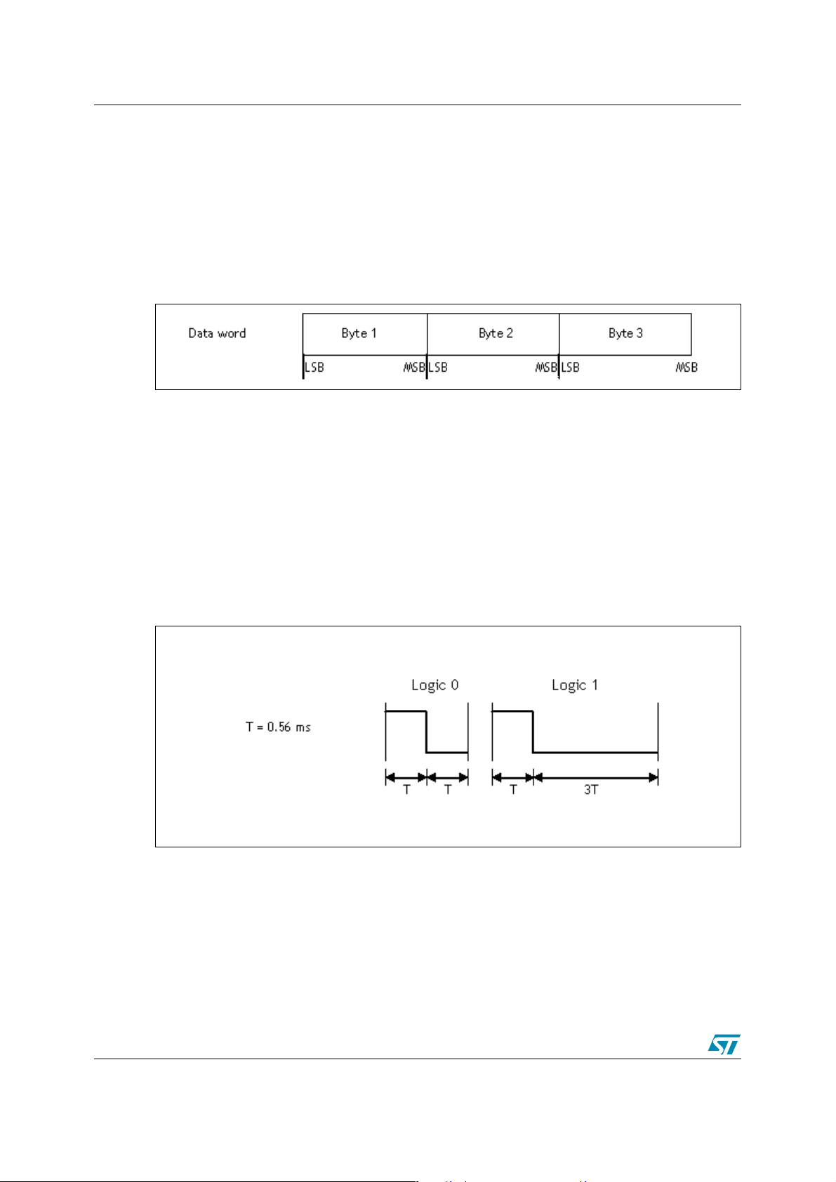
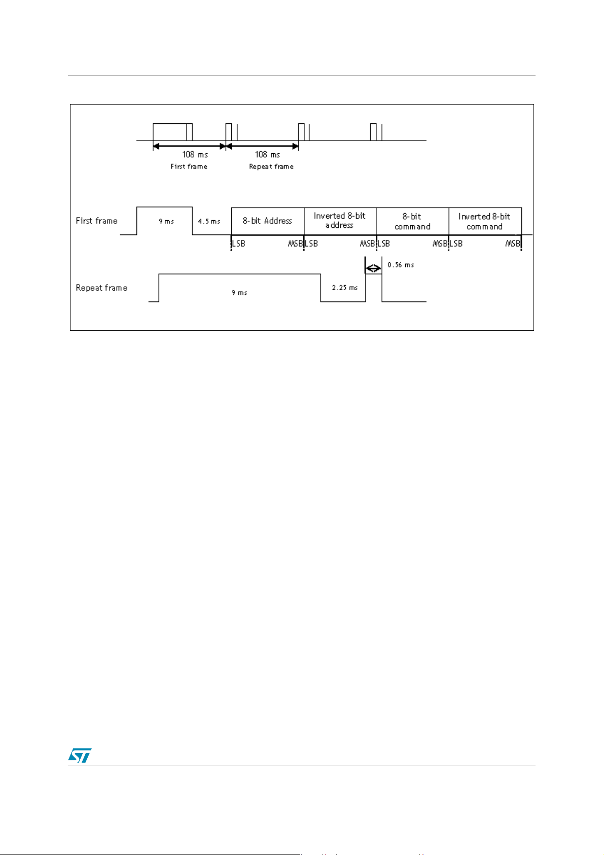
9.3 NEC remote control
This remote control protocol uses pulse distance modulation. Each bit consists of a high level of
fixed time "t", followed by a low level that varies in width. A space that is "t" represents a logic '0'
and a space that is "3t" represents a logic '1'. t = 0.56ms.
The LSB is transmitted first as shown in Figure 25
Figure 25. Pulse distance modulation.
26/39
STFPC311 9 Remote control protocols
Figure 26. NEC protocol transmission waveforms
27/39

10 Maximum rating STFPC311
10 Maximum rating
Stressing the device above the rating listed in the “Absolute Maximum Ratings” table may
cause permanent damage to the device. These are stress ratings only and operation of the
device at these or any other conditions above those indicated in the Operating sections of this
specification is not implied. Exposure to Absolute Maximum Rating conditions for extended
periods may affect device reliability. Refer also to the STMicroelectronics SURE Program and
other relevant quality documents.
Table 6. Absolute maximum rating ( T
= 25 °C, VSS = 0V )
A
Symbol Parameter Value Unit
V
DD
V
SS
V
V
O2
I
O1
I
O2
P
T
T
STG
1. Derate at -9.6 mW/°C at TA = 25 °C or higher
Logic Supply Voltage -0.5 to +7.0 V
+ 0.5 to V
Driver Supply Voltage
Logic Input Voltage
I1
VFP Driver Output Voltage
V
DD
-0.4 to V
V
SS
DD
– 0.5 to V
DD
+ 0.5
+ 0.5
DD
LED Driver Output Current +25 mA
VFP Driver Output Current
Power Dissipation
D
Operating Ambient Temperature -40 to +85 °C
A
-40 (grid)
-15 (segment)
(1)
1200
Storage Temperature -65 to +150 °C
– 40
Table 7. Recommended operating conditions (TA = -20 to +70 °C, VSS = 0V)
Symbol Parameter Min Typ Max Unit
V
DD
V
V
V
SS
Logic Supply Voltage 3.0 3.3 3.6 V
High-Level Input Voltage
IH
Low-Level Input Voltage 0
IL
0.7V
DD
Driver Supply Voltage 0
V
0.3 V
V
DD
DD
DD
-33.3
V
V
V
mA
mA
V
V
V
28/39

STFPC311 10 Maximum rating
10.1 Power consumption estimation
The maximum power consumption is comprised of the Vacuum Florescent Display (VFD) driver
dissipation, Load Resistance (RL), LED driver dissipation, and dynamic power consumption.
P
= VFD + RL + LED + P
MAX
Where,
● P
● VFD = Vacuum Florescent Display driver dissipation,
● R
● LED = LED driver dissipation, and
● PDYN = dynamic power consumption.
= maximum power consumption,
MAX
= load resistance,
L
If the segment current (ISEG) = 3mA, grid current (IGRID) = 15mA, and the LED current =
20mA, then:
FIP = (#segments x 6) + [#grids/(#grids +1)] x 30mW,
RL dissipation = (VDD – VSS)2 ÷ 50(segment + 1mW),
LED driver dissipation = #LEDs x 20mW, and
PDYN = VDD x 5mW.
To finish this example:
FIP driver dissipation = 16 x 6 + 12/13 x 30 = 124mW
RL dissipation = 33.32/50 x 17 = 377mW
LED driver dissipation = 2 x 20 = 40
PDYN = 3.3 x 5 = 16.5mW
DYN
The maximum power consumption (Total) = 557.5mW
Where,
VSS = –30V,
VDD = 3.3V, and the application is in 16-segment, 12-digit mode.
29/39
11 Electrical characteristics STFPC311
11 Electrical characteristics
Table 8. Electrical specifications
(T
= -20 to +70°C, VDD = 3.3V, VSS = 0V, V
A
Symbol Parameter Test conditions Min. Typ. Max. Unit
SS
= V
DD
- 33.3V)
V
V
V
I
OH21
I
OH22
I
OLEAK
High-Level Output Voltage
OH1
Low-Level Output Voltage
OL1
Low-Level Output Voltage
OL2
High-Level Output Current
High-Level Output Current
Driver Leakage Current
R
Output Pull-Down Resistor Driver output 50 100 150 kΩ
L
I Input Current
V
High-Level Input Voltage
IH
V
Low-Level Input Voltage
IL
V
Hysteresis Voltage
H
I
DD(DYN)
Dynamic Current
Consumption
LED1 – LED4, I
LED1 – LED4, I
, I
D
V
V
Se
V
OUT
O
O
13
O
= 4mA
OL2
= V
– 2V, Seg
DD
= V
– 2 V, Grid
DD
g/Grid16to Seg20/Grid
= V
– 33.3 V, driver off
DD
VI= VDD or V
CLK, D
, STB
IN
Under no load, display off 5 mA
Table 9. Switching characteristics (TA = -20 to +70 °C, V
= -1mA 0.9V
OH1
= 20mA
OH2
to Seg
1
to Grid8,
1
SS
12
9
DD
-3 mA
-15 mA
0.7V
DD
0.35 V
= 3.3 V, V
DD
= -30 V)
SS
1V
0.4 V
-10 µA
±1 µA
0.3V
DD
Symbol Parameter Test conditions Min. Typ. Max. Unit
V
V
V
t
t
t
t
TZH1
t
TZH2
t
f
Oscillation Frequency R = 33KΩ ±5% 350 500 650 kHz
OSC
PLZ
Propagation Delay Time
PZL
Rise Time
Fall Time
THZ
Maximum Clock
MAX
Frequency
C
Input Capacitance 15 pF
I
CLK ≤ D
CL = 15pF, RL = 10KΩ
C
= 300pF
L
C
= 300pF, Segn, Grid
L
Duty = 50% 1 MHz
30/39
OUT
Seg
to Seg
1
12
Grid1 to Grid8,
/Seg16 to
Seg
13
/Grid
Seg
20
9
n
300 ns
100 ns
2 µs
0.5 µs
120 µs
STFPC311 12 Timing characteristics
12 Timing characteristics
Table 10. Timing characteristics ( VDD= 3.3V, TA= -20 to 70°C, unless otherwise noted.
Typical values are at T
Symbol Parameter Test conditions
= 25°C )
A
Values
Unit
Min. Typ. Max.
PW
PW
t
SETUP
t
HOLD
t
CLK-STB
t
WAIT
1. Refer to page on Serial Communication Format.
Clock Pulse Width 400 ns
CLK
Strobe Pulse Width 1 µs
STB
Data Setup Time 100 ns
Data Hold Time 100 ns
Clock-Strobe Time CLK STB 1 µs
Wait Time
(1)
CLK CLK 1 µs
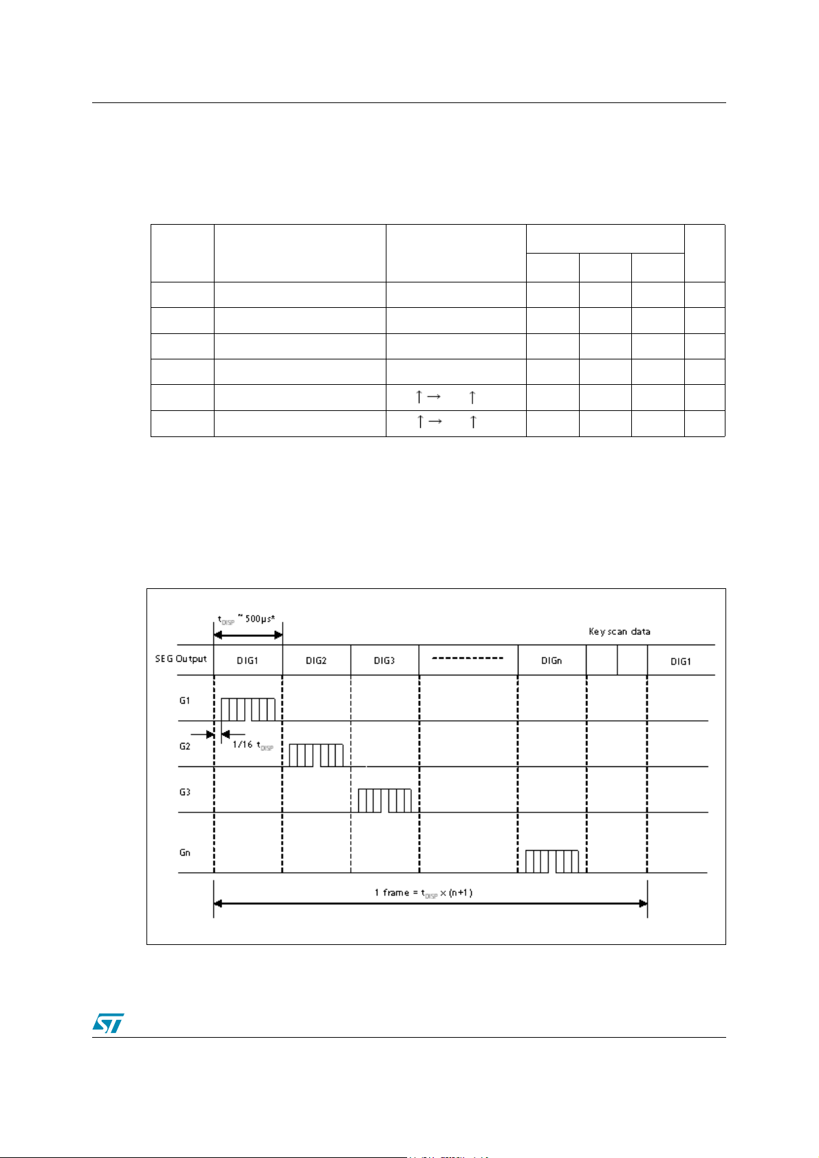
The pulse width of the segment signal is derived from the oscillator frequency. The value can be
modified by trimming ROSC. One cycle of key scanning consists of one frame and data of 12 x
2 matrices are stored in RAM.
Note: The key scan is only at the end of the frame when the display is ON. When the display is OFF,
the key scan takes place continuously. The grid is turned off during the key scan.
Figure 27. Key scanning and display timing
31/39

13 Serial communication format STFPC311
13 Serial communication format
When data is read, a wait time (t
clock that has set the command, and the falling edge of the first clock that has read the data.
This is required by the STFPC311 to process its internal commands/data (See Figure 28)
Caution: Care must be taken to connect an external pull-up resistor to this pin (1kΩ to 10kΩ) because the
D
pin is an N-channel, open drain output pin (see Figure 29).
OUT
Figure 28. Recption (Command/data WRITE)
) of 1µs is necessary within the rising edge of the eighth
WAIT
Figure 29. Data transmission (data READ)
32/39

STFPC311 13 Serial communication format
Figure 30. Switching characteristic waveforms
f
f
OSC
OSC
OSC
OSC
50%
50%
PW
PW
STB
STB
STB
STB
CLK
CLK
D
D
IN
IN
D
D
OUT
OUT
Sn/G
Sn/G
PW
PW
CLK
CLK
t
t
SETUP
SETUP
90%
90%
n
n
10%
10%
PW
PW
t
t
HOLD
HOLD
CLK
CLK
t
t
THZ
THZ
t
t
CLK-STB
CLK-STB
t
t
PZL
PZL
t
t
TZH
TZH
t
t
PLZ
PLZ
33/39

13 Serial communication format STFPC311
● Command 1: sets display mode
● Command 2: sets data
● Command 3: sets address
● Data 1 to n: transfers display data (22 bytes max.)
● Command 4: controls display
Figure 31. Updating display memory by incrementing address
● Command 1: sets data
● Command 2: sets address
● Data: display area
Figure 32. Updating specific address
34/39

STFPC311 14 Typical application diagram
14 Typical application diagram
Figure 33. Typical application circuit
R5
R5
R6
+
+
C1
C1
R6
D1
D1
V
V
DD
DD
C2
C2
1
1
<
<
2
2
<
<
3
3
<
<
4
4
<
<
5
5
<
<
6
6
<
<
7
7
<
<
8
8
<
<
9
9
<
<
10
10
VDD3.3V±0.3V
11
11
12
12
VDD3.3V±0.3V
VSS* -30V
VSS* -30V
GND
GND
GND
GND
<
<
<
<
<
<
R
R
OSC
OSC
KEY1 KEY2
KEY1 KEY2
V
V
DD
DD
OSC
OSC
STB
STB
CLK
CLK
D
D
IN
IN
D
D
OUT
OUT
IR_DATA_IN
IR_DATA_IN
READY/STBY_n
READY/STBY_n
NC
NC
MUTE
MUTE
STBY
STBY
SEG1/K1
SEG1/K1
STFPC311
STFPC311
12 x 2
12 x 2
KEYBOARD
KEYBOARD
V
V
SS
SS
D12
D12
SEG12/K12
SEG12/K12
S13/G16 ~ S20/G9
S13/G16 ~ S20/G9
G1 ~ G8
G1 ~ G8
LED1
LED1
LED2
LED2
LED3
LED3
LED4
LED4
V
V
SS
SS
C3 C4
C3 C4
+
+
8 Grids/Segments
8 Grids/Segments
8 Grids
8 Grids
R1
R1
R2
R2
R3
R3
R4
R4
V
V
DD
DD
VFD
VFD
Ef
Ef
● R
= 33kΩ ± 1% for oscillator resistor;
OSC
● R1 ~ R4 = 0.75 ~ 1.2kΩ;
● R5, R6 = 10kΩ for external keyboard pull-down resistor;
● C1 = 33µF-25V electrolytic;
● C2 = 0.01 ~ 0.1µF-25V ceramic;
● C3 = 0.01 ~ 0.1µF-63V ceramic;
● C4 = 33µF-63V electrolytic;
● D1 ~ D12 = 1N4148;
● Ef = filament voltage according with the VFD specs;
● V
* V
= 3.3V ±10%;
DD
= down to VDD – 33.3V.
SS
35/39

15 Package mechanical data STFPC311
15 Package mechanical data
In order to meet environmental requirements, ST offers these devices in ECOPACK® packages.
These packages have a Lead-free second level interconnect. The category of second Level
Interconnect is marked on the package and on the inner box label, in compliance with JEDEC
Standard JESD97. The maximum ratings related to soldering conditions are also marked on
the inner box label. ECOPACK is an ST trademark. ECOPACK specifications are available at:
www.st.com.
36/39

STFPC311 15 Package mechanical data
Table 11. PQFP52 - 10x10x2 mm. plastic quad flatpack, package mechanical data
Figure 34. Package dimensions
37/39

16 Revision history STFPC311
16 Revision history
Table 12. Revision history
Date Revision Change
09-May-2006 1 First release
38/39

STFPC311 16 Revision history
Please Read Carefully:
Information in this document is provided solely in connection with ST products. STMicroelectronics NV and its subsidiaries (“ST”) reserve the
right to make changes, corrections, modifications or improvements, to this document, and the products and services described herein at any
time, without notice.
All ST products are sold pursuant to ST’s terms and conditions of sale.
Purchasers are solely responsible for the choice, selection and use of the ST products and services described herein, and ST assumes no
liability whatsoever relating to the choice, selection or use of the ST products and services described herein.
No license, express or implied, by estoppel or otherwise, to any intellectual property rights is granted under this document. If any part of this
document refers to any third party products or services it shall not be deemed a license grant by ST for the use of such third party products
or services, or any intellectual property contained therein or considered as a warranty covering the use in any manner whatsoever of such
third party products or services or any intellectual property contained therein.
UNLESS OTHERWISE SET FORTH IN ST’S TERMS AND CONDITIONS OF SALE ST DISCLAIMS ANY EXPRESS OR IMPLIED
WARRANTY WITH RESPECT TO THE USE AND/OR SALE OF ST PRODUCTS INCLUDING WITHOUT LIMITATION IMPLIED
WARRANTIES OF MERCHANTABILITY, FITNESS FOR A PARTICULAR PURPOSE (AND THEIR EQUIVALENTS UNDER THE LAWS
OF ANY JURISDICTION), OR INFRINGEMENT OF ANY PATENT, COPYRIGHT OR OTHER INTELLECTUAL PROPERTY RIGHT.
UNLESS EXPRESSLY APPROVED IN WRITING BY AN AUTHORIZE REPRESENTATIVE OF ST, ST PRODUCTS ARE NOT DESIGNED,
AUTHORIZED OR WARRANTED FOR USE IN MILITARY, AIR CRAFT, SPACE, LIFE SAVING, OR LIFE SUSTAINING APPLICATIONS,
NOR IN PRODUCTS OR SYSTEMS, WHERE FAILURE OR MALFUNCTION MAY RESULT IN PERSONAL INJURY, DEATH, OR
SEVERE PROPERTY OR ENVIRONMENTAL DAMAGE.
Resale of ST products with provisions different from the statements and/or technical features set forth in this document shall immediately void
any warranty granted by ST for the ST product or service described herein and shall not create or extend in any manner whatsoever, any
liability of ST.
ST and the ST logo are trademarks or registered trademarks of ST in various countries.
Information in this document supersedes and replaces all information previously supplied.
The ST logo is a registered trademark of STMicroelectronics. All other names are the property of their respective owners.
© 2006 STMicroelectronics - All rights reserved
STMicroelectronics group of companies
Australia - Belgium - Brazil - Canada - China - Czech Republic - Finland - France - Germany - Hong Kong - India - Israel - Italy - Japan -
Malaysia - Malta - Morocco - Singapore - Spain - Sweden - Switzerland - United Kingdom - United States of America
www.st.com
39/39
 Loading...