

Page 1
XR-C440/C450
SERVICE MANUAL
Ver 1.1 2001.08
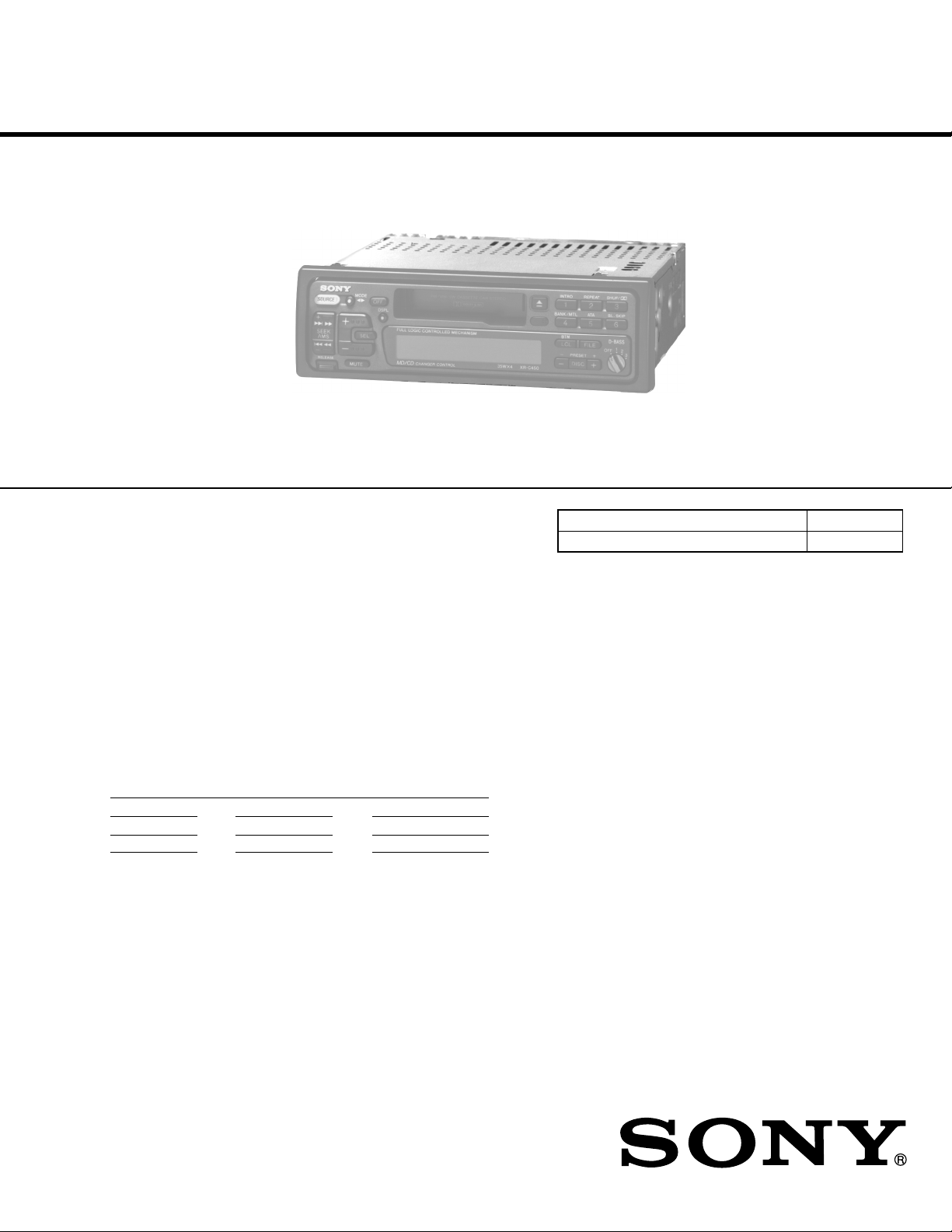
Photo: XR-C450
Refer to RM-X2S/X3S SERVICE MANUAL (9-960-039-∏)
issued previously for information of remote commander
(RM-X2S) supplied with XR-C440.
US Model
Canadian Model
XR-C450
E Model
XR-C440/C450
Dolby noise reduction manufactured under license
from Dolby Laboratories Licensing Corporation.
“DOLBY” and the double-D symbol a are trademarks
of Dolby Laboratories Licensing Corporation.
SPECIFICATIONS
AUDIO POWER SPECIFICATIONS (US model)
POWER OUTPUT AND TOTAL HARMONIC DISTORTION
12 watts per channel minimum continuous average power into 4 ohms, 4 channels driven from 20 Hz to 20 kHz with no more than 1% total
harmonic distortion.
Cassette player section
Tape track 4-track 2-channel stereo
Wow and flutter 0.08% (WRMS)
Frequency response 30 – 18,000 Hz (C440/C450: US, Canadian)
30 – 20,000 Hz (C450: E, Saudi Arabia)
Signal-to-noise ratio
Cassette type Dolby B NR Dolby NR off
TYPE II, IV 67 dB 61 dB
TYPE I 64 dB 58 dB
Tuner section
FM
Tuning range US, Canadian model:
87.5 – 107.9 MHz
E, Saudi Arabia model:
50 kHz/200 kHz switchable
87.5 – 108.0 MHz (at 50 kHz step)
87.5 – 107.9 MHz (at 200 kHz step)
Model Name Using Similar Mechanism NEW
T ape Transport Mechanism T ype
Antenna terminal External antenna connector
Intermediate frequency 10.7 MHz
Usable sensitivity 8 dBf
Selectivity 75 dB at 400 kHz
Signal-to-noise ratio 65 dB (stereo),
68 dB (mono)
Harmonic distortion at 1 kHz
0.5% (stereo),
0.3% (mono)
Separation 35 dB at 1 kHz
Frequency response 30 – 15,000 Hz
Capture ratio 2 dB (C450: E, Saudi Arabia)
4 dB (C440/C450: US, Canadian)
— Continued on next page —
MG-25C-136
XR-C440/C450: US, Canadian Model
FM/AM CASSETTE CAR STEREO
FM/MW/SW CASSETTE CAR STEREO
9-925-536-12 Sony Corporation
2001H0500-1 e Vehicle Company
C 2001.8 Shinagawa Tec Service Manual Production Group
XR-C450: E Model
Page 2

AM (MW)
Tuning range US, Canadian model:
530 – 1,710 MHz
E, Saudi Arabia model:
9 kHz/10 kHz switchable
531 – 1,602 kHz
(at 9 kHz step)
530 – 1,710 kHz
(at 10 kHz step)
SW (C450: E, Saudi Arabia)
Tuning range SW tuning interval:
SW1: 2,940 – 7,735 kHz
SW2: 9,500 – 18,135 kHz
(except for 10,140 – 11,575 kHz)
Antenna terminal External antenna connector
Intermediate frequency 10.71 MHz/450 kHz
Sensitivity 30 µV (C440/C450: US, Canadian)
40 µV (C450: E, Saudi Arabia)
TABLE OF CONTENTS
1. GENERAL
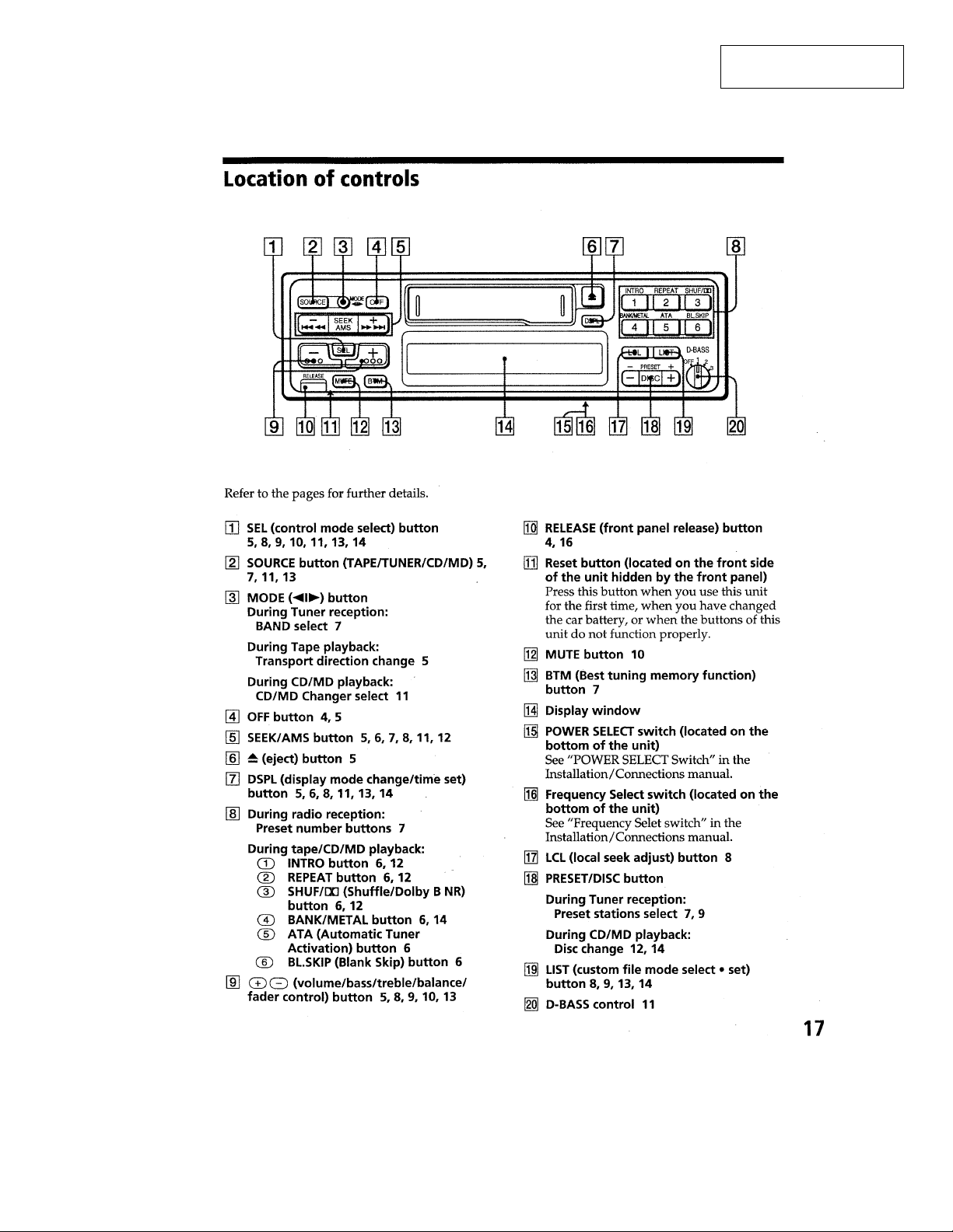
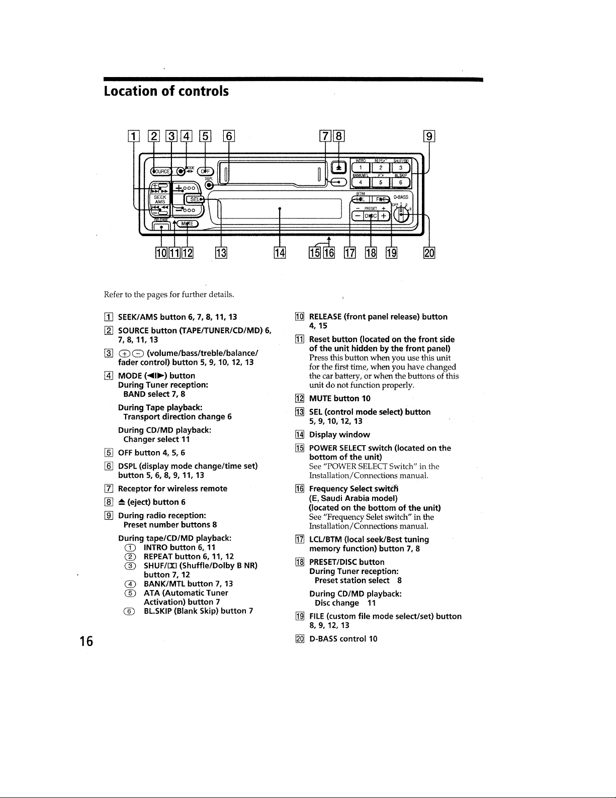
Location of Controls (XR-C440)....................................... 3
Location of Controls (XR-C450)....................................... 4
Installation (XR-C440/XR-C450: E, saudi Arabia)........... 6
Installation (XR-C450: US, Canadian).............................. 7
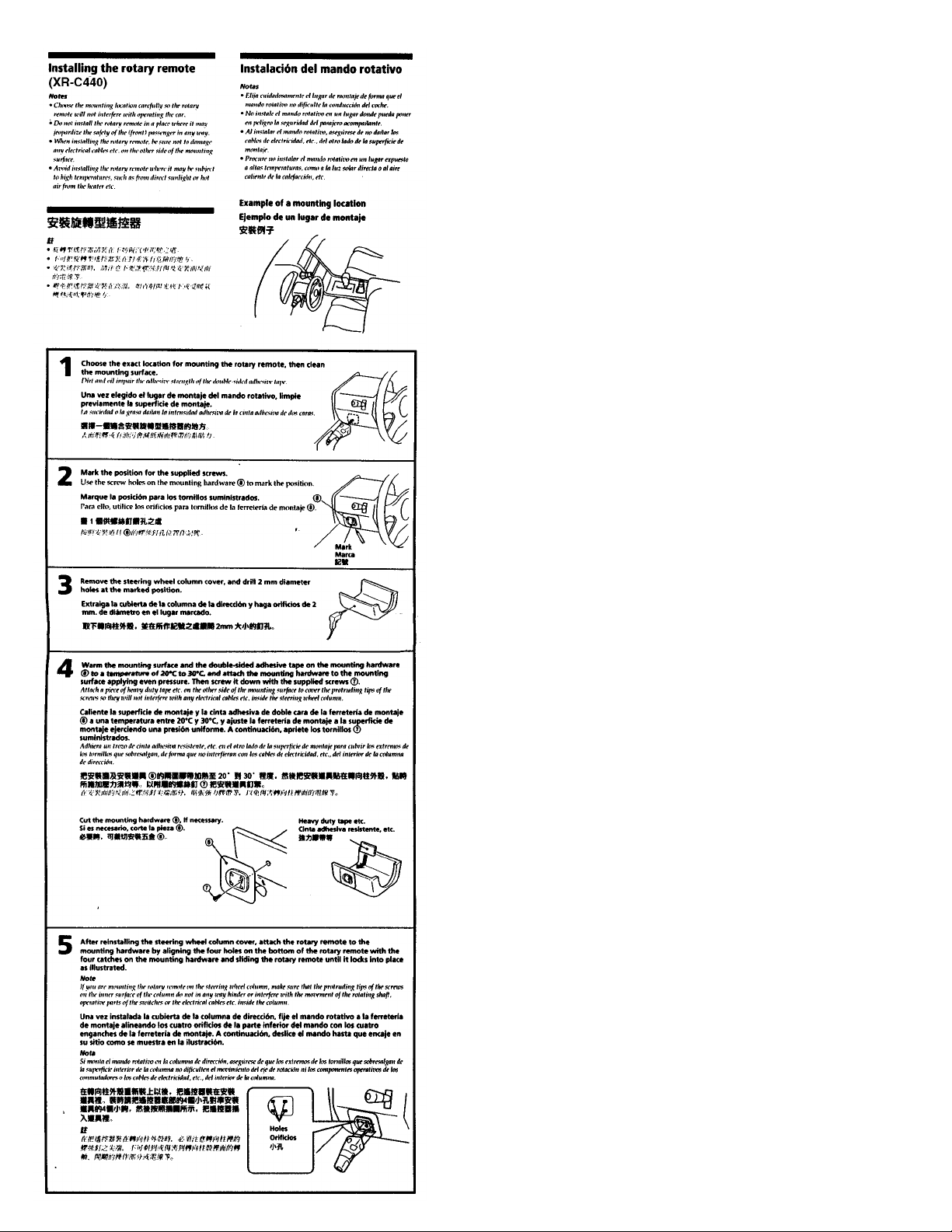
Installing the rotary remote (XR-C440) ............................ 8
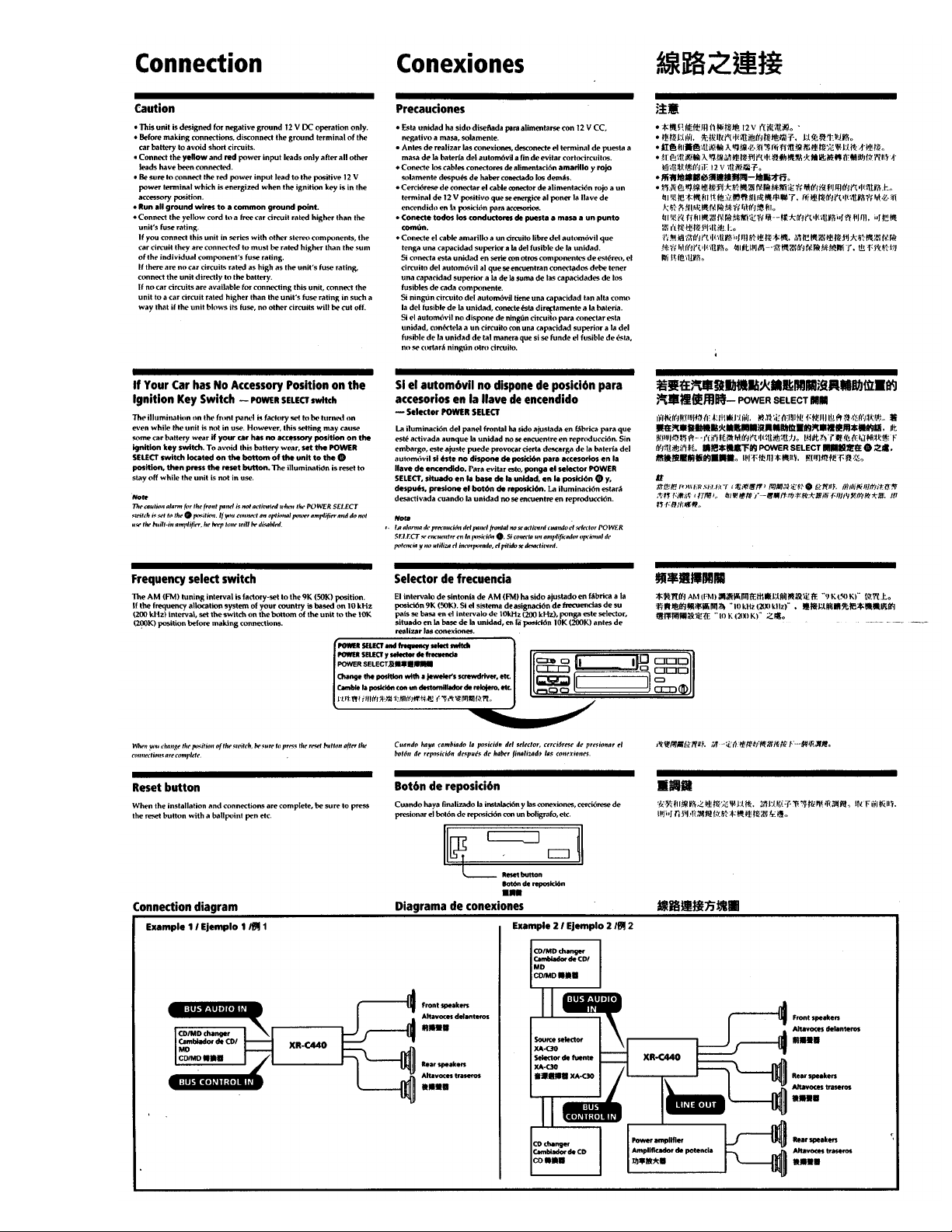
Connection (XR-C440) ..................................................... 9
Connection (XR-C450) ..................................................... 11
2. DISASSEMBLY............................................................ 14
3. ASSEMBLY OF MECHANISM DECK ............. 16
4. MECHANICAL ADJUSTMENTS ......................... 19
Power amplifier section
Outputs Speaker outputs
Speaker impedance 4 – 8 ohms
Maximum power output 35 W × 4 (at 4 ohms)
General
Outputs Power antenna control lead
Tone controls Bass ±8 dB at 100 Hz
Power requirements 12 V DC car battery
Dimensions Approx. 188 × 58 × 181 mmm
Mounting dimensions Approx. 182 × 53 × 164 mmm
Mass Approx. 1.2 kg (2 lb. 10 oz.)
Supplied accessories Parts for installation and connections (1 set)
Design and specifications are subject to change without notice.
(sure seal connectors)
Line out
Rear (1)
Front (1) (C450)
Treble ±8 dB at 100 Hz
(negative ground)
1
(7
/2 × 2 3/8 × 7 1/4 in.)
(w / h / d)
(7 1/4 × 2 1/8 × 6 1/2 in.)
(w / h / d)
Front panel case (1)
Rotary remote
RM-X2S (C440)
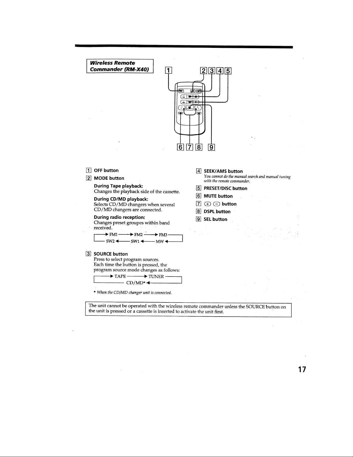
Wireless Remote
Commander RM-X40 (C450: E, Saudi Arabia)
5. ELECTRICAL ADJUSTMENTS
Test Mode .......................................................................... 19
Tape Deck Section ............................................................. 20
Tuner Section (XR-C450: E, Saudi Arabia) ...................... 20
6. DIAGRAMS
6-1. Printed Wiring Board –Main Section– .............................. 23
6-2. Schematic Diagram –Main Section–................................ 25
6-3. Printed Wiring Board –Key Section– (XR-C440) ............ 29
6-4. Schematic Diagram –Key Section– (XR-C440) ............... 31
6-5. Printed Wiring Board –Key Section– (XR-C450) ............ 33
6-6. Schematic Diagram –Key Section– (XR-C450) ............... 35
6-7. IC Pin Function Description.............................................. 39
7. EXPLODED VIEWS .................................................. 41
8. ELECTRICAL PARTS LIST.................................. 45
Flexible Circuit Board Repairing
• Keep the temperature of the soldering iron around 270 ˚C during
repairing.
• Do not touch the soldering iron on the same conductor of the
circuit board (within 3 times).
• Be careful not to apply force on the conductor when soldering or
unsoldering .
Notes on chip component replacement
• Never reuse a disconnected chip component.
• Notice that the minus side of a tantalum capacitor may be dam-
aged by heat.
– 2 –
Page 3
SECTION 1
GENERAL
(XR-C440)
This section is extracted
from instruction manual.
– 3 –
Page 4
(XR-C450)
– 4 –
Page 5
(XR-C450: E, Saudi Arabia)
– 5 –
Page 6
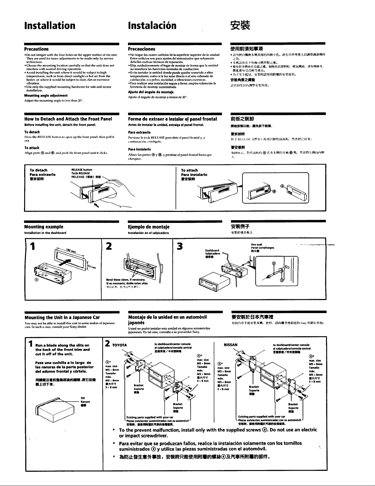
(XR-C440/XR-C450: E, Saudi Arabia)
– 6 –
Page 7
(XR-C450: US, Canadian)
– 7 –
Page 8
– 8 –
Page 9
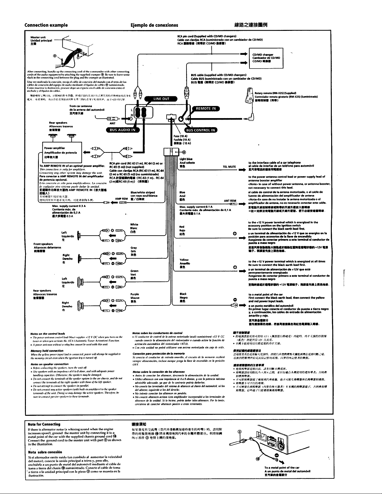
(XR-C440)
– 9 –
Page 10
– 10 –
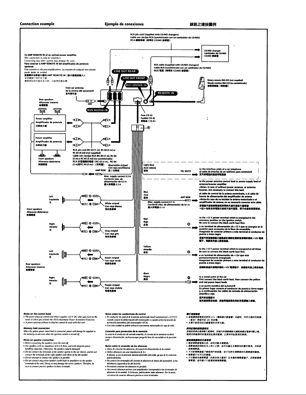
Page 11

(XR-C450)
(E, Saudi Arabia model)
– 11 –
Page 12
(E, Saudi Arabia model)
– 12 –
Page 13
(US, Canadian model)
(E, Saudi Arabia model)
– 13 –
Page 14

SECTION 2
DISASSEMBLY
Note: Follow the disassembly procedure in the numerical order given.
FRONT PANEL ASS’Y
1
Push the button
(release).
A
2
Remove the front panel ass’y
to the direction of the arrow A.
COVER ASS’Y
1
2
3
cover ass’y
2
1
– 14 –
Page 15

SUB PANEL, MECHANISM DECK
3
connector
(CN302)
2
sub panel
1
three screws
(PTT2.6 × 8)
5
screw
(PTT2.6 × 6)
6
mechanism deck
4
flexible flat cable
(CN301)
1
three screws
(PTT2.6 × 8)
MAIN BOARD, HEAT SINK
2
two ground point
screws
3
main board
1
two screws
(PTT2.6 × 8)
1
5
heat sink
4
nine screws
(PTT2.6 × 10)
screw
(PTT2.6 × 8)
– 15 –
Page 16

SECTION 3
ASSEMBLY OF MECHANISM DECK
Note: Follow the assembly procedure in the numerical order given.
HOUSING
4
Fit claw on B part.
3
2
Install the hanger onto
two claws of the housing.
Put the housing
under
A
part.
housing
A
part
5
Fit projection on C part.
C
part
7
Holder the hanger by bending the claw.
1
Install the catch to the hanger.
hanger
6
Fit projection on D part.
8
Hold the hanger by
bending the claw.
D
part
ARM (SUCTION)
B
projection
part
2
Move the arm (suction) in the arrow
direction and fit on projection.
1
Fit the arm (suction) on the shaft.
– 16 –
Page 17

LEVER (LDG-A) / (LDG-B)
shaft
A
shaft
1
Fit the lever (LDG-A) on
shafts A – C and install it.
B
shaft
C
4
type-E stop ring 2.0
shaft
A
shaft
2
3
Fit the lever (LDG-B) on
shafts A and B and
install it.
B
Pull the lever in the
arrow direction.
GEAR (LDG-FT)
hole
hole
gear (LDG-D)
lever (LDG-A)
gear (LDG-FB)
5
gear (LDG-FT)
5
polyethyene washer
1
2
Move the lever (LDG-B)
in the arrow direction.
tension spring (lever LDG)
3
Align hole in the gear (LDG-D)
with hole the lever (LDG-A).
– 17 –
Page 18

GUIDE (C)
1
three claws
2
guide (C)
– 18 –
Page 19

SECTION 4
MECHANICAL ADJUSTMENTS
1. Clean the following parts with a denatured-alcohol-moistened
swab:
playback head pinch roller
rubber belt capstan
idles
2. Demagnetize the playback head with a head demagnetizer.
3. Do not use a magnetized screwdriver for the adjustments.
4. After the adjustments, apply suitable locking compound to the
parts adjusted.
5. The adjustments should be performed with the power supply
voltage unless otherwise noted.
SECTION 5
ELECTRICAL ADJUSTMENTS
TEST MODE
This set have the test mode function. In the test mode, FM Auto
Scan/Stop Level and AM (MW) Auto Scan/Stop Level adjustments
can be performed easier than it in ordinary procedure.
<Set the Test Mode>
1. Set the “OFF” mode.
2. Push the preset 4 button.
3. Push the preset 5 button.
4. Press the preset 1 button for more than two seconds.
5. Then the display indicates all lights, the test mode is set.
• T orque Measurement
Mode Torqu Meter Meter Reading
Forward CQ-102C
Forward
Back Tension (0.01 - 0.06 oz·inch)
Reverse CQ-102RC
Reverse
Back Tension (0.01 - 0.06 oz·inch)
FF, REW CQ-201B
• T ape Tension Measurement
Mode Torqu Meter Meter Reading
Forward CQ-403A
Reverse CQ-403R
CQ-102C
CA-102RC
30 - 65 g·cm
(0.42 - 0.90 oz·inch)
0.5 - 4.5g·cm
30 - 65 g·cm
(0.42 - 0.90 oz·inch)
0.5 - 4.5g·cm
60 - 200 g·cm
(0.83 - 2.78 oz·inch)
more than 90 g
(more than 3.18 oz)
more than 90 g
(more than 3.18 oz)
<Release the Test mode>
1. Push the “OFF” button.
– 19 –
Page 20

See the adjustment location from on page 22 for the ad-
r
justment.
TUNER SECTION
(XR-C450: E, Saudi Arabia model only)
0 dB=0.775 VTAPE DECK SECTION
Tape Speed Adjustment
Procedure:
1. Put the set into the FWD PB mode.
test tape
WS-48A
(3 kHz, 0 dB)
set
LINE OUT
frequency counte
10 kΩ
Specification: Constant speed
Speed checker Frequency counter
–1.5 to +2.5% 2,955 to 3,075Hz
Adjustment Location: See page 22.
DOLBY Level Adjustment
Setting:
Preset 3 (DOLBY) button : OFF
SEL (BAS) button : Center
SEL (TRE) button : Center
SEL (BAL) button : Center
SEL (FAD) button : Center
SEL (VOL) button : Maximum
D-BASS control : OFF
speed checker
or
+–
0dB=1µV
Cautions during repair
When the tuner unit is defective, replace it by a new one because
its internal block is difficult to repair.
FM Auto Scan/Stop Level Adjustment
Setting:
SOURCE button : FM
FREQUENCY SELECT switch: 10 k
FM RF signal
generator
Carrier frequency : 97.9 MHz
Output level : 22 dB (12.6 µV)
Mode : mono
Modulation : 1 kHz, 75 kHz deviation
antenna jack (J1)
0.01 µF
set
Procedure:
1. Set to the test mode. (See page 19).
2. Push the SOURCE button and set to FM.
Display
FM
SHUF1
3. Push the preset 3 button.
test tape
P-4-D400
(400Hz, 0dB)
main board
TP (DOLBY )
set
L-CH: IC301 7
R-CH: IC301@¢
main board
TP (GND)
level meter
+
–
Procedure:
1. Put the set into the FWD PB mode.
2. Adjust R V231 (L-CH) and R V131 (R-CH) so that the lev el meter
reading is –6±0.5 dB (0.37 to 0.41 V).
Adjustment Location: See page 22.
Display
FM
SHUF1
4. Adjust with the volume RV2 on TU1 so that the “FM” indication turns to “FM0” indication on the display window.
But, in case of already indicated “FM0”, turn the RV2 so that
put out light “0” indication and adjustment.
Display
SHUF1
Adjustment Location: See page 22.
– 20 –
Page 21

FM Noise Focus Adjustment
(
)
r
r
1
SHUF1
3
Setting:
SOURCE button : FM
FREQUENCY SELECT switch: 10 k
FM RF signal
generator
Carrier frequency : 97.9 MHz
Output level : 60 dB (1 mV)
Mode : mono
Modulation : 1 kHz, 75 kHz deviation
Procedure :
1. Tune the 97.9 MHz
2. The then output level is supposing that (A) dB.
3. Adjust with the volume RV3 on TU1 so that the output level is
(A) –32 dB then signal generator input set to –20 dB.
Adjustment Location: See page 22.
FM Stereo Separation Adjustment
Setting:
SOURCE button : FM
FREQUENCY SELECT switch: 10 k
FM RF signal
generator
Carrier frequency : 97.9 MHz
Output level : 70 dB (3.2 mV)
Mode : stereo
Modulation :
FM Stereo
signal generator
output channel
L-CH L-CH A
R-CH L-CH Adjust RV4 on TU1
R-CH R-CH C
L-CH R-CH Adjust RV4 on TU1
Procedure:
L-CH Stereo separation: A-B
R-CH Stereo separation: C-D
The separations of both channels should be equal.
antenna jack (J1)
0.01 µF
set
antenna jack (J1)
0.01 µF
set
main: 1 kHz, 20 kHz deviation (26%)
sub: 1 kHz, 20 kHz deviation (26%)
19 kHz pilot: 7.5 kHz deviation (10%)
Level meter Level meter
connection reading (dB)
10 k Ω
LINE OUT
10 k Ω
LINE OUT
for minimum reading.
for minimum reading.
level mete
+
–
level mete
+
–
B
D
AM (MW) Auto Scan/Stop Level Adjustment
Setting:
SOURCE and MODE button : MW
FREQUENCY SELECT switch: 10 k
30 Ω
15 pF
65 pF
AM RF signal
generator
AM dummy antenna
(50 Ω)
Carrier frequency : 1000 kHz
30% amplitude
modulation by
400 Hz signal
Output level : 33 dB
Procedure:
1. Set to the test mode. (See page 19.)
2. Push the SOURCE button and set to FM.
3. Push the MODE button and set to MW.
44.7 µV
Display
set
antenna jack (J1)
MW
1
4. Push the preset 3 button.
Display
SHUF1
MW
3
5. Adjust with the volume RV1 on TU1 so that the “MW” indication turns to “MW0” indication on the display window.
But, in case of already indicated “MW0”, turn the RV1 so that
put out light “0” indication and adjustment.
Adjustment Location: See page 22.
1
Display
SHUF1
Specification: Separation more than 30 dB
Adjustment Location: See page 22.
– 21 –
Page 22

Adjustment Location:
Tape Speed Adjustment
– SET UPPER VIEW –
(XR-C450: E, Saudi Arabia model only)
TU1
RV1 AM (MW) Auto Scan/Stop Level Adjustment
RV2 FM Auto Scan/Stop Level Adjustment
RV3 FM Noise Focus Adjustment
RV4 FM Stereo Separation Adjustment
RV131
(R-CH)
– MAIN BOARD (CONDUCTOR SIDE) –
RV231
(L-CH)
DOLBY Level
Adjustment
TU1
J1
antenna jack
TP (DOLBY R)
TP (GND)
IC301
TP (DOLBY L)
IC501
– 22 –
Page 23

Page 24

Page 25

Page 26

Page 27

• IC Block Diagrams
IC1 BU2624F-E2
1
XOUT
2
XIN
3
CE
4
CK
5
DA
6
CD
7
P0
8
P1
9
P3
10
P4
CONTROL
REFERENCE
DIVIDER
I/O
20BIT COUNT
SHIFT
REGISTER
LATCH
MAIN
COUNT
IF COUNT
CONTROL
PHASE
DETECT
PRESCALLER
IC361 MM1322XFBE
20
VSS
19
PD1
18
VDD
17
FMIN
16
AMIN
GND
IN2
VCC
IN1
1
2
3
CONTROL CIRCUIT
4
8
OUT2
7
VS
6
OUT1
5
GND
IC651 RN5VD23AA-TL
15
P2
14
IF1
13
IF2
CD
5
NC
4
VREF
+
–
IC161 LC75373ED
LVRIN
+
–
34
LSELO
35
L4
L3
36
L2
VDD
RSELO
37
L1
38
39
R1
40
41
R2
R3
42
R4
43
44
+
–
–
+
–
+
LCOM
12
SD
11
PD2
LS3
LS1
LSIN
LT3
LT2
LT1
+
–
+
–
+
–
–
+
LTOUT
2627282930313233
–
+
DECODER LATCH
+
–
LS2
25
–
+
–
+
REGISTER
+
–
+
–
SHIFT
1
OUT
LSOUT
2324
CONTROL
2 3
VDD
22
LFIN
+
–
+
–
–
+
–
+
LFOUT
21
LROUT
20
19
VREF
18
CE
17
DI
16
CL
15
VSS
14
RROUT
RFOUT
13
12
RFIN
ND
1
RVRIN
2 345 6 7 8 9
RT1
RT2
RCOM
RT3
RSIN
RTOUT
RS1
10
RS2
RS3
– 37 –
11
RSOUT
Page 28

IC301 CXA2510AQ-T4
IC701 BA8270F-E2
PBFB1
PBRIN1
PBREF1
PBFIN1
VCT
PBGND
PBFIN2
PBREF2
PBRIN2
PBFB2
BUS ON
MSSW
NC
TCH1
LINEOUT1
MSLPF
25
NR BIAS
TAPE/AUX
TAPE EQ
FWD/RVS
VCC
+
–
F3
–
+
LINEOUT2
DIREF
+
OFF/B
NR
24
TCH2
21222326
NR
–
OFF/B
MS
MODE
NR
MODE
DETECT
10
NC
PLAY
MS ON/
OFF
20
19
18
17
16
15
14
13
12
11
MSMODE
DRSW
TAPESW
INSW
NRSW
NC
MSOUT
DGND
MSTC
FF
AUXIN1
PBEQ1
–
31
32
33
34
35
36
37
38
39
40
F2
VCT
F1
1
PBEQ2
TAPEIN1
PBOUT1
GND
282930
27
120µ/
70µ
+
–
+
120µ/
70µ
345 6 7 8 9
2
VCC
PBOUT2
X1
+
X1
TAPEIN2
T2
LPF
T1
AUXIN2
1
2
RST
BATT
3
4
CLK
5
VREF
6
DATA
GND
7 8
BUS ON
SWITCH
RESET
SWITCH
BATTERY
SWITCH
14
13
12
11
10
9
VCC
RST
BUS ON
CLK IN
BU IN
DATA IN
DATA OUT
IC671 BA3918-V2
–
+
2 3
4
1
NC
STB
MODE2
MODE1
REGULATOR
OVER VOLTAGE
PROTECT
5 6 7 8 9
ANT
VCC
VDD
AMP
COM
–
+
10
AM
–
+
11
FM
–
+
12
GND
– 38 –
Page 29

6-7. IC PIN FUNCTION DESCRIPTION
MAIN BOARD IC501 µPD78058GC-913-3B9 (SYSTEM CONTROL)
Pin No. Pin Name I/O Function
1 DSEL I Destination setting pin
2 RC_IN0 I Rotary remote commander input pin (A/D input)
3 SD_IN I Station detection signal input
4 AVSS — GND
5 ST I/O Stereo detection signal input and forced monaural signal output pin
6 PLLCE O PLL chip enable output pin
7 AVREF1 I A/D reference voltage input pin
8 PLLSI I PLL data input pin
9 PLLSO O PLL data output pin
10 PLLCKO O PLL clock output pin
11 P.ST_IN I Polar stereo input pin
12 LCDSO O LCD data output pin
13 LCDCKO O LCD clock output pin
14 LCDCE O LCD chip enable output pin
15 LCDINH O LCD blank indication control pin
16 UNISI I Data input pin (for SONY BUS)
17 UNISO O Data output pin (for SONY BUS)
18 UNICKI I Clock input pin (for SONY BUS)
19 UNICKO O Clock output pin (for SONY BUS)
20 BUSON O BUS ON control signal output pin (for SONY BUS)
21 SYSRST O System reset signal output pin
22 AMPON O Power amp power supply control pin
23 AMP_MUT O Power amp muting control pin. At muting: “L”
24 TUNON O Tape power supply control pin
25 FM_ON O FM power supply control pin
26 PW_ON O System power supply control pin
27 COLOR I/O Illumination color selection input/output pin
At initial mode: valid/invalid selection input of color select function
At normal mode: color selection output
28 AMSON I Tape AMS control pin. At AMS: “L”
29 REL I Reel table rotation detection pin
30 MTLIN I AUTO METAL detection pin. “L”: METAL
31, 32 POS3, POS2 I Tape position control pin
33 GND — GND
34, 35 POS0, POS1 I Tape position control pin
36 LM_LOD O Loading motor control pin (loading direction)
37 LM_EJ O Loading motor control pin (eject direction)
38 N/R_OUT O Forward/reverse control pin
39 P.ON O Polar stereo detection output pin. At polar stereo on: “H”
40 CM_ON O Capstan motor control pin
41 TAPON O Tape power supply control pin
42 COLSEL I Illumination color setting pin. “L”: amber, “H”: green
43 RC_IN1 I Rotary remote commander input pin (A/D input)
44 TEST I Test mode setting pin
– 39 –
Page 30

Pin No. Pin Name I/O Function
45 ILLON O Illumination power supply control pin
At PW SEL on: ACC on: “H”
At PW SEL off: Power on: “H”
46 BEEP O Beep sound output pin
47 MUT O System mutig control pin. At muting: “H”
48 VOLCE O Chip enable output pin to electrical volume
49 SUBCE O Chip enable output pin to sub volume (not used)
50 VOLCKO O Clock output pin to electrical volume
51 SUBCKO O Clock output pin to sub volume (not used)
52 VOLSO O Data output pin to electrical volume
53 TAPMUT O Tape mutig control pin. At muting: “H”
54 DOLON I/O DOLBY control input/output pin
At initial mode: valid/invalid selection input of DOLBY function
At normal mode: DOLBY on/off output
55 DOLBC I/O DOLBY B/C selection pin
At initial mode: valid/invalid selection input of DOLBY C function
At normal mode: DOLBY B/C selection output. “L”: DOLBY B, “H”: DOLBY C
56 AMSIN I Tape music with/without detection pin. “L”: with music
57 MTLSEL I/O METAL control input/output pin
At initial mode: auto/manual serection input of METAL function. “L”: manual
At manual mode: METAL on/off output. “H”: o n
At auto mode: input st 30 MTLIN
58 AD_ON O Power supply control pin for A/D conversion
59 RAMBU I Reset detection pin of RAM
60 RESET I Reset input pin
61 SIRCS I SIRCS signal input pin
62 BU_IN I Buck up power supply detection pin
63 PW_SEL I Power select switch input pin
64 ACCIN I Accessory voltage detection pin
65 NOSESW I Front panel removal or attaching detection pin
66 TELMUT I Telephone muting detection pin. “L”: 20dB audio muting
67 KEYACK O Key acknowledge signal input pin
68 VDD — Power supply
69 OSCOUT O Main system clock output pin (5MHz)
70 OSCIN I Main system clock input pin (5MHz)
71 GND — GND
72 XT_OUT O Sub system clock output pin (32.768kHz)
73 XT_IN I Sub system clock input pin (32.768kHz)
74 AVDD — Power supply
75 AVREF0 I A/D reference voltage input pin
76, 77
KEYIN0, KEYIN1
78 D.POSI I D-BASS switch input pin (A/D input)
79 VSM I FM/AM signal meter voltage detection pin (A/D input)
80 KEYSEL I Key function setting pin
I Key input pin (A/D input)
– 40 –
Page 31

SECTION 7
EXPLODED VIEWS
Ver 1.1
NOTE:
• -XX and -X mean standardized parts, so they
may have some difference from the original
one.
• Color Indication of Appearance Parts
Example:
KNOB, BALANCE (WHITE) . . . (RED)
↑↑
Parts Color Cabinet's Color
• Abbreviation
EA: Saudi Arabia
(1) CHASSIS SECTION
MG-25C-136
7
6
5
4
• Items marked “*” are not stocked since they
are seldom required for routine service. Some
delay should be anticipated when ordering
these items.
• The mechanical parts with no reference num-
ber in the exploded views are not supplied.
• Accessories and packing materials are given
in the last of the electrical parts list.
8
#3
15
10
12
F901
9
#4
#4
11
#2
#4
#4
11
XR-C440
3
2
2
Front panel ass’y
#1
#2
#2
Ref. No. Part No. Description Remark
1 3-009-294-01 PANEL, SUB
2 3-935-003-01 SPRING, TORSION
3 3-932-205-31 DOOR, CASSETTE (XR-C450: E, EA)
3 3-932-205-51 DOOR, CASSETTE
(XR-C440/XR-C450: US, Canadian)
4 X-3367-636-1 LOCK ASSY
* 5 3-009-306-01 SHEET, INSULATING
* 6 A-3309-720-A MAIN BOARD, COMPLETE
(XR-C450: US, Canadian)
* 6 A-3309-723-A MAIN BOARD, COMPLETE (XR-C450: E)
* 6 A-3313-122-A MAIN BOARD, COMPLETE (XR-C450: EA)
* 6 A-3309-877-A MAIN BOARD, COMPLETE (XR-C440)
7 3-915-923-01 SCREW, GROUND POINT
* 8 X-3373-270-1 COVER ASSY (XR-C440)
* 8 X-3373-269-1 COVER ASSY (ISO) (XR-C450)
1
#2
14
13
Ref. No. Part No. Description Remark
9 1-776-207-11 CORD (WITH CONNECTOR)
(XR-C440/XR-C450: E, EA)
9 1-776-207-31 CORD (WITH CONNECTOR)
(XR-C450: US, Canadian)
* 10 3-009-809-01 BRACKET (IC)
* 11 3-009-808-01 HEAT SINK (XR-C450)
* 11 3-009-808-21 HEAT SINK (XR-C440)
12 9-911-840-XX CUSHION (U)
* 13 3-009-813-01 CHASSIS
* 14 3-012-859-01 CAP, RUBBER
15 3-360-123-01 PLATE (C), GROUND (XR-C450: E, EA)
15 3-937-650-01 PLATE (C), GROUND
(XR-C440/XR-C450: US, Canadian)
F901 1-532-877-11 FUSE (BLADE TYPE) (AUTO FUSE) (10A)
– 41 –
Page 32

(2) FRONT PANEL SECTION
(XR-C440)
54
55
56
57
58
59
not supplied
(KEY board)
LCD901
#5
#5
64
63
62
61
53
51
Ref. No. Part No. Description Remark
51 3-010-396-01 KNOB (D-BASS)
53 3-010-398-01 BUTTON (RELEASE)
54 3-013-272-01 SPRING (RELEASE)
55 X-3373-678-1 PANEL SUB ASSY
56 3-010-383-01 BUTTON (SOURCE)
57 3-010-384-01 BUTTON (M. O. S) ( r. OFF. – = 0.
SEEK AMS. + ) +)
58 3-010-386-01 BUTTON (B.M.+/–) (–. SEL. +. MUTE. SENS)
60
Ref. No. Part No. Description Remark
59 3-010-387-01 BUTTON (PRESET) (6. 1. 2. 3. 4. 5. 6. DSPL)
60 3-010-390-01 BUTTON (L. L. D) (PTY. AF/ TA. – DISC +)
* 61 3-010-375-11 SHEET (REFLECTOR) (XR-C440)
* 62 3-010-393-01 PLATE (LCD), LIGHT GUIDE
* 63 3-010-394-01 HOLDER (LCD)
64 3-010-382-01 PANEL, FRONT BACK
LCD901 1-801-587-11 DISPLAY PANEL, LIQUID CRYSTAL
– 42 –
Page 33

(3) FRONT PANEL SECTION
(XR-C450)
105
104
106
SONY
107
108
109
110
PL903
not supplied
(KEY board)
114
111
112
113
116
115
LCD901
PL904
117
#5
#5
118
103
101
Ref. No. Part No. Description Remark
101 3-009-301-01 BUTTON (BASS)
103 3-009-299-01 BUTTON (L2) (+.-)
104 3-009-304-01 BUTTON (RELEASE)
105 3-932-475-01 SPRING (RELEASE)
106 3-904-194-01 EMBLEM (NO. 2.5), SONY
107 X-3373-665-1 PANEL SUB ASSY
108 3-009-300-01 BUTTON (SOURCE)
109 3-009-297-01 BUTTON (L) (+ + ). SEEK AMS. = 0
–.r. OFF. r. SEL. MUTE)
110 3-009-311-01 LENS
Ref. No. Part No. Description Remark
111 3-009-308-01 BUTTON (1-3) (6. 1. 2. 3)
112 3-009-309-11 BUTTON (4-6) (4. 5. 6)
113 3-009-310-01 BUTTON (R) (L) (PTY. AF/ TA. – DISC +)
* 114 3-010-282-01 PLATE (LCD), GROUND
* 115 3-009-305-01 SHEET (REFLECTOR)
* 116 3-009-302-11 PLATE (LCD), LIGHT GUIDE
* 117 3-009-303-01 HOLDER (LCD)
118 3-009-295-01 PANEL, FRONT BACK
LCD901 1-801-587-11 DISPLAY PANEL, LIQUID CRYSTAL
PL903 1-517-633-11 LAMP, PILOT
PL904 1-517-633-11 LAMP, PILOT
– 43 –
Page 34

(4) MECHANISM DECK SECTION
(MG-25C-136)
205
204
#6
208
203
209
207
206
A
210
213
A
HP901
211
212
M901
214
215
202
201
Ref. No. Part No. Description Remark
201 A-3291-667-A CLUTCH (FR) ASSY
202 3-701-437-21 WASHER
* 203 3-008-883-01 LEVER (LDG-A)
* 204 3-008-884-01 LEVER (LDG-B)
205 3-008-890-01 SPRING (LEVER LDG), TENSION
206 3-933-335-01 GEAR (LDG-FT)
207 3-341-753-11 WASHER, POLYETHYLENE
208 3-008-861-01 HOUSING
* 209 3-008-882-01 ARM (SUCTION)
210 3-008-860-01 HANGER
#7
202
216
217
Ref. No. Part No. Description Remark
211 3-008-874-02 CATCHER
212 3-933-344-01 GUIDE (C)
213 3-927-100-01 SCREW (+PS 2X10), SPECIAL
214 3-364-151-01 WASHER
215 A-3291-919-A CHASSIS ASSY (A)
216 3-928-675-01 BELT (52)
217 3-936-853-01 FLYWHEEL (F)
HP901 1-500-196-21 HEAD, MAGNETIC (PLAYBACK)
M901 A-3291-665-A MOTOR ASSY, MAIN (CAPSTAN/ REEL)
– 44 –
Page 35

SECTION 8
ELECTRICAL PARTS LIST
KEY
NOTE:
• Due to standardization, replacements in the
parts list may be different from the parts specified in the diagrams or the components used on
the set.
• -XX and -X mean standardized parts, so they
may have some difference from the original one.
• RESISTORS
All resistors are in ohms.
METAL: Metal-film resistor.
METAL OXIDE: Metal oxide-film resistor.
F: nonflammable
• Abbreviation
EA: Saudi Arabia
Ref. No. Part No. Description Remark
KEY BOARD
*********
* 3-009-302-01 PLATE (LCD), LIGHT GUIDE (XR-C450)
* 3-009-303-01 HOLDER (LCD) (XR-C450)
* 3-009-305-11 SHEET (REFLECTOR) (XR-C450)
* 3-010-282-01 PLATE (LCD), GROUND (XR-C450)
* 3-010-375-11 SHEET (REFLECTOR) (XR-C440)
* 3-010-393-01 PLATE (LCD), LIGHT GUIDE (XR-C440)
* 3-010-394-01 HOLDER (LCD) (XR-C440)
< CAPACITOR >
C901 1-163-033-91 CERAMIC CHIP 0.022uF 50V
C902 1-163-038-00 CERAMIC CHIP 0.1uF 25V
C903 1-163-038-00 CERAMIC CHIP 0.1uF 25V
C904 1-163-251-11 CERAMIC CHIP 100PF 5% 50V
C905 1-163-038-00 CERAMIC CHIP 0.1uF 25V
< CONNECTOR >
CNP901 1-764-423-11 PIN, CONNECTOR 12P
< DIODE >
D901 8-719-976-99 DIODE DTZ5.1B
D902 8-719-105-99 DIODE RD6.2M-B1
D903 8-719-105-99 DIODE RD6.2M-B1
D904 8-719-105-99 DIODE RD6.2M-B1
D905 8-719-105-99 DIODE RD6.2M-B1
D908 8-719-976-99 DIODE DTZ5.1B (XR-C450)
< IC >
IC901 8-759-365-90 IC LC75824W
IC902 8-749-012-25 IC RS-170-TU (XR-C450)
• Items marked “*” are not stocked since they
are seldom required for routine service.
Some delay should be anticipated when ordering these items.
• SEMICONDUCTORS
In each case, u: µ, for example:
uA. . : µA. . uPA. . : µPA. .
uPB. . : µPB. . uPC. . : µPC. .
uPD. . : µPD. .
• CAPACITORS
uF: µF
• COILS
uH: µH
(XR-C450)
When indicating parts by reference
number, please include the board.
Ref. No. Part No. Description Remark
< CHIP CONDUCTOR >
JC901 1-216-295-00 CONDUCTOR, CHIP (2012)
< LIQUID CRYSTAL DISPLAY >
LCD901 1-801-587-11 DISPLAY PANEL, LIQUID CRYSTAL
< SWITCH >
LSW901 1-762-619-11 SWITCH, KEY BOARD (WITH LED) (OFF)
(XR-C440/XR-C450: US, Canadian)
LSW901 1-762-620-11 SWITCH, KEY BOARD (WITH LED) (OFF)
(XR-C450:E, EA)
LSW902 1-762-619-11 SWITCH, KEY BOARD (WITH LED) (SOURCE)
(XR-C440/XR-C450: US, Canadian)
LSW902 1-762-620-11 SWITCH, KEY BOARD (WITH LED) (SOURCE)
(XR-C450: E, EA)
LSW903 1-762-619-11 SWITCH, KEY BOARD (WITH LED) (MODE)
(XR-C440/XR-C450: US, Canadian)
LSW903 1-762-620-11 SWITCH, KEY BOARD (WITH LED) (MODE)
(XR-C450: E, EA)
LSW904 1-762-619-11 SWITCH, KEY BOARD (WITH LED)
(+ + ) (SEEK/AMS)) (XR-C440/XR-C450: US, Canadian)
LSW904 1-762-620-11 SWITCH, KEY BOARD (WITH LED)
(+ + ) (SEEK/AMS)) (XR-C450: E, EA)
LSW905 1-762-619-11 SWITCH, KEY BOARD (WITH LED)
(– = 0 (SEEK/AMS)) (XR-C440/XR-C450: US, Canadian)
LSW905 1-762-620-11 SWITCH, KEY BOARD (WITH LED)
(– = 0 (SEEK/AMS)) (XR-C450: E, EA)
LSW906 1-762-619-11 SWITCH, KEY BOARD (WITH LED) (–)
(XR-C440/XR-C450: US, Canadian)
LSW906 1-762-620-11 SWITCH, KEY BOARD (WITH LED) (–)
(XR-C450: E, EA)
LSW907 1-762-619-11 SWITCH, KEY BOARD (WITH LED) (SEL)
(XR-C440/XR-C450: US, Canadian)
LSW907 1-762-620-11 SWITCH, KEY BOARD (WITH LED) (SEL)
(XR-C450: E, EA)
– 45 –
Page 36

KEY
Ref. No. Part No. Description Remark
LSW908 1-762-619-11 SWITCH, KEY BOARD (WITH LED) (+)
(XR-C440/XR-C450: US, Canadian)
LSW908 1-762-620-11 SWITCH, KEY BOARD (WITH LED) (+)
(XR-C450: E, EA)
LSW909 1-762-619-11 SWITCH, KEY BOARD (WITH LED) (MUTE)
(XR-C440)
LSW909 1-762-619-11 SWITCH, KEY BOARD (WITH LED) (DSPL)
(XR-C450: US, Canadian)
LSW909 1-762-620-11 SWITCH, KEY BOARD (WITH LED) (DSPL)
(XR-C450: E, EA)
LSW910 1-762-619-11 SWITCH, KEY BOARD (WITH LED) (BTM)
(XR-C440)
LSW910 1-762-619-11 SWITCH, KEY BOARD (WITH LED) (MUTE)
(XR-C450: US, Canadian)
LSW910 1-762-620-11 SWITCH, KEY BOARD (WITH LED) (MUTE)
(XR-C450: E, EA)
LSW921 1-762-619-11 SWITCH, KEY BOARD (WITH LED) (6)
(XR-C440/XR-C450: US, Canadian)
LSW921 1-762-620-11 SWITCH, KEY BOARD (WITH LED) (6)
(XR-C450: E, EA)
LSW922 1-762-619-11 SWITCH, KEY BOARD (WITH LED) (1/INTRO)
(XR-C440/XR-C450: US, Canadian)
LSW922 1-762-620-11 SWITCH, KEY BOARD (WITH LED) (1/INTRO)
(XR-C450: E, EA)
LSW923 1-762-619-11 SWITCH, KEY BOARD (WITH LED) (2/REPEAT)
(XR-C440/XR-C450: US, Canadian)
LSW923 1-762-620-11 SWITCH, KEY BOARD (WITH LED) (2/REPEAT)
(XR-C450: E, EA)
LSW924 1-762-619-11 SWITCH, KEY BOARD (WITH LED) (3/SHUF/a)
(XR-C440/XR-C450: US, Canadian)
LSW924 1-762-620-11 SWITCH, KEY BOARD (WITH LED) (3/SHUF/a)
(XR-C450: E, EA)
Ref. No. Part No. Description Remark
LSW929 1-762-619-11 SWITCH, KEY BOARD (WITH LED) (FILE)
(XR-C450: US, Canadian)
LSW929 1-762-620-11 SWITCH, KEY BOARD (WITH LED) (FILE)
(XR-C450: E, EA)
LSW930 1-762-619-11 SWITCH, KEY BOARD (WITH LED)
(+ (DISC/PRESET)) (XR-C440/XR-C450: US, Canadian)
LSW930 1-762-620-11 SWITCH, KEY BOARD (WITH LED)
(+ (DISC/PRESET)) (XR-C450: E, EA)
LSW931 1-762-619-11 SWITCH, KEY BOARD (WITH LED)
(– (DISC/PRESET)) (XR-C440/XR-C450: US, Canadian)
LSW931 1-762-620-11 SWITCH, KEY BOARD (WITH LED)
(– (DISC/PRESET)) (XR-C450: E, EA)
LSW932 1-762-619-11 SWITCH, KEY BOARD (WITH LED) (DSPL)
(XR-C440)
< PILOT LAMP >
PL903 1-517-633-11 LAMP, PILOT
PL904 1-517-633-11 LAMP, PILOT
< TRANSISTOR >
Q901 8-729-106-60 TRANSISTOR 2SB1115A (XR-C450: E, EA)
Q902 8-729-106-60 TRANSISTOR 2SB1115A (XR-C450: E, EA)
Q903 8-729-900-53 TRANSISTOR DTC114EK (XR-C450: E, EA)
Q904 8-729-900-53 TRANSISTOR DTC114EK (XR-C450: E, EA)
< RESISTOR >
R901 1-216-045-00 METAL CHIP 680 5% 1/10W
R902 1-216-045-00 METAL CHIP 680 5% 1/10W
R903 1-216-045-00 METAL CHIP 680 5% 1/10W
R904 1-216-049-11 METAL GLAZE 1K 5% 1/10W
R905 1-216-053-00 METAL CHIP 1.5K 5% 1/10W
LSW925 1-762-619-11 SWITCH, KEY BOARD (WITH LED) (6/BL.SKIP)
(XR-C440/XR-C450: US, Canadian)
LSW925 1-762-620-11 SWITCH, KEY BOARD (WITH LED) (6/BL.SKIP)
(XR-C450: E, EA)
LSW926 1-762-619-11 SWITCH, KEY BOARD (WITH LED) (5/ATA)
(XR-C440/XR-C450: US, Canadian)
LSW926 1-762-620-11 SWITCH, KEY BOARD (WITH LED) (5/ATA)
(XR-C450:E, EA)
LSW927 1-762-619-11 SWITCH, KEY BOARD (WITH LED)
(4/BANK/MTL) (XR-C440/XR-C450: US, Canadian)
LSW927 1-762-620-11 SWITCH, KEY BOARD (WITH LED)
(4/BANK/MTL) (XR-C450: E, EA)
LSW928 1-762-619-11 SWITCH, KEY BOARD (WITH LED) (LCL)
(XR-C440)
LSW928 1-762-619-11 SWITCH, KEY BOARD (WITH LED) (LCL/BTM)
(XR-C450: US, Canadian)
LSW928 1-762-620-11 SWITCH, KEY BOARD (WITH LED) (LCL/BTM)
(XR-C450: E, EA)
LSW929 1-762-619-11 SWITCH, KEY BOARD (WITH LED) (LIST)
(XR-C440)
R906 1-216-053-00 METAL CHIP 1.5K 5% 1/10W
R907 1-216-057-00 METAL CHIP 2.2K 5% 1/10W
R908 1-216-061-00 METAL CHIP 3.3K 5% 1/10W
R909 1-216-065-00 METAL CHIP 4.7K 5% 1/10W
R910 1-216-069-00 METAL CHIP 6.8K 5% 1/10W
(XR-C440)
R921 1-216-045-00 METAL CHIP 680 5% 1/10W
R922 1-216-045-00 METAL CHIP 680 5% 1/10W
R923 1-216-045-00 METAL CHIP 680 5% 1/10W
R924 1-216-049-11 METAL GLAZE 1K 5% 1/10W
R925 1-216-053-00 METAL CHIP 1.5K 5% 1/10W
R926 1-216-053-00 METAL CHIP 1.5K 5% 1/10W
R927 1-216-057-00 METAL CHIP 2.2K 5% 1/10W
R928 1-216-061-00 METAL CHIP 3.3K 5% 1/10W
R929 1-216-065-00 METAL CHIP 4.7K 5% 1/10W
R930 1-216-069-00 METAL CHIP 6.8K 5% 1/10W
R931 1-216-073-00 METAL CHIP 10K 5% 1/10W
R932 1-216-077-00 METAL CHIP 15K 5% 1/10W
(XR-C440)
– 46 –
Page 37

MAINKEY
Ref. No. Part No. Description Remark
R951 1-216-041-00 METAL CHIP 470 5% 1/10W
R952 1-216-109-00 METAL CHIP 330K 5% 1/10W
R953 1-216-049-11 METAL GLAZE 1K 5% 1/10W
R954 1-216-049-11 METAL GLAZE 1K 5% 1/10W
R955 1-216-049-11 METAL GLAZE 1K 5% 1/10W
R956 1-216-049-11 METAL GLAZE 1K 5% 1/10W
R957 1-216-073-00 METAL CHIP 10K 5% 1/10W
(XR-C450: E, EA)
R958 1-216-065-00 METAL CHIP 4.7K 5% 1/10W
(XR-C450: E, EA)
R959 1-216-073-00 METAL CHIP 10K 5% 1/10W
(XR-C450: E, EA)
R960 1-216-065-00 METAL CHIP 4.7K 5% 1/10W
(XR-C450: E, EA)
R961 1-216-025-00 METAL GLAZE 100 5% 1/10W
(XR-C440)
R961 1-216-033-00 METAL CHIP 220 5% 1/10W
(XR-C450: US, Canadian)
R961 1-216-037-00 METAL CHIP 330 5% 1/10W
(XR-C450: E, EA)
R962 1-216-033-00 METAL CHIP 220 5% 1/10W
(XR-C450: E, EA)
R963 1-216-025-00 METAL GLAZE 100 5% 1/10W
(XR-C450: US, Canadian)
R963 1-216-029-00 METAL CHIP 150 5% 1/10W
(XR-C450: E, EA)
R963 1-216-033-00 METAL CHIP 220 5% 1/10W
(XR-C440)
R964 1-216-025-00 METAL GLAZE 100 5% 1/10W
(XR-C450: E, EA)
R965 1-216-033-00 METAL CHIP 220 5% 1/10W
(XR-C440/XR-C450: US, Canadian)
R965 1-216-037-00 METAL CHIP 330 5% 1/10W
(XR-C450: E, EA)
R966 1-216-033-00 METAL CHIP 220 5% 1/10W
(XR-C450: E, EA)
R967 1-216-021-00 METAL GLAZE 68 5% 1/10W
(XR-C440/XR-C450: US, Canadian)
R967 1-216-029-00 METAL CHIP 150 5% 1/10W
(XR-C450: E, EA)
Ref. No. Part No. Description Remark
R972 1-216-021-00 METAL GLAZE 68 5% 1/10W
(XR-C450: E, EA)
R981 1-216-053-00 METAL CHIP 1.5K 5% 1/10W
R982 1-216-061-00 METAL CHIP 3.3K 5% 1/10W
R983 1-216-069-00 METAL CHIP 6.8K 5% 1/10W
R984 1-216-081-00 METAL CHIP 22K 5% 1/10W
R991 1-216-025-00 METAL GLAZE 100 5% 1/10W
(XR-C450)
R992 1-216-041-00 METAL CHIP 470 5% 1/10W
(XR-C450)
R999 1-216-308-00 METAL GLAZE 4.7 5% 1/10W
(XR-C440/XR-C450: US, Canadian)
< SWITCH >
SW951 1-762-937-11 SWITCH, ROTARY (D-BASS)
************************************************************
* A-3309-720-A MAIN BOARD, COMPLETE
*********************
(XR-C450: US, Canadian)
* A-3309-723-A MAIN BOARD, COMPLETE (XR-C450: E)
*********************
* A-3309-877-A MAIN BOARD, COMPLETE (XR-C440)
*********************
* A-3313-122-A MAIN BOARD, COMPLETE (XR-C450: EA)
*********************
* 3-009-808-01 HEAT SINK (XR-C450)
* 3-009-808-21 HEAT SINK (XR-C440)
* 3-009-809-01 BRACKET (IC)
7-685-794-09 SCREW +PTT 2.6X10 (S)
< CAPACITOR >
C1 1-163-235-11 CERAMIC CHIP 22PF 5% 50V
C2 1-163-133-00 CERAMIC CHIP 470PF 5% 50V
C3 1-124-234-00 ELECT 22uF 20% 16V
C4 1-124-234-00 ELECT 22uF 20% 16V
C5 1-124-234-00 ELECT 22uF 20% 16V
R968 1-216-021-00 METAL GLAZE 68 5% 1/10W
(XR-C450: E, EA)
R969 1-216-021-00 METAL GLAZE 68 5% 1/10W
(XR-C440)
R969 1-216-031-00 METAL CHIP 180 5% 1/10W
(XR-C450: US, Canadian)
R969 1-216-037-00 METAL CHIP 330 5% 1/10W
(XR-C450: E, EA)
R970 1-216-031-00 METAL CHIP 180 5% 1/10W
(XR-C450:E, EA)
R971 1-216-021-00 METAL GLAZE 68 5% 1/10W
(XR-C440/XR-C450: US, Canadian)
R971 1-216-029-00 METAL CHIP 150 5% 1/10W
(XR-C450: E, EA)
C6 1-164-232-11 CERAMIC CHIP 0.01uF 50V
C7 1-164-232-11 CERAMIC CHIP 0.01uF 50V
C8 1-164-232-11 CERAMIC CHIP 0.01uF 50V
C10 1-164-232-11 CERAMIC CHIP 0.01uF 50V
(XR-C450: E, EA)
C11 1-163-251-11 CERAMIC CHIP 100PF 5% 50V
C12 1-163-251-11 CERAMIC CHIP 100PF 5% 50V
C13 1-163-251-11 CERAMIC CHIP 100PF 5% 50V
C14 1-124-589-11 ELECT 47uF 20% 16V
C15 1-164-232-11 CERAMIC CHIP 0.01uF 50V
C16 1-164-489-11 CERAMIC CHIP 0.22uF 10% 16V
C17 1-163-017-00 CERAMIC CHIP 0.0047uF 5% 50V
C18 1-124-234-00 ELECT 22uF 20% 16V
– 47 –
Page 38

MAIN
Ref. No. Part No. Description Remark
C19 1-126-157-11 ELECT 10uF 20% 16V
C20 1-164-004-11 CERAMIC CHIP 0.1uF 10% 25V
C21 1-163-237-11 CERAMIC CHIP 27PF 5% 50V
C22 1-163-237-11 CERAMIC CHIP 27PF 5% 50V
C93 1-163-251-11 CERAMIC CHIP 100PF 5% 50V
C94 1-163-235-11 CERAMIC CHIP 22PF 5% 50V
C95 1-163-243-11 CERAMIC CHIP 47PF 5% 50V
C96 1-164-232-11 CERAMIC CHIP 0.01uF 50V
C97 1-164-232-11 CERAMIC CHIP 0.01uF 50V
C98 1-164-232-11 CERAMIC CHIP 0.01uF 50V
C99 1-164-232-11 CERAMIC CHIP 0.01uF 50V
C101 1-163-024-00 CERAMIC CHIP 0.018uF 10% 50V
(XR-C440/XR-C450: E, EA)
C101 1-163-986-00 CERAMIC CHIP 0.027uF 10% 25V
(XR-C450: US, Canadian)
C103 1-126-160-11 ELECT 1uF 20% 50V
C121 1-107-823-11 CERAMIC CHIP 0.47uF 10% 16V
(XR-C450: E, EA)
C121 1-164-489-11 CERAMIC CHIP 0.22uF 10% 16V
(XR-C440/XR-C450: US, Canadian)
C122 1-163-037-11 CERAMIC CHIP 0.022uF 10% 25V
(XR-C440/XR-C450: US, Canadian)
C122 1-164-344-11 CERAMIC CHIP 0.068uF 10% 25V
(XR-C450: E, EA)
C123 1-163-037-11 CERAMIC CHIP 0.022uF 10% 25V
(XR-C450: E, EA)
C123 1-164-489-11 CERAMIC CHIP 0.22uF 10% 16V
(XR-C440/XR-C450: US, Canadian)
C131 1-163-251-11 CERAMIC CHIP 100PF 5% 50V
C132 1-163-251-11 CERAMIC CHIP 100PF 5% 50V
C133 1-126-160-11 ELECT 1uF 20% 50V
C134 1-163-009-11 CERAMIC CHIP 0.001uF 10% 50V
C141 1-163-251-11 CERAMIC CHIP 100PF 5% 50V
C142 1-126-157-11 ELECT 10uF 20% 16V
C151 1-126-160-11 ELECT 1uF 20% 50V
C152 1-126-160-11 ELECT 1uF 20% 50V
Ref. No. Part No. Description Remark
C176 1-163-251-11 CERAMIC CHIP 100PF 5% 50V
(XR-C450)
C191 1-136-165-00 FILM 0.1uF 5% 50V
C192 1-136-165-00 FILM 0.1uF 5% 50V
C193 1-136-165-00 FILM 0.1uF 5% 50V
C194 1-136-165-00 FILM 0.1uF 5% 50V
C201 1-163-024-00 CERAMIC CHIP 0.018uF 10% 50V
(XR-C440/XR-C450: E, EA)
C201 1-163-986-00 CERAMIC CHIP 0.027uF 10% 25V
(XR-C450: US, Canadian)
C203 1-126-160-11 ELECT 1uF 20% 50V
C231 1-163-251-11 CERAMIC CHIP 100PF 5% 50V
C232 1-163-251-11 CERAMIC CHIP 100PF 5% 50V
C233 1-126-160-11 ELECT 1uF 20% 50V
C234 1-163-009-11 CERAMIC CHIP 0.001uF 10% 50V
C241 1-163-251-11 CERAMIC CHIP 100PF 5% 50V
C242 1-126-157-11 ELECT 10uF 20% 16V
C251 1-126-160-11 ELECT 1uF 20% 50V
C252 1-126-160-11 ELECT 1uF 20% 50V
C253 1-164-182-11 CERAMIC CHIP 0.0033uF10% 50V
C254 1-163-037-11 CERAMIC CHIP 0.022uF 10% 25V
C255 1-126-157-11 ELECT 10uF 20% 16V
C256 1-164-492-11 CERAMIC CHIP 0.15uF 10% 16V
C257 1-164-492-11 CERAMIC CHIP 0.15uF 10% 16V
C258 1-126-157-11 ELECT 10uF 20% 16V
C271 1-126-163-11 ELECT 4.7uF 20% 50V
C272 1-126-163-11 ELECT 4.7uF 20% 50V
C273 1-163-009-11 CERAMIC CHIP 1000PF 10% 50V
C274 1-163-009-11 CERAMIC CHIP 1000PF 10% 50V
C275 1-163-251-11 CERAMIC CHIP 100PF 5% 50V
C276 1-163-251-11 CERAMIC CHIP 100PF 5% 50V
(XR-C450)
C291 1-136-165-00 FILM 0.1uF 5% 50V
C292 1-136-165-00 FILM 0.1uF 5% 50V
C293 1-136-165-00 FILM 0.1uF 5% 50V
C153 1-164-182-11 CERAMIC CHIP 0.0033uF 10% 50V
C154 1-163-037-11 CERAMIC CHIP 0.022uF 10% 25V
C155 1-126-157-11 ELECT 10uF 20% 16V
C156 1-164-492-11 CERAMIC CHIP 0.15uF 10% 16V
C157 1-164-492-11 CERAMIC CHIP 0.15uF 10% 16V
C158 1-126-157-11 ELECT 10uF 20% 16V
C161 1-124-584-00 ELECT 100uF 20% 10V
C162 1-164-232-11 CERAMIC CHIP 0.01uF 50V
C163 1-124-234-00 ELECT 22uF 20% 16V
C171 1-126-163-11 ELECT 4.7uF 20% 50V
C172 1-126-163-11 ELECT 4.7uF 20% 50V
C173 1-163-009-11 CERAMIC CHIP 1000PF 10% 50V
C174 1-163-009-11 CERAMIC CHIP 1000PF 10% 50V
C175 1-163-251-11 CERAMIC CHIP 100PF 5% 50V
C294 1-136-165-00 FILM 0.1uF 5% 50V
C311 1-164-232-11 CERAMIC CHIP 0.01uF 50V
C312 1-164-489-11 CERAMIC CHIP 0.22uF 10% 16V
C313 1-164-232-11 CERAMIC CHIP 0.01uF 50V
C315 1-164-004-11 CERAMIC CHIP 0.1uF 10% 25V
C321 1-164-232-11 CERAMIC CHIP 0.01uF 50V
C322 1-164-489-11 CERAMIC CHIP 0.22uF 10% 16V
C323 1-164-232-11 CERAMIC CHIP 0.01uF 50V
C324 1-163-251-11 CERAMIC CHIP 100PF 5% 50V
C325 1-164-004-11 CERAMIC CHIP 0.1uF 10% 25V
C331 1-124-234-00 ELECT 22uF 20% 16V
C332 1-124-584-00 ELECT 100uF 20% 10V
C333 1-107-823-11 CERAMIC CHIP 0.47uF 10% 16V
C334 1-164-232-11 CERAMIC CHIP 0.01uF 50V
– 48 –
Page 39

MAIN
Ref. No. Part No. Description Remark
C335 1-164-232-11 CERAMIC CHIP 0.01uF 50V
C336 1-126-157-11 ELECT 10uF 20% 16V
C361 1-163-038-00 CERAMIC CHIP 0.1uF 25V
C362 1-163-038-00 CERAMIC CHIP 0.1uF 25V
C364 1-126-157-11 ELECT 10uF 20% 16V
C365 1-126-157-11 ELECT 10uF 20% 16V
C366 1-126-934-11 ELECT 220uF 20% 16V
C501 1-163-234-11 CERAMIC CHIP 20PF 5% 50V
C502 1-163-235-11 CERAMIC CHIP 22PF 5% 50V
C503 1-164-232-11 CERAMIC CHIP 0.01uF 50V
C504 1-126-157-11 ELECT 10uF 20% 16V
C601 1-126-938-51 ELECT 6800uF 20% 16V
C602 1-163-251-11 CERAMIC CHIP 100PF 5% 50V
C603 1-163-251-11 CERAMIC CHIP 100PF 5% 50V
C604 1-164-004-11 CERAMIC CHIP 0.1uF 10% 25V
(XR-C440/XR-C450: E, EA)
C611 1-126-157-11 ELECT 10uF 20% 16V
C612 1-126-157-11 ELECT 10uF 20% 16V
C613 1-163-243-11 CERAMIC CHIP 47PF 5% 50V
C614 1-136-165-00 FILM 0.1uF 5% 50V
C615 1-164-506-11 CERAMIC CHIP 4.7uF 16V
C621 1-124-589-11 ELECT 47uF 20% 16V
C622 1-126-161-11 ELECT 2.2uF 20% 50V
C631 1-164-222-11 CERAMIC CHIP 0.22uF 25V
C651 1-164-004-11 CERAMIC CHIP 0.1uF 10% 25V
C652 1-164-004-11 CERAMIC CHIP 0.1uF 10% 25V
C653 1-163-038-00 CERAMIC CHIP 0.1uF 25V
C654 1-125-710-11 CAPACITOR 0.1F 5.5V
C655 1-124-584-00 ELECT 100uF 20% 10V
C661 1-126-163-11 ELECT 4.7uF 20% 50V
C671 1-126-157-11 ELECT 10uF 20% 16V
C672 1-126-157-11 ELECT 10uF 20% 16V
C673 1-126-157-11 ELECT 10uF 20% 16V
C674 1-126-157-11 ELECT 10uF 20% 16V
C675 1-126-157-11 ELECT 10uF 20% 16V
C676 1-126-157-11 ELECT 10uF 20% 16V
C701 1-164-004-11 CERAMIC CHIP 0.1uF 10% 25V
C702 1-163-038-00 CERAMIC CHIP 0.1uF 25V
C703 1-163-037-11 CERAMIC CHIP 0.022uF 10% 25V
C704 1-163-077-00 CERAMIC CHIP 0.1uF 10% 25V
C705 1-164-232-11 CERAMIC CHIP 0.01uF 50V
< CONNECTOR >
CN151 1-774-699-12 JACK, PIN 4P (BUS AUDIO IN/LINE OUT)
(XR-C440)
CN151 1-774-700-11 JACK, PIN 6P (BUS AUDIO IN/LINE OUT)
(XR-C450)
CN301 1-766-260-11 CONNECTOR, FFC/FPC (ZIF) 7P
* CN302 1-506-995-11 PIN, CONNECTOR (PC BOARD) 13P
Ref. No. Part No. Description Remark
CN601 1-774-701-11 PIN, CONNECTOR 16P
CN631 1-764-422-11 PLUG, CONNECTOR 12P
CN701 1-580-907-31 PLUG, CONNECTOR (BUS CONTROL IN)
< CONPOSITION CIRCUIT BLOCK >
CP1 1-519-504-11 GAP, DISCHARGE
< DIODE >
D1 8-719-991-65 DIODE SB02W03C
D2 8-719-977-25 DIODE DTZ9.1C
D3 8-719-977-02 DIODE DTZ-TT11-5.6A
D331 8-719-991-33 DIODE 1SS133T-77
D361 8-719-977-25 DIODE DTZ9.1C
D362 8-719-991-33 DIODE 1SS133T-77
D501 8-719-914-44 DIODE DAP202K
D601 8-719-049-38 DIODE 1N5404TU
D602 8-719-977-69 DIODE DTZ24B
D603 8-719-977-69 DIODE DTZ24B
D604 8-719-105-99 DIODE RD6.2M-B1
D605 8-719-105-99 DIODE RD6.2M-B1 (XR-C440/XR-C450: E, EA)
D606 8-719-988-62 DIODE 1SS355 (XR-C440/XR-C450: E, EA)
D621 8-719-976-88 DIODE DTZ3.9B
D622 8-719-988-62 DIODE 1SS355
D631 8-719-158-49 DIODE RD12SB2
D632 8-719-109-93 DIODE RD6.2ESB2
D633 8-719-109-93 DIODE RD6.2ESB2
D634 8-719-110-49 DIODE RD18ES-B2
D635 8-719-109-93 DIODE RD6.2ESB2
D636 8-719-109-93 DIODE RD6.2ESB2
D637 8-719-109-93 DIODE RD6.2ESB2
D638 8-719-109-93 DIODE RD6.2ESB2
D639 8-719-105-99 DIODE RD6.2M-B1
D640 8-719-105-99 DIODE RD6.2M-B1
D641 8-719-105-99 DIODE RD6.2M-B1 (XR-C450)
D651 8-719-988-62 DIODE 1SS355
D652 8-719-988-62 DIODE 1SS355
D661 8-719-914-43 DIODE DAN202K
D662 8-719-977-17 DIODE DTZ7.5C
D671 8-719-970-02 DIODE 1SR139-400
D672 8-719-970-02 DIODE 1SR139-400
D701 8-719-056-93 DIODE UDZ-TE-17-18B
D702 8-719-105-99 DIODE RD6.2M-B1
D703 8-719-105-99 DIODE RD6.2M-B1
D704 8-719-105-99 DIODE RD6.2M-B1
D705 8-719-105-99 DIODE RD6.2M-B1
D706 8-719-988-62 DIODE 1SS355 (XR-C450)
– 49 –
Page 40

MAIN
Ref. No. Part No. Description Remark
< IC >
IC1 8-759-448-84 IC BU2624F-E2
IC161 8-759-443-67 IC LC75373ED
IC301 8-752-079-79 IC CXA2510AQ-T4
IC361 8-759-395-97 IC MM1322XFBE
IC501 8-759-461-73 IC uPD78058GC-913-3B9
IC611 8-759-369-41 IC HA13155
IC651 8-759-344-91 IC RN5VD23AA-TL
IC652 8-759-363-81 IC XC61AN4002PR
IC671 8-759-347-49 IC BA3918-V2
IC701 8-759-449-89 IC BA8270F-E2
< JACK >
J1 1-764-808-14 JACK (ANT) (ANT IN)
J501 1-566-822-41 JACK (REMOTE IN)
< CHIP CONDUCTOR >
JC1 1-216-295-00 CONDUCTOR, CHIP (2012)
JC2 1-216-295-00 CONDUCTOR, CHIP (2012)
JC5 1-216-295-00 CONDUCTOR, CHIP (2012)
JC6 1-216-295-00 CONDUCTOR, CHIP (2012)
JC7 1-216-295-00 CONDUCTOR, CHIP (2012)
JC8 1-216-295-00 CONDUCTOR, CHIP (2012)
JC9 1-216-057-00 METAL CHIP 2.2K 5% 1/10W
JC10 1-216-295-00 CONDUCTOR, CHIP (2012)
JC11 1-216-295-00 CONDUCTOR, CHIP (2012)
JC12 1-216-295-00 CONDUCTOR, CHIP (2012)
Ref. No. Part No. Description Remark
JC115 1-216-296-00 CONDUCTOR, CHIP (3216)
JC116 1-216-296-00 CONDUCTOR, CHIP (3216)
JC117 1-216-296-00 CONDUCTOR, CHIP (3216) (XR-C450)
JC118 1-216-296-00 CONDUCTOR, CHIP (3216)
JC119 1-216-296-00 CONDUCTOR, CHIP (3216)
JC120 1-216-296-00 CONDUCTOR, CHIP (3216)
JC121 1-216-296-00 CONDUCTOR, CHIP (3216)
JC122 1-216-296-00 CONDUCTOR, CHIP (3216)
JC123 1-216-296-00 CONDUCTOR, CHIP (3216)
JC124 1-216-296-00 CONDUCTOR, CHIP (3216)
JC125 1-216-296-00 CONDUCTOR, CHIP (3216)
JC126 1-216-296-00 CONDUCTOR, CHIP (3216)
JC131 1-216-296-00 CONDUCTOR, CHIP (3216)
JC132 1-216-296-00 CONDUCTOR, CHIP (3216)
JC133 1-216-296-00 CONDUCTOR, CHIP (3216)
JC134 1-216-296-00 CONDUCTOR, CHIP (3216)
JC136 1-216-296-00 CONDUCTOR, CHIP (3216)
JC137 1-216-296-00 CONDUCTOR, CHIP (3216)
JC138 1-216-296-00 CONDUCTOR, CHIP (3216)
JC139 1-216-296-00 CONDUCTOR, CHIP (3216)
JC140 1-216-296-00 CONDUCTOR, CHIP (3216)
< COIL >
L1 1-410-989-11 INDUCTOR CHIP 0.47uH
(XR-C440/XR-C450: US, Canadian)
L601 1-411-669-12 COIL, CHOKE
JC31 1-216-295-00 CONDUCTOR, CHIP (2012)
JC33 1-216-295-00 CONDUCTOR, CHIP (2012)
JC34 1-216-295-00 CONDUCTOR, CHIP (2012)
JC35 1-216-295-00 CONDUCTOR, CHIP (2012)
JC36 1-216-295-00 CONDUCTOR, CHIP (2012)
JC37 1-216-295-00 CONDUCTOR, CHIP (2012)
(XR-C450: US, Canadian)
JC101 1-216-296-00 CONDUCTOR, CHIP (3216)
JC102 1-216-296-00 CONDUCTOR, CHIP (3216)
(XR-C450: E, EA)
JC103 1-216-296-00 CONDUCTOR, CHIP (3216)
(XR-C450: E, EA)
JC104 1-216-296-00 CONDUCTOR, CHIP (3216)
JC105 1-216-296-00 CONDUCTOR, CHIP (3216)
JC106 1-216-296-00 CONDUCTOR, CHIP (3216)
JC107 1-216-296-00 CONDUCTOR, CHIP (3216)
JC108 1-216-296-00 CONDUCTOR, CHIP (3216)
JC110 1-216-296-00 CONDUCTOR, CHIP (3216)
JC111 1-216-296-00 CONDUCTOR, CHIP (3216)
JC112 1-216-296-00 CONDUCTOR, CHIP (3216)
JC113 1-216-296-00 CONDUCTOR, CHIP (3216) (XR-C450)
JC114 1-216-296-00 CONDUCTOR, CHIP (3216)
< TRANSISTOR >
Q1 8-729-120-28 TRANSISTOR 2SC1623-L5L6
Q2 8-729-021-94 TRANSISTOR 2SK1657-T1B
Q3 8-729-106-68 TRANSISTOR 2SD1615A-GP
Q5 8-729-120-28 TRANSISTOR 2SC1623-L5L6
Q171 8-729-920-21 TRANSISTOR DTC314TKH04
Q172 8-729-920-21 TRANSISTOR DTC314TKH04
Q271 8-729-920-21 TRANSISTOR DTC314TKH04
Q272 8-729-920-21 TRANSISTOR DTC314TKH04
Q361 8-729-921-48 TRANSISTOR 2SD1760F5-TRPQR
Q362 8-729-027-23 TRANSISTOR DTA114EKA-T146
Q363 8-729-900-53 TRANSISTOR DTC114EK
Q364 8-729-106-60 TRANSISTOR 2SB1115A
Q365 8-729-900-53 TRANSISTOR DTC114EK
Q621 8-729-027-23 TRANSISTOR DTA114EKA-T146
Q622 8-729-900-53 TRANSISTOR DTC114EK
Q631 8-729-423-99 TRANSISTOR 2SD2137-OP
Q633 8-729-020-67 TRANSISTOR XN1A312-TX
Q651 8-729-024-31 TRANSISTOR XN1111-TX
Q661 8-729-120-28 TRANSISTOR 2SC1623-L5L6
Q701 8-729-900-53 TRANSISTOR DTC114EK
– 50 –
Page 41

MAIN
Ref. No. Part No. Description Remark
Q702 8-729-027-38 TRANSISTOR DTA144EKA-T146 (XR-C450)
< RESISTOR >
JW15 1-247-767-00 CARBON 2.2 5% 1/4W
R1 1-216-049-11 METAL GLAZE 1K 5% 1/10W
R2 1-216-037-00 METAL CHIP 330 5% 1/10W
(XR-C450: E, EA)
R4 1-216-041-00 METAL CHIP 470 5% 1/10W
R5 1-216-105-00 METAL GLAZE 220K 5% 1/10W
R6 1-216-073-00 METAL CHIP 10K 5% 1/10W
R7 1-216-081-00 METAL CHIP 22K 5% 1/10W
R8 1-216-073-00 METAL CHIP 10K 5% 1/10W
R9 1-216-061-00 METAL CHIP 3.3K 5% 1/10W
R10 1-216-073-00 METAL CHIP 10K 5% 1/10W
R11 1-216-057-00 METAL CHIP 2.2K 5% 1/10W
R12 1-216-049-11 METAL GLAZE 1K 5% 1/10W
R13 1-216-065-00 METAL CHIP 4.7K 5% 1/10W
R14 1-216-206-00 METAL GLAZE 2.2K 5% 1/8W
R15 1-216-057-00 METAL CHIP 2.2K 5% 1/10W
R17 1-216-073-00 METAL CHIP 10K 5% 1/10W
(XR-C450: E, EA)
R18 1-216-073-00 METAL CHIP 10K 5% 1/10W
(XR-C450: E, EA)
R19 1-216-061-00 METAL CHIP 3.3K 5% 1/10W
R91 1-216-295-00 CONDUCTOR, CHIP (2012)
R92 1-216-049-11 METAL GLAZE 1K 5% 1/10W
(XR-C440/XR-C450: US, Canadian)
R101 1-216-214-00 METAL GLAZE 4.7K 5% 1/8W
R102 1-216-089-00 METAL GLAZE 47K 5% 1/10W
(XR-C440/XR-C450: US, Canadian)
R121 1-216-057-00 METAL CHIP 2.2K 5% 1/10W
(XR-C450: E, EA)
R121 1-216-295-00 CONDUCTOR, CHIP (2012)
(XR-C440/XR-C450: US, Canadian)
R122 1-216-073-00 METAL CHIP 10K 5% 1/10W
(XR-C440/XR-C450: US, Canadian)
R133 1-216-069-00 METAL CHIP 6.8K 5% 1/10W
R134 1-216-230-00 METAL GLAZE 22K 5% 1/8W
R142 1-216-073-00 METAL CHIP 10K 5% 1/10W
R151 1-216-061-00 METAL CHIP 3.3K 5% 1/10W
R171 1-216-017-00 METAL GLAZE 47 5% 1/10W
R172 1-216-017-00 METAL GLAZE 47 5% 1/10W
R173 1-216-073-00 METAL CHIP 10K 5% 1/10W
R174 1-216-073-00 METAL CHIP 10K 5% 1/10W
R175 1-216-081-00 METAL CHIP 22K 5% 1/10W
R176 1-216-081-00 METAL CHIP 22K 5% 1/10W
R177 1-216-129-00 METAL CHIP 2.2M 5% 1/10W
R178 1-216-129-00 METAL CHIP 2.2M 5% 1/10W
R191 1-216-298-00 METAL CHIP 2.2 5% 1/10W
Ref. No. Part No. Description Remark
R192 1-216-298-00 METAL CHIP 2.2 5% 1/10W
R193 1-216-298-00 METAL CHIP 2.2 5% 1/10W
R194 1-216-298-00 METAL CHIP 2.2 5% 1/10W
R201 1-216-065-00 METAL CHIP 4.7K 5% 1/10W
R202 1-216-089-00 METAL GLAZE 47K 5% 1/10W
(XR-C440/XR-C450: US, Canadian)
R233 1-216-069-00 METAL CHIP 6.8K 5% 1/10W
R234 1-216-230-00 METAL GLAZE 22K 5% 1/8W
R242 1-216-073-00 METAL CHIP 10K 5% 1/10W
R251 1-216-061-00 METAL CHIP 3.3K 5% 1/10W
R271 1-216-017-00 METAL GLAZE 47 5% 1/10W
R272 1-216-017-00 METAL GLAZE 47 5% 1/10W
R273 1-216-073-00 METAL CHIP 10K 5% 1/10W
R274 1-216-073-00 METAL CHIP 10K 5% 1/10W
R275 1-216-081-00 METAL CHIP 22K 5% 1/10W
R276 1-216-081-00 METAL CHIP 22K 5% 1/10W
R277 1-216-129-00 METAL CHIP 2.2M 5% 1/10W
R278 1-216-129-00 METAL CHIP 2.2M 5% 1/10W
R291 1-216-298-00 METAL CHIP 2.2 5% 1/10W
R292 1-216-298-00 METAL CHIP 2.2 5% 1/10W
R293 1-216-298-00 METAL CHIP 2.2 5% 1/10W
R294 1-216-298-00 METAL CHIP 2.2 5% 1/10W
R311 1-216-109-00 METAL CHIP 330K 5% 1/10W
R312 1-216-079-00 METAL CHIP 18K 5% 1/10W
R313 1-216-079-00 METAL CHIP 18K 5% 1/10W
R314 1-208-812-11 METAL GLAZE 18K 2% 1/10W
R321 1-216-109-00 METAL CHIP 330K 5% 1/10W
R322 1-216-079-00 METAL CHIP 18K 5% 1/10W
R323 1-216-079-00 METAL CHIP 18K 5% 1/10W
R331 1-216-009-00 METAL CHIP 22 5% 1/10W
R332 1-216-065-00 METAL CHIP 4.7K 5% 1/10W
R333 1-216-077-00 METAL CHIP 15K 5% 1/10W
R334 1-216-113-00 METAL CHIP 470K 5% 1/10W
R335 1-216-073-00 METAL CHIP 10K 5% 1/10W
R361 1-216-049-11 METAL GLAZE 1K 5% 1/10W
R362 1-249-389-11 CARBON 4.7 5% 1/4W
R363 1-249-389-11 CARBON 4.7 5% 1/4W
R364 1-216-073-00 METAL CHIP 10K 5% 1/10W
R365 1-216-065-00 METAL CHIP 4.7K 5% 1/10W
R501 1-216-206-00 METAL GLAZE 2.2K 5% 1/8W
R502 1-216-206-00 METAL GLAZE 2.2K 5% 1/8W
R503 1-216-206-00 METAL GLAZE 2.2K 5% 1/8W
R504 1-216-057-00 METAL CHIP 2.2K 5% 1/10W
R505 1-216-057-00 METAL CHIP 2.2K 5% 1/10W
R506 1-216-057-00 METAL CHIP 2.2K 5% 1/10W
R507 1-216-057-00 METAL CHIP 2.2K 5% 1/10W
R508 1-216-057-00 METAL CHIP 2.2K 5% 1/10W
R509 1-216-246-00 METAL GLAZE 100K 5% 1/8W
(XR-C450: E, EA)
– 51 –
Page 42

MAIN
Ref. No. Part No. Description Remark
R510 1-216-097-00 METAL GLAZE 100K 5% 1/10W
R511 1-216-097-00 METAL GLAZE 100K 5% 1/10W
R512 1-216-097-00 METAL GLAZE 100K 5% 1/10W
R513 1-216-097-00 METAL GLAZE 100K 5% 1/10W
R514 1-216-097-00 METAL GLAZE 100K 5% 1/10W
R515 1-216-097-00 METAL GLAZE 100K 5% 1/10W
R516 1-216-097-00 METAL GLAZE 100K 5% 1/10W
R517 1-216-081-00 METAL CHIP 22K 5% 1/10W
R518 1-216-081-00 METAL CHIP 22K 5% 1/10W
R519 1-216-190-00 METAL GLAZE 470 5% 1/8W
R520 1-216-081-00 METAL CHIP 22K 5% 1/10W
R521 1-216-097-00 METAL GLAZE 100K 5% 1/10W
R522 1-216-097-00 METAL GLAZE 100K 5% 1/10W
R523 1-216-246-00 METAL GLAZE 100K 5% 1/8W
R524 1-216-057-00 METAL CHIP 2.2K 5% 1/10W
R525 1-216-057-00 METAL CHIP 2.2K 5% 1/10W
R526 1-216-057-00 METAL CHIP 2.2K 5% 1/10W
R527 1-216-246-00 METAL GLAZE 100K 5% 1/8W
R528 1-216-097-00 METAL GLAZE 100K 5% 1/10W
R529 1-216-097-00 METAL GLAZE 100K 5% 1/10W
R530 1-216-246-00 METAL GLAZE 100K 5% 1/8W
R531 1-216-097-00 METAL GLAZE 100K 5% 1/10W
R532 1-216-246-00 METAL GLAZE 100K 5% 1/8W
R533 1-216-025-00 METAL GLAZE 100 5% 1/10W
R534 1-208-806-11 METAL GLAZE 10K 0.50% 1/10W
R535 1-216-085-00 METAL CHIP 33K 5% 1/10W
(XR-C440)
R535 1-216-097-00 METAL GLAZE 100K 5% 1/10W
(XR-C450)
R536 1-216-097-00 METAL GLAZE 100K 5% 1/10W
(XR-C440)
R537 1-216-089-00 METAL GLAZE 47K 5% 1/10W
(XR-C440)
R537 1-216-097-00 METAL GLAZE 100K 5% 1/10W
(XR-C450: US, Canadian)
R538 1-216-093-00 METAL CHIP 68K 5% 1/10W
(XR-C450: US, Canadian)
Ref. No. Part No. Description Remark
R602 1-216-129-00 METAL CHIP 2.2M 5% 1/10W
(XR-C440/XR-C450: E, EA)
R611 1-216-073-00 METAL CHIP 10K 5% 1/10W
R612 1-216-089-00 METAL GLAZE 47K 5% 1/10W
R613 1-216-097-00 METAL GLAZE 100K 5% 1/10W
R621 1-216-017-00 METAL GLAZE 47 5% 1/10W
R622 1-216-057-00 METAL CHIP 2.2K 5% 1/10W
R631 1-249-383-11 CARBON 1.5 5% 1/6W
R632 1-249-383-11 CARBON 1.5 5% 1/6W
R633 1-249-383-11 CARBON 1.5 5% 1/6W
R634 1-249-383-11 CARBON 1.5 5% 1/6W
R636 1-216-186-00 METAL GLAZE 330 5% 1/8W
R638 1-216-025-00 METAL GLAZE 100 5% 1/10W
R639 1-216-025-00 METAL GLAZE 100 5% 1/10W
R640 1-216-057-00 METAL CHIP 2.2K 5% 1/10W
(XR-C450)
R641 1-208-806-11 METAL GLAZE 10K 0.50% 1/10W
R642 1-208-806-11 METAL GLAZE 10K 0.50% 1/10W
R651 1-216-113-00 METAL CHIP 470K 5% 1/10W
R652 1-216-097-00 METAL GLAZE 100K 5% 1/10W
R653 1-208-806-11 METAL GLAZE 10K 0.50% 1/10W
R654 1-208-806-11 METAL GLAZE 10K 0.50% 1/10W
R655 1-216-025-00 METAL GLAZE 100 5% 1/10W
R656 1-216-025-00 METAL GLAZE 100 5% 1/10W
R661 1-216-206-00 METAL GLAZE 2.2K 5% 1/8W
R662 1-216-073-00 METAL CHIP 10K 5% 1/10W
R663 1-216-089-00 METAL GLAZE 47K 5% 1/10W
R664 1-216-089-00 METAL GLAZE 47K 5% 1/10W
R665 1-216-085-00 METAL CHIP 33K 5% 1/10W
R701 1-216-017-00 METAL GLAZE 47 5% 1/10W
R702 1-216-073-00 METAL CHIP 10K 5% 1/10W
R703 1-216-174-00 METAL GLAZE 100 5% 1/8W
R704 1-216-025-00 METAL GLAZE 100 5% 1/10W
R705 1-216-089-00 METAL GLAZE 47K 5% 1/10W
(XR-C450)
< VARIABLE RESISTOR >
R538 1-216-097-00 METAL GLAZE 100K 5% 1/10W
(XR-C440/XR-C450: E, EA)
R539 1-216-097-00 METAL GLAZE 100K 5% 1/10W
(XR-C440)
R540 1-216-093-00 METAL CHIP 68K 5% 1/10W
(XR-C440)
R540 1-216-097-00 METAL GLAZE 100K 5% 1/10W
(XR-C450: E, EA)
R541 1-216-097-00 METAL GLAZE 100K 5% 1/10W
(XR-C440/XR-C450: US, Canadian)
R542 1-216-198-00 METAL GLAZE 1K 5% 1/8W
R601 1-216-049-11 METAL GLAZE 1K 5% 1/10W
(XR-C440/XR-C450: E, EA)
RV131 1-223-829-11 RES, ADJ, CARBON 1.0K
RV231 1-223-829-11 RES, ADJ, CARBON 1.0K
< SWITCH >
S501 1-571-478-11 SWITCH, SLIDE (POWER SELECT)
S502 1-571-478-11 SWITCH, SLIDE (FREQUENCY SELECT)
(XR-C440/XR-C450: E, EA)
S503 1-692-431-21 SWITCH, TACTILE (RESET)
< TUNER >
TU1 A-3282-019-A TUNER UNIT TUX-008 (EA) (XR-C450: E, EA)
– 52 –
Page 43

MAIN
Ref. No. Part No. Description Remark Ref. No. Part No. Description Remark
TU1 A-3282-034-A TUNER UNIT TUX-010 (E)
(XR-C440/XR-C450: US, Canadian)
< VIBRATOR >
X1 1-577-126-51 VIBRATOR, CRYSTAL (7.2MHz)
X501 1-579-233-11 VIBRATOR, CERAMIC (5MHz)
X502 1-567-098-41 VIBRATOR, CRYSTAL (32.768kHz)
************************************************************
MISCELLANEOUS
**************
9 1-776-207-11 CORD (WITH CONNECTOR)
(XR-C440/XR-C450: E, EA)
9 1-776-207-31 CORD (WITH CONNECTOR)
(XR-C450: US, Canadian)
F901 1-532-877-11 FUSE (BLADE TYPE) (AUTO FUSE) (10A)
HP901 1-500-196-21 HEAD, MAGNETIC (PLAYBACK)
M901 A-3291-665-A MOTOR ASSY, MAIN (CAPSTAN/REEL)
************************************************************
**************
HARDWARE LIST
**************
#1 7-621-772-10 SCREW +B 2X4
#2 7-685-793-09 SCREW +PTT 2.6X8 (S)
#3 7-685-792-09 SCREW +PTT 2.6X6 (S)
#4 7-685-794-09 SCREW +PTT 2.6X10 (S)
#5 7-685-106-19 SCREW +P 2X10 TYPE2 NON-SLIT
#6 7-624-104-04 STOP RING 2.0, TYPE-E
#7 7-627-553-17 PRECISION SCREW +P 2X2 TYPE3
************************************************************
ACCESSORIES & PACKING MATERIALS
********************************
3-859-894-11 MANUAL, INSTRUCTION, INSTALL
3-859-492-21 MANUAL, INSTRUCTION, INSTALL
9-939-081-01 LID, BATTERY CASE (for RM-X40)
************************************************************
501 3-916-161-31 FRAME ASSY
502 X-3370-077-1 SCREW ASSY (AE.KEY), FITTING
503 3-386-828-01 SCREW, FITTING (XR-C440/XR-C450: E, EA)
504 3-349-410-01 BUSHING (XR-C440/XR-C450: E, EA)
505 3-388-078-01 KEY (XR-C440/XR-C450: E, EA)
506 3-924-961-01 SUPPORT (ND), FITTING
507 X-3370-076-1 SCREW ASSY (KEY), FITTING
508 7-682-560-04 SCREW +P 4X6 (XR-C450: US, Canadian)
509 3-926-426-01 KEY (XR-C450: US, Canadian)
510 X-3371-913-1 SCREW ASSY (J)
511 3-934-325-01 SCREW, +K (5X8) TAPPING
512 1-776-207-11 CORD (WITH CONNECTOR)
512 1-776-207-31 CORD (WITH CONNECTOR)
513 X-3373-432-1 BRACKET ASSY (XR-C440)
514 1-775-543-11 CORD, GROUND
X-3373-371-1 CASE ASSY (for FRONT PANEL)
PARTS FOR INSTALLATION AND CONNECTIONS
**************************************
501
502
503
(ENGLISH, ARABIC) (XR-C450: EA)
(ENGLISH, SPANISH, CHINESE) (XR-C440)
(XR-C440/XR-C450: E, EA)
(XR-C450: US, Canadian)
(XR-C450: US, Canadian)
(XR-C440/XR-C450: E, EA)
(XR-C450: US, Canadian)
XR-C440/XR-C450:E, EA
504 505
1-467-559-22 REMOTE COMMANDER (RM-X40)
(XR-C450: E, EA)
1-473-067-31 REMOTE COMMANDER (RM-X2S) (XR-C440)
3-856-246-61 MANUAL, INSTRUCTION, INSTALL (for RM-X2S)
(ENGLISH, FRENCH, GERMAN, DUTCH, SWEDISH,
ITALIAN, PORTUGUESE, CHINESE) (XR-C440)
3-859-489-31 MANUAL, INSTRUCTION (ENGLISH)
(XR-C450: US, Canadian)
3-859-489-41 MANUAL, INSTRUCTION (FRENCH)
(XR-C450: Canadian)
3-859-489-51 MANUAL, INSTRUCTION
(ENGLISH, SPANISH, CHINESE) (XR-C450: E)
3-859-490-31 MANUAL, INSTRUCTION, INSTALL
(ENGLISH, FRENCH) (XR-C450: US, Canadian)
3-859-490-41 MANUAL, INSTRUCTION, INSTALL
(ENGLISH, SPANISH, CHINESE) (XR-C450: E)
3-859-491-21 MANUAL, INSTRUCTION
(ENGLISH, SPANISH, CHINESE) (XR-C440)
3-859-893-11 MANUAL, INSTRUCTION (ENGLISH, ARABIC)
(XR-C450: EA)
– 53 –
XR-C450: US, Canadian
506
507
510
511
XR-C440
513
512
508
509
514
Page 44

XR-C440/C450
REVISION HISTORY
Clicking the version allows you to jump to the revised page.
Also, clicking the version at the upper right on the revised page allows you to jump to the next revised
page.
Ver. Date Description of Revision
1.1 2001.08 Correction-1 is included
1.0 1997.05 Correction-1
1997.01 New
– 54 –
 Loading...